A Comparator-Based Switched-Capacitor Delta Sigma Modulator
|
|
|
- Daniel Hawkins
- 6 years ago
- Views:
Transcription
1 A Comparator-Based Switched-Capacitor Delta Sigma Modulator by Jingwen Ouyang S.B. EE, Massachusetts Institute of Technology, 2008 Submitted to the Department of Electrical Engineering and Computer Science in Partial Fulfillment of the Requirements for the Degree of Master of Engineering in Electrical Engineering and Computer Science at the Massachusetts Institute of Technology August, Massachusetts Institute of Technology. All rights reserved. Author Department of Electrical Engineering and Computer Science Aug 17, 2009 Certified by Jeffrey Hinrichs Staff Engineer VI-A Company Thesis Supervisor Certified by Joel L. Dawson Professor of Electrical Engineering M.I.T. Thesis Supervisor Accepted by Dr. Christopher J. Terman Chairman, Department Committee on Graduate Theses
2 A Comparator-Based Switched-Capacitor Delta Sigma Modulator by Jingwen Ouyang Submitted to the Department of Electrical Engineering and Computer Science On August 21, 2009, in Partial Fulfillment of the Requirements for the Degree of Master of Engineering in Electrical Engineering and Computer Science ABSTRACT Comparator-Based Switched-Capacitor (CBSC) is a relatively new topology that replaces opamps in sampled-data systems with a comparator and a set of current mirrors. CBSC is expected to lower power consumption, and to avoid several delicate tradeoffs of op-amp circuits. In this paper, the original single-ended CBSC block is extended to a fully differential version. The differential CBSC is then applied to an industrial standard second order delta-sigma modulator originally based on op-amps. Due to the differences between CBSC and op-amp, a few architectural changes are necessary for the original modulator. Finally, the performance of transistor level simulation of this CBSC based modulator is evaluated. Thesis Supervisor: Jeffrey Hinrichs Title: Staff Engineer, Qualcomm Thesis Supervisor: Joel L Dawson Title: Professor of Electrical Engineering, MIT
3 Contents Chapter 1 Introduction Motivation Thesis Organization... 8 Chapter 2 Intro to CBSC CBSC Circuits vs Op-Amp Based Circuits CBSC Charge Transfer Phase CBSC Application in Pipelined ADC Chapter 3 An Op-Amp Based ΔΣ Ideal Circuit Design Operation and Architecture Circuit Implementation Chapter 4 CBSC 2 nd Order ΔΣ Modulator Differential CBSC without Preset Phase CBSC Feed-Forward Path Delay
4 4.4 Capacitor Sizing Sampling Switches CBSC Logic Block Comparator Current Source Prototype CBSC 2 nd Order ΔΣ Modulator Chapter 5 Simulation Result SNR Power Usage Chapter 6 Conclusion Chapter 7 Future Work and Ideas Appendix A Calculations Appendix B Schematics
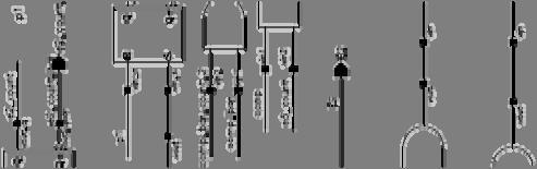
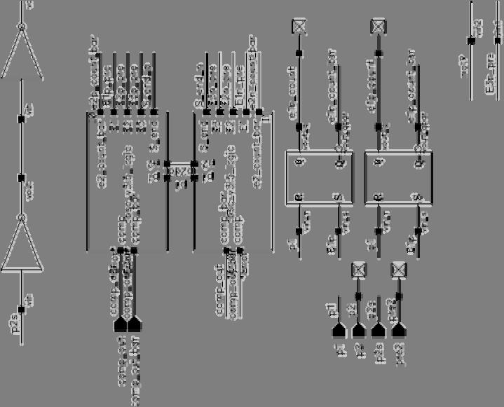
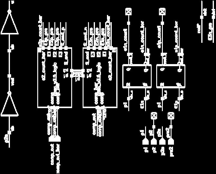
5 List of Figures Figure 2 1: Op-amp based switched-capacitor gain stage transfer phase. (a) Switched-capacitor circuit. (b) The output voltage exponentially settles to the final values. (c) The summing node voltage exponentially settles to the virtual ground condition.[4] Figure 2 2: Comparator-based switched-capacitor gain stage charge transfer phase. (a) Switched-capacitor circuit with an idealized zero delay comparator. (b) The output voltage ramps to the final value. (c) The summing node voltage ramps to the virtual ground condition. [4] Figure 2 3: Preset phase (P). (a) Switch P Closes. (b) grounded and brought below [4] Figure 2 4: Coarse charge transfer phase ( 1). (a) Current sourse 1 charges output. (b) and ramp and overshoot their ideal values.[4] Figure 2 5: Fine charge transfer phase ( 2). (a) Current source 2 discharges output. (b) and ramp to their final values. [4] Figure 2 6: CBSC pipelined ADC design [4] Figure 2 7: Sampling phase of pipelined ADC Figure 3 1: Noise shaping curves and noise spectrum in ΔΣ modulator Figure 3 2: Block diagram of a 2 nd -order feed-forward ΔΣ modulator
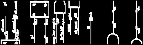
6 Figure 3 3: NTF and STF plot for 2 nd order ΔΣ modulator Figure 3 4: Op-amp based ΔΣ modulator block diagram Figure 3 5: Top level Schematics of an op-amp based 2 nd order ΔΣ modulator Figure 3 6: non-overlapping clock, phase-1 (P1) and phase-2 (P2) Figure 4 1: Single ended to differential conversion Figure 4 2: Pseudo differential design [7] Figure 4 3: Additional set of current course branch helps to make the CBSC operate without constrain on the input range Figure 4 4: Differential CBSC Block Diagram Figure 4 5: Current conflict between two CBSC driving stages Figure 4 6: CBSC ΔΣ modulator block diagram Figure 4 7: Latched comparator used in quantizer Figure 4 8: Sampling capacitor setups for quantizer Figure 4 9: Single ended version of intg1 with dummy branch Figure 4 10: Demonstration of transmission gate on-resistance Figure 4 11: a sample RC circuit with step input current Figure 4 12: a) Ideal behavior of comparator input voltage. b) Two types of effect caused by on-resistance of the switch. c) Resulting behavior after error correction Figure 4 13: State machine diagram for logic block Figure 4 14: Example of the use of SR-FF. a) Set up. b) Resulting signal Figure 4 15: comparator design for CBSC block Figure 4 16: Model of comparator offset voltage
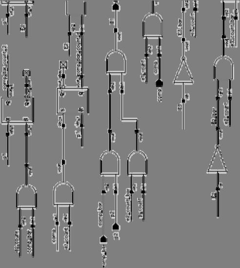
7 Figure 4 17: Error caused by comparator offset. A) Expected behavior. B) Error cases Figure 4 19: Comparator offset distribution Figure 4 19: Initial design of current mirror. A) E1 high, current source is on. B) E1 low, current source is off Figure 4 20: Comparison between the ideal current source and actual current source output currents Figure 4 21: basic structure of charge-pump style current source Figure 4 22: Equivalent circuit of charge-pump style current source when all the branches are off. is on the order of mega ohms Figure 4 23: Switch signals needs to match so that they reach about the same time Figure 4 24: Switches are sized in a way that Is2 = Is3 << Is1 to reduce the turn-off glitch at the output Figure 4 25: Simplified schematic of current source in CBSC block Figure 4 26: Top level schematics of a CBSC 2 nd order ΔΣ modulator Figure 5 1: Spectrum comparison of different versions of ΔΣ modulator
8 List of Tables Table 1 1: Comparison of the four types of ADCs... 8 Table 3 1: Coefficient values Table 4 1: capacitor sizing Table 4 2: Set-reset flip flop operation table [8] Table 5 1: Simulation setups Table 5 2: resulting SNR from different versions Table 5 3: Current usage comparison between the op-amp based and the CBSC based ΔΣ modulator
9 Chapter 1 Introduction 1.1 Motivation Advancement in modern technology has led to an increasing number of digital applications. However, because we live in an analog world, we need to convert the analog signals into digital signals before we can process them. The building block that is being used to accomplish this task is called an Analog-to-Digital Converter (ADC). There are a few major ways to build an ADC. Each of them has its pros and cons [1] [2] [3]. As can be seen in Table 1-1, ΔΣ ADCs have the advantage of offering the highest resolution of the various types. However, ΔΣ ADCs have several drawbacks as well. It has becoming more and more challenging to compensate op-amps for high gain-bandwidth in scaled technologies[4]. These ADCs also suffer an increase in power consumption (mainly from op-amp usage) in order to maintain conversion speed while the power supply is lowered [4]. In another words, op-amp has become the bottleneck of ΔΣ ADCs in terms of meeting the power consumption and speed requirements. As a potential solution to this problem, Comparator-based switched-capacitor (CBSC) circuits are introduced in [4] to eliminate the usage of op-amps. This thesis discusses the design and performance of a 2 nd order ΔΣ modulator using CBSC circuits. 7
10 Parallel design (i.e. flash ADC) Table 1 1: Comparison of the four types of ADCs Type Advantages Disadvantages Simple Fastest Can be non-linear DAC-based design (i.e. successive approximation) Pipeline ADCs Integrator-based design (i.e. singleslope) Delta-sigma (ΔΣ) design A single comparator can realize a high resolution ADC Buffered: last converted value can be read while the ADC is converting the current value Fast Low power High resolution Small die size Buffered Very high resolution Widely applicable *n = number of bits used in ADC Large number of components: 2 n -1 comparators Slow: requires 2 (n-1) clock cycles Latency Need calibration Needs a non-trivial analog Anti- Aliasing filter Calibration drift leads to inaccuracy over time Requires oversampling, which means higher than Nyquist rate clocks. Power consumption 1.2 Thesis Organization Chapter 2 provides a brief introduction to CBSC technology. The basic principles and operation of CBSC circuits are introduced in this chapter. Chapter 3 introduces an op-amp based feedforward 2 nd order ΔΣ modulator architecture. This architecture is the model of the CBSC 2 nd order ΔΣ modulator proposed in this thesis. Chapter 4 covers the design of a CBSC 2 nd order ΔΣ modulator. This chapter first discusses the architectural change to the op-amp based modulator. Then the details of each building block are presented along with changes made to the original CBSC technique. Chapter 5 shows the simulation results and comparison of the different versions of 2 nd order ΔΣ modulators: Matlab, op-amp based, CBSC based ideal component circuit, and CBSC based transistor level circuit. This chapter also provides a comparison of the power usage between an op-amp based ΔΣ modulator and a CBSC ΔΣ modulator. Chapter 6 8
11 discusses the advantages and the disadvantages of the CBSC ΔΣ modulator. In the end, future work and ideas are suggested in Chapter 7. 9
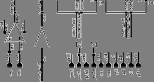
12 Chapter 2 Intro to CBSC 2.1 CBSC Circuits vs Op-Amp Based Circuits Fig. 2-1 and Fig. 2-2 from [4] both use the switched-capacitor architecture; however, in Fig. 2-2 the op-amp in Fig. 2-1 is replaced by a comparator. The main difference between the two building blocks is that the op-amp forces the virtual ground while the comparator detects the virtual ground. The output voltage plots show that they both have similar behavior, except that one settles exponentially while the other one settles linearly. It can also be mathematically proven that the comparator-based circuit works the same as the op-amp based circuit (see Appendix A.1 and A.2). There are several advantages of the comparator-based switched-capacitor (CBSC) topology. First, just like the op-amp based switched capacitor circuits, the CBSC circuits use two-phase clocking, sampling phase and evaluation phase. The difference is that in a CBSC circuit all the current sources connected to the output nodes are off at the end of the evaluation phase, which is good for low-voltage applications [5]. Second, preliminary analyses indicate that detecting the virtual ground condition (CBSC circuits) is more energy efficient than forcing the virtual ground (op-amp based circuits)[6]. Also, the op-amp approach has a feedback path, which 10
13 Figure 2 1: Op-amp based switched-capacitor gain stage transfer phase. (a) Switched-capacitor circuit. (b) The output voltage exponentially settles to the final values. (c) The summing node voltage exponentially settles to the virtual ground condition.[4] Figure 2 2: Comparator-based switched-capacitor gain stage charge transfer phase. (a) Switched-capacitor circuit with an idealized zero delay comparator. (b) The output voltage ramps to the final value. (c) The summing node voltage ramps to the virtual ground condition. [4] 11
14 needs to be stabilized. The techniques used to stabilize the amplifier require increased power consumption to maintain the same operational speed [4]. On the other hand, CBSC does not have a stability problem because it has an open-loop. Thus, CBSC doesn t consume as much power. Finally, the CBSC design methodology is expected to be applicable to a wide range of capacitively loaded switched-capacitor circuits and expected to be compatible with most known architectures [4]. However, successful implementation of CBSC ΔΣ modulator with real test results is not demonstrated in literature yet. 2.2 CBSC Charge Transfer Phase Even though a CBSC circuit behaves very similarly to an op-amp based circuit, it has a very unique charge transfer phase. Fig. 2-3, Fig. 2-4, and Fig. 2-5 from [4] shows the three charge transfer steps: preset phase (P), coarse charge transfer phase (E1), and fine charge transfer phase (E2). During the preset phase (Fig. 2-3), node is grounded, brought below (see Appendix A.2 for calculation). During coarse charge transfer phase in Fig. 2-4, current source E1 provides current to the rest of the circuit until equals to. As a result, it successfully integrates the current value (see Appendix A.2). However, the charge transfer process is not so perfect in reality, because non-ideality exists in the circuit. One source of error comes from the comparator delay, which causes to overshoot, as shown in Fig. 2-4, b). 12
15 Figure 2 3: Preset phase (P). (a) Switch P Closes. (b) grounded and brought below [4] Figure 2 4: Coarse charge transfer phase ( ). (a) Current sourse charges output. (b) and ramp and overshoot their ideal values.[4] 13
16 To overcome the overshoot caused by comparator delay, another current source E2 is added to correct this error. Instead of providing current, current source E2 sinks current causing current to reverse until the voltage drops below. Because the current of E2 is much smaller than current of E1, the overshot will be much smaller than the original one. Thus, E2 acts as an overshoot correction phase, Fig Figure 2 5: Fine charge transfer phase ( ). (a) Current source discharges output. (b) and ramp to their final values. [4] 2.3 CBSC Application in Pipelined ADC A common application of the CBSC circuit is in pipelined ADC design [4], Fig Here, the CBSC circuit is used to provide a constant gain of, using the direct charge transfer (DCT) sampling method, Fig
17 Figure 2 6: CBSC pipelined ADC design [4] Figure 2 7: Sampling phase of pipelined ADC 15
18 To guarantee that always drop below, the input is limited to a certain range [9] After preset (2.1) 2 (2.2) In the case of 0 (2.3) then (2.4) This limits the input range to at most only half full scale. This limitation causes problem for ΔΣ modulator, which is discussed in chapter 4. 16
19 Chapter 3 An Op-Amp Based Ideal Circuit Design The basic theory of the comparator-based switched-circuit (CBSC) is explained in Chapter 2. The next step is to apply this theory to a practical design of a 2 nd -order ΔΣ modulator. This chapter provides a brief overview of a particular op-amp based ΔΣ modulator structure that is being converted to a CBSC version. 3.1 Operation and Architecture ΔΣ modulation is based on the technique of oversampling to reduce the noise in the band of interest (left shaded area of Fig. 3-1 [7]), which also avoids using high-precision analog circuits for the anti-aliasing filter [7]. Another important property of ΔΣ modulator is noise shaping. For a first order ΔΣ modulator, noise is being shaped by the function 1 ; for a n th order ΔΣ modulator, noise is being shaped by the function 1, resulting in in-band quantization noise variance to equal to [7], where OSR represents the oversampling rate. On the system level, there are many ways to realize a ΔΣ modulator. Richard Schreier has provided a very convenient MATLAB tool box delsig (available at 17
.")

20 to calculate the coefficients for various orders and types (feed-forward, feed-back etc.). Figure 3 1: Noise shaping curves and noise spectrum in ΔΣ modulator For this project, a commonly used 2 nd -order feed forward ΔΣ modulator is chosen, with system level block diagram shown in Fig Each block can be modeled as a delay unit with feedback, which represents an integrator: 1 1. The coefficients, listed in Table 3-1, are chosen to make sure that the voltage swing at each stage is well within range of Vdd (2V) and Vss (ground). The overall DC gain of the modulator is (see Appendix A.4 for mathematical calculation). The signal transfer function (STF) and noise transfer function (NTF) of this modulator are shown in Fig
21 Figure 3 2: Block diagram of a 2 nd -order feed-forward ΔΣ modulator Table 3 1: Coefficient values Coefficient Value

 with a non-delayed feed-forward path. The third block is a quantizer (qtzr) with gain of 3.")
22 Figure 3 3: NTF and STF plot for 2 nd order ΔΣ modulator 3.2 Circuit Implementation The top level block diagram of the op-amp based ΔΣ modulator is shown in Fig. 3-4, and the top level schematic is shown in Fig The first block is a delayed integrator (intg1) with a simple built-in digital-to-analog convertor (DAC) to convert the digital output of the quantizer to certain voltage. The second block is a delayed integrator (intg2) with a non-delayed feed-forward path. The third block is a quantizer (qtzr) with gain of 3. Vin intg1 intg2 qtzr z z z z -1 Gain = 3 Vout DAC Figure 3 4: Op-amp based ΔΣ modulator block diagram 20
23 Figure 3 5: Top level Schematics of an op-amp based 2 nd order ΔΣ modulator 21
24 In the op-amp based design, analog data is being converted to digital data after two and a half cycles. Each cycle has two non-overlapping clocks, phase-1 and phase-2, as in Fig For the first cycle, intg1 samples from the input and the output from DAC during phase-1, and integrates during phase-2. The output of intg1 becomes available by the end of phase-2. For the second cycle, the delayed integration path samples previous cycle s intg1 output data during phase-1, and integrates the data during phase-2. On the other hand, the non-delayed feed-forward path directly passes the intg1 output data of the current cycle during phase-2 to the output. The outputs of both paths become available by the end of phase-2 of the second cycle. In the mean time, qtzr samples the outputs of intg2 during phase-2 of the second cycle, and outputs logic signal during phase-1 of the next cycle, which is being fed back to the DAC of intg1. The modulator then keeps repeating the above process. Figure 3 6: non-overlapping clock, phase-1 (P1) and phase-2 (P2) As mentioned in chapter 1, op-amps are not very power efficient for modern switchedcapacitor circuit design. Chapter 4 describes a comparator-based attempt to build this 2 nd order ΔΣ modulator with lower power. 22
25 Chapter 4 CBSC 2 nd Order Modulator Mathematically, the CBSC block works pretty much the same as an op-amp; however, there are many differences when it comes to circuit design. This chapter describes some changes made to the basic 2 nd order ΔΣ Modulator structure, and the implementation of a CBSC version. 4.1 Differential CBSC without Preset Phase In order to get better performance, a differential version is designed based on the original single-ended CBSC circuit. It is very easy to get a pseudo differential version. Imagine that there are two inputs at the input of two identical single-ended CBSC integrators: the input at is initially larger than input common mode voltage ( ), and the input at is smaller than. The resulting and voltages are shown in Fig. 4-1 a). Put the two single-ended CBSC blocks together, Fig. 4-1 b), we get a pseudo differential version, Fig. 4-2 [10]. 23
 b) Figure 4 1: Single")

26 E1 E2 i) Vxp E1 E2 Vcm Vxp ii) Vcm Vxn Vcm Vxn a) b) Figure 4 1: Single ended to differential conversion Figure 4 2: Pseudo differential design [7] 24
27 However, this design has a few problems. The positive branch and the negative branch are completely independent of each other. Any mismatch or delay will cause the two branches to act differently and as a result the input and output common mode voltage will be shifted. Also, the normal output common mode voltage regulation circuits cannot be used for CBSC circuits [4]. Drifting common mode voltages will eventually drive the outputs towards one of the rails and disable the modulator. Additionally, preset phase does not work very well for this differential modulator. Recall that the whole purpose of preset phase in the original CBSC design is to pull below, Fig In the pipelined ADC design in section 2-3, the CBSC block is used to provide a constant gain. During the sampling phase, the feedback capacitor is reset each period. In this pipelined ADC case, the condition is easier to predict: drops below as long as the input is within. However, in a ΔΣ modulator, the situation is more complicated. The CBSC block is used in an integrator. Its feedback capacitor never gets reset. In this case, is affected by both the input and the output voltages. For an integrator, in order to make sure drops below after preset, the following equations need to be satisfied (see Appendix A-2 for detailed calculations): 2 0 (4.1) (4.2) (4.3) (4.4) The condition in equation 4.4 is not always true in a ΔΣ modulator, and the modulator will fail to operate. A more robust design is needed for ΔΣ modulator. Because the preset phase can no 25
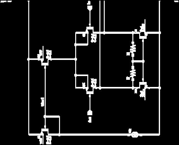
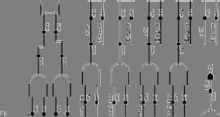
28 longer do the job it supposed to, it is taken out of the design. Instead, a second set of current sources are added so that it works regardless of the input combinations, as seen in Fig If, then the set is being used to source current; if, then the set is being used to sink current. See section 4-7 for details about the current source. Calculations in Appendix A.3 show that there is no theoretical difference between the revised CBSC block without preset phase and the original CBSC block with preset phase. Figure 4 3: Additional set of current course branch helps to make the CBSC operate without constrain on the input range Figure 4 4: Differential CBSC Block Diagram 26
29 4.2 CBSC Feed-Forward Path Issue Even though the CBSC circuits behave similarly as the op-amp circuits do, but there is a fundamental difference: CBSC circuits cannot support a feed-forward path, which is commonly used in op-amp circuits. To illustrate this difference, Fig. 4-5 shows a feed-forward path between intg1 and intg2, with CBSC block replacing op-amp. Originally, this feed-forward path works fine with op-amps, because op-amps can provide current at all time. Also, op-amp based integrators do not care how the currents are moving as long as they eventually settle. However, CBSC blocks are very sensitive to the movements of currents and the change of voltage at its input. As it shows in Fig. 4-5 a), the feed-forward path between intg1 and intg2 causes conflict between current and at the capacitors between them. Also, depending on the input at each integrator, intg1 and intg2 may finish integrating at different times. Once the integration of intg1 finishes, current sources of the CBSC block in intg1 is shut off, disconnecting the load capacitors, which are also the input sampling capacitors of intg2, Fig. 4-5 b). The charge is no longer available for the feed-forward path. On the other hand, op-amp based integrator can function with the feed-forward path in intg2, because the opamp can provide output current at any time as long as the input is not disturbed. In conclusion, the CBSC based intg2 cannot be used as a summer like the one in an opamp based intg2. To solve this problem, the feed-forward path is separated from intg2, so that there is no summation in intg2. Instead, qtzr samples results from intg1directly during phase-2, and combines that result with intg2 output. Fig. 4-6 is the updated system block diagram. It is desired to compare the sum of the differential outputs of the two integrators, 27
30 , with the three reference levels of the quantizer: ( ), 0, and ( ). Figure 4 5: Current conflict between two CBSC driving stages Three latched comparators are used in the quantizer, Figure 4-7. Their outputs follow the following equation: (4.5) 28
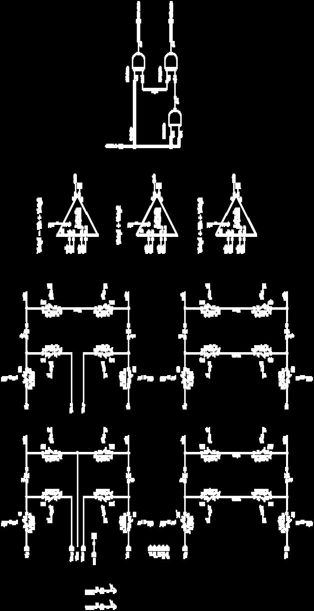
31 If Q is positive, the comparator outputs logic high; if Q is negative, the comparator outputs logic low. For example, in order to compare with ( ), the quantizer needs to sample the outputs in a way that:. (4.6) Fig. 4-8 a) and c) demonstrates the circuit implementation. It is easy to confirm that (4.7) (4.8) (4.9) (4.10) The desired comparison is obtained by connecting to pin of the latched comparator, and,, to,, pins respectively. The other two comparisons can be arranged in the similar manner. Figure 4 6: CBSC ΔΣ modulator block diagram 29

32 Figure 4 7: Latched comparator used in quantizer Figure 4 8: Sampling capacitor setups for quantizer 30
33 4.3 Delay The second problem is that the output of CBSC integrator is only available during the integration phase, phase-2. During the sampling phase, phase-1, the loading capacitor is floating, and the CBSC block is unable to provide any charge for the next stage to sample. It means that intg2 cannot sample the intg1 outputs during phase-1, as it does in the op-amp based modulator. To solve this problem, dummy branches are added to intg1 to realize a half cycle delay,. Fig. 4-9 shows a simplified single ended version of intg1 with added dummy branch. This dummy branch samples zero as its input during phase-2, and integrates zero during phase-1. This operation would not change the previous result of, but it provides current for the next stage to sample during phase-1. However, because integration happens twice, the overshoot error is created both times. Effectively, the overshoot error doubles, which is a drawback of this structure. It also draws more power because of the additional integration. Figure 4 9: Single ended version of intg1 with dummy branch 31
34 4.4 Capacitor Sizing There are a few factors that affect the sizing of the sampling capacitors in this modulator. One dominant factor is the thermal noise associated with the capacitors of the first stage, intg1. The thermal noise power can be estimated by 1 (see Appendix A.6 for the mathematical calculation), where 2 for modulator coefficients, 3 to match the input capacitors, and OSR equals to 250 in this CBSC ΔΣ modulator. To ensure that the thermal noise wouldn t be a dominate noise source, the signal to thermal noise ratio should be at least 6 db lower than signal to quantization noise ratio: 10 log, 6. To be safe, S is set equal to 86 db. SNR here is set to smaller than SNR of a traditional op-amp based modulator due to the limitation of a CBSC based modulator. Then plug in values and solve, is found to be bigger than 1.2pF. The capacitors in 2 do not contribute as much input referred thermal noise, which means that the capacitors in Table 4 1: capacitor sizing Capacitor Description Value input sampling capacitor for intg1 1.8 pf 2 DAC sampling capacitor for intg1 1.2 pf 6 feedback capacitor for intg1 5.4 pf 2 input sampling capacitor for intg pf 2 feedback capacitor for intg2 2.7 pf 2 input sampling capacitor for qtzr 1 pf 8 32
35 intg2 could be even smaller. However, because leakage currents have greater effect on smaller capacitors than larger ones, the capacitors cannot be too small. Also, larger capacitors require larger current. As a result, the capacitor sizes are set as shown in Table 4-1 for a better overall performance of the modulator. The optimal values yet need to be found. 4.5 Sampling Switches The switches of the sampling branches are mostly transmission gate, with characteristics shown in Fig The relative sizes of the p-mos and n-mos of the transmission gate control the onresistance of the switch. In general, it is desired to make the peak of the on-resistance happen at the middle of the possible voltage range between and. Figure 4 10: Demonstration of transmission gate on-resistance There is one undesired effect of the switch on-resistance. Fig shows a simplified circuit to demonstrate this effect. The current source of the CBSC block is modeled as a simple current source with a step input. Once the current is turned on, a constant current goes through the resistor and charges the capacitor, which makes the voltage across the capacitor ramps up 33
36 linearly. The current also causes a voltage drop across the resistor, makes steps up instantly, where. This glitch can be ignored at any node of the circuit expect, input node of the CBSC block. As it mentioned in previous section, the positive branch and negative branch are mirrors of each other. and travels in different direction, which means the glitch will cause the voltages at these two nodes either become farther apart (error1) or closer (error2) at the moment when the current sources are turned on or off, see Fig b). Error1 causes longer integration time. If the CBSC block takes too long then it may not be able to finish integrating before the end of the integration phase, very big overshoot error will result. Error1 is not recoverable and is not acceptable for for ΔΣ modulator. Also, this glitch can cause false triggering, error2. This error causes the logic of CBSC circuit to stop providing current too early that E2 doesn t even start. Error2 causes larger overshoot error than expected. Figure 4 11: a sample RC circuit with step input current. 34
37 E1 E2 i) Vxp E1 E2 error1 i) Vxp E1 E2 error1 Vxp Vxn Vxn Vxn End of integration phase ii) Vxp E1 error2 ii) Vxp E1 E3 error2 Vxn a) b) t1 Vxn c) Figure 4 12: a) Ideal behavior of comparator input voltage. b) Two types of effect caused by on-resistance of the switch. c) Resulting behavior after error correction. The error from on-resistance of the switch is inherent in the circuit and cannot be avoided. To make sure the CBSC circuit finish integrating in error1 situation, a larger current during is being used. This bigger current will cause bigger overshoot than original, but it makes sure the integrator finishes integrating. As for error2, it is pretty easy to detect the happening of error2, because the glitch usually takes much shorter time than. We can check the status of the current source at time in Fig b): if is on, then error2 will not happen; if is not on, then error2 happens. Logic block is updated from the ideal version so that it can detect error2 and turn on the corresponding current,, to pull and closer, see Fig c). 35
38 4.6 CBSC Logic Block The CBSC logic block is the brain of the ΔΣ modulator. It takes a comparator result as input, and outputs a signal to turn on or off the current sources. The logic for this proposed CBSC ΔΣ modulator is represented in a state machine diagram in Fig In each state, the corresponding signal (named the same way as the state) goes high and the rest go low. When the CBSC block is in Idle, no current is provided. The integration phase clock acts as the start signal: depending on the comparator output, the state either goes to E1p (the top half path) or E1n (the bottom half path). Once the comparator output flips, the state goes to E2 trying to correct the overshoot. Next, depending on whether the glitch (error2) in Fig b) happens, the state either goes back to Idle, or goes to E3 to try to correct the overshoot again. Figure 4 13: State machine diagram for logic block 36
39 As shown in the state machine diagram, it's the change of the comparator output values ( or ) that triggers the change of states. In order to know which state is next, logic block needs to know what the current state is. For this purpose, set-reset flip flops (SR-FF) are used as counters. The operation of the SR-FF are summarized in Table 4-2 [8]. The reset (R) signal is the sampling clock for each SR-FF, so that the states are reset in idle state. The set (S) signal is the corresponding signal in each state. Once that signal goes high, the SR-FF is set and will not be reset till the next phase. For example, in order to create _ and _ signals to indicate that or have come up, the SR-FFs are connected as shown in Fig a), the outputs are shown in Fig b). E _ and E _ are low in the beginning. During, remains low the whole time. Once E goes high, SR-FF set _ to high. After drops low, E goes high, SR-FF set _ to high. Then, _ and _ remains high until goes high to reset them. These output signals created by the SR-FF are good indications of whether certain state has occurred or not. Table 4 2: Set-reset flip flop operation table [8] SR Flip-Flop operation Characteristic table Excitation table S R Action Q(t) Q(t+1) S R Action 0 0 Keep state X No change 0 1 Q = Set 1 0 Q = Reset 1 1 Unstable combination, race condition 1 1 X 0 No change ('X' denotes a do not care condition; meaning the signal is irrelevant) 37
40 Figure 4 14: Example of the use of SR-FF. a) Set up. b) Resulting signal. Notice that the conditions for state going from Idle to E1n and from E1p to E2n are pretty much the same. In order to prevent the state to go from E1p to E1n and E2n at the same time, the signal indicating that E1p has occurred is used to determine if E1n should be the next state or not. The signals are created by common digital gates, such as and-gate, or-gate, and inverter, etc. They are all standard units. Because their real transistor level model behaves very similar to their Verilog behavioral models, Verilog behavioral models are used for convenience. The rise and fall time of the digital gates are set to 100ps. 38
41 4.7 Comparator The comparator is one of the most important parts, because the comparator delay and decision error directly affects the performance of a CBSC block. Just the comparator alone can be expanded to a full PHD thesis. Due to the scope and purpose of this project, a simple 3-gainstage comparator design is used. As shown in Fig. 4-15, the comparator consists of three stages: differential amplification stage, differential to single ended amplification stage, and finally a common-source output stage. All three stages provide gain to make sure the comparator outputs full logic level even with very small differential input. One drawback of having multiple stages is that it is relatively slow, because there is cumulated delay from each stage. Each comparator draws about ~40 current. Figure 4 15: comparator design for CBSC block In an op-amp based ΔΣ modulator, op-amp offset voltage does not cause error; however, in a CBSC based design, directly causes error in CBSC block. For op-am based ΔΣ modulator, this non-signal-dependent can be modeled as a constant input in the loop, Fig. 39
42 4-16. This constant input is suppressed by the modulator s loop gain and does not reduce modulator accuracy much at all. This conclusion is also verified by Matlab simulation. The simulation without manually added gets 114 db SNR, while the simulation with manually added gets 112 db SNR. The performance is almost the same. On the other hand, for a CBSC based design, the bigger the offset the bigger the integration error. Fig a) shows the expected behavior of the CBSC block without. With comparator offset, instead of comparing to, compares to +/- and gives decisions at the wrong time. Fig.4-17 b) shows the resulting effects (exaggerated) caused by. and are not brought together as close as expected and causes bigger error. Figure 4 16: Model of comparator offset voltage 40
43 Vxp i) Vxp Vxn Vxn-Voffset Vcomp Vxp Vxn Vcomp_with_delay Vcomp Vcomp_with_delay ii) Vxp Vxn+Voffset Vxn Vcomp Vcomp_with_delay a) b) Figure 4 17: Error caused by comparator offset. A) Expected behavior. B) Error cases The input referred offset voltage ( ) of the comparator used in this project is about 2mV without mismatch. However, component mismatch is unavoidable in real process. Fig shows the statistic distribution of when there is mismatch. Even though is centered around 1mV, it has a very wide variation. Optimization for comparator and delay is definitely needed for a high precision CBSC ΔΣ Modulator. 41
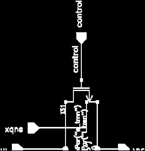
44 4.8 Current Source Figure 4 18: Comparator offset distribution The current sources either source current to or sink current from the rest of the circuit in order to bring the two input nodes of the comparator ( and ) closer. The initial design is to use cascode current mirror with switches to turn each branches on or off. Fig demonstrates how to turn a branch on and off. When signal is high _ is 42
45 low, the output branch is properly biased and provides current. When is low and _ is high, the corresponding switch closes and pulls the gate voltage of to. As a result, the current of the output branch is turned off. Figure 4 19: Initial design of current mirror. A) E1 high, current source is on. B) E1 low, current source is off. There are a few issues with this design. The desired gate voltage of is around 1.2V when current source is turned on, and (2V) when current source is turned off. In another words, at the moment of current source turned on or off, the gate voltage swings between 1.2V and 2V, this is a pretty big swing. As a result, it requires a lot of charge to charge or discharge the parasitic capacitances at the gate of, It takes quite some time to settle to the desired value. The sudden change of bias voltage also creates large overshoot as shown in Fig As it is mentioned in chapter 2, the CBSC overshot error is proportional to comparator delay and current source value. Therefore, if the output current cannot settle to the expected value before it turns off, an undesired large CBSC overshot error will be created as a result. 43
46 Figure 4 20: Comparison between the ideal current source and actual current source output currents An alternative design used in the final version is a charge-pump style current source. The basic idea is presented in Fig The bias current is made by a simple current mirror instead of a cascode current mirror, because maximum output swing is desired. The bias current is on at all time, and the current is being steered to the desired output based on the switch signals. At the end of integration of the CBSC integrator, instead of being shut down completely, the current directly goes to ground (or of the circuit) through an internal path, so that effectively there is no current circulation in the external circuit. Figure 4 21: basic structure of charge-pump style current source 44
47 This charge-pump style current source can reach its desired value much faster than the switched current mirror version. Because the charge-pump style current source doesn t change any bias voltage of the bias current during transition, it avoids the large overshoot and long settling time. One thing to be aware of is that at least one of the switches in the charge-pump style current source has to be on at any given time, in order to provide a complete path for the current. The switches are transmission gates with very large off-resistance (on the order of mega ohms). If all the switches are off, Fig. 4-22, the bias current goes through the large off-resistance, voltage at node-1 will instantly raise to. At that instant, the branch will be effectively shut off and will act the same as the previous described current mirror, which is not good. Therefore, the switch signals need to match each other in a way that they always meet each other at the midpoint voltage ( 1 ) at about the same time, as shown in Fig At that moment, all the paths are partially on with the on-resistance of the transmission gate at approximate the maximum value. Figure 4 22: Equivalent circuit of charge-pump style current source when all the branches are off. is on the order of mega ohms 45
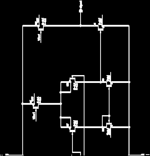
48 Figure 4 23: Switch signals needs to match so that they reach about the same time To avoid the turn-off glitch of the output branches, the S1 switch is made larger, meaning it has smaller on-resistance than the switches of the output branches. In this way, even if all the paths are all partially on, most of the current will go through the internal path, so that the output is not affected, Fig On another note, the on-resistance of the output branch switches cannot be made too big, otherwise it will cause large voltage drop across the switches and limits the output swing of the CBSC block. Figure 4 24: Switches are sized in a way that Is2 = Is3 << Is1 to reduce the turnoff glitch at the output A simplified schematic of the final design of the current source for the CBSC block is shown in Fig See Appendix B.1.6 for full schematic diagram. The current source block 46
49 receives four logic signals as input,,,,, and outputs corresponding currents to the positive branch ( ) or the negative branch ( ). As stated earlier, when the outputs do not need any current, the currents are directed to or (ground) internally and wasted. Notice that and are mirrors of each other. When needs, needs ; when needs, needs, and vice versa. In another words, path can just use the unused branch from path. Then, each branch of the current source is shared between and to save current. Also, and will not be on at the same time. In order to not waste when is not on, and are combined together to deliver current during. Figure 4 25: Simplified schematic of current source in CBSC block The branches of the current source block are sized in a way that roughly. How does one decide what value should and be? Mathematically, constant current charges capacitor in the manner described in the following equations, where is the differential input for that cycle, and is the overshoot voltage of a single end after E1 state. 47
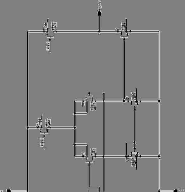
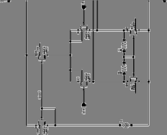
50 2 (4.11) 2 (4.12) The goal is to find a current pair ( and ), so that integration time of each cycle. A minimal is desired, because the size of direct affects the final overshoot voltage: the smaller the smaller overshoot, and the better accuracy as a result. Ideally should be almost constant for a particular comparator and a particular value. Using the largest possible differential input for safely, one can find an estimated current pair using the above equations. It s only an estimate because there are a lot of non-idealities in real circuit design, such as comparator delay is signal dependent and does not stay constant, etc. Minor tweaks are necessary for optimal performance. 4.9 Prototype CBSC 2 nd Order Modulator With the updated 2 nd order modulator architecture, CBSC integrators, and qtzr from the original op-amp design, a prototype CBSC 2 nd order modulator is implemented using TSMC.18 technology. The digital gates used in the logic blocks are behavior model, so that the parameters are easy to change for the simulation. The top level schematic is demonstrated in Fig Please refer to chapter 5 for simulation results and comparison against the op-amp based modulator. 48
51 Figure 4 26: Top level schematics of a CBSC 2 nd order ΔΣ modulator 49
52 Chapter 5 Simulation Result 5.1 SNR Cadence is used to simulate different versions of the modulator. The setup is in Table 5-1. Matlab then is used to process the sum of qtzr output data and create spectrums for comparison, Fig The resulting SNR for each version is listed in Table 5-2. The CBSC based ideal circuit version has a 30 db drop from the mathematically calculated noise-free result, while the op-amp based ideal circuit version can perform almost perfectly. The reason for the performance difference is that for the ideal circuit, the op-amp gain can be set very large and achieve almost no error. However, the logic for CBSC version is generated using several stages of digital gates. Even though digital gates are generally very fast, long enough delay is accumulated after several stages. As a result, overshoot error is unavoidable, which decreases the accuracy. The accuracy of the CBSC ΔΣ modulator is further decreased from the ideal version to the transistor level design. The main error comes from the comparator overshoot error and delay. The glitch caused by the on-resistance of the switch is also a factor. More careful design is necessary to push the performance of this transistor level design. 50
53 Table 5 1: Simulation setups Input frequency 4 khz Sampling frequency 10 MHz T Sampling period 100 ns Clock and width 47.3 ns Differential input voltage amplitude 1 rmsv Top rail power supply voltage 2 V Common mode voltage 1 V Ground 0 V Raise time of the digital gates and clocks 100 ps Fall time of the digital gates and clocks 100 ps _ The coarse charge current of integrater _ The fine charge current of integrater _ The coarse charge current of integrater _ The fine charge current of integrater OSR Over sampling ratio
 114.20 Op-amp based Ideal version 112.89 Op-amp based real transistor version ~ 90 CBSC based ideal version 81.14 CBSC real transistor version 60.")
54 Figure 5 1: Spectrum comparison of different versions of ΔΣ modulator Table 5 2: resulting SNR from different versions Version SNR (db) Matlab (without noise) Op-amp based Ideal version Op-amp based real transistor version ~ 90 CBSC based ideal version CBSC real transistor version
55 5.2 Power Usage Despite the lower accuracy, the CBSC ΔΣ modulator shows a big advantage in power saving over the op-amp based design. Table 5-2 is a comparison of the power usage and performance of the two designs. The power usage of qtzr is not listed, because qtzr from the original op-amp version is used for the CBSC modulator. If we use ENOB over power usage as a figure of merit to compare the two versions, CBSC modulator shows its advantage. In this project, the CBSC modulator is a trial version. There is lots of room for improvements. The performance should be able to be pushed closer to ideal and achieve close to 80 db SNR. Table 5 3: Current usage comparison Op-amp based CBSC based Intg1 700 Current source Comparator Current Usage Intg2 150 Current source Comparator Total ENOB 16 bit 9.7 bit FOM = ENOB/Power 9.41 bit/nw bit/nw 53
56 Chapter 6 Conclusion A new comparator-based switched-capacitor 2 nd order ΔΣ modulator is presented. This CBSC modulator has a number of advantages compared to the original op-amp based design. As demonstrated in chapter 5, the CBSC modulator consumes much less power, but has yet to match the performance of the op-amp based design. It is appropriate in applications that have very tight power requirement but not very strict accuracy. One may argue that power and accuracy are always a trade-off: if targeting lower accuracy, an op-amp can use less power also. However, there is a limit. When the current is lower than a certain limit, op-amps will not settle at all. For example, the original modulator would not be able to operate at the power level of this CBSC modulator. Also, CBSC methodology is more amenable to design in scaled technology. Instead of forcing the virtual ground, CBSC design detects the equal condition in an open-loop manner, so it does not have stability issues as op-amps. Finally, CBSC is compatible with most known architectures, with minor change. One issue of CBSC design is discussed in section 4.2: CBSC designs can only drive switched-capacitor loads. CBSC design cannot drive another stage directly. For those designs that have a direct driving stage, architectural adoption is needed. 54
57 Chapter 7 Future Work and Ideas Some suggestion and ideas for future work: An optimized design (shorter delay and low offset voltage) of the comparator in CBSC will help increase the accuracy. Overshoot cancellation technique in [4] may shorten the integration time or increase accuracy, because a smaller fine charge current can be used. To further save power, the current source and comparator can be turned off while they are not being used (in idle state). However, in order to avoid possible harmful turn-on transient behaviors, an advanced clock may need to be used to turn them on a little bit before their outputs are supposed to be used. The smaller the capacitors used in the integrators the smaller the charging currents. To further save power, one may use smaller capacitors. But be careful with the leakage currents. Noise, non-ideality, and non-linearity analysis 55
58 Appendix A Calculations This appendix provides some mathematical proofs to the functionalities of CBSC circuits discussed in this paper. The comparison between the CBSC circuits and the traditional op-amp based circuits are demonstrated also. A.1 Op-Amp Based Integrator Mathematical derivation of the z-transform of an op-amp based integrator is demonstrated in this section. Clock: Here P 1 is the sampling phase, and P 2 is the integration phase. Ideal Op-Amp: 0 virtual ground. 56
59 At : At : At : 2 Combine the above results: Z-transform:

60 A.2 CBSC Integrator with preset phase Mathematical derivation of the z-transform of a CBSC based integrator with preset phase is demonstrated in this section. This is the original configuration introduced in [4]. 1) During : 2) During preset (P) in : 0 (demonstrated as grounded, but it should be connected to the lowest voltage possible) Charge Balance: 58
61 2 3) During charge transfer (E) in : 2 0 Same amount of charge goes through : 2 Also From the above we get 59
62 1 Same form as the op-amp based integrator. 60
63 A.3 Proposed CBSC Integrator without Preset Phase Mathematical derivation of the z-transform of a CBSC based integrator without preset phase is demonstrated in this section. This is the configuration designed base on the original one in [4], and is proposed for the CBSC 2 nd order ΔΣ modulator discussed in this paper. During P1: During P2: 1) 61
64 2) 2 Combine the above: Same result with the one with preset 1 62
65 A.4 DC Gain of the 2 nd Order Modulator Below is the block diagram of the 2 nd order ΔΣ modulator built in this paper. This section provides the mathematical calculation of its overall DC gain. Coefficients are: =1; = ; = ; =, with build in gain of 3 in qtzr. Use Mason s rule to find the gain without : The forward paths and gains ( : The loops and their gains: Δ : 1 the loops remaining after removing path j. If none remain, then Δ = 1. Δ 1 and Δ 1 63
66 Δ: 1 - Σ loop gains + Σ non-touching loop gains taken two at a time - Σ nontouching loop gains taken three at a time + S non-touching loop gains taken four at a time total gain Δ Δ Δ For DC gain 1: Overall gain: b M
67 A.5 Comparator Offset Model CBSC Comparator Offset Same results as A.2 before phase E. During E in phase 2, the current source is shut off when instead of. 1) 2) 3) 0 Rearrange modeled as: The above equation shows that in the ΔΣ loop, the comparator offset voltage can be 65
68 A.6 Calculation of modulator thermal noise This section provides a mathematical calculation of the thermal noise of a differential integrator used in the CBSC 2 nd order ΔΣ modulator. Dummy Branch P2 Cdummy P1 CFB P1 P2 Input Branch Vin P1 Cin P2 P2 P1 DAC Input Branch Vref P1 CDAC P2 P2 P1 CBSC Vout The above figure demonstrates a single ended intg1 with three branches: (1) input, (2) DAC, (3) and dummy branch. The input referred thermal noise (KT/C noise) can be calculated as follows. For (1) For (2) For (3) 66
69 Total thermal noise for single ended modulator (one phase ) _ 1 Total thermal noise for fully differential modulator (both phases) 1 _


70 Appendix B Schematics This appendix shows the schematics of the 2 nd order ΔΣ modulator designed in this paper. B.1 Top Level 68


71 B.2 Intg2 (sampling stage is included in intg1) 69


72 B.3 CBSC without Dummy Branch 70


73 B.4 Logic of CBSC without Dummy Branch 71
74 B.5 Comparator in CBSC 72


75 B.6 Current Source in CBSC 73


76 B.7 Intg1 (Including sampling stage of intg2) 74

77 B.8 UnitDAC 75


78 B.9 CBSC with Dummy Branch 76


79 B.10 Logic of CBSC with Dummy Branch 77

80 B.11 Qtzr in CBSC 78


81 B.12 Transmission Gate 79


82 B.13 Reference Voltages in CBSC 80
Analog CMOS Interface Circuits for UMSI Chip of Environmental Monitoring Microsystem
 Analog CMOS Interface Circuits for UMSI Chip of Environmental Monitoring Microsystem A report Submitted to Canopus Systems Inc. Zuhail Sainudeen and Navid Yazdi Arizona State University July 2001 1. Overview
Sigma-Delta ADC Tutorial and Latest Development in 90 nm CMOS for SoC
 Sigma-Delta ADC Tutorial and Latest Development in 90 nm CMOS for SoC Jinseok Koh Wireless Analog Technology Center Texas Instruments Inc. Dallas, TX Outline Fundamentals for ADCs Over-sampling and Noise
CMOS High Speed A/D Converter Architectures
 CHAPTER 3 CMOS High Speed A/D Converter Architectures 3.1 Introduction In the previous chapter, basic key functions are examined with special emphasis on the power dissipation associated with its implementation.
A PSEUDO-CLASS-AB TELESCOPIC-CASCODE OPERATIONAL AMPLIFIER
 A PSEUDO-CLASS-AB TELESCOPIC-CASCODE OPERATIONAL AMPLIFIER M. Taherzadeh-Sani, R. Lotfi, and O. Shoaei ABSTRACT A novel class-ab architecture for single-stage operational amplifiers is presented. The structure
Design And Simulation Of First Order Sigma Delta ADC In 0.13um CMOS Technology Jaydip H. Chaudhari PG Student L. C. Institute of Technology, Bhandu
 Design And Simulation Of First Order Sigma Delta ADC In 0.13um CMOS Technology Jaydip H. Chaudhari PG Student L. C. Institute of Technology, Bhandu Gireeja D. Amin Assistant Professor L. C. Institute of
A new class AB folded-cascode operational amplifier
 A new class AB folded-cascode operational amplifier Mohammad Yavari a) Integrated Circuits Design Laboratory, Department of Electrical Engineering, Amirkabir University of Technology, Tehran, Iran a) myavari@aut.ac.ir
Design of Continuous Time Multibit Sigma Delta ADC for Next Generation Wireless Applications
 RESEARCH ARTICLE OPEN ACCESS Design of Continuous Time Multibit Sigma Delta ADC for Next Generation Wireless Applications Sharon Theresa George*, J. Mangaiyarkarasi** *(Department of Information and Communication
A 2.5 V 109 db DR ADC for Audio Application
 276 JOURNAL OF SEMICONDUCTOR TECHNOLOGY AND SCIENCE, VOL.10, NO.4, DECEMBER, 2010 A 2.5 V 109 db DR ADC for Audio Application Gwangyol Noh and Gil-Cho Ahn Abstract A 2.5 V feed-forward second-order deltasigma
CHAPTER. delta-sigma modulators 1.0
 CHAPTER 1 CHAPTER Conventional delta-sigma modulators 1.0 This Chapter presents the traditional first- and second-order DSM. The main sources for non-ideal operation are described together with some commonly
Design of High-Speed Op-Amps for Signal Processing
 Design of High-Speed Op-Amps for Signal Processing R. Jacob (Jake) Baker, PhD, PE Professor and Chair Boise State University 1910 University Dr. Boise, ID 83725-2075 jbaker@ieee.org Abstract - As CMOS
I1 19u 5V R11 1MEG IDC Q7 Q2N3904 Q2N3904. Figure 3.1 A scaled down 741 op amp used in this lab
 Lab 3: 74 Op amp Purpose: The purpose of this laboratory is to become familiar with a two stage operational amplifier (op amp). Students will analyze the circuit manually and compare the results with SPICE.
8-Bit, high-speed, µp-compatible A/D converter with track/hold function ADC0820
 8-Bit, high-speed, µp-compatible A/D converter with DESCRIPTION By using a half-flash conversion technique, the 8-bit CMOS A/D offers a 1.5µs conversion time while dissipating a maximum 75mW of power.
Modulator with Op- Amp Gain Compensation for Nanometer CMOS Technologies
 A. Pena Perez, V.R. Gonzalez- Diaz, and F. Maloberti, ΣΔ Modulator with Op- Amp Gain Compensation for Nanometer CMOS Technologies, IEEE Proceeding of Latin American Symposium on Circuits and Systems, Feb.
Chapter 13: Introduction to Switched- Capacitor Circuits
 Chapter 13: Introduction to Switched- Capacitor Circuits 13.1 General Considerations 13.2 Sampling Switches 13.3 Switched-Capacitor Amplifiers 13.4 Switched-Capacitor Integrator 13.5 Switched-Capacitor
UMAINE ECE Morse Code ROM and Transmitter at ISM Band Frequency
 UMAINE ECE Morse Code ROM and Transmitter at ISM Band Frequency Jamie E. Reinhold December 15, 2011 Abstract The design, simulation and layout of a UMAINE ECE Morse code Read Only Memory and transmitter
Design of Pipeline Analog to Digital Converter
 Design of Pipeline Analog to Digital Converter Vivek Tripathi, Chandrajit Debnath, Rakesh Malik STMicroelectronics The pipeline analog-to-digital converter (ADC) architecture is the most popular topology
A Low Power Small Area Multi-bit Quantizer with A Capacitor String in Sigma-Delta Modulator
 A Low Power Small Area Multi-bit uantizer with A Capacitor String in Sigma-Delta Modulator Xuia Wang, Jian Xu, and Xiaobo Wu Abstract An ultra-low power area-efficient fully differential multi-bit quantizer
An Analog Phase-Locked Loop
 1 An Analog Phase-Locked Loop Greg Flewelling ABSTRACT This report discusses the design, simulation, and layout of an Analog Phase-Locked Loop (APLL). The circuit consists of five major parts: A differential
Difference between BJTs and FETs. Junction Field Effect Transistors (JFET)
") Difference between BJTs and FETs Transistors can be categorized according to their structure, and two of the more commonly known transistor structures, are the BJT and FET. The comparison between BJTs
Difference between BJTs and FETs Transistors can be categorized according to their structure, and two of the more commonly known transistor structures, are the BJT and FET. The comparison between BJTs
INTEGRATED CIRCUITS. AN109 Microprocessor-compatible DACs Dec
 INTEGRATED CIRCUITS 1988 Dec DAC products are designed to convert a digital code to an analog signal. Since a common source of digital signals is the data bus of a microprocessor, DAC circuits that are
NOISE IN SC CIRCUITS
 ECE37 Advanced Analog Circuits Lecture 0 NOISE IN SC CIRCUITS Richard Schreier richard.schreier@analog.com Trevor Caldwell trevor.caldwell@utoronto.ca Course Goals Deepen Understanding of CMOS analog circuit
DESIGN OF A FULLY DIFFERENTIAL HIGH-SPEED HIGH-PRECISION AMPLIFIER
 DESIGN OF A FULLY DIFFERENTIAL HIGH-SPEED HIGH-PRECISION AMPLIFIER Mayank Gupta mayank@ee.ucla.edu N. V. Girish envy@ee.ucla.edu Design I. Design II. University of California, Los Angeles EE215A Term Project
An accurate track-and-latch comparator
 An accurate track-and-latch comparator K. D. Sadeghipour a) University of Tabriz, Tabriz 51664, Iran a) dabbagh@tabrizu.ac.ir Abstract: In this paper, a new accurate track and latch comparator circuit
Analog to Digital Conversion
 Analog to Digital Conversion Florian Erdinger Lehrstuhl für Schaltungstechnik und Simulation Technische Informatik der Uni Heidelberg VLSI Design - Mixed Mode Simulation F. Erdinger, ZITI, Uni Heidelberg
Hello, and welcome to the TI Precision Labs video series discussing comparator applications. The comparator s job is to compare two analog input
 Hello, and welcome to the TI Precision Labs video series discussing comparator applications. The comparator s job is to compare two analog input signals and produce a digital or logic level output based
DAT175: Topics in Electronic System Design
 DAT175: Topics in Electronic System Design Analog Readout Circuitry for Hearing Aid in STM90nm 21 February 2010 Remzi Yagiz Mungan v1.10 1. Introduction In this project, the aim is to design an adjustable
Lab 7: DELTA AND SIGMA-DELTA A/D CONVERTERS
 ANALOG & TELECOMMUNICATION ELECTRONICS LABORATORY EXERCISE 6 Lab 7: DELTA AND SIGMA-DELTA A/D CONVERTERS Goal The goals of this experiment are: - Verify the operation of a differential ADC; - Find the
Testing and Stabilizing Feedback Loops in Today s Power Supplies
 Keywords Venable, frequency response analyzer, impedance, injection transformer, oscillator, feedback loop, Bode Plot, power supply design, open loop transfer function, voltage loop gain, error amplifier,
About the Tutorial. Audience. Prerequisites. Copyright & Disclaimer. Linear Integrated Circuits Applications
 About the Tutorial Linear Integrated Circuits are solid state analog devices that can operate over a continuous range of input signals. Theoretically, they are characterized by an infinite number of operating
Summary 185. Chapter 4
 Summary This thesis describes the theory, design and realization of precision interface electronics for bridge transducers and thermocouples that require high accuracy, low noise, low drift and simultaneously,
Lecture 3 Switched-Capacitor Circuits Trevor Caldwell
 Advanced Analog Circuits Lecture 3 Switched-Capacitor Circuits Trevor Caldwell trevor.caldwell@analog.com Lecture Plan Date Lecture (Wednesday 2-4pm) Reference Homework 2017-01-11 1 MOD1 & MOD2 ST 2, 3,
CHAPTER 3. Instrumentation Amplifier (IA) Background. 3.1 Introduction. 3.2 Instrumentation Amplifier Architecture and Configurations
 Background. 3.1 Introduction. 3.2 Instrumentation Amplifier Architecture and Configurations") CHAPTER 3 Instrumentation Amplifier (IA) Background 3.1 Introduction The IAs are key circuits in many sensor readout systems where, there is a need to amplify small differential signals in the presence
CHAPTER 3 Instrumentation Amplifier (IA) Background 3.1 Introduction The IAs are key circuits in many sensor readout systems where, there is a need to amplify small differential signals in the presence
Design and Implementation of a Sigma Delta ADC By: Moslem Rashidi, March 2009
 Design and Implementation of a Sigma Delta ADC By: Moslem Rashidi, March 2009 Introduction The first thing in design an ADC is select architecture of ADC that is depend on parameters like bandwidth, resolution,
Chapter 2 Signal Conditioning, Propagation, and Conversion
 09/0 PHY 4330 Instrumentation I Chapter Signal Conditioning, Propagation, and Conversion. Amplification (Review of Op-amps) Reference: D. A. Bell, Operational Amplifiers Applications, Troubleshooting,
CHAPTER 6 PHASE LOCKED LOOP ARCHITECTURE FOR ADC
 138 CHAPTER 6 PHASE LOCKED LOOP ARCHITECTURE FOR ADC 6.1 INTRODUCTION The Clock generator is a circuit that produces the timing or the clock signal for the operation in sequential circuits. The circuit
New Technique Accurately Measures Low-Frequency Distortion To <-130 dbc Levels by Xavier Ramus, Applications Engineer, Texas Instruments Incorporated
 New Technique Accurately Measures Low-Frequency Distortion To
4 Bits 250MHz Sampling Rate CMOS Pipelined Analog-to-Digital Converter
 4 Bits 250MHz Sampling Rate CMOS Pipelined Analog-to-Digital Converter Jinrong Wang B.Sc. Ningbo University Supervisor: dr.ir. Wouter A. Serdijn Submitted to The Faculty of Electrical Engineering, Mathematics
Analog I/O. ECE 153B Sensor & Peripheral Interface Design Winter 2016
 Analog I/O ECE 153B Sensor & Peripheral Interface Design Introduction Anytime we need to monitor or control analog signals with a digital system, we require analogto-digital (ADC) and digital-to-analog
ECE 6770 FINAL PROJECT
 ECE 6770 FINAL PROJECT POINT TO POINT COMMUNICATION SYSTEM Submitted By: Omkar Iyer (Omkar_iyer82@yahoo.com) Vamsi K. Mudarapu (m_vamsi_krishna@yahoo.com) MOTIVATION Often in the real world we have situations
Applied Electronics II
 Applied Electronics II Chapter 3: Operational Amplifier Part 1- Op Amp Basics School of Electrical and Computer Engineering Addis Ababa Institute of Technology Addis Ababa University Daniel D./Getachew
The counterpart to a DAC is the ADC, which is generally a more complicated circuit. One of the most popular ADC circuit is the successive
 1 The counterpart to a DAC is the ADC, which is generally a more complicated circuit. One of the most popular ADC circuit is the successive approximation converter. 2 3 The idea of sampling is fully covered
Design of 1.8V, 72MS/s 12 Bit Pipeline ADC in 0.18µm Technology
 Design of 1.8V, 72MS/s 12 Bit Pipeline ADC in 0.18µm Technology Ravi Kumar 1, Seema Kanathe 2 ¹PG Scholar, Department of Electronics and Communication, Suresh GyanVihar University, Jaipur, India ²Assistant
CHARACTERIZATION OF OP-AMP
 EXPERIMENT 4 CHARACTERIZATION OF OP-AMP OBJECTIVES 1. To sketch and briefly explain an operational amplifier circuit symbol and identify all terminals. 2. To list the amplifier stages in a typical op-amp
Operational Amplifiers
 Operational Amplifiers Table of contents 1. Design 1.1. The Differential Amplifier 1.2. Level Shifter 1.3. Power Amplifier 2. Characteristics 3. The Opamp without NFB 4. Linear Amplifiers 4.1. The Non-Inverting
ISSN:
 1391 DESIGN OF 9 BIT SAR ADC USING HIGH SPEED AND HIGH RESOLUTION OPEN LOOP CMOS COMPARATOR IN 180NM TECHNOLOGY WITH R-2R DAC TOPOLOGY AKHIL A 1, SUNIL JACOB 2 1 M.Tech Student, 2 Associate Professor,
Experiment 1: Amplifier Characterization Spring 2019
 Experiment 1: Amplifier Characterization Spring 2019 Objective: The objective of this experiment is to develop methods for characterizing key properties of operational amplifiers Note: We will be using
Design of an 8-bit Successive Approximation Pipelined Analog to Digital Converter (SAP- ADC) in 90 nm CMOS
 in 90 nm CMOS") Design of an 8-bit Successive Approximation Pipelined Analog to Digital Converter (SAP- ADC) in 90 nm CMOS A thesis submitted in partial fulfillment of the requirements for the degree of Master of Science
Design of an 8-bit Successive Approximation Pipelined Analog to Digital Converter (SAP- ADC) in 90 nm CMOS A thesis submitted in partial fulfillment of the requirements for the degree of Master of Science
Laboratory 8 Operational Amplifiers and Analog Computers
 Laboratory 8 Operational Amplifiers and Analog Computers Introduction Laboratory 8 page 1 of 6 Parts List LM324 dual op amp Various resistors and caps Pushbutton switch (SPST, NO) In this lab, you will
A 12-bit Interpolated Pipeline ADC using Body Voltage Controlled Amplifier
 A 12-bit Interpolated Pipeline ADC using Body Voltage Controlled Amplifier Hyunui Lee, Masaya Miyahara, and Akira Matsuzawa Tokyo Institute of Technology, Japan Outline Background Body voltage controlled
Op-Amp Simulation Part II
 Op-Amp Simulation Part II EE/CS 5720/6720 This assignment continues the simulation and characterization of a simple operational amplifier. Turn in a copy of this assignment with answers in the appropriate
An Ultra Low-Voltage and Low-Power OTA Using Bulk-Input Technique and Its Application in Active-RC Filters
 Circuits and Systems, 2011, 2, 183-189 doi:10.4236/cs.2011.23026 Published Online July 2011 (http://www.scirp.org/journal/cs) An Ultra Low-Voltage and Low-Power OTA Using Bulk-Input Technique and Its Application
A Novel Continuous-Time Common-Mode Feedback for Low-Voltage Switched-OPAMP
 10.4 A Novel Continuous-Time Common-Mode Feedback for Low-oltage Switched-OPAMP M. Ali-Bakhshian Electrical Engineering Dept. Sharif University of Tech. Azadi Ave., Tehran, IRAN alibakhshian@ee.sharif.edu
Summary Last Lecture
 Interleaved ADCs EE47 Lecture 4 Oversampled ADCs Why oversampling? Pulse-count modulation Sigma-delta modulation 1-Bit quantization Quantization error (noise) spectrum SQNR analysis Limit cycle oscillations
NOVEMBER 29, 2017 COURSE PROJECT: CMOS TRANSIMPEDANCE AMPLIFIER ECG 720 ADVANCED ANALOG IC DESIGN ERIC MONAHAN
 NOVEMBER 29, 2017 COURSE PROJECT: CMOS TRANSIMPEDANCE AMPLIFIER ECG 720 ADVANCED ANALOG IC DESIGN ERIC MONAHAN 1.Introduction: CMOS Transimpedance Amplifier Avalanche photodiodes (APDs) are highly sensitive,
ETIN25 Analogue IC Design. Laboratory Manual Lab 2
 Department of Electrical and Information Technology LTH ETIN25 Analogue IC Design Laboratory Manual Lab 2 Jonas Lindstrand Martin Liliebladh Markus Törmänen September 2011 Laboratory 2: Design and Simulation
A low voltage rail-to-rail operational amplifier with constant operation and improved process robustness
 Graduate Theses and Dissertations Graduate College 2009 A low voltage rail-to-rail operational amplifier with constant operation and improved process robustness Rien Lerone Beal Iowa State University Follow
A single-slope 80MS/s ADC using two-step time-to-digital conversion
 A single-slope 80MS/s ADC using two-step time-to-digital conversion The MIT Faculty has made this article openly available. Please share how this access benefits you. Your story matters. Citation As Published
CHAPTER 7 HARDWARE IMPLEMENTATION
 168 CHAPTER 7 HARDWARE IMPLEMENTATION 7.1 OVERVIEW In the previous chapters discussed about the design and simulation of Discrete controller for ZVS Buck, Interleaved Boost, Buck-Boost, Double Frequency
SWITCHED CAPACITOR CIRCUITS
 EE37 Advanced Analog ircuits Lecture 7 SWITHED APAITOR IRUITS Richard Schreier richard.schreier@analog.com Trevor aldwell trevor.caldwell@utoronto.ca ourse Goals Deepen Understanding of MOS analog circuit
MASH 2-1 MULTI-BIT SIGMA-DELTA MODULATOR FOR WLAN L 2 ( ) ( ) 1( 1 1 1
 ( ) 1( 1 1 1") MASH 2- MULTI-BIT SIGMA-DELTA MODULATOR FOR WLAN Yu hang, Ning Xie, Hui Wang and Yejun He College of Information Engineering, Shenzhen University, Shenzhen, Guangdong 58060, China kensouren@yahoo.com.cn
MASH 2- MULTI-BIT SIGMA-DELTA MODULATOR FOR WLAN Yu hang, Ning Xie, Hui Wang and Yejun He College of Information Engineering, Shenzhen University, Shenzhen, Guangdong 58060, China kensouren@yahoo.com.cn
Advanced Operational Amplifiers
 IsLab Analog Integrated Circuit Design OPA2-47 Advanced Operational Amplifiers כ Kyungpook National University IsLab Analog Integrated Circuit Design OPA2-1 Advanced Current Mirrors and Opamps Two-stage
Design Analysis and Performance Comparison of Low Power High Gain 2nd Stage Differential Amplifier Along with 1st Stage
 Design Analysis and Performance Comparison of Low Power High Gain 2nd Stage Differential Amplifier Along with 1st Stage Sadeque Reza Khan Department of Electronic and Communication Engineering, National
Hello, and welcome to the Texas Instruments Precision overview of AC specifications for Precision DACs. In this presentation we will briefly cover
 Hello, and welcome to the Texas Instruments Precision overview of AC specifications for Precision DACs. In this presentation we will briefly cover the three most important AC specifications of DACs: settling
CMOS Schmitt Trigger A Uniquely Versatile Design Component
 CMOS Schmitt Trigger A Uniquely Versatile Design Component INTRODUCTION The Schmitt trigger has found many applications in numerous circuits, both analog and digital. The versatility of a TTL Schmitt is
INF4420. ΔΣ data converters. Jørgen Andreas Michaelsen Spring 2012
 INF4420 ΔΣ data converters Spring 2012 Jørgen Andreas Michaelsen (jorgenam@ifi.uio.no) Outline Oversampling Noise shaping Circuit design issues Higher order noise shaping Introduction So far we have considered
LM13600 Dual Operational Transconductance Amplifiers with Linearizing Diodes and Buffers
 LM13600 Dual Operational Transconductance Amplifiers with Linearizing Diodes and Buffers General Description The LM13600 series consists of two current controlled transconductance amplifiers each with
A Modified Structure for High-Speed and Low-Overshoot Comparator-Based Switched-Capacitor Integrator
 A Modified tructure for High-peed and Low-Overshoot Comparator-Based witched-capacitor Integrator Ali Roozbehani*, eyyed Hossein ishgar**, and Omid Hashemipour*** * VLI Lab, hahid Beheshti University,
ECEN 474/704 Lab 6: Differential Pairs
 ECEN 474/704 Lab 6: Differential Pairs Objective Design, simulate and layout various differential pairs used in different types of differential amplifiers such as operational transconductance amplifiers
Practical Testing Techniques For Modern Control Loops
 VENABLE TECHNICAL PAPER # 16 Practical Testing Techniques For Modern Control Loops Abstract: New power supply designs are becoming harder to measure for gain margin and phase margin. This measurement is
LINEAR IC APPLICATIONS
 1 B.Tech III Year I Semester (R09) Regular & Supplementary Examinations December/January 2013/14 1 (a) Why is R e in an emitter-coupled differential amplifier replaced by a constant current source? (b)
Data Conversion Techniques (DAT115)
") Data Conversion Techniques (DAT115) Hand in Report Second Order Sigma Delta Modulator with Interleaving Scheme Group 14N Remzi Yagiz Mungan, Christoffer Holmström [ 1 20 ] Contents 1. Task Description...
Data Conversion Techniques (DAT115) Hand in Report Second Order Sigma Delta Modulator with Interleaving Scheme Group 14N Remzi Yagiz Mungan, Christoffer Holmström [ 1 20 ] Contents 1. Task Description...
THE TREND toward implementing systems with low
 724 IEEE JOURNAL OF SOLID-STATE CIRCUITS, VOL. 30, NO. 7, JULY 1995 Design of a 100-MHz 10-mW 3-V Sample-and-Hold Amplifier in Digital Bipolar Technology Behzad Razavi, Member, IEEE Abstract This paper
B.E. SEMESTER III (ELECTRICAL) SUBJECT CODE: X30902 Subject Name: Analog & Digital Electronics
 SUBJECT CODE: X30902 Subject Name: Analog & Digital Electronics") B.E. SEMESTER III (ELECTRICAL) SUBJECT CODE: X30902 Subject Name: Analog & Digital Electronics Sr. No. Date TITLE To From Marks Sign 1 To verify the application of op-amp as an Inverting Amplifier 2 To
B.E. SEMESTER III (ELECTRICAL) SUBJECT CODE: X30902 Subject Name: Analog & Digital Electronics Sr. No. Date TITLE To From Marks Sign 1 To verify the application of op-amp as an Inverting Amplifier 2 To
IN the design of the fine comparator for a CMOS two-step flash A/D converter, the main design issues are offset cancelation
 JOURNAL OF STELLAR EE315 CIRCUITS 1 A 60-MHz 150-µV Fully-Differential Comparator Erik P. Anderson and Jonathan S. Daniels (Invited Paper) Abstract The overall performance of two-step flash A/D converters
DESIGN OF A NOVEL CURRENT MIRROR BASED DIFFERENTIAL AMPLIFIER DESIGN WITH LATCH NETWORK. Thota Keerthi* 1, Ch. Anil Kumar 2
 ISSN 2277-2685 IJESR/October 2014/ Vol-4/Issue-10/682-687 Thota Keerthi et al./ International Journal of Engineering & Science Research DESIGN OF A NOVEL CURRENT MIRROR BASED DIFFERENTIAL AMPLIFIER DESIGN
CONTINUOUS DIGITAL CALIBRATION OF PIPELINED A/D CONVERTERS
 CONTINUOUS DIGITAL CALIBRATION OF PIPELINED A/D CONVERTERS By Alma Delić-Ibukić B.S. University of Maine, 2002 A THESIS Submitted in Partial Fulfillment of the Requirements for the Degree of Master of
Flexible Sigma Delta Time-Interleaved Bandpass Analog-to-Digital Converter
 Wright State University CORE Scholar Browse all Theses and Dissertations Theses and Dissertations 2006 Flexible Sigma Delta Time-Interleaved Bandpass Analog-to-Digital Converter Ryan Edward McGinnis Wright
RELAXED TIMING ISSUE IN GLOBAL FEEDBACK PATHS OF UNITY- STF SMASH SIGMA DELTA MODULATOR ARCHITECTURE
 RELAXED TIMING ISSUE IN GLOBAL FEEDBACK PATHS OF UNITY- STF SMASH SIGMA DELTA MODULATOR ARCHITECTURE Mehdi Taghizadeh and Sirus Sadughi Department of Electrical Engineering, Science and Research Branch,
Electronics A/D and D/A converters
 Electronics A/D and D/A converters Prof. Márta Rencz, Gábor Takács, Dr. György Bognár, Dr. Péter G. Szabó BME DED December 1, 2014 1 / 26 Introduction The world is analog, signal processing nowadays is
IJSRD - International Journal for Scientific Research & Development Vol. 4, Issue 04, 2016 ISSN (online):
:") IJSRD - International Journal for Scientific Research & Development Vol. 4, Issue 04, 2016 ISSN (online): 2321-0613 Designing and FFT Analysis of Sigma Delta Converter using Spice Ritika Bathri 1 Prachi
IJSRD - International Journal for Scientific Research & Development Vol. 4, Issue 04, 2016 ISSN (online): 2321-0613 Designing and FFT Analysis of Sigma Delta Converter using Spice Ritika Bathri 1 Prachi
ECE 415/515 ANALOG INTEGRATED CIRCUIT DESIGN
 ECE 415/515 ANALOG INTEGRATED CIRCUIT DESIGN OPAMP DESIGN AND SIMULATION Vishal Saxena OPAMP DESIGN PROJECT R 2 v out v in /2 R 1 C L v in v out V CM R L V CM C L V CM -v in /2 R 1 C L (a) (b) R 2 ECE415/EO
ECE 627 Project: Design of a High-Speed Delta-Sigma A/D Converter
 ECE 627 Project: Design of a High-Speed Delta-Sigma A/D Converter Brian L. Young youngbr@eecs.oregonstate.edu Oregon State University June 6, 28 I. INTRODUCTION The goal of the Spring 28, ECE 627 project
IN RECENT years, low-dropout linear regulators (LDOs) are
 are") IEEE TRANSACTIONS ON CIRCUITS AND SYSTEMS II: EXPRESS BRIEFS, VOL. 52, NO. 9, SEPTEMBER 2005 563 Design of Low-Power Analog Drivers Based on Slew-Rate Enhancement Circuits for CMOS Low-Dropout Regulators
IEEE TRANSACTIONS ON CIRCUITS AND SYSTEMS II: EXPRESS BRIEFS, VOL. 52, NO. 9, SEPTEMBER 2005 563 Design of Low-Power Analog Drivers Based on Slew-Rate Enhancement Circuits for CMOS Low-Dropout Regulators
NJM4151 V-F / F-V CONVERTOR
 V-F / F-V CONVERTOR GENERAL DESCRIPTION PACKAGE OUTLINE The NJM4151 provide a simple low-cost method of A/D conversion. They have all the inherent advantages of the voltage-to-frequency conversion technique.
The Case for Oversampling
 EE47 Lecture 4 Oversampled ADCs Why oversampling? Pulse-count modulation Sigma-delta modulation 1-Bit quantization Quantization error (noise) spectrum SQNR analysis Limit cycle oscillations nd order ΣΔ
10-Bit 5MHz Pipeline A/D Converter. Kannan Sockalingam and Rick Thibodeau
 10-Bit 5MHz Pipeline A/D Converter Kannan Sockalingam and Rick Thibodeau July 30, 2002 Contents 1 Introduction 8 1.1 Project Overview........................... 8 1.2 Objective...............................
Comparator Design for Delta Sigma Modulator
 International Conference on Emerging Trends in and Applied Sciences (ICETTAS 2015) Comparator Design for Delta Sigma Modulator Pinka Abraham PG Scholar Dept.of ECE College of Engineering Munnar Jayakrishnan
P a g e 1. Introduction
 P a g e 1 Introduction 1. Signals in digital form are more convenient than analog form for processing and control operation. 2. Real world signals originated from temperature, pressure, flow rate, force
Chapter 3 Novel Digital-to-Analog Converter with Gamma Correction for On-Panel Data Driver
 Chapter 3 Novel Digital-to-Analog Converter with Gamma Correction for On-Panel Data Driver 3.1 INTRODUCTION As last chapter description, we know that there is a nonlinearity relationship between luminance
Design of High Gain Two stage Op-Amp using 90nm Technology
 Design of High Gain Two stage Op-Amp using 90nm Technology Shaik Aqeel 1, P. Krishna Deva 2, C. Mahesh Babu 3 and R.Ganesh 4 1 CVR College of Engineering/UG Student, Hyderabad, India 2 CVR College of Engineering/UG
The simplest DAC can be constructed using a number of resistors with binary weighted values. X[3:0] is the 4-bit digital value to be converter to an
![The simplest DAC can be constructed using a number of resistors with binary weighted values. X[3:0] is the 4-bit digital value to be converter to an](/thumbs/73/68151962.jpg "The simplest DAC can be constructed using a number of resistors with binary weighted values. X[3:0] is the 4-bit digital value to be converter to an") 1 Although digital technology dominates modern electronic systems, the physical world remains mostly analogue in nature. The most important components that link the analogue world to digital systems are
1 Although digital technology dominates modern electronic systems, the physical world remains mostly analogue in nature. The most important components that link the analogue world to digital systems are
PURPOSE: NOTE: Be sure to record ALL results in your laboratory notebook.
 EE4902 Lab 9 CMOS OP-AMP PURPOSE: The purpose of this lab is to measure the closed-loop performance of an op-amp designed from individual MOSFETs. This op-amp, shown in Fig. 9-1, combines all of the major
CHAPTER 3 DESIGN OF PIPELINED ADC USING SCS-CDS AND OP-AMP SHARING TECHNIQUE
 CHAPTER 3 DESIGN OF PIPELINED ADC USING SCS-CDS AND OP-AMP SHARING TECHNIQUE 3.1 INTRODUCTION An ADC is a device which converts a continuous quantity into discrete digital signal. Among its types, pipelined
Appendix A Comparison of ADC Architectures
 Appendix A Comparison of ADC Architectures A comparison of continuous-time delta-sigma (CT ), pipeline, and timeinterleaved (TI) SAR ADCs which target wide signal bandwidths (greater than 100 MHz) and
BandPass Sigma-Delta Modulator for wideband IF signals
 BandPass Sigma-Delta Modulator for wideband IF signals Luca Daniel (University of California, Berkeley) Marco Sabatini (STMicroelectronics Berkeley Labs) maintain the same advantages of BaseBand converters
AN-1106 Custom Instrumentation Amplifier Design Author: Craig Cary Date: January 16, 2017
 AN-1106 Custom Instrumentation Author: Craig Cary Date: January 16, 2017 Abstract This application note describes some of the fine points of designing an instrumentation amplifier with op-amps. We will
Selecting and Using High-Precision Digital-to-Analog Converters
 Selecting and Using High-Precision Digital-to-Analog Converters Chad Steward DAC Design Section Leader Linear Technology Corporation Many applications, including precision instrumentation, industrial automation,
Integrated Microsystems Laboratory. Franco Maloberti
 University of Pavia Integrated Microsystems Laboratory Power Efficient Data Convertes Franco Maloberti franco.maloberti@unipv.it OUTLINE Introduction Managing the noise power budget Challenges of State-of-the-art
Final Report. May 5, Contract: N M Prepared for: Dr. Ignacio Perez. Office of Naval Research. 800 N.
 Signal Sciences, Inc.Phone 585-275-4879 1800 Bri-Hen Townline Road Fax 585-273-4919 Rochester, New York 14623Web www.signalsciences.com Ultra-low Power Sentry for Ambient Powered Smart Sensors Final Report
10. Chapter: A/D and D/A converter principles
 Punčochář, Mohylová: TELO, Chapter 10: A/D and D/A converter principles 1 10. Chapter: A/D and D/A converter principles Time of study: 6 hours Goals: the student should be able to define basic principles