Tutorials. OptiSys_Design. Optical Communication System Design Software. Version 1.0 for Windows 98/Me/2000 and Windows NT TM
|
|
|
- Marjorie Sims
- 6 years ago
- Views:
Transcription
1 Tutorials OptiSys_Design Optical Communication System Design Software Version 1.0 for Windows 98/Me/2000 and Windows NT TM Optiwave Corporation 7 Capella Court Ottawa, Ontario, Canada K2E 7X1 tel.: (613) fax.: (613) info@optiwave.com web:
2
3 Notice All OptiSys_Design documents, including this one, and the information contained therein, is copyright material and may not be duplicated or reproduced, in whole or in part, without the prior written approval of Optiwave Corporation. Copyright 2001 Optiwave Corporation All rights reserved. No part of this document may be reproduced, stored in a retrieval system or transmitted in any form or by any means whatsoever, including recording, photocopying, faxing, etc., without prior written approval of Optiwave Corporation. Disclaimer Optiwave Corporation makes no representation or warranty with respect to the adequacy of this documentation or the programs which it describes for any particular purpose or with respect to its adequacy to produce any particular result. In no event shall Optiwave Corporation, its employees, its contractors or the authors of this documentation be liable for special, direct, indirect or consequential damages, losses, costs, charges, claims, demands, or claim for lost profits, fees or expenses of any nature or kind.
4
5 TABLE OF CONTENTS INTRODUCTION... 1 LESSON 1: TRANSMITTER - EXTERNAL MODULATED LASER... 1 Starting OptiSys_Design... 1 Interface Overview... 2 Using the Component Library... 2 Connecting Components... 4 Visualization of results... 5 Connecting Visualizers... 6 Visualizers and Data Monitors... 7 Component parameters... 8 Visualizers parameters Running the simulation Displaying results from visualizers Saving the simulation results LESSON 2: SUBSYSTEMS HIERARCHICAL SIMULATION Loading a sample file Creating a Subsystem Looking inside of the subsystem Creating output ports Subsystem properties: name and icon Adding global parameters to the a subsystem Accessing global parameters Adding the component to the Component Library Creating additional ports Running the simulation LESSON 3: OPTICAL SYSTEMS - WDM DESIGN Global parameters Transmitters Parameter groups Testing the transmitter EDFA + Fiber spans Getting results after the demultiplexer Adding a receiver BER Analyzer LESSON 4: PARAMETER SWEEPS - BER X INPUT POWER Selecting the parameter to be iterated using the Sweep mode Changing the number of sweep iterations Changing the values of sweep iterations Running the simulation Getting results using the Graph builder... 49
6 Graphs and Views Browsing parameter sweep iterations Combining graphs from sweep iterations LESSON 5: DESIGN VERSIONS EDFA CHARACTERIZATION LESSON 6: OPTIMIZATIONS SYSTEM MARGIN LESSON 7: OPTIMIZATIONS EDFA FIBER LENGTH LESSON 8: DISPERSION COMPENSATION USING SUBSYSTEMS AND SCRIPTING LESSON 9: DESIGN OF A BROADBAND RAMAN AMPLIFIER USING SUBSYSTEMS Overview Definition of Multi-line source Definition of Multi-line source subsystem Designing a broadband gain-flattened Raman amplifier Using the interactive 3D graphics LESSON 10: OPTIMIZATION OF THE GAIN FLATNESS OF BROADBAND RAMAN AMPLIFIERS Optimizing the length of the fiber The influence of fiber losses... 75

7 Introduction The most efficient way to become familiar with OptiSys_Design is to complete the lessons located in this document, where you will learn how to use the software by solving problems. Some of the information described here is also described in the User s Manual, in the Quick Start section. Lesson 1: Transmitter - External modulated laser This lesson will show you how to create a transmitter using an external modulated laser. You will become familiar with the component library, component parameters, layout editor and visualizers. Starting OptiSys_Design To start OptiSys_Design, in the Taskbar use Start -> Programs -> OptiSys_Design 1.0 -> OptiSys_Design Once loading has finished, the OptiSys_Design graphical user interface will appear: Figure 1 - OptiSys_Design graphical user interface 1

8 Interface Overview The main parts of the OptiSys_Design interface consist of the Layout Editor, Project Browser and the Component Library. The Layout Editor is used to place different components, edit them, and create connections between them. The Project Browser is used to navigate through the current project, and to organize a project so that results can be achieved more efficiently. The Component Library gives access to the components available to create the design. The Project Overview is used for zooming operations on the layout. Parameter Groups organizes the parameters of components in a way so that the user does not need to change parameters such as Laser Wavelength in each component, accessing all of them in the same place. The Output Window displays the messages generated during the simulations. Project Overview Component Library Layout Editor Project Browser Parameter Groups Output Window Figure 2 - Main parts of the graphical user interface Using the Component Library In the following example we will design the external modulated transmitter. We lay down all the required components by selecting the components from the Component library. OptiSys_Design provides the user with a set of built in default components Start a new project, from the main menu, go to File > New From the component library, go to Default > Transmitters > Optical Sources. 2


9 Select CW Laser 1.0 and place it onto the workspace by dragging the icon from the library, and dropping it into the workspace. Figure 3 - Adding a CW Laser to the layout From the component library, go to Default > Transmitters > Optical Modulators. Select Mach-Zehnder Modulator 1.0 and place it onto the workspace by dragging the icon from the library. Figure 4 - Adding a Mach-Zehnder Modulator to the layout 3


10 From the component library, go to Default > Transmitters > Bit Sequence Generators. Select Pseudo-Random Bit Sequence Generator 1.0 and place it onto the workspace by dragging the icon from the library. From the component library, go to Default > Transmitters > Pulse Generators > Electrical. Select NRZ Pulse Generator 1.0 and place it onto the workspace by dragging the icon from the library. Figure 5 - Adding a Pseudo-Random Bit Sequence Generator and a NRZ Pulse Generator to the layout Connecting Components In order to send the signal from one component to another we must connect the component output port to the next component input port. When connecting components, you cannot connect more then one input port to the same output port. This means only Connect the components by clicking on the port of the first component and dragging it to the port of the next component: The Pseudo-Random Bit Sequence Generator to the NRZ pulse generator Bit Sequence input port, The NRZ pulse generator output to the Mach-Zehnder Modulation input port, 4


11 The CW laser output to the Mach-Zehnder Carrier input port Figure 6 - Connecting components. Visualization of results There are many ways to visualize results when using OptiSys_Design, the Visualizers folder in the Component Library allows the user to post process and display results from the simulation. According to the input signal type the visualizer is categorized in electrical or optical visualizer. In order to visualize the electrical signal generated by the NRZ pulse generator in time domain we can use an Oscilloscope Visualizer: From the component library, go to Default > Visualizers > Electrical Select Oscilloscope Visualizer 1.0 and place it onto the workspace by dragging the icon from the library. Figure 7 - Adding an Oscilloscope Visualizer to the layout 5


12 The optical signal can be also displayed by selecting visualizers from the library. In order to visualize the modulated optical signal in time domain we will use an Optical Spectrum Analyzer and a Optical Time Domain Visualizer: From the component library, go to Default > Visualizers > Optical Select Optical Spectrum Analyzer 1.0 and place it onto the workspace by dragging the icon from the library. Select Optical Time Domain Visualizer 1.0 and place it onto the workspace by dragging the icon from the library. Figure 8 - Adding optical Visualizers to the layout Connecting Visualizers In order to visualize the signal from one component we must connect the component output port to the visualizer input port. When connecting components to visualizers, you can connect more than one visualizer to one component output port. This means you can have multiple visualizers attached to the same component output port. Connect the component and visualizers by clicking on the output port of the component and dragging it to the input port of the visualizer: The NRZ pulse generator output to the Oscilloscope Visualizer input port. The Mach-Zehnder output to the Optical Spectrum Analyzer input port and to the Optical Time Domain Visualizer input port. 6


13 Visualizers and Data Monitors Figure 9 - Connecting visualizers When connecting a visualizer to a component output port, OptiSys_Design will first insert a default Data Monitor in the component output port, and then the visualizer will be connected. Visualizers are always connected to monitors; this is why you can have multiple visualizers attached to the same port, because actually they are attached to the same monitor. Data monitors are represented by a rectangle around the component output port. Electrical Signal Data Monitor Optical Signal Data Monitor Figure 10 - Monitors and Visualizers Visualizers post process the data saved by the data monitor, you can also insert a monitor to a port without connecting to a visualizer, and the monitor will always save the data after the simulation is finished. This means that if you insert a monitor in a port before the simulation starts, after the simulation has finished you can connect visualizer to this monitor without running the simulation again. From the Layout tools toolbar select the Monitor Tool, the cursor will change to the Monitor mode, Click in the output port of the CW Laser component. Click on the Layout tool to disable the Monitor mode. 7


14 Monitor Tool Monitor Layout Tool Figure 11 -Creating a monitor The monitor will save the signals at the CW Laser output, there is no needs for recalculate the system if you want to visualize the signal and you forgot to add a visualizer to that port. However you must remember to add the monitor to that port. Component parameters Double clicking on any of the components will bring up a dialog box for editing the properties of that component. In the layout editor, double click in the CW Laser component icon. Component parameters are organized by categories. There are five parameter categories in this component: Main, Polarization, Simulation, Noise and Random numbers. The category Main include the parameters often accessed by the user when using a laser, such as Frequency and Power. Figure 12 -Component parameters 8


15 For each category tab, there is a list of parameters. Parameters have the following properties: Disp, Name, Value, Units and Mode. Displaying parameters in the layout The first parameter property is Disp. When this property is checked the parameter name, value and unit will be displayed in the layout. Notice that Frequency and Power have Disp checked and these parameters are displayed in the layout. Figure 13 -Displaying parameters in the layout Changing parameter units Some parameters can have multiple units; this is the case of the parameters Frequency and Power. Frequency could be entered in Hz, THz or nm, or Power could be entered in W, mw or dbm, the conversion will be automatic. You must press Enter or click in another cell to update the values. Frequency Units Power Units Figure 14 -Changing parameter units 9


16 Changing parameter modes: arithmetic expressions Each parameter can have three modes: Normal, Sweep and Script. Script mode allows the user to enter arithmetic expressions and also access parameters defined globally. In the CW Laser, click on the property Mode. From the drop down menu, select Script mode. In the parameter Value, enter the expression Click on Verify Script button You will see the value of the script expression in the message list in the dialog box and the results will be Figure 15 -Using arithmetic expressions 10


17 Visualizers parameters In order to access the parameter of the Visualizer you must select the icon and right click on it, since double clicking on any of the visualizers will bring up a dialog box for visualization of the graphs and results generated during the simulation instead the parameters. In the layout editor, select the Optical Spectrum Analyzer icon. Right click on it, it will appear a pop up menu. From the pop up menu, select Component properties. Running the simulation Figure 16 -Accessing visualizers parameters OptiSys_Design allows the user to control the calculation in different ways: Calculate the whole project: multiple design versions will all sweep iterations. Calculate the current design version: all sweep iterations. Calculate current iteration: current sweep iteration in the current design version. By default we will calculate the whole project, since we do not have multiple design versions and no sweep iterations. File Menu select Calculate : 11


18 Figure 17 -Running the simulation From the calculation dialog box, select PLAY to start the simulation. Displaying results from visualizers Double clicking on any of the visualizers will bring up a dialog box for visualization of the graphs and results generated during the simulation. Double clicking again will close the dialog box. Oscilloscope Electrical signals are visualized in time domain by using an oscilloscope. Double click in the Oscilloscope Visualizer Since OptiSys_Design can propagate the signal and noise separated, the user can also visualize the results separated. In the oscilloscope the user can access the signal without noise, only noise, signal and noise added, or all of them in the same graph. Signal without noise Multiple Units Noise Signal and Noise added Figure 18 -Oscilloscope 12
19 Optical Spectrum Analyzer Optical signals are visualized in frequency domain by using an OSA. Double click in the Optical Spectrum Analyzer Since OptiSys_Design use a mixed signal representation the user can visualize the signal according to the their representation. Each left tabs refers to one of the representations: Sampled signal, Parameterized signals and Noise bins, or display all of them in the same graph. The optical signal polarization can be accessed using the bottom tabs: Total power, Power from polarization X and Power from polarization Y. Multiple Frequency Units Sampled Signals Parameterized Signals Multiple Power Units Noise bins Internal Resolution Total Power Polarization X Polarization Y Optical Time Domain Visualizer Figure 19 -OSA. Optical signals are visualized in time domain by using an optical time domain visualizer. Double click in the Optical Spectrum Analyzer In time domain OptiSys_Design will translate the optical signal and the power spectral density of the noise to numerical noise in time domain. The optical signal polarization can be accessed using the bottom tabs: Total power, Power from polarization X and Power from polarization Y. When selecting polarization X or Y the user can also select to display the phase or chirp of the signal in that particular polarization. 13


20 Signal without noise Noise Multiple Time Units Signal and Noise added Multiple Power Units Analysis of Chirp or Phase Figure 20 -Optical Time Domain Visualizer Zooming and Tracing There are many tools to help you to analyze and extract information from the graphs. If the Optical Spectrum Analyzer display is closed, double click on it. Right click with the mouse over the graph then select the Zoom icon, or click in the Menu button in the upper left corner and select Zoom tool. The zoom tool allows you to zoom in on a specific area of the graph. Figure 21 -Zoom tool 14


21 You can also trace the to obtain the values for each point in the graph. Click in the Menu button in the upper left corner and select InfoWindow. Click in the Menu button in the upper left corner and select Tracer. The tracer tool allows you to visualize the values for each point of the graph in the information window. Figure 22 -Tracer tool Saving graphs You can also obtain the table of points with the values for each point in the graph and then save this as an test file, copy the graph to the clipboard as a bitmap or you can export the graph in different file formats, e.g. meta file or bitmap. Click in the Menu button in the upper left corner and select Table of Points. In order to save the data as a text file, in the table of points dialog box click in the Export to file button. 15


22 Saving the simulation results Figure 23 -Table of points OptiSys_Design allows the user to save the data from the monitors. This means you can save the project file with the signals from the monitors, next time you load the file the visualizers will recalculate the graphs and results from the monitors. After the calculation has finished, go to the file menu and select Save As In the Save As dialog box select the Save monitor data check box. Now all the results will be saved with the project file. Save the simulation results Figure 24 -Saving the project and simulation results 16
23 Lesson 2: Subsystems Hierarchical simulation A Subsystem is like a component, it also have an icon, parameters, input and output ports, however they are built using a group of components or another subsystems. You can easily create a subsystem grouping selected components in the layout. Subsystems will help you to create your own components based on the component library without programming, or to organize the layout in different hierarchical levels when there are a large number of components in different levels. Figure 25 -Hierarchical simulation. This lesson will show you how to create a subsystem using the previous external modulated laser from the first lesson. You will become familiar with the subsystems and the component library. Loading a sample file Select the menu File/Load, In the samples folder, load Lesson 1.osd Or you can use the previous project from the fist lesson. Creating a Subsystem Select all the components in the layout, Right click over the selection, From the pop up menu, select Create subsystem 17


24 A subsystem icon will replace the components. Observe that the visualizers that are not included in the selection will be disconnected. This is because the subsystem will not add additional ports to connect the visualizers. Figure 26 -Creating a subsystem. Looking inside of the subsystem Select the subsystem icon, Right click over the selection, From the pop up menu, select Look inside Observe that a new tab was added to the layout tab, now you can change parameters and create ports in order to access the signals from the subsystem. Figure 27 -Looking inside of the subsystem To go back to the main system, you can close the subsystem by right clicking in the layout background and then selecting Close Subsystem, or you can click in the Main layout tab in and keep the subsystem opened. 18

25 Closing the subsystem Main layout Subsystem Figure 28 -Closing subsystems Creating output ports In the layout tools toolbar, select Draw Output Port Tool, Position the cursor near to the document border, left click on it, Connect the Mach-Zehnder modulator output to the subsystem port. The port was created, if you go back to the Main layout there will be an output port in the subsystem icon. In order to create input ports use the same procedure. Since this is a transmitter, in this example we will not create input ports. 19


26 Draw Output Port Draw Input Port Figure 29 -Creating ports in the subsystem You can change the port position and location by double clicking on the port in the subsystem icon in the main layout, or by double clicking in the port inside of the subsystem. Figure 30 -Port properties 20

27 Subsystem properties: name and icon You can change the subsystem name and icon by changing the parameters of it. In the main layout, double click in the subsystem icon In the Subsystem properties dialog box, change the Label to External Modulated Transmitter Press OK button. The component name and the tab will be updated with the new name. Figure 31 -Renaming the component To change the subsystem Icon you can load a user defined image from a file. In the main layout, double click in the subsystem icon, In the Subsystem properties dialog box, set the value of the parameter Use Image to checked. Click in the value of the parameter Filename, it will open a dialog box to define the image file name. You can use the image External.bmp in the samples directory. 21


28 Figure 32 -Renaming the component Adding global parameters to the a subsystem In this example we have a subsystem called External Modulated Transmitter, if we need to access any parameter inside of the Transmitter we must look inside of the subsystem. In order to change the component parameter values of the subsystem without looking inside each time you need to access them you can create global parameters. In the next steps we will export the parameters Power and Frequency to be accessed by the user without looking inside of the External Modulated Transmitter. In the Main layout, double click on the External Modulated Transmitter, In the properties dialog box click on the Add Param button, In the Add parameter dialog box enter the following values: o Name: Frequency o Type: floating-point o Category: Main o Minimum value: 100 o Maximum value: 200 o Current value: o Units: THz Click on Add button The parameter Frequency will be added to the External Modulated Transmitter. In the properties dialog box click on the Add Param button, 22


29 In the Add parameter dialog box enter the following values: o Name: Power o Type: floating-point o Category: Main o Minimum value: -100 o Maximum value: 30 o Current value: 0 o Units: dbm Click on Add button Accessing global parameters Figure 33 -Creating parameters In the last section we added two parameters to the subsystem, now we must create a reference between the components inside of the subsystem and the global parameters. Select the External Modulated Transmitter and look inside, Double click in the CW Laser component, In the properties dialog box, select the parameter Frequency, Change the parameter mode to Script, Set the unit to THz In the parameter value enter Frequency. Repeat the same procedure for the parameter Power, enter Power as the parameter value, and set the unit to dbm. 23

30 Figure 34 -Using script parameters You can also select the parameter value and right click on it, the pop up menu will show the global parameters available for the subsystem. Figure 35 -Accessing global parameters Click on OK button, Close the subsystem. With these steps we set the value of the parameter Frequency and Power of the CW Laser to be read from the global parameter of the subsystem Frequency and Power. 24


31 Global parameter frequency Global parameter Power Figure 36 -Global and local parameters From now on, when you change the values of the parameters Frequency or Power of the External Modulated Transmitter, you are changing the values of the Laser CW, inside of the Transmitter. Adding the component to the Component Library The component library of OptiSys_Design has two main folders: Default and Custom. The Default component library is read-only, that means you cannot add or change the parameters of this components. The Custom library allows the user to expand the library adding new components. This new components can be based on components from the Default library, however the component name must be different from the one on the Default library. The user can also include subsystems in the Custom library. Read only components User defined components and subsystems Figure 37 -Component library 25


32 Creating sub folders in the Custom Library In order to add the External Modulated Transmitter to the Custom library we will create a new folder named Transmitters. Select the Custom folder in the component library, Right click in the background of the custom library, In the pop up menu, select Add Folder In the New Folder dialog box, enter Transmitters in the edit box, Press the OK button. In the Custom folder in the Component library a new folder named Transmitters will appear. Figure 38 -Creating folders in the component library Adding the component to the library You can drag and drop components to any folder in the Custom library. We will add the External Modulated Transmitter to the Custom/Transmitters library. Select the Transmitters folder from the custom library, In the layout editor, select the External Modulated Transmitter component, Drag the External Modulated Transmitter and drop it in the Transmitters folder. The subsystem icon will be created with the component name: External Modulated Transmitter. 26


33 Figure 39 -Adding components to the component library Creating additional ports In order to access the electrical signal from the NRZ Pulse Generator inside of the External Modulated Transmitter we can create an additional output port in the subsystem. Look inside of the External Modulated Transmitter, Create a new output port in the subsystem, Figure 40 -Adding a new output port to the subsystem However we cannot connect the Pulse Generator output to this port because it s already connected to the Mach-Zehnder Modulator input. To solve this problem we can duplicate the signal from the Pulse Generator and connect it to both ports: Mach-Zehnder Modulator input and Subsystem output. 27


34 From the component library, go to Default > Tools. Select Fork 1x2 1.0 and place it onto the workspace by dragging the icon from the library, and dropping it into the workspace. It will be easier to accommodate the new component if you change the layout size. You can change the layout size by pressing Ctrl+Shift and dragging in the layout background to change the size. Figure 41 -Adding a Fork to the subsystem Select and delete the blue connection between the Pulse Generator and the Modulator, Connect the Pulse Generator output to the Fork input, Connect the first Fork output to the subsystem output port, Connect the second Fork output to the Modulator input. You can also delete the internal data monitors by selecting monitor tool and clicking in each one of the monitors in the component output ports. Figure 42 -External Modulated Transmitter with two output ports Close the subsystem. If you want to reflect the changes you made in the subsystem you must delete the External Modulated Transmitter from the Custom library and update the library by dragging and dropping the External Modulated Transmitter with two ports from the layout. 28


35 Running the simulation You can connect the External Modulated Transmitter output port to another components or visualizers. Connect the first Transmitter output to the Oscilloscope Visualizer, Connect the second output to the Optical Spectrum Analyzer and to the Optical Time Domain Visualizer, Run the simulation The visualizers will show the results and graphs from the output ports. Observe that the center frequency and power of the transmitter are the ones defined by the values of the parameters Frequency and Power. Figure 43 -Results from External Modulated Transmitter 29
36 Lesson 3: Optical Systems - WDM Design This lesson will show you how to simulate a WDM system with 8 channels. You will become familiar with the component library, parameter groups and visualizers such as Eye/BER analyzer. Global parameters For this simulation we will use default parameters for the Bit rate, Bit sequence length and Sample rate. Select the menu File/New, Double click on the layout background. Observe the global parameters used for this simulation, Bit rate = 2.5 GB/s Sequence length = 128 bits Time window = 5.12e-08 Transmitters Figure 44 -Global parameters Create an external modulated laser following the steps of the first lesson, Select the components of the external modulated laser, 30


37 Resize the layout by pressing Ctrl+Shift, click in the layout background and drag the cursor over the layout. Copy/paste the components in order to create 8 transmitters. Figure 45 -Creating 8 external modulated lasers From the component library, go to Default > WDM Multiplexers Library > Multiplexers Select WDM Mux 8x1 1.0 and place it onto the workspace by dragging the icon from the library. Connect the Mach-Zehnder Modulator outputs to the WDM Mux 8x1 inputs. You can also select the values for the Mux internal filters to be displayed in the layout by selecting the Disp option in the Channels tab of the Mux properties dialog box. 31


38 Figure 46 -Displaying multiplexer frequency channels From the component library, go to Default > Amplifiers Library > Optical > EDFA Select EDFA Ideal 1.0 and place it onto the workspace by dragging the icon from the library. Connect the WDM Mux 8x1 outputs to the EDFA Ideal input. Figure 47 Adding a amplifier to the Transmitter Parameter groups In order to enter the frequency values for each channel you can double-click on each CW Laser and enter the frequency value. To simplify this process of entering parameter values for each component you can user Parameter groups. 32


39 Parameter groups table gives you access to relevant parameters for the WDM simulation such as Frequency and Power in only one place. This means you don t need to change the parameter by going to each component and entering the values for these parameters. From the main menu, select View/Parameter groups, or press Ctrl+5, Figure 47 -Parameter groups In the Parameter group table, you can access the following parameters: Bit rate, Frequency, Iterations, Output signal type, Power and Sample rate. You can also enter the units of the group and edit the parameter values by entering new values or using the tools from the context menu. In the parameter group table, select the column Value, Right-click over the selection, From the popup menu, select Spread From the Parameter Group Spread dialog box, enter the first frequency channel frequency and the spacing: and 0.1. Press OK. The values of the frequencies will be updated showing 8 frequency values:, from THz to THz. 33


40 Figure 48 -Entering frequency values Testing the transmitter In order to verify the system setting for this design we will use an OSA and a WDM analyzer to obtain the signal spectrum and the total power for each channel. From the component library, go to Default > Visualizers > Optical Select Optical Spectrum Analyzer 1.0 and place it onto the workspace by dragging the icon from the library. Select WDM Analyzer 1.0 and place it onto the workspace by dragging the icon from the library. Connect these visualizers to the Ideal EDFA output Run the simulation. Double-click in the visualizers to display the results and graphs. You should obtain the signal spectrum showing 8 channels equally spaced, the WDM Analyzer will also show the 8 channels, the average signal power for each channels is around 17 dbm for a resolution bandwidth of 0.1 nm. 34


41 Figure 49 -Simulation results from the visualizers EDFA + Fiber spans To create a fiber connected to an EDFA follow these steps: From the component library, go to Default > Optical Fibers Library Select Nonlinear Dispersive Fiber 1.0 and place it onto the workspace by dragging the icon from the library. In the Nonlinear Dispersive Fiber properties, change the parameter Length to 80 km. From the component library, go to Default > Amplifiers Library > Optical > EDFA Select EDFA Ideal 1.0 and place it onto the workspace by dragging the icon from the library. Connect the Nonlinear Dispersive fiber output to the EDFA Ideal input. Figure 50 -Fiber + EDFA span 35

42 In order to calculate the system performance based on the number of Fibers and EDFA spans you can use the Loop Control. The Loop control allows you to set the number of times the signal will propagate in the components connected between the Loop Input and Loop Output ports. From the component library, go to Default > Tools Select Loop Control 1.0 and place it onto the workspace by dragging the icon from the library. Connect the EDFA Ideal (the one connected to the Multiplexer) to the Loop Control input, Connect the Loop output port to the Nonlinear Fiber input, Connect the EDFA Ideal (the one connected to the Fiber) to the Loop input port. Figure 51 -Loop control The parameter Number of loops in the Loop control defines the number of round trips for the signal in loop. In the Loop control properties, set the value of the Number of loops to 3. 36


43 Figure 52 -Loop control parameters This means we will propagate the signal in 3x80km = 240 km. From the component library, go to Default > WDM Multiplexers Library > Demultiplexers Select WDM Demux 1x8 1.0 and place it onto the workspace by dragging the icon from the library. Connect the Loop control output to the WDM Demux 1x8 input. You can also display the channel frequency values in the layout. Figure 53 Demultiplexer 37

 Run the simulation this simulation will take some time.")

44 Getting results after the demultiplexer In order to verify the system setting for this design, we will use an OSA, a WDM analyzer, and a Time Domain visualizer to obtain the signal in time and frequency and the total power for each channel after the demultiplexer. From the component library, go to Default > Visualizers > Optical Select Optical Time Domain Visualizer 1.0 and place it onto the workspace by dragging the icon from the library. Duplicate the Optical Spectrum Analyzer and the WDM Analyzer, Connect these visualizers to the first demultiplexer output (193.1 THz) Run the simulation this simulation will take some time. Double-click in the visualizers to display the results and graphs. Adding a receiver Figure 54 -Simulation results from the visualizers After the demultiplexer we will include a photodetector, an electrical amplifiers and a Bessel filter. From the component library, go to Default > Receivers Library > Photodetectors Select Photodetector PIN 1.0 and place it onto the workspace by dragging the icon from the library. From the component library, go to Default > Amplifiers Library > Electrical 38

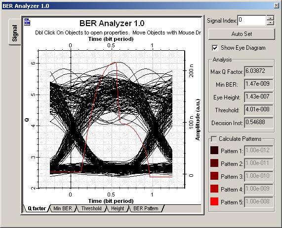
45 Select Electrical Amplifier 1.0 and place it onto the workspace by dragging the icon from the library. From the component library, go to Default > Filters Library > Electrical Select Low Pass Bessel Filter 1.0 and place it onto the workspace by dragging the icon from the library. Connect the first Demultiplexer output port to the Photodetector PIN, Connect the Photodetector output to the Electrical amplifier input, Connect the Electrical amplifier output to the Filter input. Set the electrical amplifier gain to 0 db. Figure 55 -Adding the receiver to the WDM system BER Analyzer In order to calculate the system performance you can use the BER Analyzer. This component can predict the BER, Q-factor, threshold and Eye aperture. You can also obtain the BER patterns and the BER value in each point of the Eye diagram using 3D graphs. From the component library, go to Default > Visualizers > Electrical Select BER Analyzer 1.0 and place it onto the workspace by dragging the icon from the library. The first input port of the BER Analyzer receives the binary signal. Connect the output of the first Pseudo-Random Bit Sequence Generator to the first input port of the BER Analyzer. 39

46 The second input port receives the original sampled signal, used to compensate the delay between the signals transmitted and the received. Connect the output of the first NRZ Pulse Generator to the second input port of the BER Analyzer. Connect the output port of the Electrical amplifier to third port of the BER Analyzer. Figure 56 -Connecting the BER Analyzer Run the simulation this simulation will take some time. Double-click in BER analyzer to display the results and graphs. Graphs and Results In the BER Analyzer, select the Show Eye Diagram option When opening the BER analyzer you will obtain the following graphs together with the Eye diagram: Q-Factor: this is the max value for the Q-Factor versus decision instant. Min BER: this is the min value for the BER versus decision instant. Threshold: this is the threshold value versus decision instant that gives the max Q-Factor and the min BER. Height: This is the Eye height for versus decision instant. BER Pattern: when enabled, shows the regions were the BER in the region is less than the user-defined values. 40

47 Figure 57 -BER Analyzer graphs You can also visualize the main results from these graphs in the Analysis frame: Maximum Q- Factor value, minimum BER value, maximum eye aperture, threshold and decision instant at the Max Q-Factor/ Min BER. Figure 58 -BER Analyzer results BER Patterns In order to calculate the BER patterns you must select the check box in the BER Analyzer display, or you can select the properties from the analyzer in the component. Select the BER Patterns check box the visualizer will recalculate the graphs and results In the BER analyzer display, select the BER patterns tab. 41


48 3D BER Graph Figure 59 -Calculating BER patterns In order to calculate the 3D BER, you must enable the calculation of the BER patterns and the 3D graph. Select the BER Analyzer icon in the layout, Right click on it, from the popup menu select Component properties Select the BER Patterns tab, Enable the parameters Calculate patterns and Calculate 3D graph. Press OK the visualizer will recalculate the graphs and results. Figure 60 -Calculating 3D graph 42


49 The 3D graph is available in the graphs tab of the project browser: In the Main menu, select View > Project Browser, or press Ctrl+2, In the project browser, select the Graphs tab, In the tree with components, select the BER Analyzer, Expand the tree and select the BER Pattern 3D Graph, Right click on it and from the pop up menu select Quick View Figure 61-3D graphs from the project browser 43

50 Lesson 4: Parameter Sweeps - BER x Input power The following procedure will show you how to combine the results from the BER/Eye Analyzer versus the signal input power using parameter sweeps. You will become familiar with parameter sweeps, graph builder, results, graphs and views. In this example we iterate the parameter Power at the CW Laser component. The file BER_InputPowerSweep.osd has the setup to generate the results; we will show the steps needed to follow in order to obtain these results in different designs. Figure 62 -Sample file that calculates BER x Input power 44
51 Selecting the parameter to be iterated using the Sweep mode First, we will select the parameter Power to be iterated using the parameter sweep feature. We want to be able to calculate the design using different values of the input power. Double click over the CW Laser component, In the Parameters dialog box, click on the Mode for the parameter Power Select the Sweep mode These steps are described in Figure 63: Figure 63 -Changing the parameter mode to Sweep First, we will select the parameter Power to be iterated using the parameter sweep feature. We want to be able to calculate the design using different values of the input power. 45


52 Changing the number of sweep iterations. In order to define the number of iterations sweep you must use the following procedure: Go to the Parameter Seeps Tab, In the Design Version menu, select Set Total Sweep Iterations Set the Total Iterations value to 10. These steps are described in Figure 64: Figure 64 -Adding iterations 46

53 Changing the values of sweep iterations. In the Parameter Sweeps tab you can enter the values directly in the table, or you can set the fist and the last value and use the Sweep iteration spread tool: In the Parameter Sweeps tab, enter the value for the Power in the first cell, -50 dbm, Enter the value for the Power in the last cell, 0 dbm, Select the entire table column, In the Tools menu, select Sweep Iterations Spread->Linear These steps are described in Figure 65: Figure 65 -Entering values for all iterations 47


54 Running the simulation From the File Menu select Calculate : Figure 66 - Running the simulation 48


55 Getting results using the Graph builder In order to create a graph showing the BER versus the power, you need to access the results generated by the BER Analyzer. In the Tools menu, select Graph Buider In the Graph builder tool, select the parameter Power from the CW Laser component in the X coordinate source area. Now select the results Min. BER from the BER Analyzer in the Y coordinate source area. Click on Add button, the graph will be added to the Graphs tab in the project browser. These steps are described in the Figure 68: Figure 67 -Building the graph 49

, In the Project Browser select the")


56 Graphs and Views After the simulation we built the graph to visualize the BER versus input power, this graph was added to the Graphs tab in the project browser, you can access this graph following this procedures. Open the Project Browser (Ctrl+2), In the Project Browser select the Graphs tab, In the graph tab, click over the Power vs. Min. BER, By right clicking over the graph name you can choose to show the graph using quick view or adding the graph to the Views tab. These steps are described in Figure 68: Ctrl+2 Graphs Figure 68 - Quick view and Adding to the views tab 50


57 Browsing parameter sweep iterations You can also open the BER visualizer and obtain the Eye diagrams and graphs such as Q factor and BER for different iterations changing the current sweep iteration. Double-click in the BER Analyzer, Select Show Eye Diagram, In the toolbar, change the Sweep iteration, Observe that for each iteration you will obtain different results, one for each value of input power. These steps are described in the Figure 70: Figure 69 -Browsing through the parameter sweep iterations, the Eye diagram, and Q-Factor for each value of laser power Combining graphs from sweep iterations Visualizer can generate graphs for all sweep iterations, however the visualizer will display only the current sweep iteration when the user accesses the graphs by double clinking on it and browse for different iterations. It s possible to access the graphs for all sweep iterations by using the Graph tab in the Project Browser. 51


58 Go to the Project Browser (Ctrl+2), Select the Graphs tab, In the Graphs tab, select the BER Analyzer 1.0 in the tree, Select the Q Factor graph, Right click on it, then select Add to view or Quick view Observe that you will obtain a display with the graphs for all sweep iterations, one for each value of input power. These steps are described in Figure 70: Figure 70 -Combining graphs from different sweep iterations in one graph 52


59 Lesson 5: Design Versions EDFA Characterization The sample file EDFA Characterization.osd shows how to use OptiSys_Design with multiple design versions. In this example we characterize the Erbium Doped Fiber Amplifier by using sweeps for the input parameters of the amplifier. Figure 71 -EDFA Characterization.osd This example use different parameter sweeps for each design version: Length: Iterations of EDFA fiber length from 1 to 20 meters. Input Signal Power: Iterations of CW laser signal power from -40 to 0 dbm Pump Power: Iterations of Pump laser power from 10 to 200 mw Wavelength: Iterations of CW laser signal wavelength from 1525 to 1600 nm Figure 72 -EDFA Multiple design versions and parameter sweeps 53


60 For each design version we have three graphs showing the Output signal power, Gain and Noise figure versus the sweep parameter. These three graphs were combined into one view, this means we have four views: Gain, Noise Figure and Output power versus Length, signal power, pump power and wavelength. Figure 73 -Graphs and Views 54

61 Lesson 6: Optimizations System margin OptiSys_Design can optimize parameters in order to maximize, minimize or to find the target value for results. This means you can optimize the fiber length of the EDFA to obtain the maximum gain, calculate the attenuation/gain to obtain a target Q-Factor, minimize the BER by optimizing the fiber length of the link, etc. The sample file System Margin.osd shows how to estimate the System margin; this margin shows the amount of power penalty that may be added to the system. The target BER is 10-9, that means a target Q-Factor of 6. Figure 74 -System Margin.osd In this example the subsystem System under test is an empty system. The optimization will optimize for the parameter attenuation from the Attenuator component to obtain the target value of the min Q-Factor from the BER Analyzer result. The parameter attenuation will be the system margin in db. 55


62 Figure 75 -Parameter optimizations You must enable the optimizations in the calculation dialog box in order to run the optimizations. Figure 76 -Enabling optimizations After the calculation the system margin value is around 38 db for a Q-Factor of 6. 56


63 Figure 77 -Getting results 57

64 Lesson 7: Optimizations EDFA Fiber length The sample file EDFA Fiber Length Optimization.osd shows how to maximize the gain optimizing the EDFA fiber length. Figure 78 - EDFA Fiber Length Optimization.osd In the Optimization tab, you can select the Optimization properties to access the parameters used for the optimization. In this example we search for the length of the fiber from 1 to 20 meters in order to maximize the gain measured from the WDM Dual Port Analyzer. 58


65 Figure 79 -Parameters for fiber length optimization You must enable the optimizations in the calculation dialog box in order to run the optimizations. In this example the maximum gain is 36 db, and the fiber length is 8 meters. Figure 80 -Results after calculation 59

66 Lesson 8: Dispersion compensation using subsystems and scripting This lesson will illustrate how to simulate a simple dispersion compensated link elaborating further the concepts of subsystem definition and scripting. Let us set up the following layout, which includes: Figure 81 -Dispersion compensated link span An abstract source of Gaussian RZ pulses according to a user defined bit sequence Booster amplifier and filter SMF and DCF Inline amplifier and filter Visualizers Let us examine the signal waveforms at the input, after the SMF and at the end of the span. One can observe that after the SMF the signal pulses are attenuated, broadened by a factor of approx. 2 and that there is considerable inter-symbol interference. 60


67 Input After SMF Output Figure 82 -Signal evolution in a dispersion compensated link span We can now use the powerful scripting feature of OptiSys in order to avoid the necessity to redefine those of the layout parameters that depend on the signal in case input signals change. One such parameter is the bandwidth of the two inline filters. Open the filter parameter dialog box and switch the Mode of the Bandwidth to Script. Right-click In the value field and select Bit rate. Then add 3 * so that the whole field reads 3 * Bit rate. Click on the layout workspace and show the Global parameters dialog. Increase twice the bit rate and calculate again. The following figure shows that regardless of the severe dispersive broadening in the SMF, the signal is again preserved after the whole span, both in terms of power and pulse shape. 61


68 After SMF Output Figure 83 -The results of the scripted calculations of a dispersion compensated link span Chances are that this single link might be useful for building longer multi-span systems. In that case it is recommended to encapsulate it into a sub-system, which would later on allow reproducing the same combination of components quickly and efficiently. We create a new design version, selecting Design Version/ Add Design Version from the main menu of OptiSys and change its name to Amplified Dispersion Compensating Subsystem. After that we copy and paste all the components of Version 1 in it. Next, as shown in Lesson 2: Subsystems Hierarchical simulation, we select all the components, except the signal source and the booster amplifier (including or skipping the visualizers), and select Create subsystem from the right click context menu. Our layout collapses into the visual representation of a subsystem. First we create an output port in the subsystem by selecting Look Inside from the right-click menu and using the Output port tool. After that we can change the name of the new subsystem to something informative, for instance Amplified Dispersion Compensated Span, using the Component Parameters menu item. 62


69 Figure 84 -The dispersion compensated span represented as a subsystem Next we can use the newly created subsystem to build longer multi-span links. Let us create another design version and change its name to Multi-Span Link. After that, we copy and paste all the components of Amplified Dispersion Compensating Subsystem in it. Now we can arrange a three span system by copying and pasting the Amplified Dispersion Compensated Span subsystem component and linking the respective input and output ports. Figure 85 -Building multi-span system using the user defined subsystem 63


70 Let us now define a more complex waveform and perform the calculation. After that we can display and compare the input and output signals in terms of their amplitude and pulse shape. Input Output Figure 86 - Input and output waveforms of the dispersion compensated links 64
 and L-band (1575-1610 nm).")
71 Lesson 9: Design of a broadband Raman amplifier using subsystems Overview The number of channels deployed in long-haul DWDM systems is rapidly increasing beyond hundreds of channels over the C-band ( nm) and L-band ( nm). This demand for more bandwidth is driving the search for new and more sophisticated fiber amplifiers that are flattened over a very wide spectral range for maximum bandwidth transmission over the long haul. The specifics of the stimulated Raman scattering effect allow for an interesting technique for gainflattening of broadband Raman amplifiers (Y. Emori, K. Tanaka and S. Namiki, Electron. Lett. 35, 1355, 1999). It requires only a suitable multiple-pump configuration and does not rely on passive filters, gratings, etc. Definition of Multi-line source At an initial stage of the pump system lets set up a group of twelve pump laser diodes having Parameterized signal representations and the following wavelengths and powers: LD λ [nm] P [mw] LD λ [nm] P [mw] After that we multiplex their outputs using, for instance, two multiplexers and a 2x1 power combiner. The channels of the multiplexers should be accordingly adjusted to the wavelengths of the pumps, as shown for the case of the 8x1 multiplexer: Figure 87 -Adjusting multiplexer channels 65


72 We arrive at the following layout and can now calculate and observe the compound output. Figure 88 - Multi-line source layout Definition of Multi-line source subsystem It would be handy to use that combination of elements for defining both the pumps and the signal sources of the broadband Raman amplifier. The easiest way to achieve this is to hide the details in a subsystem, which is to be used later for different applications with a minor tuning of the parameters. First we open a new design version named Multi-Line Sources. 66


73 After creating the subsystem as shown in Creating a Subsystem we copy and paste it two times. The two new instances of that subsystem will be used as signal sources in the region nm. Let us change the names of the subsystems respectively to Multi-Line Pump nm, Multi-Line Source nm and Multi-Line Source nm by double clicking their icons and filling the Label field in the parameter dialog box. Now we need to adjust the internal parameters of the two new subsystem instances in order to use them as signal sources. The following steps are the fastest way to do that: Right-click on the icon of Multi-Line Source nm Select Look inside from the context menu. The internal details are displayed in the layout editor. Open the Parameter groups by clicking Ctrl-5. In the Group drop-down list select Power, in the Units drop-down list select dbm Click on Value button to select all values in that column Right-click on Value and select Assign Multiple from the context menu. In the dialog box that pops up enter 10. Figure 89 - Rapidly adapting the parameters of a multi-line source 67


74 Next in the Group drop-down list select Frequency, in the Units drop-down list select nm Right-click on Value and select Spread from the context menu. In the dialog box that pops up enter 1510 for Start Value and 5.2 for Increment. Figure 90 - Rapidly tuning a multi-line source to a new spectral region Select Output Signal Type from Group. As described above Multiple Assign 0 to the Value of the Parameterized parameter. This means that the signals will be generated with full sampled spectra, using the sampled signal representation instead of the parameterized signal one. Close the subsystem. Repeat the same steps for the next subsystem setting its source wavelengths from to 1630 nm and the powers to 10 dbm Now we have the necessary pumps and signals and can start building the Raman amplifier 68

75 Figure 91 Raman Amplifier subsystems Designing a broadband gain-flattened Raman amplifier First we open a new design version named Broadband Raman Amplifier. Then we copy and paste all the subsystems from the previous design version into the new one. After adding the Raman amplifier component from the Amplifiers component library, 2x1 combiner and several OSA visualizers we arrive at the following layout: 69
76 Figure 92 - Broadband gain-flattened Raman amplifier layout For the properties of the amplifier fiber we enter the typical values of a SMF-28 fiber and set its length to 40 km. Everything is now set and we start the calculation of the current design version only. When it is finished we can display and analyse the signal spectra at different points of the system for example the output powers: 70

77 Figure 93 - Forward output spectrum of the amplified signals and the backscattered pump It is seen that the gain of the device is relatively flat in a broad spectral region. The next lesson will show how to improve that feature further by using the optimization tools of OptiSys_Design. Using the interactive 3D graphics The Raman amplifier component provides rich visual information in the form of 3D surfaces that are interactive in real time. These 3D plots show the evolution along the fiber length of the following important characteristics of the device: Signal power spectrum Gain spectrum Gain coefficient spectrum Noise figure spectrum Double Rayleigh scattering spectrum Two 3D graphs of each type are supported for the forward and backward propagating signals respectively. The following picture shows the evolution of the gain experienced by the forward propagating waves. The high gain of the ASE in the shorter wavelength region (right) is due to the fact that it experiences both Rayleigh and stimulated Raman scattering in the field of the strong pumps. 71

78 On the other hand it is clearly seen that the combined Raman amplification almost perfectly compensates for the fiber losses along the full length of the amplifier. Figure 94 - The longitudinal evolution of the forward gain spectrum in the broadband gainflattened Raman amplifier 72
79 Lesson 10: Optimization of the gain flatness of broadband Raman amplifiers The flatness of the gain of inline fiber amplifiers is a matter of primary importance for WDM systems. This lesson will demonstrate how to optimize further the gain uniformity of the Raman amplifier described in Lesson 9: Design of a broadband Raman amplifier using subsystems. There are numerous parameters that influence considerably the performance of Raman amplifiers, but the most easily controlled one is probably the fiber length. Optimizing the length of the fiber First we set the mode of the parameter Fiber Length to Sweep. Next we adjust the number of iterations to 13 by using the sequence of steps described in Changing the number of sweep iterations. Next we define range of values for the fiber length from 10 to 40 km, as shown in Changing the values of sweep iterations. Figure 95 - Sweeping the length of the broadband gain-flattened Raman amplifier Next we have to add the Results Maximal Forward Gain [db] and Forward Gain Flatness [db] to the results display table as shown in the following figure: 73


80 Figure 96 - Selecting results Now we perform the calculations by checking Calculate all iterations in current design version. When finished the Results tab window contains the respective values of the two results as a function of the parametrically swept fiber length. Figure 97 - The results as a function of the parametrically swept fiber length 74


81 It is immediately seen that optimal gain flatness of < 1 db can be achieved using fiber lengths of approximately 25 km. The influence of fiber losses In the case of nonlinear devices like that broadband Raman amplifier it is not always true that less background fiber losses assure better performance. In order to determine quantitatively the influence of this parameter on the gain flatness of the amplifier we can perform another sweeping calculation. Let the values of attenuation vary in the range db/km. Figure 98 - Sweeping the fiber attenuation After the calculation we get the following results, which show that the optimal flatness and small positive gain correspond to attenuation coefficient of db/km. Figure 99 - The results as a function of the parametrically swept fiber attenuation 75

82 It is informative also to display and analyse the superimposed forward output gain spectra obtained for the different values of the attenuation as shown in the following figure: Figure Forward output gain spectra as depending on the attenuation of the fiber 76
Application of optical system simulation software in a fiber optic telecommunications program
 Rochester Institute of Technology RIT Scholar Works Presentations and other scholarship 2004 Application of optical system simulation software in a fiber optic telecommunications program Warren Koontz
CHAPTER 4 RESULTS. 4.1 Introduction
 CHAPTER 4 RESULTS 4.1 Introduction In this chapter focus are given more on WDM system. The results which are obtained mainly from the simulation work are presented. In simulation analysis, the study will
Performance Limitations of WDM Optical Transmission System Due to Cross-Phase Modulation in Presence of Chromatic Dispersion
 Performance Limitations of WDM Optical Transmission System Due to Cross-Phase Modulation in Presence of Chromatic Dispersion M. A. Khayer Azad and M. S. Islam Institute of Information and Communication
OptiSystem Getting Started
 OptiSystem Getting Started Optical Communication System Design Software Version 7.0 for Windows XP/Vista OptiSystem Getting Started Optical Communication System Design Software Copyright 2008 Optiwave
Chirped Bragg Grating Dispersion Compensation in Dense Wavelength Division Multiplexing Optical Long-Haul Networks
 363 Chirped Bragg Grating Dispersion Compensation in Dense Wavelength Division Multiplexing Optical Long-Haul Networks CHAOUI Fahd 3, HAJAJI Anas 1, AGHZOUT Otman 2,4, CHAKKOUR Mounia 3, EL YAKHLOUFI Mounir
Implementing of High Capacity Tbps DWDM System Optical Network
 , pp. 211-218 http://dx.doi.org/10.14257/ijfgcn.2016.9.6.20 Implementing of High Capacity Tbps DWDM System Optical Network Daleep Singh Sekhon *, Harmandar Kaur Deptt.of ECE, GNDU Regional Campus, Jalandhar,Punjab,India
RZ BASED DISPERSION COMPENSATION TECHNIQUE IN DWDM SYSTEM FOR BROADBAND SPECTRUM
 RZ BASED DISPERSION COMPENSATION TECHNIQUE IN DWDM SYSTEM FOR BROADBAND SPECTRUM Prof. Muthumani 1, Mr. Ayyanar 2 1 Professor and HOD, 2 UG Student, Department of Electronics and Communication Engineering,
OptiSystem. Optical Communication System and Amplifier Design Software
 4 Specific Benefits Overview In an industry where cost effectiveness and productivity are imperative for success, the award winning OptiSystem can minimize time requirements and decrease cost related to
OptiSystem. Optical Communication System and Amplifier Design Software
 SPECIFIC BENEFITS OVERVIEW In an industry where cost effectiveness and productivity are imperative for success, the award winning can minimize time requirements and decrease cost related to the design
Performance Comparison of Pre-, Post-, and Symmetrical Dispersion Compensation for 96 x 40 Gb/s DWDM System using DCF
 Performance Comparison of Pre-, Post-, and Symmetrical Dispersion Compensation for 96 x 40 Gb/s DWDM System using Sabina #1, Manpreet Kaur *2 # M.Tech(Scholar) & Department of Electronics & Communication
Key Features for OptiSystem 12
 12 New Features Created to address the needs of research scientists, optical telecom engineers, professors and students, OptiSystem satisfies the demand of users who are searching for a powerful yet easy
Performance Evaluation of 32 Channel DWDM System Using Dispersion Compensation Unit at Different Bit Rates
 Performance Evaluation of 32 Channel DWDM System Using Dispersion Compensation Unit at Different Bit Rates Simarpreet Kaur Gill 1, Gurinder Kaur 2 1Mtech Student, ECE Department, Rayat- Bahra University,
Analysis of four channel CWDM Transceiver Modules based on Extinction Ratio and with the use of EDFA
 Analysis of four channel CWDM Transceiver Modules based on Extinction Ratio and with the use of EDFA P.P. Hema [1], Prof. A.Sangeetha [2] School of Electronics Engineering [SENSE], VIT University, Vellore
PERFORMANCE ANALYSIS OF OPTICAL TRANSMISSION SYSTEM USING FBG AND BESSEL FILTERS
 PERFORMANCE ANALYSIS OF OPTICAL TRANSMISSION SYSTEM USING FBG AND BESSEL FILTERS Antony J. S., Jacob Stephen and Aarthi G. ECE Department, School of Electronics Engineering, VIT University, Vellore, Tamil
Compensation of Dispersion in 10 Gbps WDM System by Using Fiber Bragg Grating
 International Journal of Computational Engineering & Management, Vol. 15 Issue 5, September 2012 www..org 16 Compensation of Dispersion in 10 Gbps WDM System by Using Fiber Bragg Grating P. K. Raghav 1,
SIMULATIVE INVESTIGATION OF SINGLE-TONE ROF SYSTEM USING VARIOUS DUOBINARY MODULATION FORMATS
 SIMULATIVE INVESTIGATION OF SINGLE-TONE ROF SYSTEM USING VARIOUS DUOBINARY MODULATION FORMATS Namita Kathpal 1 and Amit Kumar Garg 2 1,2 Department of Electronics & Communication Engineering, Deenbandhu
Performance Analysis of dispersion compensation using Fiber Bragg Grating (FBG) in Optical Communication
 in Optical Communication") Research Article International Journal of Current Engineering and Technology E-ISSN 2277 416, P-ISSN 2347-5161 214 INPRESSCO, All Rights Reserved Available at http://inpressco.com/category/ijcet Performance
Research Article International Journal of Current Engineering and Technology E-ISSN 2277 416, P-ISSN 2347-5161 214 INPRESSCO, All Rights Reserved Available at http://inpressco.com/category/ijcet Performance
Optical Transport Tutorial
 Optical Transport Tutorial 4 February 2015 2015 OpticalCloudInfra Proprietary 1 Content Optical Transport Basics Assessment of Optical Communication Quality Bit Error Rate and Q Factor Wavelength Division
Design of an Optical Submarine Network With Longer Range And Higher Bandwidth
 Design of an Optical Submarine Network With Longer Range And Higher Bandwidth Yashas Joshi 1, Smridh Malhotra 2 1,2School of Electronics Engineering (SENSE) Vellore Institute of Technology Vellore, India
5 GBPS Data Rate Transmission in a WDM Network using DCF with FBG for Dispersion Compensation
 ABHIYANTRIKI 5 GBPS Data Rate Meher et al. An International Journal of Engineering & Technology (A Peer Reviewed & Indexed Journal) Vol. 4, No. 4 (April, 2017) http://www.aijet.in/ eissn: 2394-627X 5 GBPS
DISPERSION COMPENSATION IN OFC USING FBG
 DISPERSION COMPENSATION IN OFC USING FBG 1 B.GEETHA RANI, 2 CH.PRANAVI 1 Asst. Professor, Dept. of Electronics and Communication Engineering G.Pullaiah College of Engineering Kurnool, Andhra Pradesh billakantigeetha@gmail.com
The secondary MZM used to modulate the quadrature phase carrier produces a phase shifted version:
 QAM Receiver 1 OBJECTIVE Build a coherent receiver based on the 90 degree optical hybrid and further investigate the QAM format. 2 PRE-LAB In the Modulation Formats QAM Transmitters laboratory, a method
Key Features for OptiSystem 14
 14.0 New Features Created to address the needs of research scientists, photonic engineers, professors and students; OptiSystem satisfies the demand of users who are searching for a powerful yet easy to
QAM Transmitter 1 OBJECTIVE 2 PRE-LAB. Investigate the method for measuring the BER accurately and the distortions present in coherent modulators.
 QAM Transmitter 1 OBJECTIVE Investigate the method for measuring the BER accurately and the distortions present in coherent modulators. 2 PRE-LAB The goal of optical communication systems is to transmit
Phase Modulator for Higher Order Dispersion Compensation in Optical OFDM System
 Phase Modulator for Higher Order Dispersion Compensation in Optical OFDM System Manpreet Singh 1, Karamjit Kaur 2 Student, University College of Engineering, Punjabi University, Patiala, India 1. Assistant
OFC SYSTEMS Performance & Simulations. BC Choudhary NITTTR, Sector 26, Chandigarh
 OFC SYSTEMS Performance & Simulations BC Choudhary NITTTR, Sector 26, Chandigarh High Capacity DWDM OFC Link Capacity of carrying enormous rates of information in THz 1.1 Tb/s over 150 km ; 55 wavelengths
Optimized Dispersion Compensation with Post Fiber Bragg Grating in WDM Optical Network
 International Journal of Scientific & Engineering Research, Volume 3, Issue 10, October-2012 1 Optimized Dispersion Compensation with Post Fiber Bragg Grating in WDM Optical Network P.K. Raghav, M. P.
Introduction to Simulink Assignment Companion Document
 Introduction to Simulink Assignment Companion Document Implementing a DSB-SC AM Modulator in Simulink The purpose of this exercise is to explore SIMULINK by implementing a DSB-SC AM modulator. DSB-SC AM
Dr. Monir Hossen ECE, KUET
 Dr. Monir Hossen ECE, KUET 1 Outlines of the Class Principles of WDM DWDM, CWDM, Bidirectional WDM Components of WDM AWG, filter Problems with WDM Four-wave mixing Stimulated Brillouin scattering WDM Network
Implementation of Dense Wavelength Division Multiplexing FBG
 AUSTRALIAN JOURNAL OF BASIC AND APPLIED SCIENCES ISSN:1991-8178 EISSN: 2309-8414 Journal home page: www.ajbasweb.com Implementation of Dense Wavelength Division Multiplexing Network with FBG 1 J. Sharmila
PERFORMANCE ANALYSIS OF WDM AND EDFA IN C-BAND FOR OPTICAL COMMUNICATION SYSTEM
 www.arpapress.com/volumes/vol13issue1/ijrras_13_1_26.pdf PERFORMANCE ANALYSIS OF WDM AND EDFA IN C-BAND FOR OPTICAL COMMUNICATION SYSTEM M.M. Ismail, M.A. Othman, H.A. Sulaiman, M.H. Misran & M.A. Meor
Improved Analysis of Hybrid Optical Amplifier in CWDM System
 Improved Analysis of Hybrid Optical Amplifier in CWDM System 1 Bandana Mallick, 2 Reeta Kumari, 3 Anirban Mukherjee, 4 Kunwar Parakram 1. Asst Proffesor in Dept. of ECE, GIET Gunupur 2, 3,4. Student in
Comparative Analysis Of Different Dispersion Compensation Techniques On 40 Gbps Dwdm System
 INTERNATIONAL JOURNAL OF TECHNOLOGY ENHANCEMENTS AND EMERGING ENGINEERING RESEARCH, VOL 3, ISSUE 06 34 Comparative Analysis Of Different Dispersion Compensation Techniques On 40 Gbps Dwdm System Meenakshi,
Performance Analysis Of Hybrid Optical OFDM System With High Order Dispersion Compensation
 Performance Analysis Of Hybrid Optical OFDM System With High Order Dispersion Compensation Manpreet Singh Student, University College of Engineering, Punjabi University, Patiala, India. Abstract Orthogonal
interpolation and smoothing filter options. New graph display OFDM FFT of subcarrier indexes.
 What s New in 9.0 Created to address the needs of research scientists, optical telecom engineers, professors and students, OptiSystem satisfies the demand of users who are searching for a powerful yet
Available online at ScienceDirect. Procedia Computer Science 93 (2016 )
") Available online at www.sciencedirect.com ScienceDirect Procedia Computer Science 93 (016 ) 647 654 6th International Conference On Advances In Computing & Communications, ICACC 016, 6-8 September 016,
Available online at www.sciencedirect.com ScienceDirect Procedia Computer Science 93 (016 ) 647 654 6th International Conference On Advances In Computing & Communications, ICACC 016, 6-8 September 016,
Enhancing Optical Network Capacity using DWDM System and Dispersion Compansating Technique
 ISSN (Print) : 2320 3765 ISSN (Online): 2278 8875 International Journal of Advanced Research in Electrical, Electronics and Instrumentation Engineering Vol. 6, Issue 12, December 2017 Enhancing Optical
Matlab component Creating a component to handle optical signals. OptiSystem Application Note
 Matlab component Creating a component to handle optical signals OptiSystem Application Note Matlab component Creating a component to handle optical signals 1. Optical Attenuator Component In order to create
ANALYSIS OF FWM POWER AND EFFICIENCY IN DWDM SYSTEMS BASED ON CHROMATIC DISPERSION AND CHANNEL SPACING
 ANALYSIS OF FWM POWER AND EFFICIENCY IN DWDM SYSTEMS BASED ON CHROMATIC DISPERSION AND CHANNEL SPACING S Sugumaran 1, Manu Agarwal 2, P Arulmozhivarman 3 School of Electronics Engineering, VIT University,
International Journal of Advanced Research in Computer Science and Software Engineering
 ISSN: 2277 128X International Journal of Advanced Research in Computer Science and Software Engineering Research Paper Available online at: Performance Analysis of WDM/SCM System Using EDFA Mukesh Kumar
A Novel Design Technique for 32-Channel DWDM system with Hybrid Amplifier and DCF
 Research Manuscript Title A Novel Design Technique for 32-Channel DWDM system with Hybrid Amplifier and DCF Dr.Punal M.Arabi, Nija.P.S PG Scholar, Professor, Department of ECE, SNS College of Technology,
Photonics (OPTI 510R 2017) - Final exam. (May 8, 10:30am-12:30pm, R307)
 - Final exam. (May 8, 10:30am-12:30pm, R307)") Photonics (OPTI 510R 2017) - Final exam (May 8, 10:30am-12:30pm, R307) Problem 1: (30pts) You are tasked with building a high speed fiber communication link between San Francisco and Tokyo (Japan) which
Photonics (OPTI 510R 2017) - Final exam (May 8, 10:30am-12:30pm, R307) Problem 1: (30pts) You are tasked with building a high speed fiber communication link between San Francisco and Tokyo (Japan) which
Performance Investigation of RAMAN-EDFA HOA for DWDM System (Received 17 September, 2016 Accepted 02 October, 2016)
") Performance Investigation of RAMAN-EDFA HOA for DWDM System (Received 17 September, 2016 Accepted 02 October, 2016) ABSTRACT Neha Thakral Research Scholar, DAVIET, Jalandhar nthakral9@gmail.com Earlier
Performance Investigation of RAMAN-EDFA HOA for DWDM System (Received 17 September, 2016 Accepted 02 October, 2016) ABSTRACT Neha Thakral Research Scholar, DAVIET, Jalandhar nthakral9@gmail.com Earlier
32-Channel DWDM System Design and Simulation by Using EDFA with DCF and Raman Amplifiers
 2012 International Conference on Information and Computer Networks (ICICN 2012) IPCSIT vol. 27 (2012) (2012) IACSIT Press, Singapore 32-Channel DWDM System Design and Simulation by Using EDFA with DCF
Design of Ultra High Capacity DWDM System with Different Modulation Formats
 Design of Ultra High Capacity DWDM System with Different Modulation Formats A. Nandhini 1, K. Gokulakrishnan 2 1 PG Scholar, Department of Electronics & Communication Engineering, Regional Center, Anna
Performance Evaluation of Hybrid (Raman+EDFA) Optical Amplifiers in Dense Wavelength Division Multiplexed Optical Transmission System
 Optical Amplifiers in Dense Wavelength Division Multiplexed Optical Transmission System") Performance Evaluation of Hybrid (Raman+EDFA) Optical Amplifiers in Dense Wavelength Division Multiplexed Optical Transmission System Gagandeep Singh Walia 1, Kulwinder Singh 2, Manjit Singh Bhamrah 3
Performance Evaluation of Hybrid (Raman+EDFA) Optical Amplifiers in Dense Wavelength Division Multiplexed Optical Transmission System Gagandeep Singh Walia 1, Kulwinder Singh 2, Manjit Singh Bhamrah 3
Performance of A Multicast DWDM Network Applied to the Yemen Universities Network using Quality Check Algorithm
 Performance of A Multicast DWDM Network Applied to the Yemen Universities Network using Quality Check Algorithm Khaled O. Basulaim, Samah Ali Al-Azani Dept. of Information Technology Faculty of Engineering,
Simulative Analysis of 40 Gbps DWDM System Using Combination of Hybrid Modulators and Optical Filters for Suppression of Four-Wave Mixing
 Vol.9, No.7 (2016), pp.213-220 http://dx.doi.org/10.14257/ijsip.2016.9.7.18 Simulative Analysis of 40 Gbps DWDM System Using Combination of Hybrid Modulators and Optical Filters for Suppression of Four-Wave
40Gb/s Optical Transmission System Testbed
 The University of Kansas Technical Report 40Gb/s Optical Transmission System Testbed Ron Hui, Sen Zhang, Ashvini Ganesh, Chris Allen and Ken Demarest ITTC-FY2004-TR-22738-01 January 2004 Sponsor: Sprint
PERFORMANCE ANALYSIS OF 4 CHANNEL WDM_EDFA SYSTEM WITH GAIN EQUALISATION
 PERFORMANCE ANALYSIS OF 4 CHANNEL WDM_EDFA SYSTEM WITH GAIN EQUALISATION S.Hemalatha 1, M.Methini 2 M.E.Student, Department Of ECE, Sri Sairam Engineering College,Chennai,India1 Assistant professsor,department
Eye-Diagram-Based Evaluation of RZ and NRZ Modulation Methods in a 10-Gb/s Single-Channel and a 160-Gb/s WDM Optical Networks
 International Journal of Optics and Applications 2017, 7(2): 31-36 DOI: 10.5923/j.optics.20170702.01 Eye-Diagram-Based Evaluation of RZ and NRZ Modulation Methods in a 10-Gb/s Single-Channel and a 160-Gb/s
Analysis of Self Phase Modulation Fiber nonlinearity in Optical Transmission System with Dispersion
 36 Analysis of Self Phase Modulation Fiber nonlinearity in Optical Transmission System with Dispersion Supreet Singh 1, Kulwinder Singh 2 1 Department of Electronics and Communication Engineering, Punjabi
Key Features for OptiSystem 14.2
 14.2 New Features Created to address the needs of research scientists, photonic engineers, professors and students; OptiSystem satisfies the demand of users who are searching for a powerful yet easy to
Chapter 3 Metro Network Simulation
 Chapter 3 Metro Network Simulation 3.1 Photonic Simulation Tools Simulation of photonic system has become a necessity due to the complex interactions within and between components. Tools have evolved from
UNIVERSITY OF TORONTO FACULTY OF APPLIED SCIENCE AND ENGINEERING. FINAL EXAMINATION, April 2017 DURATION: 2.5 hours
 UNIVERSITY OF TORONTO FACULTY OF APPLIED SCIENCE AND ENGINEERING ECE4691-111 S - FINAL EXAMINATION, April 2017 DURATION: 2.5 hours Optical Communication and Networks Calculator Type: 2 Exam Type: X Examiner:
Design and Performance Analysis of Optical Transmission System
 IOSR Journal of Engineering (IOSRJEN) ISSN (e): 2250-3021, ISSN (p): 2278-8719 Vol. 04, Issue 05 (May. 2014), V3 PP 22-26 www.iosrjen.org Design and Performance Analysis of Optical Transmission System
Optiva RF-Over-Fiber Design Tool User s Guide. Revision 1.0 March 27, 2015
 Optiva RF-Over-Fiber Design Tool User s Guide Revision 1.0 March 27, 2015 2015 Jenco Technologies Inc. All rights reserved. Every attempt has been made to make this material complete, accurate, and up-to-date.
Improvisation of Gain and Bit-Error Rate for an EDFA-WDM System using Different Filters
 Improvisation of Gain and Bit-Error Rate for an EDFA-WDM System using Different Filters Sharmila M M.Tech LEOE Department of physics College of engineering guindy Chennai 600025 India. Abstract: The Gain
International Journal Of Scientific Research And Education Volume 3 Issue 4 Pages April-2015 ISSN (e): Website:
: Website:") International Journal Of Scientific Research And Education Volume 3 Issue 4 Pages-3183-3188 April-2015 ISSN (e): 2321-7545 Website: http://ijsae.in Effects of Four Wave Mixing (FWM) on Optical Fiber in
International Journal Of Scientific Research And Education Volume 3 Issue 4 Pages-3183-3188 April-2015 ISSN (e): 2321-7545 Website: http://ijsae.in Effects of Four Wave Mixing (FWM) on Optical Fiber in
Kuldeep Kaur #1, Gurpreet Bharti *2
 Performance Evaluation of Hybrid Optical Amplifier in Different Bands for DWDM System Kuldeep Kaur #1, Gurpreet Bharti *2 #1 M Tech Student, E.C.E. Department, YCOE, Talwandi Sabo, Punjabi University,
International Journal of Computational Intelligence and Informatics, Vol. 2: No. 4, January - March Bandwidth of 13GHz
 Simulation and Analysis of GFF at WDM Mux Bandwidth of 13GHz Warsha Balani Department of ECE, BIST Bhopal, India balani.warsha@gmail.com Manish Saxena Department of ECE,BIST Bhopal, India manish.saxena2008@gmail.com
Performance Investigation of Dispersion Compensation Techniques in 32-Channel DWDM System
 Performance Investigation of Dispersion Compensation Techniques in 32-Channel DWDM System Deepak Sharma ECE Department, UIET, MDU Rohtak Payal ECE Department, UIET, MDU Rohtak Rajbir Singh ECE Department,
EDFA Applications in Test & Measurement
 EDFA Applications in Test & Measurement White Paper PN 200-0600-00 Revision 1.1 September 2003 Calmar Optcom, Inc www.calamropt.com Overview Erbium doped fiber amplifiers (EDFAs) amplify optical pulses
Simulation of Pre & Post Compensation Techniques for 16 Channels DWDM Optical Network using CSRZ & DRZ Formats
 Simulation of Pre & Post Compensation Techniques for 16 Channels DWDM Optical Network using CSRZ & DRZ Formats Richa Arya 1, Malti Rani 2 1 M. Tech, Computer Science Department, Punjab Technical University,
CHAPTER 5 SPECTRAL EFFICIENCY IN DWDM
 61 CHAPTER 5 SPECTRAL EFFICIENCY IN DWDM 5.1 SPECTRAL EFFICIENCY IN DWDM Due to the ever-expanding Internet data traffic, telecommunication networks are witnessing a demand for high-speed data transfer.
Enhanced continuous-wave four-wave mixing using Hybrid Modulation Technique
 International Journal of Current Engineering and Technology E-ISSN 2277 4106, P-ISSN 2347 5161 2016 INPRESSCO, All Rights Reserved Available at http://inpressco.com/category/ijcet Research Article Enhanced
EDFA-WDM Optical Network Analysis
 EDFA-WDM Optical Network Analysis Narruvala Lokesh, kranthi Kumar Katam,Prof. Jabeena A Vellore Institute of Technology VIT University, Vellore, India Abstract : Optical network that apply wavelength division
Ultra-long Span Repeaterless Transmission System Technologies
 Ultra-long Span Repeaterless Transmission System Technologies INADA Yoshihisa Abstract The recent increased traffic accompanying the rapid dissemination of broadband communications has been increasing
Performance Analysis of Dispersion Compensation using FBG and DCF in WDM Systems
 Performance Analysis of Dispersion using FBG and DCF in WDM Systems Ranjana Rao 1 Dr. Suresh Kumar 2 1 M. Tech Scholar, ECE Deptt UIET MDU Rohtak, Haryana, India 2 Assistant Professor, ECE Deptt, UIET
Introduction to BER testing of WDM systems
 Introduction to BER testing of WDM systems Application note 1299 Wavelength division multiplexing (WDM) is a new and exciting technology for migrating the core optical transmission network to higher bandwidths.
ECEN689: Special Topics in Optical Interconnects Circuits and Systems Spring 2016
 ECEN689: Special Topics in Optical Interconnects Circuits and Systems Spring 016 Lecture 7: Transmitter Analysis Sam Palermo Analog & Mixed-Signal Center Texas A&M University Optical Modulation Techniques
FWM Suppression in WDM Systems Using Advanced Modulation Formats
 FWM Suppression in WDM Systems Using Advanced Modulation Formats M.M. Ibrahim (eng.mohamed.ibrahim@gmail.com) and Moustafa H. Aly (drmosaly@gmail.com) OSA Member Arab Academy for Science, Technology and
Performance Evaluation of Different Hybrid Optical Amplifiers for 64 10, and Gbps DWDM transmission system
 Performance Evaluation of Different Hybrid Optical Amplifiers for 64 10, 96 10 and 128 10 Gbps DWDM transmission system Rashmi a, Anurag Sharma b, Vikrant Sharma c a Deptt. of Electronics & Communication
Performance Evaluation of Post and Symmetrical DCF Technique with EDFA in 32x10, 32x20 and 32x40 Gbps WDM Systems
 International Journal of Current Engineering and Technology E-ISSN 2277 4106, P-ISSN 2347 5161 2017 INPRESSCO, All Rights Reserved Available at http://inpressco.com/category/ijcet Research Article Performance
OFC SYSTEM: Design & Analysis. BC Choudhary, Professor NITTTR, Sector 26, Chandigarh.
 OFC SYSTEM: Design & Analysis BC Choudhary, Professor NITTTR, Sector 26, Chandigarh. OFC point-to-point Link Transmitter Electrical to Optical Conversion Coupler Optical Fiber Coupler Optical to Electrical
Agilent 83430A Lightwave Digital Source Product Overview
 Agilent Lightwave Digital Source Product Overview SDH/SONET Compliant DFB laser source for digital, WDM, and analog test up to 2.5 Gb/s 52 Mb/s STM-0/OC-1 155 Mb/s STM-1/OC-3 622 Mb/s STM-4/OC-12 2488
Performance Analysis of Gb/s DWDM Metropolitan Area Network using SMF-28 and MetroCor Optical Fibres
 Research Cell: An International Journal of Engineering Sciences ISSN: 2229-6913 Issue Sept 2011, Vol. 4 11 Performance Analysis of 32 2.5 Gb/s DWDM Metropolitan Area Network using SMF-28 and MetroCor Optical
Optical Fiber Technology
 Optical Fiber Technology 18 (2012) 29 33 Contents lists available at SciVerse ScienceDirect Optical Fiber Technology www.elsevier.com/locate/yofte A novel WDM passive optical network architecture supporting
Spectral Response of FWM in EDFA for Long-haul Optical Communication
 Spectral Response of FWM in EDFA for Long-haul Optical Communication Lekshmi.S.R 1, Sindhu.N 2 1 P.G.Scholar, Govt. Engineering College, Wayanad, Kerala, India 2 Assistant Professor, Govt. Engineering
Agilent 81980/ 81940A, Agilent 81989/ 81949A, Agilent 81944A Compact Tunable Laser Sources
 Agilent 81980/ 81940A, Agilent 81989/ 81949A, Agilent 81944A Compact Tunable Laser Sources December 2004 Agilent s Series 819xxA high-power compact tunable lasers enable optical device characterization
Simulation of RoF Using Wavelength Selective OADM
 International Journal of Research Studies in Science, Engineering and Technology Volume 2, Issue 9, September 2015, PP 16-22 ISSN 2349-4751 (Print) & ISSN 2349-476X (Online) Simulation of RoF Using Wavelength
Elements of Optical Networking
 Bruckner Elements of Optical Networking Basics and practice of optical data communication With 217 Figures, 13 Tables and 93 Exercises Translated by Patricia Joliet VIEWEG+ TEUBNER VII Content Preface
Determination of ideal Fibre Bragg Grating (FBG) length for Optical Transmission System
 length for Optical Transmission System") Determination of ideal Fibre Bragg Grating (FBG) length for Optical Transmission System Aastha Singhal SENSE school, VIT University Vellore, India Akanksha Singh SENSE school, VIT University Vellore, India
Determination of ideal Fibre Bragg Grating (FBG) length for Optical Transmission System Aastha Singhal SENSE school, VIT University Vellore, India Akanksha Singh SENSE school, VIT University Vellore, India
AirScope Spectrum Analyzer User s Manual
 AirScope Spectrum Analyzer Manual Revision 1.0 October 2017 ESTeem Industrial Wireless Solutions Author: Date: Name: Eric P. Marske Title: Product Manager Approved by: Date: Name: Michael Eller Title:
OPTICAL NETWORKS. Building Blocks. A. Gençata İTÜ, Dept. Computer Engineering 2005
 OPTICAL NETWORKS Building Blocks A. Gençata İTÜ, Dept. Computer Engineering 2005 Introduction An introduction to WDM devices. optical fiber optical couplers optical receivers optical filters optical amplifiers
40Gb/s Coherent DP-PSK for Submarine Applications
 4Gb/s Coherent DP-PSK for Submarine Applications Jamie Gaudette, Elizabeth Rivera Hartling, Mark Hinds, John Sitch, Robert Hadaway Email: Nortel, 3 Carling Ave., Ottawa, ON, Canada
Department of Electrical and Computer Systems Engineering
 Department of Electrical and Computer Systems Engineering Technical Report MECSE-4-2005 DWDM Optically Amplified Transmission Systems - SIMULINK Models and Test-Bed: Part III DPSK L.N. Binh and Y.L.Cheung
Implementation and analysis of 2 Tbps MDRZ DWDM system at ultra narrow channel spacing
 Implementation and analysis of 2 Tbps MDRZ DWDM system at ultra narrow channel spacing 1 Ragini Sharma, 2 Kamaldeep Kaur 1 Student, 2 Assistant Professor Department of Electrical Engineering BBSBEC, Fatehgarh
Analysis of Transmitting 40Gb/s CWDM Based on Extinction Value and Fiber Length Using EDFA
 IOSR Journal of Engineering (IOSRJEN) ISSN (e): 2250-3021, ISSN (p): 2278-8719 Vol. 04, Issue 02 (February. 2014), V6 PP 46-52 www.iosrjen.org Analysis of Transmitting 40Gb/s CWDM Based on Extinction Value
Performance Analysis of WDM RoF-EPON Link with and without DCF and FBG
 Optics and Photonics Journal, 2013, 3, 163-168 http://dx.doi.org/10.4236/opj.2013.32027 Published Online June 2013 (http://www.scirp.org/journal/opj) Performance Analysis of WDM RoF-EPON Link with and
Wavelength Interleaving Based Dispersion Tolerant RoF System with Double Sideband Carrier Suppression
 Wavelength Interleaving Based Dispersion Tolerant RoF System with Double Sideband Carrier Suppression Hilal Ahmad Sheikh 1, Anurag Sharma 2 1 (Dept. of Electronics & Communication, CTITR, Jalandhar, India)
Module 19 : WDM Components
 Module 19 : WDM Components Lecture : WDM Components - I Part - I Objectives In this lecture you will learn the following WDM Components Optical Couplers Optical Amplifiers Multiplexers (MUX) Insertion
Optical Transport Technologies and Trends
 Optical Transport Technologies and Trends A Network Planning Perspective Sept 1, 2014 Dion Leung, Director of Solutions and Sales Engineering dleung@btisystem.com About BTI Customers 380+ worldwide in
Performance Analysis of WDM-FSO Link under Turbulence Channel
 Available online at www.worldscientificnews.com WSN 50 (2016) 160-173 EISSN 2392-2192 Performance Analysis of WDM-FSO Link under Turbulence Channel Mazin Ali A. Ali Department of Physics, College of Science,
Ansoft Designer Tutorial ECE 584 October, 2004
 Ansoft Designer Tutorial ECE 584 October, 2004 This tutorial will serve as an introduction to the Ansoft Designer Microwave CAD package by stepping through a simple design problem. Please note that there
Q8384 Q8384. Optical Spectrum Analyzer
 Q8384 Optical Spectrum Analyzer Can measure and evaluate ultra high-speed optical DWDM transmission systems, and optical components at high wavelength resolution and high accuracy. New high-end optical
Optical Fibre Amplifiers Continued
 1 Optical Fibre Amplifiers Continued Stavros Iezekiel Department of Electrical and Computer Engineering University of Cyprus ECE 445 Lecture 09 Fall Semester 2016 2 ERBIUM-DOPED FIBRE AMPLIFIERS BASIC
S Optical Networks Course Lecture 4: Transmission System Engineering
 S-72.3340 Optical Networks Course Lecture 4: Transmission System Engineering Edward Mutafungwa Communications Laboratory, Helsinki University of Technology, P. O. Box 2300, FIN-02015 TKK, Finland Tel:
Performance Analysis Of An Ultra High Capacity 1 Tbps DWDM-RoF System For Very Narrow Channel Spacing
 Performance Analysis Of An Ultra High Capacity 1 Tbps DWDM-RoF System For Very Narrow Channel Spacing Viyoma Sarup* and Amit Gupta Chandigarh University Punjab, India *viyoma123@gmail.com Abstract A RoF
OFC SYSTEM: Design Considerations. BC Choudhary, Professor NITTTR, Sector 26, Chandigarh.
 OFC SYSTEM: Design Considerations BC Choudhary, Professor NITTTR, Sector 26, Chandigarh. OFC point-to-point Link Transmitter Electrical to Optical Conversion Coupler Optical Fiber Coupler Optical to Electrical