Linköping University. Reinventing research and education
|
|
|
- Austen Barton
- 6 years ago
- Views:
Transcription

1 Linköping University Reinventing research and education J Jacob Wikner Electronics Systems Department of Electrical Engineering
2 Lecture 1, ANDA Course introduction, CMOS basics
3 Analog design, second course (ANDA) What is "analog"? What are integrated circuits? What is "second" course? What is "board level", "circuit level"? 3 of 336
4 Web resources WWW: WP: FB: 4 of 336
5 Studiehandboken 1 5 of 336
6 Studiehandboken 2 6 of 336
7 Studiehandboken 3 7 of 336
8 A brief history of time 1 Course has been around since the 1980's Constantly evolving (you are the guinea pigs) New for this year Updated lessons material Established quizzes in studiehandboken Back to transmission line theory More oriented towards PCB-related issues 8 of 336
9 Analog design, advanced course J Jacob Wikner (Lectures, Lesson, Labs, Miniproject) Ph.D. Linköping University, 2001 Ericsson, Infineon, Sicon, Anacatum, Cognicatus, IVP, LiU Mohammed Reza Sadeghifar (Lessons ANDA) Ph.D. student Master Science, LiU 9 of 336
10 What is "analog" (bar voltage/current)? A large amount of trade-offs Design targets not as "orthogonal" as in digital design. There are no good tools to support these trade-offs There is no automated synthesis (c.f., the systemc/rtl-to-fpga flow) There is no direct porting between new processes and geometries Plenty of guru knowledge required 10 of 336

11 What is an integrated 11 of 336

12 What is an integrated Courtesy of Texas Instruments 12 of 336

13 What is an integrated Courtesy of Advanced Micro Devices, Inc. (AMD) (Stretched picture) 13 of 336

14 What is a board-level system? 14 of 336

15 What is an integrated "Everything" will integrate into one single chip Mixed-signal RF Digital Analog Memories Communication 15 of 336
16 A brief history of time 2 Compare with Moore's law Every blah-blah month, the complexity doubles Does analog scale? With lower geometries, does analog become better - or worse? What's the main limitation? Cost? Physics? Law-ofnature? A brief history of time of 336
17 Course elements Lessons follow lectures Three Laboratories (software) A set of computer-aided lessons 2 x 2 hours Exam Written exam, open-book Quizzes Five (best-of-three) 17 of 336
18 Course outline - Lectures 1 # TSEI12 ANDA 1 Introduction, MOS transistors basics and board-level basics. What does the inside of a CMOS IC look like? Basic building blocks and how do they behave from an analog point of view? What is a PCB? What is the nomenclature? What is the state of the art on this side? What does a resistor look like? Differences between PCB and silicon? 2 Analog circuits 1. Amplifiers, phase margin and stability. We start with the most basic circuits, such as single-stage amplifiers and work our way upwards. Why is in stability a problem and how to mitigate those problems. 3 Analog circuits 2. More amplifiers of different kinds. In some applications, high-speed amplifiers, or high-gain amplifiers are required and how do we design them? What to look for in data sheets when assembling. 18 of 336
19 Course outline - Lectures 2 # TSEI12 ANDA 4 Noise and performance measures. How accurate is "accurate"? For any system and given global specification we have to break it down into the subcomponents of our board/chip. We need to understand what cost measures to apply. We consider terms as SFDR, SNDR, INL/DNL, etc. In many applications, signal levels and required resolution are very demanding. We need to design for low-noise and wide bandwidth. How do we calculate the noise in our signal chain? How can we decouple to further reduce noise? 5 PCB vs. Silicon characteristics. Even a small board becomes big when the clock frequencies are high. Any metal strip will have a certain delay and reflections in the interconnections will also hurt the signal. How do we cope with this on a PCB? How can we prepare our circuits for these environments? What kind of tools do we have? Termination methods such as parallel- or serial termination, etc. 19 of 336
20 Course outline - Lectures 3 # TSEI12 ANDA 6 Filters and data converters To condition our signals we need filters - what types? How should supply decoupling capacitors be selected? How many, etc.? In the digital-to-analog interface we need data converters. How do we adjust voltage levels, etc., to align the digital with the analog interface? 7 Timing, Clocking 1 In a mixed-signal domain, how do we clock our devices and how do we minimize the noise from the digital domain into the analog domain? Should we share ground? Have one ground plane? How is the switching noise from the clock fed into the analog domain? Return currents. Analog differential signalling. How do we signal between different ICs, what standards are there? TTL, ECL, CML, CMOS, LVDS, etc. 20 of 336
21 Course outline - Lectures 4 # TSEI12 ANDA 8 Other aspects. Summary Advanced clocking - PLL and DLL, asynchronous protocols. ESD. Q & A. Summary A Invited lecture 1 (if time and schedule permits) B Invted lecture 2 (if time and schedule permits) 21 of 336
22 Laboratory Three software labs (compulsory attendance) CMOS amplifiers (including introduction to the Cadence environment) Decoupling capacitors Termination and transmission lines Computer-aided lessons (towards the end of the course) Solving problems together with the computer 22 of 336
23 Exam Open-book exam!!! All material can be brought to the exam No calculators Five exercises á five points Be strategic Pick your exercises 23 of 336
24 Quizzes Five random questions distributed One point on each Maximum three points that can be accounted for in the exam Valid for three exam occasions (March, June, August) You will get instant feedback 24 of 336
25 Quiz example In a common-source amplifier, to minimize the output-referred noise, how should you design the transconductance of the active load? 1) To be as high as possible Vb V out 2) To be as low as possible 3) The active load does not add noise to the output V in 25 of 336
26 Books High Speed Digital Design: A Handbook of Black Magic, Johnsson and Graham Analog Integrated Circuit Design, Johns and Martin Signal and Power Integrity - Simplified, Bogatin Distributed material Web resources... and you need to do some of your own research 26 of 336
27 Why analog design? Interface to the real world is analog. SOC, integration of several different components on one piece of silicon and one board Always: go to digital as soon as possible Data converters are your interfaces - and who designs them? Always: go to integrated solutions as soon as possible Much larger variety of options, even analog is programmable 27 of 336
28 Where could this lead? Linköping master thesis at the CES 2012 (Las Vegas) Fingerprints strikes a deal with Tier 1 Signal Processing Devices AB AnaCatum Design AB... and more of 336
29 Zzzzzzz, zzzz - get to the point! 29 of 336
30 MOS transistor I hate semiconductor physics... for me, it is about a couple of symbols and formulas related to them ID D V DS B V BS G V GS V SG S G S ID (a) NMOS B V SB D V SD (b) PMOS 30 of 336
31 The physical aspects "Planar" technology Operations Saturation Linear Off Capacitive effects etc, etc 31 of 336
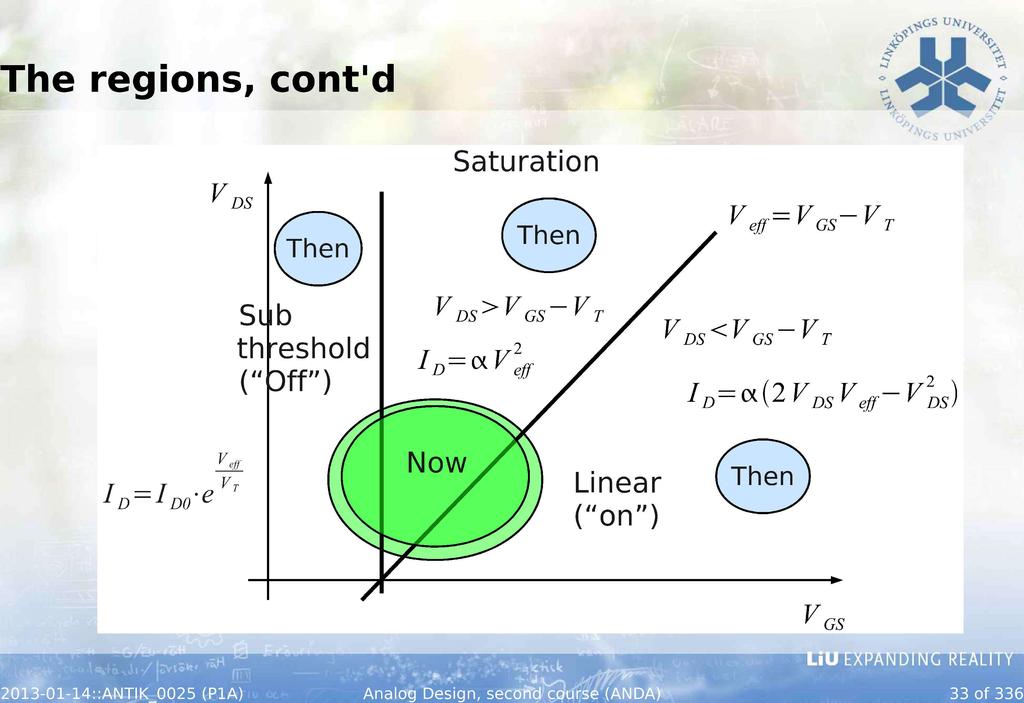
32 The regions Subthreshold (cut-off) Linear (low gain) Saturation (high gain) I 0 I α ( 2 V eff V ds V 2ds ) I α V 2eff V eff <0 V eff >0, V ds <V eff V eff >0, V ds >V eff 32 of 336
33
34 The second-order effects Subthreshold I I D0 e Linear V eff k T /q Saturation I α ( 2 V eff V ds V 2 ds ) V ds I α V 1+ Vθ 2 eff ( ) V T =V T0 +γ ( 2 Φ F V BS 2 Φ F ), V θ=1/ λ 34 of 336
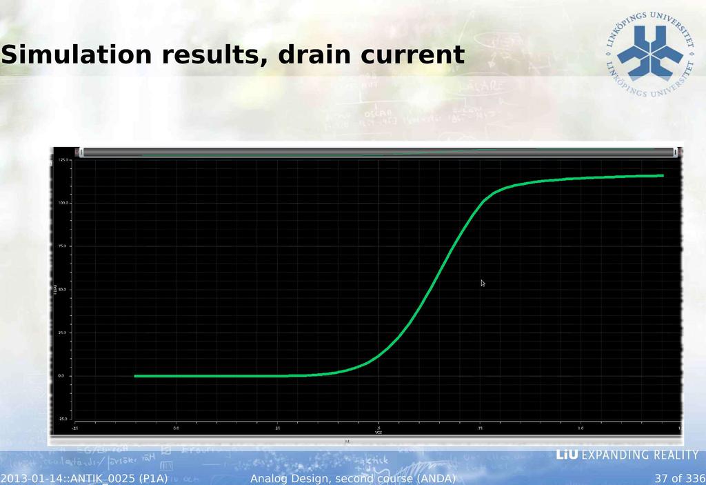
35 The first amplifier A common-source amplifier v out =V DD R L I D RL Saturation region V out v out =V DD R L α %v 2eff V in Linear region v out =V DD R L α ( 2 v out %v eff v 2 out ) M1 35 of 336
36 A simple testbench 36 of 336
37

38 The second order effects 38 of 336
 is the DC gain. The peak is reduced.")
39 The second-order effects, cont'd The derivative (lower graph) is the DC gain. The peak is reduced. 39 of 336

40 Board activities... The large-signal scenario Continued The small-signal scenario (Next lecture) Design centering Operating point 40 of 336
41 What did we do today? Introduction to the course Labs, quizzes, exam, etc. The transistor Operating regions Functionality First amplifier and parameters A starting point for the lessons 41 of 336

42 What will we do next time? Small-signal schematics Linearization Further work on the analog building blocks Common-source, common-drain, common-gate, etc. Stability and why 42 of 336
What will we do next time?
 What will we do next time? Amplifiers and differential pairs Why differential? Stability Why stability? Phase margin Compensation 62 of 113 Lecture 1, ANIK Introduction, CMOS Analog integrated circuits
Lecture 2, Amplifiers 1. Analog building blocks
 Lecture 2, Amplifiers 1 Analog building blocks Outline of today's lecture Further work on the analog building blocks Common-source, common-drain, common-gate Active vs passive load Other "simple" analog
Design cycle for MEMS
 Design cycle for MEMS Design cycle for ICs IC Process Selection nmos CMOS BiCMOS ECL for logic for I/O and driver circuit for critical high speed parts of the system The Real Estate of a Wafer MOS Transistor
EE 330 Laboratory 7 MOSFET Device Experimental Characterization and Basic Applications Spring 2017
 EE 330 Laboratory 7 MOSFET Device Experimental Characterization and Basic Applications Spring 2017 Objective: The objective of this laboratory experiment is to become more familiar with the operation of
ECE520 VLSI Design. Lecture 2: Basic MOS Physics. Payman Zarkesh-Ha
 ECE520 VLSI Design Lecture 2: Basic MOS Physics Payman Zarkesh-Ha Office: ECE Bldg. 230B Office hours: Wednesday 2:00-3:00PM or by appointment E-mail: pzarkesh@unm.edu Slide: 1 Review of Last Lecture Semiconductor
Introduction to VLSI ASIC Design and Technology
 Introduction to VLSI ASIC Design and Technology Paulo Moreira CERN - Geneva, Switzerland Paulo Moreira Introduction 1 Outline Introduction Is there a limit? Transistors CMOS building blocks Parasitics
Lecture 16: MOS Transistor models: Linear models, SPICE models. Context. In the last lecture, we discussed the MOS transistor, and
 Lecture 16: MOS Transistor models: Linear models, SPICE models Context In the last lecture, we discussed the MOS transistor, and added a correction due to the changing depletion region, called the body
MOS IC Amplifiers. Token Ring LAN JSSC 12/89
 MO IC Amplifiers MOFETs are inferior to BJTs for analog design in terms of quality per silicon area But MO is the technology of choice for digital applications Therefore, most analog portions of mixed-signal
EEC 118 Spring 2010 Lab #1: NMOS and PMOS Transistor Parameters
 EEC 118 Spring 2010 Lab #1: NMOS and PMOS Transistor Parameters Dept. of Electrical and Computer Engineering University of California, Davis March 18, 2010 Reading: Rabaey Chapter 3 [1]. Reference: Kang
ETIN25 Analogue IC Design. Laboratory Manual Lab 2
 Department of Electrical and Information Technology LTH ETIN25 Analogue IC Design Laboratory Manual Lab 2 Jonas Lindstrand Martin Liliebladh Markus Törmänen September 2011 Laboratory 2: Design and Simulation
DIGITAL VLSI LAB ASSIGNMENT 1
 DIGITAL VLSI LAB ASSIGNMENT 1 Problem 1: NMOS and PMOS plots using Cadence. In this exercise, you are required to generate both NMOS and PMOS I-V device characteristics (I/P and O/P) using Cadence (Use
Chapter 1. Introduction
 EECS3611 Analog Integrated Circuit esign Chapter 1 Introduction EECS3611 Analog Integrated Circuit esign Instructor: Prof. Ebrahim Ghafar-Zadeh, Prof. Peter Lian email: egz@cse.yorku.ca peterlian@cse.yorku.ca
Design and Layout of Two Stage High Bandwidth Operational Amplifier
 Design and Layout of Two Stage High Bandwidth Operational Amplifier Yasir Mahmood Qureshi Abstract This paper presents the design and layout of a two stage, high speed operational amplifiers using standard
Analysis and Design of Analog Integrated Circuits Lecture 8. Cascode Techniques
 Analysis and Design of Analog Integrated Circuits Lecture 8 Cascode Techniques Michael H. Perrott February 15, 2012 Copyright 2012 by Michael H. Perrott All rights reserved. Review of Large Signal Analysis
Chapter 2 : Semiconductor Materials & Devices (II) Feb
 Feb") Chapter 2 : Semiconductor Materials & Devices (II) 1 Reference 1. SemiconductorManufacturing Technology: Michael Quirk and Julian Serda (2001) 3. Microelectronic Circuits (5/e): Sedra & Smith (2004) 4.
Chapter 2 : Semiconductor Materials & Devices (II) 1 Reference 1. SemiconductorManufacturing Technology: Michael Quirk and Julian Serda (2001) 3. Microelectronic Circuits (5/e): Sedra & Smith (2004) 4.
ECEN474/704: (Analog) VLSI Circuit Design Fall 2016
 VLSI Circuit Design Fall 2016") ECEN474/704: (Analog) VLSI Circuit Design Fall 2016 Lecture 1: Introduction Sam Palermo Analog & Mixed-Signal Center Texas A&M University Announcements Turn in your 0.18um NDA form by Thursday Sep 1 No
ECEN474/704: (Analog) VLSI Circuit Design Fall 2016 Lecture 1: Introduction Sam Palermo Analog & Mixed-Signal Center Texas A&M University Announcements Turn in your 0.18um NDA form by Thursday Sep 1 No
Analog Integrated Circuit Design Exercise 1
 Analog Integrated Circuit Design Exercise 1 Integrated Electronic Systems Lab Prof. Dr.-Ing. Klaus Hofmann M.Sc. Katrin Hirmer, M.Sc. Sreekesh Lakshminarayanan Status: 21.10.2015 Pre-Assignments The lecture
ECEN 474/704 Lab 5: Frequency Response of Inverting Amplifiers
 ECEN 474/704 Lab 5: Frequency Response of Inverting Amplifiers Objective Design, simulate and layout various inverting amplifiers. Introduction Inverting amplifiers are fundamental building blocks of electronic
University of Pittsburgh
 University of Pittsburgh Experiment #4 Lab Report MOSFET Amplifiers and Current Mirrors Submission Date: 07/03/2018 Instructors: Dr. Ahmed Dallal Shangqian Gao Submitted By: Nick Haver & Alex Williams
Metal Oxide Semiconductor Field-Effect Transistors (MOSFETs)
") Metal Oxide Semiconductor Field-Effect Transistors (MOSFETs) Device Structure N-Channel MOSFET Providing electrons Pulling electrons (makes current flow) + + + Apply positive voltage to gate: Drives away
Metal Oxide Semiconductor Field-Effect Transistors (MOSFETs) Device Structure N-Channel MOSFET Providing electrons Pulling electrons (makes current flow) + + + Apply positive voltage to gate: Drives away
Chapter 4. CMOS Cascode Amplifiers. 4.1 Introduction. 4.2 CMOS Cascode Amplifiers
 Chapter 4 CMOS Cascode Amplifiers 4.1 Introduction A single stage CMOS amplifier cannot give desired dc voltage gain, output resistance and transconductance. The voltage gain can be made to attain higher
Lecture 26 - Design Problems & Wrap-Up. May 15, 2003
 6.012 Microelectronic Devices and Circuits - Spring 2003 Lecture 26-1 Lecture 26 - Design Problems & 6.012 Wrap-Up May 15, 2003 Contents: 1. Design process 2. Design project pitfalls 3. Lessons learned
8. Characteristics of Field Effect Transistor (MOSFET)
") 1 8. Characteristics of Field Effect Transistor (MOSFET) 8.1. Objectives The purpose of this experiment is to measure input and output characteristics of n-channel and p- channel field effect transistors
1 8. Characteristics of Field Effect Transistor (MOSFET) 8.1. Objectives The purpose of this experiment is to measure input and output characteristics of n-channel and p- channel field effect transistors
INF4420 Switched capacitor circuits Outline
 INF4420 Switched capacitor circuits Spring 2012 1 / 54 Outline Switched capacitor introduction MOSFET as an analog switch z-transform Switched capacitor integrators 2 / 54 Introduction Discrete time analog
Experiment #7 MOSFET Dynamic Circuits II
 Experiment #7 MOSFET Dynamic Circuits II Jonathan Roderick Introduction The previous experiment introduced the canonic cells for MOSFETs. The small signal model was presented and was used to discuss the
Carleton University. Faculty of Engineering and Design, Department of Electronics. ELEC 2507 Electronic - I Summer Term 2017
 Carleton University Faculty of Engineering and Design, Department of Electronics Instructors: ELEC 2507 Electronic - I Summer Term 2017 Name Section Office Email Prof. Q. J. Zhang Section A 4148 ME qjz@doe.carleton.ca
Analog IC Design 2010
 Analog IC Design 2010 Lecture 7 CAD tools, Simulation and layout Markus Törmänen Markus.Tormanen@eit.lth.se All images are taken from Gray, Hurst, Lewis, Meyer, 5th ed., unless noted otherwise. Contents
EE Analog and Non-linear Integrated Circuit Design
 University of Southern California Viterbi School of Engineering Ming Hsieh Department of Electrical Engineering EE 479 - Analog and Non-linear Integrated Circuit Design Instructor: Ali Zadeh Email: prof.zadeh@yahoo.com
Electronic Circuits for Mechatronics ELCT 609 Lecture 6: MOS-FET Transistor
 Electronic Circuits for Mechatronics ELCT 609 Lecture 6: MOS-FET Transistor Assistant Professor Office: C3.315 E-mail: eman.azab@guc.edu.eg 1 Introduction Why we call it Transistor? The name came as an
4.2.2 Metal Oxide Semiconductor Field Effect Transistor (MOSFET)
") 4.2.2 Metal Oxide Semiconductor Field Effect Transistor (MOSFET) The Metal Oxide Semitonductor Field Effect Transistor (MOSFET) has two modes of operation, the depletion mode, and the enhancement mode.
4.2.2 Metal Oxide Semiconductor Field Effect Transistor (MOSFET) The Metal Oxide Semitonductor Field Effect Transistor (MOSFET) has two modes of operation, the depletion mode, and the enhancement mode.
6.976 High Speed Communication Circuits and Systems Lecture 5 High Speed, Broadband Amplifiers
 6.976 High Speed Communication Circuits and Systems Lecture 5 High Speed, Broadband Amplifiers Michael Perrott Massachusetts Institute of Technology Copyright 2003 by Michael H. Perrott Broadband Communication
Submission date: Wednesday 21/3/2018
 Faculty of Information Engineering & Technology Electrical & Electronics Department Course: Microelectronics Lab ELCT605 Spring 2018 Dr. Eman Azab Eng. Samar Shukry Analog Report 1, 2 DC, TRANSIENT, AND
Lecture Wrap up. December 13, 2005
 6.012 Microelectronic Devices and Circuits Fall 2005 Lecture 26 1 Lecture 26 6.012 Wrap up December 13, 2005 Contents: 1. 6.012 wrap up Announcements: Final exam TA review session: December 16, 7:30 9:30
INF4420. Switched capacitor circuits. Spring Jørgen Andreas Michaelsen
 INF4420 Switched capacitor circuits Spring 2012 Jørgen Andreas Michaelsen (jorgenam@ifi.uio.no) Outline Switched capacitor introduction MOSFET as an analog switch z-transform Switched capacitor integrators
Communication Microelectronics ELCT508 (W17) Lecture 1: Introduction Dr. Eman Azab Assistant Professor Office: C
 Lecture 1: Introduction Dr. Eman Azab Assistant Professor Office: C") Communication Microelectronics ELCT508 (W17) Lecture 1: Introduction Assistant Professor Office: C3.315 E-mail: eman.azab@guc.edu.eg 1 Course Team Lecturer Teaching Assistants Contact Information E-mail:
Communication Microelectronics ELCT508 (W17) Lecture 1: Introduction Assistant Professor Office: C3.315 E-mail: eman.azab@guc.edu.eg 1 Course Team Lecturer Teaching Assistants Contact Information E-mail:
CMOS Technology for Computer Architects
 CMOS Technology for Computer Architects Lecture 1: Introduction Iakovos Mavroidis Giorgos Passas Manolis Katevenis FORTH-ICS (University of Crete) Course Contents Implementation of high-performance digital
MOS Field-Effect Transistors (MOSFETs)
") 6 MOS Field-Effect Transistors (MOSFETs) A three-terminal device that uses the voltages of the two terminals to control the current flowing in the third terminal. The basis for amplifier design. The basis
6 MOS Field-Effect Transistors (MOSFETs) A three-terminal device that uses the voltages of the two terminals to control the current flowing in the third terminal. The basis for amplifier design. The basis
Electronic Circuits for Mechatronics ELCT609 Lecture 1: Introduction
 Electronic Circuits for Mechatronics ELCT609 Lecture 1: Introduction Assistant Professor Office: C3.315 E-mail: eman.azab@guc.edu.eg 1 Course Team Contact Information Lecturer Teaching Assistants E-mail:
Lecture 34: Designing amplifiers, biasing, frequency response. Context
 Lecture 34: Designing amplifiers, biasing, frequency response Prof J. S. Smith Context We will figure out more of the design parameters for the amplifier we looked at in the last lecture, and then we will
Physics 364, Fall 2012, reading due your answers to by 11pm on Thursday
 Physics 364, Fall 2012, reading due 2012-10-25. Email your answers to ashmansk@hep.upenn.edu by 11pm on Thursday Course materials and schedule are at http://positron.hep.upenn.edu/p364 Assignment: (a)
Microelectronics Exercises of Topic 5 ICT Systems Engineering EPSEM - UPC
 Microelectronics Exercises of Topic 5 ICT Systems Engineering EPSEM - UPC F. Xavier Moncunill Autumn 2018 5 Analog integrated circuits Exercise 5.1 This problem aims to follow the steps in the design of
Analysis and Design of Analog Integrated Circuits Lecture 20. Advanced Opamp Topologies (Part II)
") Analysis and Design of Analog Integrated Circuits Lecture 20 Advanced Opamp Topologies (Part II) Michael H. Perrott April 15, 2012 Copyright 2012 by Michael H. Perrott All rights reserved. Outline of Lecture
Analysis and Design of Analog Integrated Circuits Lecture 20 Advanced Opamp Topologies (Part II) Michael H. Perrott April 15, 2012 Copyright 2012 by Michael H. Perrott All rights reserved. Outline of Lecture
MOS Capacitance and Introduction to MOSFETs
 ECE-305: Fall 2016 MOS Capacitance and Introduction to MOSFETs Professor Peter Bermel Electrical and Computer Engineering Purdue University, West Lafayette, IN USA pbermel@purdue.edu 11/4/2016 Pierret,
An Improved Bandgap Reference (BGR) Circuit with Constant Voltage and Current Outputs
 Circuit with Constant Voltage and Current Outputs") International Journal of Research in Engineering and Innovation Vol-1, Issue-6 (2017), 60-64 International Journal of Research in Engineering and Innovation (IJREI) journal home page: http://www.ijrei.com
International Journal of Research in Engineering and Innovation Vol-1, Issue-6 (2017), 60-64 International Journal of Research in Engineering and Innovation (IJREI) journal home page: http://www.ijrei.com
d. Can you find intrinsic gain more easily by examining the equation for current? Explain.
 EECS140 Final Spring 2017 Name SID 1. [8] In a vacuum tube, the plate (or anode) current is a function of the plate voltage (output) and the grid voltage (input). I P = k(v P + µv G ) 3/2 where µ is a
Analog IC Design. Lecture 1,2: Introduction & MOS transistors. Henrik Sjöland. Dept. of Electrical and Information Technology
 Analog IC Design Lecture 1,2: Introduction & MOS transistors Henrik.Sjoland@eit.lth.se Part 1: Introduction Analogue IC Design (7.5hp, lp2) CMOS Technology Analog building blocks in CMOS Single- and multiple
An Analog Phase-Locked Loop
 1 An Analog Phase-Locked Loop Greg Flewelling ABSTRACT This report discusses the design, simulation, and layout of an Analog Phase-Locked Loop (APLL). The circuit consists of five major parts: A differential
Lecture 0: Introduction
 Lecture 0: Introduction Introduction Integrated circuits: many transistors on one chip. Very Large Scale Integration (VLSI): bucketloads! Complementary Metal Oxide Semiconductor Fast, cheap, low power
EE105 Fall 2015 Microelectronic Devices and Circuits: MOSFET Prof. Ming C. Wu 511 Sutardja Dai Hall (SDH)
") EE105 Fall 2015 Microelectronic Devices and Circuits: MOSFET Prof. Ming C. Wu wu@eecs.berkeley.edu 511 Sutardja Dai Hall (SDH) 7-1 Simplest Model of MOSFET (from EE16B) 7-2 CMOS Inverter 7-3 CMOS NAND
EE105 Fall 2015 Microelectronic Devices and Circuits: MOSFET Prof. Ming C. Wu wu@eecs.berkeley.edu 511 Sutardja Dai Hall (SDH) 7-1 Simplest Model of MOSFET (from EE16B) 7-2 CMOS Inverter 7-3 CMOS NAND
Low voltage, low power, bulk-driven amplifier
 University of Arkansas, Fayetteville ScholarWorks@UARK Electrical Engineering Undergraduate Honors Theses Electrical Engineering 5-2009 Low voltage, low power, bulk-driven amplifier Shama Huda University
INF4420. Outline. Switched capacitor circuits. Switched capacitor introduction. MOSFET as an analog switch 1 / 26 2 / 26.
 INF4420 Switched capacitor circuits Spring 2012 Jørgen Andreas Michaelsen (jorgenam@ifi.uil.no) 1 / 26 Outline Switched capacitor introduction MOSFET as an analog switch 2 / 26 Introduction Discrete time
EE 320 L LABORATORY 9: MOSFET TRANSISTOR CHARACTERIZATIONS. by Ming Zhu UNIVERSITY OF NEVADA, LAS VEGAS 1. OBJECTIVE 2. COMPONENTS & EQUIPMENT
 EE 320 L ELECTRONICS I LABORATORY 9: MOSFET TRANSISTOR CHARACTERIZATIONS by Ming Zhu DEPARTMENT OF ELECTRICAL AND COMPUTER ENGINEERING UNIVERSITY OF NEVADA, LAS VEGAS 1. OBJECTIVE Get familiar with MOSFETs,
EE4800 CMOS Digital IC Design & Analysis. Lecture 1 Introduction Zhuo Feng
 EE4800 CMOS Digital IC Design & Analysis Lecture 1 Introduction Zhuo Feng 1.1 Prof. Zhuo Feng Office: EERC 730 Phone: 487-3116 Email: zhuofeng@mtu.edu Class Website http://www.ece.mtu.edu/~zhuofeng/ee4800fall2010.html
Course Outcome of M.Tech (VLSI Design)
") Course Outcome of M.Tech (VLSI Design) PVL108: Device Physics and Technology The students are able to: 1. Understand the basic physics of semiconductor devices and the basics theory of PN junction. 2.
Course Outcome of M.Tech (VLSI Design) PVL108: Device Physics and Technology The students are able to: 1. Understand the basic physics of semiconductor devices and the basics theory of PN junction. 2.
Session 2 MOS Transistor for RF Circuits
 Session 2 MOS Transistor for RF Circuits Session Speaker Chandramohan P. Session Contents MOS transistor basics MOS equivalent circuit Single stage amplifiers Opamp design Session objectives To understand
ET475 Electronic Circuit Design I [Onsite]
![ET475 Electronic Circuit Design I [Onsite]](/thumbs/89/98281525.jpg "ET475 Electronic Circuit Design I [Onsite]") ET475 Electronic Circuit Design I [Onsite] Course Description: This course covers the analysis and design of electronic circuits, and includes a laboratory that utilizes computer-aided software tools for
ET475 Electronic Circuit Design I [Onsite] Course Description: This course covers the analysis and design of electronic circuits, and includes a laboratory that utilizes computer-aided software tools for
What is the typical voltage gain of the basic two stage CMOS opamp we studied? (i) 20dB (ii) 40dB (iii) 80dB (iv) 100dB
 20dB (ii) 40dB (iii) 80dB (iv) 100dB") Department of Electronic ELEC 5808 (ELG 6388) Signal Processing Electronics Final Examination Dec 14th, 2010 5:30PM - 7:30PM R. Mason answer all questions one 8.5 x 11 crib sheets allowed 1. (5 points)
Department of Electronic ELEC 5808 (ELG 6388) Signal Processing Electronics Final Examination Dec 14th, 2010 5:30PM - 7:30PM R. Mason answer all questions one 8.5 x 11 crib sheets allowed 1. (5 points)
CS/EE 181a 2010/11 Lecture 1
 CS/EE 181a 2010/11 Lecture 1 CS/EE 181 is about designing digital CMOS systems. Functional Specification Approximate domain of CS181 Circuit Specification Simulation Architectural Specification Abstract
6.776 High Speed Communication Circuits Lecture 6 MOS Transistors, Passive Components, Gain- Bandwidth Issue for Broadband Amplifiers
 6.776 High Speed Communication Circuits Lecture 6 MOS Transistors, Passive Components, Gain- Bandwidth Issue for Broadband Amplifiers Massachusetts Institute of Technology February 17, 2005 Copyright 2005
Field Effect Transistors
 Field Effect Transistors Purpose In this experiment we introduce field effect transistors (FETs). We will measure the output characteristics of a FET, and then construct a common-source amplifier stage,
Basic Circuits. Current Mirror, Gain stage, Source Follower, Cascode, Differential Pair,
 Basic Circuits Current Mirror, Gain stage, Source Follower, Cascode, Differential Pair, CCS - Basic Circuits P. Fischer, ZITI, Uni Heidelberg, Seite 1 Reminder: Effect of Transistor Sizes Very crude classification:
0.85V. 2. vs. I W / L
 EE501 Lab3 Exploring Transistor Characteristics and Design Common-Source Amplifiers Lab report due on September 22, 2016 Objectives: 1. Be familiar with characteristics of MOSFET such as gain, speed, power,
Design of a Restartable Clock Generator for Use in GALS SoCs
 Design of a Restartable Clock Generator for Use in GALS SoCs Masters Thesis Defense Hu Wang August 6, 2008 IC Design and Research Laboratory Design Team Southern Illinois University Edwardsville Dr. George
Advanced Operational Amplifiers
 IsLab Analog Integrated Circuit Design OPA2-47 Advanced Operational Amplifiers כ Kyungpook National University IsLab Analog Integrated Circuit Design OPA2-1 Advanced Current Mirrors and Opamps Two-stage
Integrated Circuit Amplifiers. Comparison of MOSFETs and BJTs
 Integrated Circuit Amplifiers Comparison of MOSFETs and BJTs 17 Typical CMOS Device Parameters 0.8 µm 0.25 µm 0.13 µm Parameter NMOS PMOS NMOS PMOS NMOS PMOS t ox (nm) 15 15 6 6 2.7 2.7 C ox (ff/µm 2 )
Homework Assignment 07
 Homework Assignment 07 Question 1 (Short Takes). 2 points each unless otherwise noted. 1. A single-pole op-amp has an open-loop low-frequency gain of A = 10 5 and an open loop, 3-dB frequency of 4 Hz.
Depletion-mode operation ( 공핍형 ): Using an input gate voltage to effectively decrease the channel size of an FET
: Using an input gate voltage to effectively decrease the channel size of an FET") Ch. 13 MOSFET Metal-Oxide-Semiconductor Field-Effect Transistor : I D D-mode E-mode V g The gate oxide is made of dielectric SiO 2 with e = 3.9 Depletion-mode operation ( 공핍형 ): Using an input gate voltage
Ch. 13 MOSFET Metal-Oxide-Semiconductor Field-Effect Transistor : I D D-mode E-mode V g The gate oxide is made of dielectric SiO 2 with e = 3.9 Depletion-mode operation ( 공핍형 ): Using an input gate voltage
Digital Electronics. Assign 1 and 0 to a range of voltage (or current), with a separation that minimizes a transition region. Positive Logic.
, with a separation that minimizes a transition region. Positive Logic.") Digital Electronics Assign 1 and 0 to a range of voltage (or current), with a separation that minimizes a transition region Positive Logic Logic 1 Negative Logic Logic 0 Voltage Transition Region Transition
Digital Electronics Assign 1 and 0 to a range of voltage (or current), with a separation that minimizes a transition region Positive Logic Logic 1 Negative Logic Logic 0 Voltage Transition Region Transition
Academic Course Description. VL2004 CMOS Analog VLSI Second Semester, (Even semester)
") Academic Course Description SRM University Faculty of Engineering and Technology Department of Electronics and Communication Engineering VL2004 CMOS Analog VLSI Second Semester, 2013-14 (Even semester)
Academic Course Description SRM University Faculty of Engineering and Technology Department of Electronics and Communication Engineering VL2004 CMOS Analog VLSI Second Semester, 2013-14 (Even semester)
EECS150 - Digital Design Lecture 2 - CMOS
 EECS150 - Digital Design Lecture 2 - CMOS August 29, 2002 John Wawrzynek Fall 2002 EECS150 - Lec02-CMOS Page 1 Outline Overview of Physical Implementations CMOS devices Announcements/Break CMOS transistor
INTRODUCTION TO ELECTRONICS EHB 222E
 INTRODUCTION TO ELECTRONICS EHB 222E MOS Field Effect Transistors (MOSFETS II) MOSFETS 1/ INTRODUCTION TO ELECTRONICS 1 MOSFETS Amplifiers Cut off when v GS < V t v DS decreases starting point A, once
Design and Simulation of Low Dropout Regulator
 Design and Simulation of Low Dropout Regulator Chaitra S Kumar 1, K Sujatha 2 1 MTech Student, Department of Electronics, BMSCE, Bangalore, India 2 Assistant Professor, Department of Electronics, BMSCE,
2009 Spring CS211 Digital Systems & Lab 1 CHAPTER 3: TECHNOLOGY (PART 2)
") 1 CHAPTER 3: IMPLEMENTATION TECHNOLOGY (PART 2) Whatwillwelearninthischapter? we learn in this 2 How transistors operate and form simple switches CMOS logic gates IC technology FPGAs and other PLDs Basic
1 CHAPTER 3: IMPLEMENTATION TECHNOLOGY (PART 2) Whatwillwelearninthischapter? we learn in this 2 How transistors operate and form simple switches CMOS logic gates IC technology FPGAs and other PLDs Basic
Device Technologies. Yau - 1
 Device Technologies Yau - 1 Objectives After studying the material in this chapter, you will be able to: 1. Identify differences between analog and digital devices and passive and active components. Explain
NAME: Last First Signature
 UNIVERSITY OF CALIFORNIA, BERKELEY College of Engineering Department of Electrical Engineering and Computer Sciences EE 130: IC Devices Spring 2003 FINAL EXAMINATION NAME: Last First Signature STUDENT
Yet, many signal processing systems require both digital and analog circuits. To enable
 Introduction Field-Programmable Gate Arrays (FPGAs) have been a superb solution for rapid and reliable prototyping of digital logic systems at low cost for more than twenty years. Yet, many signal processing
ECE 255, MOSFET Amplifiers
 ECE 255, MOSFET Amplifiers 26 October 2017 In this lecture, the basic configurations of MOSFET amplifiers will be studied similar to that of BJT. Previously, it has been shown that with the transistor
ECE315 / ECE515 Lecture 7 Date:
 Lecture 7 ate: 01.09.2016 CG Amplifier Examples Biasing in MOS Amplifier Circuits Common Gate (CG) Amplifier CG Amplifier- nput is applied at the Source and the output is sensed at the rain. The Gate terminal
Lecture 20 Transistor Amplifiers (II) Other Amplifier Stages
 Other Amplifier Stages") Lecture 20 Transistor Amplifiers (II) Other Amplifier Stages Outline Common drain amplifier Common gate amplifier Reading Assignment: Howe and Sodini; Chapter 8, Sections 8.78.9 6.02 Spring 2009 . Common
Lecture 20 Transistor Amplifiers (II) Other Amplifier Stages Outline Common drain amplifier Common gate amplifier Reading Assignment: Howe and Sodini; Chapter 8, Sections 8.78.9 6.02 Spring 2009 . Common
Review Sheet for Midterm #2
 Review Sheet for Midterm #2 Brian Bircumshaw brianb@eecs.berkeley.edu 1 Miterm #1 Review See Table 1 on the following page for a list of the most important equations you should know from Midterm #1. 2
DAT175: Topics in Electronic System Design
 DAT175: Topics in Electronic System Design Analog Readout Circuitry for Hearing Aid in STM90nm 21 February 2010 Remzi Yagiz Mungan v1.10 1. Introduction In this project, the aim is to design an adjustable
Design of Gain Enhanced and Power Efficient Op- Amp for ADC/DAC and Medical Applications
 Indian Journal of Science and Technology, Vol 9(29), DOI: 10.17485/ijst/2016/v9i29/90885, August 2016 ISSN (Print) : 0974-6846 ISSN (Online) : 0974-5645 Design of Gain Enhanced and Power Efficient Op-
Reading. Lecture 17: MOS transistors digital. Context. Digital techniques:
 Reading Lecture 17: MOS transistors digital Today we are going to look at the analog characteristics of simple digital devices, 5. 5.4 And following the midterm, we will cover PN diodes again in forward
Electronic Circuits. Junction Field-effect Transistors. Dr. Manar Mohaisen Office: F208 Department of EECE
 Electronic Circuits Junction Field-effect Transistors Dr. Manar Mohaisen Office: F208 Email: manar.subhi@kut.ac.kr Department of EECE Review of the Precedent Lecture Explain the Operation Class A Power
ELEC 350L Electronics I Laboratory Fall 2012
 ELEC 350L Electronics I Laboratory Fall 2012 Lab #9: NMOS and CMOS Inverter Circuits Introduction The inverter, or NOT gate, is the fundamental building block of most digital devices. The circuits used
Device Technology( Part 2 ): CMOS IC Technologies
: CMOS IC Technologies") 1 Device Technology( Part 2 ): CMOS IC Technologies Chapter 3 : Semiconductor Manufacturing Technology by M. Quirk & J. Serda Saroj Kumar Patra, Department of Electronics and Telecommunication, Norwegian
1 Device Technology( Part 2 ): CMOS IC Technologies Chapter 3 : Semiconductor Manufacturing Technology by M. Quirk & J. Serda Saroj Kumar Patra, Department of Electronics and Telecommunication, Norwegian
Design of Rail-to-Rail Op-Amp in 90nm Technology
 IJSTE - International Journal of Science Technology & Engineering Volume 1 Issue 2 August 2014 ISSN(online) : 2349-784X Design of Rail-to-Rail Op-Amp in 90nm Technology P R Pournima M.Tech Electronics
Low-Voltage Wide Linear Range Tunable Operational Transconductance Amplifier
 Low-Voltage Wide Linear Range Tunable Operational Transconductance Amplifier A dissertation submitted in partial fulfillment of the requirement for the award of degree of Master of Technology in VLSI Design
Experiment #6 MOSFET Dynamic circuits
 Experiment #6 MOSFET Dynamic circuits Jonathan Roderick Introduction: This experiment will build upon the concepts that were presented in the previous lab and introduce dynamic circuits using MOSFETS.
ECE315 / ECE515 Lecture 9 Date:
 Lecture 9 Date: 03.09.2015 Biasing in MOS Amplifier Circuits Biasing using Single Power Supply The general form of a single-supply MOSFET amplifier biasing circuit is: We typically attempt to satisfy three
Common-Source Amplifiers
 Lab 2: Common-Source Amplifiers Introduction The common-source stage is the most basic amplifier stage encountered in CMOS analog circuits. Because of its very high input impedance, moderate-to-high gain,
Microelectronic Circuits II. Ch 10 : Operational-Amplifier Circuits
 Microelectronic Circuits II Ch 0 : Operational-Amplifier Circuits 0. The Two-stage CMOS Op Amp 0.2 The Folded-Cascode CMOS Op Amp CNU EE 0.- Operational-Amplifier Introduction - Analog ICs : operational
Radivoje Đurić, 2015, Analogna Integrisana Kola 1
 OTA-output buffer 1 According to the types of loads, the driving capability of the output stages differs. For switched capacitor circuits which have high impedance capacitive loads, class A output stage
A new class AB folded-cascode operational amplifier
 A new class AB folded-cascode operational amplifier Mohammad Yavari a) Integrated Circuits Design Laboratory, Department of Electrical Engineering, Amirkabir University of Technology, Tehran, Iran a) myavari@aut.ac.ir
1 FUNDAMENTAL CONCEPTS What is Noise Coupling 1
 Contents 1 FUNDAMENTAL CONCEPTS 1 1.1 What is Noise Coupling 1 1.2 Resistance 3 1.2.1 Resistivity and Resistance 3 1.2.2 Wire Resistance 4 1.2.3 Sheet Resistance 5 1.2.4 Skin Effect 6 1.2.5 Resistance
BJT Amplifier. Superposition principle (linear amplifier)
") BJT Amplifier Two types analysis DC analysis Applied DC voltage source AC analysis Time varying signal source Superposition principle (linear amplifier) The response of a linear amplifier circuit excited
BJT Amplifier Two types analysis DC analysis Applied DC voltage source AC analysis Time varying signal source Superposition principle (linear amplifier) The response of a linear amplifier circuit excited
ENEE307 Lab 7 MOS Transistors 2: Small Signal Amplifiers and Digital Circuits
 ENEE307 Lab 7 MOS Transistors 2: Small Signal Amplifiers and Digital Circuits In this lab, we will be looking at ac signals with MOSFET circuits and digital electronics. The experiments will be performed
ECEN474: (Analog) VLSI Circuit Design Fall 2011
 VLSI Circuit Design Fall 2011") ECEN474: (Analog) VLSI Circuit Design Fall 2011 Lecture 1: Introduction Sebastian Hoyos Analog & Mixed-Signal Center Texas A&M University Analog Circuit Sequence 326 2 Why is Analog Important? [Silva]
ECEN474: (Analog) VLSI Circuit Design Fall 2011 Lecture 1: Introduction Sebastian Hoyos Analog & Mixed-Signal Center Texas A&M University Analog Circuit Sequence 326 2 Why is Analog Important? [Silva]
Designing of a 8-bits DAC in 0.35µm CMOS Technology For High Speed Communication Systems Application
 Designing of a 8-bits DAC in 035µm CMOS Technology For High Speed Communication Systems Application Veronica Ernita Kristianti, Hamzah Afandi, Eri Prasetyo ibowo, Brahmantyo Heruseto and shinta Kisriani
Digital Electronics Part II - Circuits
 Digital Electronics Part II - Circuits Dr. I. J. Wassell Gates from Transistors 1 Introduction Logic circuits are non-linear, consequently we will introduce a graphical technique for analysing such circuits