P21XXCSR-EVB P21XXPowerharvester Chipset Reference Design Evaluation Board
|
|
|
- Felix Gray
- 6 years ago
- Views:
Transcription
1 DESCRIPTION The P21XXCSR-EB is an evaluation board featuring PCC110 and PCC210 chips with support for six frequency bandsto test and develop with the Powerharvester Chipset Reference Design. The P21XXCSR converts radio frequency (RF) energy into DC power and stores it in a capacitor to provide an intermittent, regulated voltage output. Frequency bands supported: GSM-850 uplink Europe RFID & GSM-850 downlink ISM USA & GSM-900 uplink GSM-1800 uplink GSM-1900 uplink WiFi 2.4GHz ORDERING INFORMATION The P21XXCSR can be evaluated on the P21XXCSR-EB evaluation board. Contact Powercast for information about obtaining one of the reference designs on the P21XXCSR-EB for integration onto your PCB. The chipset is listed under part numbers PCC110 & PCC210. Additional CSR designs are available to support different frequencies and power ranges. Send requests to: contact@powercastco.com. ITEMS INCLUDED 1 for Powerharvester Chipset Reference Designs Notes 1. This kit requires a user provided antenna. Contact Powercast for custom antenna designs: contact@powercastco.com. 2. This kit needs to receive power from an RF source with sufficient transmit power. Test equipment can be used to testany band. A DC blockmust be added if the antenna or test equipment is a DC short. Other common sources include: Powercast TX901 Transmitter RFID readers Cell phones WiFi routers INSTRUCTIONS 1. Connect an antenna to the SMA connector (J1 J6) on the evaluation board, or connect J1 J6 directly to RF test equipment. Exceeding the ratings may cause permanent damage. 2. Select the corresponding band(s) using JP2. 3. Adjust switches S2, S3, and S4 to the desired settings. See the descriptions on the next page. 4. Place the evaluation board on a flat surface and connect test meters as desired. 5. Turn on the source of RF energy (e.g. Powercaster transmitter, test equipment, other transmitter) P a g e 1

 sensitive device.")
2 P21XXCSR-EBEALUATION BOARD ABSOLUTE MAXIMUM RATINGS T A = 25 C, unless otherwise noted. Parameter Rating Unit RF Input Power 23 RF IN to GND 0 D SET to GND 6 RESET to GND 6 CAP to GND 2.3 OUT to GND 6 OUT Current 100 ma Operating Temperature Range -40 to 85 C Storage Temperature Range -40 to 140 C Exceeding the absolute maximum ratings may cause permanent damage to the device. ESD CAUTION This is an ESD (electrostatic discharge) sensitive device. Proper ESD precautions should be taken to avoid degradation or damage to the component. P a g e 2
3 COMPONENT DESCRIPTION Component BT1, BT2 C1 C2 C3 C4, Q5, Q6, R17, R18 D3 J1 J2 J3 J4 J5 J6 JP1 JP2 P1 Description External battery connection (described in detail below) Storage capacitor 2200μF (small) Storage capacitor not populated (user determined) Storage capacitor 50mF (large) Output switch (described in detail below) LED for visual indication of power output SMA connector for antenna or RF input at MHz (add DC block for DC short antenna) SMA connector for antenna or RF input at MHz (add DC block for DC short antenna) SMA connector for antenna or RF input at 904 MHz (add DC block for DC short antenna) SMA connector for antenna or RF input at MHz (add DC block for DC short antenna) SMA connector for antenna or RF input at 1880 MHz (add DC block for DC short antenna) SMA connector for antenna or RF input at 2450 MHz (add DC block for DC short antenna) Jumper for selecting storage capacitor C1, C2, or C3 Jumper for selecting desired band(s) of RF input Connector for add-on boards Connector on board: Sullins P/N: SBH11-PBPC-D05-ST-BK Mating connector: Sullins P/N: SFH11-PBPC-D05-ST-BK JP3, JP4, JP5 Jumpers for selecting threshold voltage of boost converter R1, R2 Resistors for setting OUT default value (changing these resistors will change the voltage setpoints of switch S1) R3, R4 Resistors for adjusting OUT, selectable using S1 R5 R6 R7 S1 S2 S3 LED bias resistor Resistor for pulling D SET high using OUT, selectable using S2 Resistor for limiting current to low impedance batteries Switch for selecting output voltage (described in detail below) Switch for D SET selection (described in detail below) Switch for selecting OUT load (described in detail below) P a g e 3
4 SPECIFICATIONS T A = 25 C, OUT = 3.3, RF IN = 0,unless otherwise noted. Parameter Symbol Condition Min Typ Max Unit RF Characteristics 1 Input Power (836.5 MHz) Input Power (879.5 MHz) Input Power (904 MHz) Input Power ( MHz) Input Power (1880 MHz) Input Power (2450 MHz) DC Characteristics Output oltage Output Current CAPMaximum (1.2 setting) CAPMinimum (1.2 setting) CAPMaximum (0.9 setting) CAPMinimum (0.9 setting) CAPMaximum (0.7 setting) CAPMinimum (0.7 setting) Boost Efficiency Maximum INT Current Digital Characteristics RESET Input High DSETInput High INT Output High Timing Characteristics DSETDelay RESET Delay RESET Pulse Width 1.2 INT & OUT On-time 0.9 INT & OUTOn-time 0.7 INT & OUTOn-time OUT IOUT MAX MIN MAX MIN 2 MAX MIN 2 IOUT= 20mA MIN MAX ma % ma μs μs ns ms ms ms 1 See typical performance graphs for operation at other frequencies or power levels. Minimum value is dependent on the JP3, JP4, or JP5 selection. 2 Based on the on-board RC values 3 Approximately equal to MAX for 0.9 and 0.7 settings 4 Into on-board LED P a g e 4
5 TIMING DIAGRAM DETAILED COMPONENT DESCRIPTIONS AND OPERATING INSTRUCTIONS Selecting RF Band JP2 is used to select the desired band(s) of RF signal to be harvested by the system. There are six different bands, each with a corresponding SMA connector for attaching an antenna (J1-J6). Component Band Band (MHz) Center Frequency (MHz) J1 GSM-850 uplink J2 Europe RFID & GSM-850 downlink J3 ISM USA & GSM-900 uplink J4 GSM-1800 uplink J5 GSM-1900 uplink J6 WiFi 2.4GHz Selecting Storage Capacitor JP1 is used to select the storage capacitor used in the system. C1 is a 2200uF electrolytic capacitor. C2 is left unpopulated but is a universal footprint so that a user can add a different capacitor to the board. C3 is a 50mF super capacitor with low ESR. P a g e 5
6 Typical Operation The harvester circuit converts RF energy within the appropriate frequency band into DC power. This is monitored by one of three voltage detectors. The user selects 1.2, 0.9 or 0.7 as the threshold voltage via JP3, JP4 or JP5 respectively. The storage capacitor, selected via JP1, then charges up to the selected threshold voltage. When CAPreachesits maximum value (MAX), INT is set high, the boost converter turns on, and OUTis set to the output voltage selected via S1.The storage capacitor then discharges until CAPreaches its minimum value (MIN) and then sets INT low, shutting off the boost converter until CAP charges back up to its maximum value. RSSI Operation (D OUT, D SET ) The RSSI functionality allows the sampling of the received signal to provide an indication of the amount of energy being harvested. When D SET is driven high the harvested DC power will be directed to a resistor, and the corresponding voltage will be provided to D OUT. The voltage on D OUT can be read after a 50μs settling time. When the RSSI functionality is being used, the harvested DC power is not being stored.if the RSSI functionality is not used, D OUT and D SET should be left unconnected. D SET has an onboard pull down. Reset (RESET) The RESET function allows the voltage from OUT to be turned off before the storage capacitor reaches the lower threshold, MIN, thereby saving energy and improving the recharge time back to the activation threshold, MAX. The RESET function can be implemented by a microcontroller. When the function of the microcontroller is completed, driving RESET high will disable the voltage from OUT. Care should be taken to ensure that the microcontroller, especially during power-on, does not inadvertently drive RESET high. This will immediately shutdown the output voltage.if the RESET functionality is not used, RESET should be left unconnected. Interrupt (INT) The interrupt function provides a digital indication that voltage is present at the OUT pin. INT can be used in more sophisticated systems that contain other storage elements and can be used as an external interrupt to bring a device such as microcontroller out of a deep sleep mode. The digital high level of the INT pin will be between MIN and MAX. The INT pin can provide a maximum of 0.1mA of current.if the INT functionality is not used, INT should be left unconnected. Selecting Turn-On oltage JP3, JP4 and JP5 are used to select the capacitor voltage at which the boost converter will turn on. Each is a four pin header, and the two two-pin jumpers are moved to the header corresponding to the desired threshold voltage. JP3 sets the threshold to 1.2, JP4 sets the threshold to 0.9, and JP5 sets the threshold to 0.7. P a g e 6
7 Selecting/Setting Output oltage S1 is used to select between three output voltage options for OUT. Selecting DEFAULT sets OUT to 3.3. Selecting 4.1 or 4.2 changes OUT to the labeled voltage. The DEFAULT setting can also be adjusted to any voltage between 2.0 and 5.5 simply by changing the resistors R1 and R2 and using the DEFAULT switch position. The equation for determining R1 and R2 is as follows: R2 = R1 ( OUT ) Itis recommended that a 1MΩ be used for R1, which is connected between OUTand SET. With this in mind, some common values for OUT would result in the following R2 values: For OUT = 3.3, R2 = 578.9kΩ (576kΩ std) For OUT = 4.1, R2 = 418.7kΩ (417kΩ std) For OUT = 4.2, R2 = 404.7kΩ (407kΩ std) It should be noted that changing R1 or R2 will change the voltage set by switch S1. Care should be taken to ensure the absolute maximum voltage is not exceeded. Selecting DSET S2 is used to select how DSET and DOUT function on the board. Selecting OFF will allow the P21XXCSR- EB to operate normally. If it is desired to monitor DOUT, selecting OUT will tie DSET to OUT through a resistor, R6. In this mode, when OUT is on, DSET will be pulled high and DOUT can be used to measure RSSI or to retrieve data from the RF field. Selecting DSET EXT will allow DSET to be controlled externally using the DSET EXT test point. LED, Prototyping, and Measuring Current S3 is used to control flow of current from OUT. Selecting LED will tie OUT to the on-board LED, D3, to be a visual indicator that the system working. Selecting CC will tie OUT to the prototype area and output switch. NOTE: OUT is routed to the header P1 in parallel with S3, so OUT is present on the header pins regardless of S3 position. If using the P1 header, S3 should be in the MEAS position, as the other positions could use more power, resulting in longer charging periods on the storage cap. Selecting MEAS allows for current to be measure by connected a current probe between test points OUT and LED or OUT and CC. Current should be measured using an oscilloscope, as the time period of OUTbeing on is generally too short to be seen on a multi-meter. Output Switch and Batteries With S3 in the CC position, the output switch is activated. The output switch includes C4, Q5, Q6, R17 and R18, and is necessary when using the P21XXCSR-EB to charge a battery. The switch limits the current draw on the battery from the P21XXCSR-EB to 10-20nA. This ensures the P21XXCSR-EB does not discharge the battery during periods of non-harvesting. P a g e 7
8 BT1 is a connection point used for charging a high impedance storage element (cell resistance >25 ohms) such as thin-film batteries or supercapacitors. The cell impedance of these types of batteries will limit the current drawn from the P21XXCSR-EB. BT2 is a connection point used for charging a low impedance battery such as Li-ion or Alkaline rechargeable. Resistor R7 is in series with this connection to limit current flow between the output switch and the battery. P a g e 8


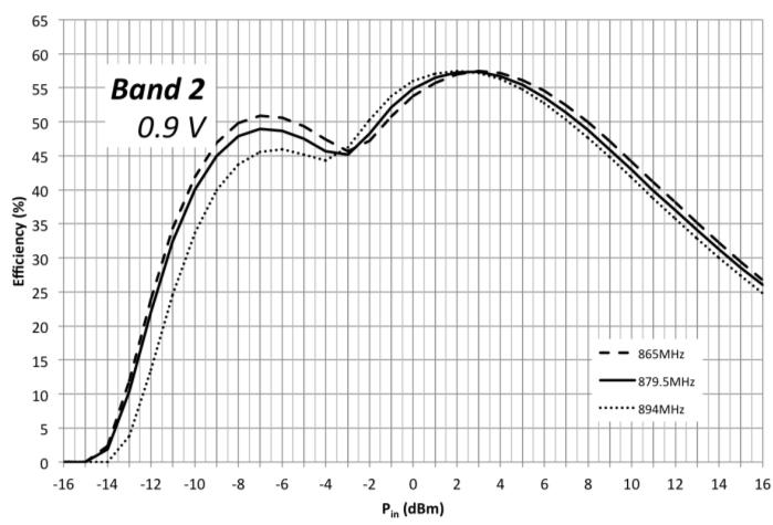
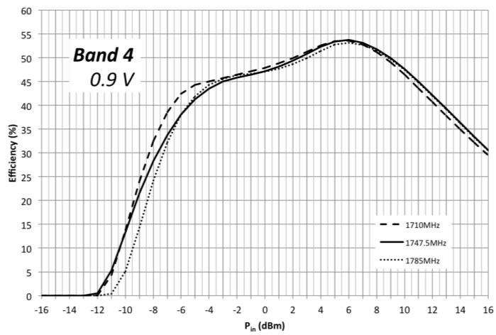
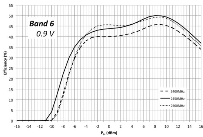
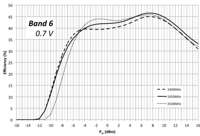
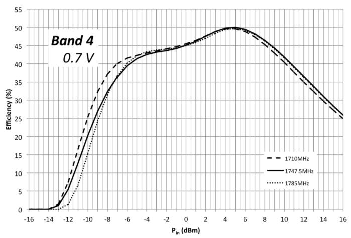
9 TYPICAL PERFORMANCE GRAPHS TA = 25 C, No jumper on JP2, Keithley 2400 Sourcemeter as load,unless otherwise noted Powerharvester Efficiency vs. RF IN () P a g e 9

10 P a g e 10

11 P a g e 11
P2110B 915 MHz RF Powerharvester Receiver
 DESCRIPTION The Powercast Powerharvester is an RF energy harvesting device that converts RF to DC. Housed in a compact SMD package, the receiver provides RF energy harvesting and power management for battery-free,
Product Datasheet P MHz RF Powerharvester Receiver
 GND GND GND NC NC NC Product Datasheet DESCRIPTION The Powercast P2110 Powerharvester receiver is an RF energy harvesting device that converts RF to DC. Housed in a compact SMD package, the P2110 receiver
LED level meter driver, 12-point, linear scale, dot or bar display
 LED level meter driver, 12-point, linear scale, dot or bar display The is a monolithic IC for LED level meter applications. The display level range is 0mVrms to 300mVrms (typ.) divided into 12 equally-spaced
EVALUATION KIT MANUAL FOLLOWS DATA SHEET Step-Up DC-DC Converters with Precise, Adaptive Current Limit for GSM PART* MAX1687EUE MAX1687ESA MAX1688EUE
 19-1426; Rev 0; 2/99 EALUATI KIT MANUAL FOLLOWS DATA SHEET Step-Up DC-DC Converters with General Description The / step-up DC-DC converters deliver up to 2W from a single Li-Ion or three NiMH cells. The
SGM mA Buck/Boost Charge Pump LED Driver
 GENERAL DESCRIPTION The SGM3140 is a current-regulated charge pump ideal for powering high brightness LEDs for camera flash applications. The charge pump can be set to regulate two current levels for FLASH
CMD170P GHz Driver Amplifier. Features. Functional Block Diagram. Description
 Features Functional Block Diagram High output power On-chip detector All positive bias Pb-free RoHs compliant 4x4 QFN package Description The CMD170P4 is a GaAs MMIC driver amplifier housed in a leadless
AEM Evaluation board for AEM Features. Description. Applications. Device information. Appearance. User guide
 Evaluation board for Description The evaluation board is a printed circuit board (PCB) featuring all the needed components to operate the integrated circuit (IC). Please refer to the datasheet for all
SGM mA Buck/Boost Charge Pump LED Driver
 GENERAL DESCRIPTION The SGM3140 is a current-regulated charge pump ideal for powering high brightness LEDs for camera flash applications. The charge pump can be set to regulate two current levels for Flash
Extending Cell Phone Battery Life with the ISL9109
 Extending Cell Phone Battery Life with the ISL9109 Application Note AN1424.0 In this day and age practically everyone is armed with a cell phone. Some of these smart phones not only work as a cell phone
LVDS Flow Through Evaluation Boards. LVDS47/48EVK Revision 1.0
 LVDS Flow Through Evaluation Boards LVDS47/48EVK Revision 1.0 January 2000 6.0.0 LVDS Flow Through Evaluation Boards 6.1.0 The Flow Through LVDS Evaluation Board The Flow Through LVDS Evaluation Board
±50V Isolated, 3.0V to 5.5V, 250kbps, 2 Tx/2 Rx, RS-232 Transceiver MAX3250
 EVALUATION KIT AVAILABLE MAX325 General Description The MAX325 is a 3.V to 5.5V powered, ±5V isolated EIA/TIA-232 and V.28/V.24 communications interface with high data-rate capabilities. The MAX325 is
SGM % Efficient Synchronous Step-Up Converter with 1A Switch
 Preliminary Datasheet SGM0 GERAL DESCRIPTION The SGM0 is a constant frequency, current mode, synchronous, step-up switching regulator. Its output currents can go as high as 7mA while using a single-cell
Figure 1 Typical Application Circuit. Figure 2 Application Circuit for Less Than 4 LEDs
 FOUR CHANNEL CONSTANT CURRENT LED DRIVER June 2014 GENERAL DESCRIPTION The IS31BL3212 provides four regulated current sources, delivers up to 23mA of load current to accommodate four white LEDs. It requires
RT9187C. 600mA, Ultra-Low Dropout, CMOS Regulator. General Description. Features. Applications. Ordering Information. Pin Configurations (TOP VIEW)
") 600mA, Ultra-Low Dropout, CMOS Regulator General Description The is a high-performance, 600mA LDO regulator, offering extremely high PSRR and ultra-low dropout. This chip is ideal for portable RF and wireless
600mA, Ultra-Low Dropout, CMOS Regulator General Description The is a high-performance, 600mA LDO regulator, offering extremely high PSRR and ultra-low dropout. This chip is ideal for portable RF and wireless
SGM3122 White LED Charge Pump Current Source with PWM Brightness Control
 GENERAL DESCRIPTION The SGM3122 is a charge pump with PWM brightness control for white LED supplies in LCD display backlight applications. The supply voltage ranges from 2.7V to 5.5V, it is ideally suited
HMC601LP4 / 601LP4E POWER DETECTORS - SMT. 75 db, FAST SETTLING, LOGARITHMIC DETECTOR / CONTROLLER MHz. Typical Applications.
 v.9 HMC6LP4 / 6LP4E 7 db, FAST SETTLING, LOGARITHMIC DETECTOR / CONTROLLER - 4 MHz Typical Applications The HMC6LP4(E) is ideal for IF and RF applications in: Cellular/PCS/G WiMAX, WiBro & Fixed Wireless
±15kV ESD-Protected, 3.0V to 5.5V, Low-Power, up to 250kbps, True RS-232 Transceiver
 19-1949; Rev ; 1/1 ±15k ESD-Protected, 3. to 5.5, Low-Power, General Description The is a 3-powered EIA/TIA-232 and.28/.24 communications interface with low power requirements, high data-rate capabilities,
SYN501R Datasheet. ( MHz Low Voltage ASK Receiver) Version 1.0
 Version 1.0") SYN501R Datasheet (300-450MHz Low Voltage ASK Receiver) Version 1.0 Contents 1. General Description... 1 2. Features... 1 3. Applications... 1 4. Typical Application... 2 5. Pin Configuration... 2 6. Pin
SYN501R Datasheet (300-450MHz Low Voltage ASK Receiver) Version 1.0 Contents 1. General Description... 1 2. Features... 1 3. Applications... 1 4. Typical Application... 2 5. Pin Configuration... 2 6. Pin
RS232-B1 User Manual V1.2 05/10/2017
 RS232-B1 User Manual V1.2 05/10/2017 Table of Contents 1. Introduction...2 1.1 Device Overview... 2 1.2 System Overview... 3 1.3 Features... 3 1.4 Connectors... 4 1.4.1 RS232 Connectors (J1, J2)... 4 1.4.2
VLA Hybrid Gate Driver Application Information. DC-DC Converter V D 15V. V iso = 2500V RMS
 Application NOTES: Last Revision November 15, 2004 VLA500-01 Hybrid Gate Driver Application Information Contents: 1. General Description 2. Short Circuit Protection 2.1 Destaruation Detection 2.2 VLA500-01
Lifetime Power Energy Harvesting Development Kit for Wireless Sensors User s Manual - featuring PIC MCU with extreme Low Power (XLP) Technology
 Technology") P2110-EVAL-01 Lifetime Power User s Manual - featuring PIC MCU with extreme Low Power (XLP) Technology Overview The Lifetime Power is a complete demonstration and development platform for creating battery-free
P2110-EVAL-01 Lifetime Power User s Manual - featuring PIC MCU with extreme Low Power (XLP) Technology Overview The Lifetime Power is a complete demonstration and development platform for creating battery-free
HMC600LP4 / 600LP4E POWER DETECTORS - SMT. 75 db LOGARITHMIC DETECTOR / CONTROLLER MHz. Features. Typical Applications. General Description
 v.99 HMC6LP4 / 6LP4E 7 db LOGARITHMIC DETECTOR / CONTROLLER - 4 MHz Typical Applications The HMC6LP4 / HMC6LP4E is ideal for IF and RF applications in: Cellular/PCS/G WiMAX, WiBro & Fixed Wireless Power
1-24 GHz Distributed Driver Amplifier
 Features Functional Block Diagram Wide bandwidth High linearity Single positive supply voltage On chip bias choke Description The CMD197C4 is a wideband GaAs MMIC driver amplifier housed in a leadless
SYN500R Datasheet. ( MHz ASK Receiver) Version 1.0
 Version 1.0") SYN500R Datasheet (300-450MHz ASK Receiver) Version 1.0 Contents 1. General Description... 1 2. Features... 1 3. Applications... 1 4. Typical Application... 2 5. Pin Configuration... 2 6. Pin Description...
SYN500R Datasheet (300-450MHz ASK Receiver) Version 1.0 Contents 1. General Description... 1 2. Features... 1 3. Applications... 1 4. Typical Application... 2 5. Pin Configuration... 2 6. Pin Description...
5- to 10-Cell Li+ Protector with Cell Balancing
 Rev 0; 4/08 5- to 10-Cell Li+ Protector with Cell Balancing General Description The provides full charge and discharge protection for 5- to 10-cell lithium-ion (Li+) battery packs. The protection circuit
v02.06 Insertion Loss INSERTION LOSS () C +85 C -40 C Isolation ISOLATION () Return Loss RETURN LOSS ()
 C +85 C -40 C Isolation ISOLATION () Return Loss RETURN LOSS ()") v02.06 Typical Applications The is ideal for: Telecom Infrastructure Microwave Radio & VSAT Military Radios, Radar & ECM Space Systems Test Instrumentation Features Isolation: 55 @ 2 GHz 42 @ 6 GHz Insertion
v02.06 Typical Applications The is ideal for: Telecom Infrastructure Microwave Radio & VSAT Military Radios, Radar & ECM Space Systems Test Instrumentation Features Isolation: 55 @ 2 GHz 42 @ 6 GHz Insertion
Product Specification PE42850
 Product Description The PE4850 is a HaRP technology-enhanced SP5T high power RF switch supporting wireless applications up to GHz. It offers maximum power handling of 4.5 m continuous wave (CW). It delivers
OBSOLETE. 9 khz. Operation Frequency 9 khz. db 6000 MHz. db Return Loss RF1, RF2 and RFC
 Product Description The PE455 RF Switch is designed to support the requirements of the test equipment and ATE market. This broadband general purpose switch maintains excellent RF performance and linearity
RT9187B. 600mA, Ultra-Low Dropout, Ultra-Fast CMOS LDO Regulator. General Description. Features. Applications. Ordering Information RT9187B
 6mA, Ultra-Low Dropout, Ultra-Fast CMOS LDO Regulator General Description The is a high-performance, 6mA LDO regulator, offering extremely high PSRR and ultra-low dropout. This chip is ideal for portable
QLG1 GPS Receiver kit
 QLG1 GPS Receiver kit 1. Introduction Thank you for purchasing the QRP Labs QLG1 GPS Receiver kit. This kit will provide a highly sensitive, highly accurate GPS receiver module, using the popular MediaTek
Low Noise 300mA LDO Regulator General Description. Features
 Low Noise 300mA LDO Regulator General Description The id9301 is a 300mA with fixed output voltage options ranging from 1.5V, low dropout and low noise linear regulator with high ripple rejection ratio
IS31BL3228A/B WHITE LED DRIVER. January 2016
 WHITE LED DRIVER January 2016 GENERAL DESCRIPTION The IS31BL3228A (IS31BL3228B) is a low noise, constant frequency charge pump DC/DC converter for white LED applications. The IS31BL3228A (IS31BL3228B)
SGM2576/SGM2576B Power Distribution Switches
 /B GENERAL DESCRIPTION The and B are integrated typically 100mΩ power switch for self-powered and bus-powered Universal Series Bus (USB) applications. The and B integrate programmable current limiting
Dual-Output Step-Down and LCD Step-Up Power Supply for PDAs
 19-2248; Rev 2; 5/11 EVALUATI KIT AVAILABLE Dual-Output Step-Down and LCD Step-Up General Description The dual power supply contains a step-down and step-up DC-DC converter in a small 12-pin TQFN package
LSP2031 is a dual input, 3A ultra low dropout linear regulator. To achieve an extremely low dropout voltage,
 General Description LSP2031 is a dual input, 3A ultra low dropout linear regulator. To achieve an extremely low dropout voltage, LSP2031 has a control voltage input for the circuitry and a main supply
MADR V to 250V Driver for High Power PIN Diode Switches Rev. V1. Functional Schematic. Features. Description. Pin Configuration 1
 Features 20 V to 250 V Back Bias in Off State 200 ma Series Diode Bias Current at +25 C 50 ma Shunt Diode Bias Current at +25 C Propagation Delay less than 8 µs Low Quiescent Current Consumption 3 V or
DEMO MANUAL DC2473A LTC6419 Dual Differential Amplifier/ADC Driver DESCRIPTION
 DESCRIPTION Demonstration circuit 7A features the LTC 9 Dual Differential Amplifier/ADC Driver. It incorporates a variety of passive components to support configurations for varied applications. These
CY520 Datasheet. 300M-450MHz ASK Receiver. General Description. Features. Applications CY520
 CY520 Datasheet 300M-450MHz ASK Receiver General Description The CY520 is a general purpose, 3.3-5V ASK Receiver that operates from 300M to 450MHz with typical sensitivity of -109dBm. The CY520 functions
RT2517B. 1A, 6V, Ultra-Low Dropout Linear Regulator. General Description. Features. Applications. Ordering Information. Marking Information
 RT2517B 1A, 6V, Ultra-Low Dropout Linear Regulator General Description The RT2517B is a high performance positive voltage regulator designed for use in applications requiring ultralow input voltage and
RF4432 wireless transceiver module
 1. Description www.nicerf.com RF4432 RF4432 wireless transceiver module RF4432 adopts Silicon Lab Si4432 RF chip, which is a highly integrated wireless ISM band transceiver. The features of high sensitivity
Advanced Monolithic Systems
 Advanced Monolithic Systems FEATURES Internal Power Switch Output Voltage up to 20V Up to 89% Efficiency Low 0.08µA Shutdown Supply Current Internal Current Limit Thermal Shutdown Available in 5-Pin SOT-23
Product Specification PE45450
 PE45450 Product Description The PE45450 is a HaRP technology-enhanced power limiter designed for use in high performance power limiting applications in test and measurement equipment, radar, military electronic
1 MHz to 10 GHz, 45 db Log Detector/Controller AD8319
 FEATURES Wide bandwidth: 1 MHz to 10 GHz High accuracy: ±1.0 db over temperature 45 db dynamic range up to 8 GHz Stability over temperature: ±0.5 db Low noise measurement/controller output VOUT Pulse response
SKY : Direct Quadrature Demodulator GHz Featuring No-Pull LO Architecture
 PRELIMINARY DATA SHEET SKY73013-306: Direct Quadrature Demodulator 4.9 5.925 GHz Featuring No-Pull LO Architecture Applications WiMAX, WLAN receivers UNII Band OFDM receivers RFID, DSRC applications Proprietary
CSI021 4 Channel High Voltage Programmable Current Sink/Source
 CSI021 4 Channel High Voltage Programmable Current Sink/Source CSI021 NeuroStim ASSP Datasheet Rev 1.3 FEATURES 4 Output Channels per IC Independent 8 Bit DAC Programmability SPI Programmable Output Current
Features MIC1555 VS MIC1557 VS OUT 5
 MIC555/557 MIC555/557 IttyBitty RC Timer / Oscillator General Description The MIC555 IttyBitty CMOS RC timer/oscillator and MIC557 IttyBitty CMOS RC oscillator are designed to provide rail-to-rail pulses
Ultralow Power Voltage Comparator with Reference ADCMP380
 Data Sheet Ultralow Power Voltage Comparator with Reference FEATURES Comparator with on-chip reference Ultralow power consumption with ICC = 92 na (typical) Precision low voltage monitoring down to.5 V
Features. FREQUENCY 900MHz 1950MHz 2450MHz NF (db) NF (db) IIP3 (dbm) GAIN (db)
 NF (db) IIP3 (dbm) GAIN (db)") EVALUATION KIT AVAILABLE MAX// to.ghz, Low-Noise, General Description The MAX// miniature, low-cost, low-noise downconverter mixers are designed for lowvoltage operation and are ideal for use in portable
EVALUATION KIT AVAILABLE MAX// to.ghz, Low-Noise, General Description The MAX// miniature, low-cost, low-noise downconverter mixers are designed for lowvoltage operation and are ideal for use in portable
Features SLEW ENA ELA VDD. 332k ELB RSW MIC M COM REL ENB GND. VIN Li Ion 3V to 4.2V 2.2nF 250V. Low Noise Dual EL Driver
 Low Noise Dual 22 V PP Driver With Output Voltage Slew Rate Control General Description The is a low noise dual Electroluminescent () Panel driver used in backlighting applications. The converts a low
DESCRIPTION FEATURES APPLICATIONS TYPICAL APPLICATION. 500KHz, 18V, 2A Synchronous Step-Down Converter
 DESCRIPTION The is a fully integrated, high-efficiency 2A synchronous rectified step-down converter. The operates at high efficiency over a wide output current load range. This device offers two operation
Features. Applications
 105MHz Low-Power SOT23-5 Op Amp General Description The is a high-speed operational amplifier which is unity gain stable regardless of resistive and capacitive load. It provides a gain-bandwidth product
Features db
 v1.19 DETECTOR / CONTROLLER, 5-8 MHz Power Detectors - SMT Typical Applications The is ideal for: Cellular Infrastructure WiMAX, WiBro & LTE/G Power Monitoring & Control Circuitry Receiver Signal Strength
Parameters Symbol Min. Typ. Max. Unit Condition Frequency Range. Frequency Stability and Aging ppm ppm ppm ppm
 Features Frequencies between 115.194001 MHz to 137 MHz accurate to 6 decimal places Operating temperature from -40 C to +125 C. For -55 C option, refer to MO8920 and MO8921 Supply voltage of +1.8V or +2.5V
DC to 1000 MHz IF Gain Block ADL5530
 DC to MHz IF Gain Block ADL3 FEATURES Fixed gain of 6. db Operation up to MHz 37 dbm Output Third-Order Intercept (OIP3) 3 db noise figure Input/output internally matched to Ω Stable temperature and power
Passive High-Function RFID: Sensors and Bi-Stable Displays
 Passive High-Function RFID: Sensors and Bi-Stable Displays May 4, 2015 Charles Greene, Ph.D. Chief Technical Officer EDN 2010 Hot 100 Emerging Technology P2100 Powerharvester TX91501 Powercaster P2110
Value Units -0.3 to +4.0 V -50 to
 Designed for Short-Range Wireless Data Communications Supports 2.4-19.2 kbps Encoded Data Transmissions 3 V, Low Current Operation plus Sleep Mode Ready to Use OEM Module The DR3100 transceiver module
USB-B1 User Manual V1.1
 USB-B1 User Manual V1.1 Table of Contents 1 Introduction... 2 1.1 Device Overview... 2 1.2 System Overview... 3 1.3 Connectors... 4 1.3.1 USB Connector J11... 4 1.3.2 External Antenna Connector (J10)...
SGM6132 3A, 28.5V, 1.4MHz Step-Down Converter
 GENERAL DESCRIPTION The SGM6132 is a current-mode step-down regulator with an internal power MOSFET. This device achieves 3A continuous output current over a wide input supply range from 4.5V to 28.5V
SGM6130 3A, 28.5V, 385kHz Step-Down Converter
 GENERAL DESCRIPTION The SGM6130 is a current-mode step-down regulator with an internal power MOSFET. This device achieves 3A continuous output current over a wide input supply range from 4.5 to 28.5 with
LN2402. PWM/PFM Automatic Switching Controlled Synchronous DC-DC Converters. General Description. Applications. Package. Features
 PWM/PFM Automatic Switching Controlled Synchronous DC-DC Converters General Description The is a constant frequency, current mode step-down converter. It is ideal for powering portable equipment that runs
MIC94040/1/2/3. Features. General Description. Applications. Typical Application. 28mΩ R DSON 3A High Side Load Switch in 1.2mm x 1.
 28mΩ R DSON 3A High Side Load Switch in 1.2mm x 1.2mm MLF package General Description The is a family of high-side load switches designed to operate from 1.7V to 5.5V input voltage. The load switch pass
CY803/802 Datasheet. 300M-450MHz RF receiver CY803/802/802R. General Description. Features. Ordering Information. Typical Application
 CY803/802 Datasheet 300M-450MHz RF receiver General Description The CY803/802 is a general purpose, 3.3-5V, super-heterodyne Receiver that operates from 300M to 450MHz with typical sensitivity of -110dBm.
DNT24MCA DNT24MPA. Low Cost 2.4 GHz FHSS Transceiver Modules with I/O. DNT24MCA/MPA Absolute Maximum Ratings. DNT24MCA/MPA Electrical Characteristics
 - 2.4 GHz Frequency Hopping Spread Spectrum Transceivers - Direct Peer-to-peer Low Latency Communication - Transmitter RF Power Configurable - 10 or 63 mw - Built-in Chip Antenna - 250 kbps RF Data Rate
DEMO MANUAL DC1646A LTC GHz RF Power Detector with Comparator Description
 LTC556 15GHz RF Power Detector with Comparator Description The demonstration circuit 166A features the LTC 556, an UltraFast RF peak detector with a built in gain-selectable high speed operational amplifier
Product Specification PE42920
 PE42920 Product Description The PE42920 is a dual differential single pole double throw (DDSPDT) RF switch developed on Peregrine s UltraCMOS process technology. It is a broadband and low loss device enabling
Extremely Accurate Power Surveillance, Software Monitoring and Sleep Mode Detection. Pin Assignment. Fig. 1
 EM MICOELECTONIC - MAIN SA Extremely Accurate Power Surveillance, Software Monitoring and Sleep Mode Detection Description The offers a high level of integration by voltage monitoring and software monitoring
Standalone Linear Li-Ion Battery Charger with Thermal Regulation
 Standalone Linear Li-Ion Battery Charger with Thermal Regulation FEATURES DESCRIPTION Programmable Charge Current up to 1A No MOSFET, Sense Resistor or Blocking Diode Required Constant-Current/Constant-Voltage
HM2259D. 2A, 4.5V-20V Input,1MHz Synchronous Step-Down Converter. General Description. Features. Applications. Package. Typical Application Circuit
 HM2259D 2A, 4.5V-20V Input,1MHz Synchronous Step-Down Converter General Description Features HM2259D is a fully integrated, high efficiency 2A synchronous rectified step-down converter. The HM2259D operates
SKY : 5 GHz Low-Noise Amplifier
 DATA SHEET SKY6544-31: 5 GHz Low-Noise Amplifier Applications _ENABLE CC 82.11a/n/ac radios 5 GHz ISM radios Smartphones Bias Notebooks, netbooks, and tablets Access points, routers, and gateways RF_IN
MP3115 High-Efficiency, Single-Cell Alkaline, 1.3MHz Synchronous Step-up Converter with Output Disconnect
 The Future of Analog IC Technology MP3115 High-Efficiency, Single-Cell Alkaline, 1.3MHz Synchronous Step-up Converter with Output Disconnect DESCRIPTION The MP3115 is a synchronous, fixed frequency, current
Parameters Symbol Min. Typ. Max. Unit Condition Frequency Range Output Frequency Range f MHz
 Features Any frequency between 1 MHz and 110 MHz accurate to 6 decimal places Operating temperature from -40 C to +85 C. Refer to MO2018 for -40 C to +85 C option and MO2020 for -55 C to +125 C option
Features. = +25 C, With 0/-5V Control, 50 Ohm System. Parameter Frequency Min. Typ. Max. Units
 v03.15 Typical Applications The is ideal for: Telecom Infrastructure Microwave Radio & VSAT Military Radios, Radar & ECM Test Instrumentation Features Isolation: 55 @ 2 GHz 43 @ 6 GHz Insertion Loss: 1.6
HMC959LC3 HIGH SPEED LOGIC - SMT. 26 GHz, DIVIDE-BY-4 WITH RESET & PROGRAMMABLE OUTPUT VOLTAGE. Typical Applications. Features. Functional Diagram
 HMC959LC Typical Applications Features The HMC959LC is ideal for: High Speed Frequency Divider (up to 26 GHz) Broadband Test & Measurement Clock Synthesis Phase Locked Loops Functional Diagram Electrical
CONDOR C1722 GPS RECEIVER MODULE technical notes
 CONDOR C1722 GPS RECEIVER MODULE TECHNICAL HIGHLIGHTS Receiver: GPS L1 frequency (1575.42 MHz), C/A code, 22-channel continuous tracking NMEA output and input: serial port, USB port On-board low noise
FAN5602 Universal (Step-Up/Step-Down) Charge Pump Regulated DC/DC Converter
 Charge Pump Regulated DC/DC Converter") August 2009 FAN5602 Universal (Step-Up/Step-Down) Charge Pump Regulated DC/DC Converter Features Low-Noise, Constant-Frequency Operation at Heavy Load High-Efficiency, Pulse-Skip (PFM) Operation at Light
August 2009 FAN5602 Universal (Step-Up/Step-Down) Charge Pump Regulated DC/DC Converter Features Low-Noise, Constant-Frequency Operation at Heavy Load High-Efficiency, Pulse-Skip (PFM) Operation at Light
Low Cost Instrumentation Amplifier AD622
 a FEATURES Easy to Use Low Cost Solution Higher Performance than Two or Three Op Amp Design Unity Gain with No External Resistor Optional Gains with One External Resistor (Gain Range 2 to ) Wide Power
Features. = +25 C, With 0/-5V Control, 50 Ohm System. Parameter Frequency Min. Typ. Max. Units
 Typical Applications The is ideal for: Telecom Infrastructure Microwave Radio & VSAT Military Radios, Radar & ECM Space Systems Test Instrumentation Features Isolation: 48 @ 2 GHz 34 @ 6 GHz Insertion
Low Noise, DC/DC Charge Pump Regulator
 Low Noise, DC/DC Charge Pump Regulator Description The is a low noise DC/DC charge pump regulator that produces a regulated output voltage from 2.7V to 4.5V input voltage. Low external parts count (one
OUTPUT UP TO 300mA C2 TOP VIEW FAULT- DETECT OUTPUT. Maxim Integrated Products 1
 19-1422; Rev 2; 1/1 Low-Dropout, 3mA General Description The MAX886 low-noise, low-dropout linear regulator operates from a 2.5 to 6.5 input and is guaranteed to deliver 3mA. Typical output noise for this
±15kV ESD-Protected, 460kbps, 1µA, RS-232-Compatible Transceivers in µmax
 19-191; Rev ; 1/1 ±15kV ESD-Protected, 6kbps, 1µA, General Description The are low-power, 5V EIA/TIA- 3-compatible transceivers. All transmitter outputs and receiver inputs are protected to ±15kV using
MACP Temperature Compensated Directional RMS Power Detector 2-6 GHz Rev. V1 Features Integrated Directional Coupler Low Insertion Loss: 0.15 db
 Features Integrated Directional Coupler Low Insertion Loss: 0.15 db @ 4 GHz Min. detectable power: -15 dbm @ 4 GHz Dynamic range: 45 db @ 4 GHz Built-In Temperature Compensation Lead-Free 1.5 x 1.2 mm
PE4257. Product Specification. Product Description
 Product Description The PE is a high-isolation UltraCMOS Switch designed for wireless applications, covering a broad frequency range from near DC up to 000 MHz. This single-supply SPDT switch integrates
High Speed, G = +2, Low Cost, Triple Op Amp ADA4862-3
 High Speed,, Low Cost, Triple Op Amp ADA4862-3 FEATURES Ideal for RGB/HD/SD video Supports 8i/72p resolution High speed 3 db bandwidth: 3 MHz Slew rate: 75 V/μs Settling time: 9 ns (.5%). db flatness:
A mA STANDALONE LINEAR Li-ion BATTERY CHARGER THERMAL REGULATION
 DESCRIPTION The is a complete constant current / constant voltage linear charger for single cell Lithium-Ion batteries. No external sense resistor is needed, and no blocking diode is required due to the
PART TEMP RANGE PIN-PACKAGE
 General Description The MAX6922/MAX6932/ multi-output, 76V, vacuum-fluorescent display (VFD) tube drivers that interface a VFD tube to a microcontroller or a VFD controller, such as the MAX6850 MAX6853.
EEPROM-Programmable TFT VCOM Calibrator
 19-2911 Rev 3; 8/6 EVALUATION KIT AVAILABLE EEPROM-Programmable TFT Calibrator General Description The is a programmable -adjustment solution for thin-film transistor (TFT) liquid-crystal displays (LCDs).
HMC602LP4 / 602LP4E POWER DETECTORS - SMT. 70 db, LOGARITHMIC DETECTOR / CONTROLLER, MHz
 v3.9 HMC6LP / 6LPE 7 db, LOGARITHMIC DETECTOR / CONTROLLER, 1-8 MHz 1 Typical Applications The HMC6LP(E) is ideal for IF and RF applications in: Cellular/PCS/3G WiMAX, WiBro, WLAN, Fixed Wireless & Radar
HMC940LC4B. 13 Gbps, 1:4 FANOUT BUFFER w/ PROGRAMMABLE OUTPUT VOLTAGE. Typical Applications. Features. Functional Diagram. General Description
 Typical Applications Features The is ideal for: RF ATE Applications Broadband Test & Measurement Serial Data Transmission up to 13 Gbps Clock Buffering up to 13 GHz Functional Diagram Inputs Terminated
PIN CONFIGURATION FEATURES APPLICATIONS BLOCK DIAGRAM. D, F, N Packages
 DESCRIPTION Both the and - Dual Monolithic timing circuits are highly stable controllers capable of producing accurate time delays or oscillation. The and - are a dual. Timing is provided by an external
AMS2115 FAST TRANSIENT RESPONSE LDO CONTROLLER
 FAST TRANSIENT RESPONSE LDO CONTROLLER General Description The AMS5 is a single IC controller that drives an external N Channel MOSFET as a source follower to produce a fast transient response, low dropout
Parameter Min Typ Max Units Frequency Range
 Features Functional Block Diagram Low loss broadband performance High isolation Non-reflective design Integrated 3:8 TTL decoder Pb-free RoHs compliant 4x4 SMT package Description The CMD236C4 is a broadband
±15kV ESD-Protected, 1Mbps, 1µA RS-232 Transmitters in SOT23-6
 19-164; Rev 1; 3/ ±15k ESD-Protected, bps, 1 General Description The / single RS-3 transmitters in a SOT3-6 package are for space- and cost-constrained applications requiring minimal RS-3 communications.
Preliminary Datasheet
 Product Description Figure 2. Package Type The is a digitally controlled variable gain amplifier (DVGA) is featuring high linearity using the voltage 3V supply with a broadband frequency range of 30 to
PART TOP VIEW. OUT 3.3V AT 100mA POK. Maxim Integrated Products 1
 9-600; Rev ; 6/00 General Description The is a buck/boost regulating charge pump that generates a regulated output voltage from a single lithium-ion (Li+) cell, or two or three NiMH or alkaline cells for
2A,4.5V-21V Input,500kHz Synchronous Step-Down Converter FEATURES GENERAL DESCRIPTION APPLICATIONS TYPICAL APPLICATION
 2A,4.5-21 Input,500kHz Synchronous Step-Down Converter FEATURES High Efficiency: Up to 96% 500KHz Frequency Operation 2A Output Current No Schottky Diode Required 4.5 to 21 Input oltage Range 0.8 Reference
Dual-/Triple-/Quad-Voltage, Capacitor- Adjustable, Sequencing/Supervisory Circuits
 19-0525; Rev 3; 1/07 EVALUATION KIT AVAILABLE Dual-/Triple-/Quad-Voltage, Capacitor- General Description The are dual-/triple-/quad-voltage monitors and sequencers that are offered in a small TQFN package.
Product Specification PE42851
 PE42851 Product Description The PE42851 is a HaRP technology-enhanced SP5T high power RF switch supporting wireless applications up to 1 GHz. It offers maximum power handling of 42.5 m continuous wave
Features. OUT Intercept dbm Variation of OUT with Temperature from -40 C to dbm Input
 v.1 DETECTOR / CONTROLLER, 5-7 MHz Typical Applications The HMC713MS8(E) is ideal for: Cellular Infrastructure WiMAX, WiBro & LTE/G Power Monitoring & Control Circuitry Receiver Signal Strength Indication
DIO6305 High-Efficiency 1.2MHz, 1.1A Synchronous Step-Up Converter
 High-Efficiency 1.2MHz, 1.1A Synchronous Step-Up Converter Rev 1.2 Features High-Efficiency Synchronous-Mode 2.7-5.25V input voltage range Device Quiescent Current: 30µA (TYP) Less than 1µA Shutdown Current
MIC4414/4415. General Description. Features. Applications. Typical Application. 1.5A, 4.5V to 18V, Low-Side MOSFET Driver
 MIC4414/4415 1.5A, 4.5V to 18V, Low-Side MOSFET Driver General Description The MIC4414 and MIC4415 are low-side MOSFET drivers designed to switch an N-channel enhancement type MOSFET in low-side switch