Electronic Instrumentation. Experiment 8: Diodes (continued) Project 4: Optical Communications Link
|
|
|
- Lee Christian Sanders
- 6 years ago
- Views:
Transcription
1 Electronic Instrumentation Experiment 8: Diodes (continued) Project 4: Optical Communications Link
2 Agenda Brief Review: Diodes Zener Diodes Project 4: Optical Communication Link Why optics? Understanding Modulation Initial Design of optical link Transmitter Receiver PSpice Model Your final design
3 What you will know Half wave and full wave rectifier circuit Voltage limiter circuit What a Zener diode is used for How a signal is modulated to carry information How what you ve learned to this point in this course can be used for the optical link What is expected in Project 4
4 Introduction to Diodes ANODE D1 DIODE CATHODE A diode can be considered to be an electrical one-way valve. They are made from a large variety of materials including silicon, germanium, gallium arsenide, silicon carbide


5 Introduction to Diodes In effect, diodes act like a flapper valve Note: this is the simplest possible model of a diode
6 Introduction to Diodes D1 VAMPL = 10V FREQ = 1k V1 V D1N4002 V R1 1k Only positive current flows 0 10V 5V 0V -5V -10V 0s 0.5ms 1.0ms 1.5ms 2.0ms 2.5ms 3.0ms V(D1:1) V(D1:2) Time
7 Diode i-v Characteristic Curves What is a i-v characteristic curve? i-v curve of an ideal diode i-v curve of a real diode
8 When a voltage source is less than 0.7V it looks like an open circuit When a voltage source is greater than 0.7V it looks like a 0.7V dc voltage source i-v characteristic of a real diode Real diode is close to ideal Ideal Diode Real diode
9 Diode Circuits Rectifiers Voltage Limiters (Clippers)
10 A Half Wave Rectifier Since the diode only allows current in one direction, only the positive half of the voltage is preserved.
11 Smoothing Capacitors Filtering can be performed by adding a capacitor across the load resistor D1 D1N4148 V2 R1 1k C1 47uF 0 This RC combination is a low pass filter It smoothes out the output to make it more like DC
12 A Full Wave Rectifier The rectifier we have just seen is called a halfwave rectifier since it only uses half of the sinusoidal voltage. A full wave rectifier uses both the negative and positive voltages.
13 A Full Wave Rectifier R3 50 V D1N4148 D5 D6 VOFF = 0 VAMPL = 10 FREQ = 1k V2 R4 10k V- V+ D7 D8 D1N Note the path of current when source is positive. What diodes does the current pass through when the source voltage is negative? In what direction does the current travel through the load resistor?
14 A Full Wave Rectifier 1.4V (2 diodes) 10V 5V 0V -5V -10V 110.0ms 110.5ms 111.0ms 111.5ms 112.0ms 112.5ms 113.0ms V(D5:2) V(R4:2,D7:1) Time Note: Since a small voltage drop (around 0.7V) now occurs over two diodes in each direction, the voltage drop from a full wave rectifier is 1.4V.
15 Full Wave Rectifier With Smoothing R1 50 D1N4148 D1 D3 VOFF = 0 VAMPL = 10 FREQ = 1k V1 R2 10k C1 D4 0.1uF D1N4148 D2 0 Capacitor holds charge 10V 5V 0V -5V -10V 110.0ms 110.5ms 111.0ms 111.5ms 112.0ms 112.5ms 113.0ms V(R1:2) V(R2:2,D1:1) V(R4:2,D7:1) Time
16 Voltage Limitation In many applications, we need to protect our circuits so that large voltages are not applied to their inputs We can keep voltages below 0.7V by placing two diodes across the load A R1 1k B V1 D1 D1N4148 D2 D1N4148 0
17 Voltage Limitation R1 VOFF = 0 VAMPL = 10 FREQ = 1k V3 1k V D1 D1N4148 V D2 D1N V 0 5V (1.2420m, m) 0V -5V -10V 0s 0.5ms 1.0ms 1.5ms 2.0ms 2.5ms 3.0ms V(R1:1) V(R1:2) Time
18 In Class Problem: Diode Limiter Circuits Redraw what the circuit looks like for and give the value of Vout: +2V -2V 0V Replace the diodes that are on with voltage sources and diodes that are off with open circuits. Indicate the voltage value of Vout. REMEMBER note direction of diodes!
19 Part II: Diode Limiter Circuits Vin= +2V Vin= -2V Vin= 0V
20 Part II: Diode Limiter Circuits Sketch the output at Vout on the graph of Vin 0.7V -1.4V
21 Zener Diodes Introduction i-v curve for a Zener diode Zener diode voltage regulation
22 Zener Diodes Up to this point, we have not taken full advantage of the reverse biased part of the diode characteristic. Ideal Zener Diode I -V Z V
23 Zener Diodes For the 1N4148 diode, the breakdown voltage is very large. If we can build a different type of diode with this voltage in a useful range (a few volts to a few hundred volts), we can use such devices to regulate voltages. This type of diode is called a Zener diode because of how the device is made. Zener diodes are rated according to where they break down. A diode with a Zener voltage (V Z ) of 5V, will have a breakdown voltage of -5V.
 is required to get into the region of voltage")

24 i-v characteristic of Zener diodes Knee Current For a real Zener diode, a finite current (called the knee current) is required to get into the region of voltage regulation Just like regular diodes, Zener diodes have a small reverse saturation current in the reverse bias region and a forward bias threshold voltage of about 0.7V
25 A R1 B Zener Diodes Circuits 1V V1 1k D1 D1N7 0 Although Zener diodes break down at negative voltages, Zener voltages are given as positive and Zener diodes are typically placed in circuits pointing away from ground. The voltage in this circuit at point B will hold at V Z when the Zener diode is in the breakdown region. hold at -0.7 when the Zener diode is forward biased be equal to the source voltage when the Zener diode is off (in the reverse bias region).
26 Zener Diodes R1 VOFF = 0 VAMPL = 10 FREQ = 1k V1 V 1k 0 V D1 D1N750 Note the voltage limitation for both positive and negative source voltages 10V 5V 0V -5V -10V 0s 0.5ms 1.0ms 1.5ms 2.0ms 2.5ms 3.0ms V(R1:1) V(D1:2) Time

27 Wall Warts
28 Transformer Rectifier R1 TX1 VOFF = 0 VAMPL = 120 FREQ = 60 V1 5 V D1 D1N4148 D4 D3 D1N4148 D2 C2 33uF V R2 1k D1N4148 D1N Adding a full wave rectifier to the transformer makes a low voltage DC power supply, like the wall warts used on most of the electronics we buy these days. (In reality, VAC is 120Vrms => 170Vpeak)
29 Transformer Rectifier 120V 80V Filtered 40V -0V -40V Unfiltered -80V -120V s s s s s s s s s s s V(R1:2) V(R3:2) V(D2:2) V(R4:1) Time
30 Diodes and Light Light Emitting Diodes (LEDs) Photodiodes and Phototransistors

31 Light Emitting Diodes The Light-Emitting Diode (LED) is a semiconductor pn junction diode that emits visible light or nearinfrared radiation when forward biased. Visible LEDs emit relatively narrow bands of green, yellow, orange, or red light. Infrared LEDs emit in one of several bands just beyond red light.
32 Photodiodes and Phototransistors Photodiodes are designed to detect photons and can be used in circuits to sense light. Phototransistors are photodiodes with some internal amplification. Note: Reverse current flows through the photodiode when it is sensing light. If photons excite carriers in a reversebiased pn junction, a very small current proportional to the light intensity flows. The sensitivity depends on the wavelength of light.
33 Phototransistor Light Sensitivity The current through a phototransistor is directly proportional to the intensity of the incident light.


34 Electronic Instrumentation Project 4: Optical Communication Link 1. Optical Communications 2. Initial Design 3. PSpice Model 4. Final Design 5. Project Report
 Wider bandwidth Larger capacity Lower power consumption More compact equipment Greater security against")
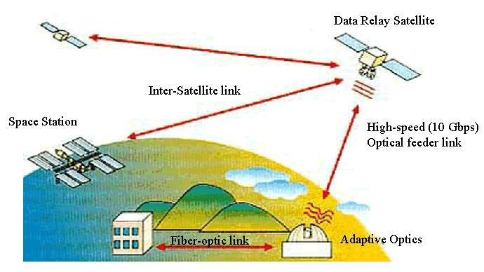
35 Why use optics? Advantages of optical communication (over Radio Frequency) Wider bandwidth Larger capacity Lower power consumption More compact equipment Greater security against eavesdropping Immunity from interference ion/introduction%20(light)/intlight%201%20sm all.jpg
36 1. Optical Communications

37 Lighting the way to a revolution The exponential increase of sharing information is largely due to optical communication technology A few revolutionary technologies based on or effected by optical communication Internet (ex. Ethernet LAN based on Infrared Technology) Cell phones Satellite communication Others? 1966 Dr. Kao and George Hockham: fiber optics to carry information with light
38 Transmitting an audio signal using light In free space (air) Transmitter Circuit Receiver Circuit
39 Modulation Modulation is a way to encode an electromagnetic signal so that it can be transmitted and received. A carrier signal (constant) is changed by the transmitter in some way based on the information to be sent. The receiver then recreates the signal by looking at how the carrier was changed.
40 Modulation 8.0V 7.0V 6.0V 5.0V 4.0V 3.0V Modulating Input signal 2.0V 1.0V 0V -1.0V -2.0V -3.0V Carrier signal -4.0V 0s V(R2:1) V(R1:1) Time 4.0ms Output (modulated carrier) depends on the type of modulation used
41 Modulation Types General Frequency Modulation Amplitude Modulation Pulse Pulse Width Modulation Pulse Position Modulation Pulse Frequency Modulation

42 Amplitude Modulation Frequency of carrier remains constant. Input signal alters amplitude of carrier. Higher input voltage means higher carrier amplitude.

43 Frequency Modulation Amplitude of carrier remains constant. Input signal alters frequency of carrier. Higher input voltage means higher carrier frequency.
44 Pulse Modulation Remember duty cycle definition and equation T on T off Duty _ Cycle Ton T T Ton Toff Duty _ Cycle Pulse_ width Period Carrier has a constant variable Pulse Width Modulation - Period is constant Pulse Position Modulation - Pulse width is constant Pulse Frequency Modulation - Duty cycle is constant Input modulates carrier and effects other two variables

45 Pulse Width Modulation Period of carrier remains constant. Input signal alters duty cycle and pulse width of carrier. Higher input voltage means pulses with longer pulse widths and higher duty cycles.

46 Pulse Position Modulation Pulse width of carrier remains constant. Input signal alters period and duty cycle of carrier. Higher input voltage means pulses with longer periods and lower duty cycles.
47 Pulse Frequency Modulation Duty cycle of carrier remains constant. Input signal alters pulse width and period of carrier. Higher input voltage means pulses with longer pulse widths and longer periods.
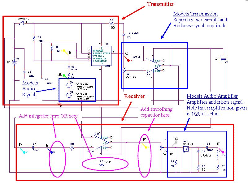
48 2. Initial Design transmitter receiver The initial design for this project is a circuit consisting of a transmitter and a receiver. The circuit is divided into functional blocks. Transmitter: Block A-B and Block B-C Transmission: Block C-D Receiver: Block D-E, Block E-F, Block F-G, and Block G-H You will need to examine each block of the circuit.
49 RRC with variable resistor: Changes sampling frequency (of carrier signal) Transmitter Circuit 5V V1 Rpot 100k C8 330u R3 1k.001uF C2 R2 0 27k 4.7uF C3 Function_Gen_ VCC 8 GND 1 X1 TRIGGER RESET OUTPUT CONTROL THRESHOLD DISCHARGE 555D R19 100ohms LED 3 D1 555 Timer Similar to astable multivibrator configuration: Pin five input alters frequency of pulses
50 Transmitter Circuit: Input and Modulated Output Rpot 100k 5V V1 C8 330u R3 1k.001uF C2 R2 27k 4.7uF C3 Function_Gen_ VCC 8 GND 1 X1 TRIGGER RESET OUTPUT CONTROL THRESHOLD DISCHARGE 3 555D R19 100ohms LED D1 Input signal: function generator or audio 0 Output signal: Light modulation from LED
51 Special Capacitors 5V V1 Rpot 100k C8 330u R3 1k.001uF C2 R2 27k 4.7uF C3 Function_Gen_ VCC 8 GND 1 X1 TRIGGER RESET OUTPUT CONTROL THRESHOLD DISCHARGE 3 555D R19 100ohms LED DC Blocking Capacitor (High Pass Filter) Keeps DC offset from 555 Timer from interfering with input D1 Bypass Capacitor (Low Pass Filter) 0

52 Sample Input and Output When input is higher, pulses are longer When input is lower, pulses are shorter
53 Your signal is what? The type of modulation this circuit creates is most closely categorized as pulse frequency modulation. But the pulse width is also modulated and we will use that feature.
54 Sampling Frequency The pot (used as a variable resistor) controls your sampling frequency Input frequency in audible range max range (20-20kHz) representative range (500-4kHz) Sampling frequency should be between 8kHz and 48kHz to reconstruct sound Input amplitude should not exceed 2Vp-p Function generator can provide 1.2Vp-p
55 Receiver Circuit 56k Add a 100 Ohm resistor in series with the speaker to avoid failures.
56 Receive Light Signal 56k Add a 100 Ohm resistor in series with the speaker to avoid failures.
57 Inverting Amplifier (Pre-Amp) 56k Add a 100 Ohm resistor in series with the speaker to avoid failures.
58 Audio Amplifier 56k Add a 100 Ohm resistor in series with the speaker to avoid failures.
59 Audio Amplifier Details increases gain 10X (not needed) 386 audio amplifier high pass filter volume Add a 100 Ohm resistor in series with the speaker to avoid failures. low pass filter
60 Special Capacitors 56k Not needed Bypass Capacitor DC Blocking Capacitor Add a 100 Ohm resistor in series with the speaker to avoid failures.
61 3. PSpice Model You will compare the performance of your circuit to a PSpice model. The PSpice for the initial design will be given to you. You will use the PSpice to help you make decisions about how to create your final design.
62

63 Comparing Output of Blocks Take pictures of the signal on each side of the circuit block. A on channel 1 and B on channel 2 B on channel 1 and C on channel 2 Take all measurements relative to ground Does the block behave as expected? How does it compare to the PSpice output?
64 10V 5V 0V Comparing Output of Blocks wide-angle view Shows overall shape and size of input and output -5V 8.0ms 8.4ms 8.8ms 9.2ms 9.6ms 10.0ms V(R1:1) V(L1:2) Time 1.0V 0V -1.0V 8.301ms V(R1:1) 8.400ms 8.500ms 8.600ms 8.700ms V(L1:2)/10 Time 8.799ms close-up view Output divided by 10 Shows sampling frequency Shows shape of samples
65 4. Final Design The signal is reconstructed well enough by the initial design that it will be audible. In order to improve the quality of the signal, you will add an integrator, which will more exactly reconstruct it. Types of integrators passive integrator (low pass filter) active integrator (op amp integrator circuit) You will then improve the signal further with a smoothing capacitor.
66 Vin Passive Integration E R1 C1 Vout 500mV 250mV V f out C 0 1 V RC 1 2 RC in dt 0V 1.0Hz 10KHz 100MHz V(R1:2) Frequency Integration works only at high frequencies f >>fc. Unfortunately, your amplitude will also decrease.
67 Active Integration E F 500mV 250mV 0V 1.0Hz 10KHz 100MHz V(R1:2) Frequency V out f 1 R C C i V in 1 2 R dt f C Integration works at f >>fc Your gain goes from -R f /R i to -1/R i C The amplitude of your signal will decrease or increase depending on components
68 Input at A vs. Output at H 10V 5V 0V -5V 8.0ms 8.4ms 8.8ms 9.2ms 9.6ms 10.0ms V(R1:1) V(L1:2) Before addition Time of integrator 4.0V 2.0V 0V -2.0V 8.0ms 8.4ms 8.8ms 9.2ms 9.6ms 10.0ms V(V4:+) V(L1:2) Time After addition of integrator
69 Effect of Smoothing Capacitor D1 V D1N4148 V VOFF = 0 VAMPL = 5v FREQ = 1k V1 R1 1k C1 5u 0 Recall what the smoothing capacitor did to the output of the half wave rectifier.
70 Input at A vs. Output at H 4.0V 2.0V 0V -2.0V 8.0ms 8.4ms 8.8ms 9.2ms 9.6ms 10.0ms V(V4:+) V(L1:2) Before smoothing Time capacitor 2.0V 0V -2.0V 8.0ms 8.4ms 8.8ms 9.2ms 9.6ms 10.0ms V(V4:+) V(L1:2) -v(l1:2) After smoothing Time capacitor
71 Project Packet Initial Data with Function Generator PSpice Mobile Studio plots from circuit Brief Comparison Block Description For Blocks: A-B, A-C, A-D, A-E, A-F, A-G Overall System: A-H Initial Data with Audio Mobile Studio plots from circuit For E-F and A-H
72 Project Packet Final Data (integrator only) with Function Generator PSpice Mobile Studio plots from circuit Brief Comparison For E-F and A-H Final Data (integrator and smoothing) PSpice only PSpice Compare to without smoothing For E-F and A-H
73 Project Packet Final Data with Integrator (and possibly Smoothing) with Audio Mobile Studio plots from circuit For E-F and A-H Extra Credit Mobile Studio picture of A-H with input from function generator and integrated, smoothed output. Indicate values of components and where used.
74 Work in teams Put the transmitter on one protoboard and the receiver on a second. One pair do the transmitter circuit This is the easier circuit, so maybe also start the PSpice simulation. The other pair build the receiver circuit One report for the entire team Report is closer to an experiment report than a project report See details in handout.
Electronic Instrumentation
 Electronic Instrumentation Project 4: Optical Communication Link 1. Optical Communications 2. Initial Design 3. PSpice Model 4. Final Design 5. Project Report Why use optics? Advantages of optical communication
Electronic Instrumentation ENGR-4300 Fall Project 4: Optical Communications Link
 Project 4: Optical Communications Link In this project you will build a transmitter and a receiver circuit. The transmitter circuit uses pulse frequency modulation to create a series of light pulses that
Project 4 Optical Communications Link
 Project 4 Optical Communications Link Pulse Frequency Modulation Figure 1. In this project you will build optical transmitter and receiver circuits. The transmitter circuit uses pulse frequency modulation
ENGR4300 Fall 2005 Test 4A. Name solutions. Section. Question 1 (25 points) Question 2 (25 points) Question 3 (25 points) Question 4 (25 points)
 Question 2 (25 points) Question 3 (25 points) Question 4 (25 points)") ENGR4300 Fall 2005 Test 4A Name solutions Section Question 1 (25 points) Question 2 (25 points) Question 3 (25 points) Question 4 (25 points) Total (100 points): Please do not write on the crib sheets.
ENGR4300 Fall 2005 Test 4A Name solutions Section Question 1 (25 points) Question 2 (25 points) Question 3 (25 points) Question 4 (25 points) Total (100 points): Please do not write on the crib sheets.
ENGR4300 Fall 2005 Test 4A. Name. Section. Question 1 (25 points) Question 2 (25 points) Question 3 (25 points) Question 4 (25 points)
 Question 2 (25 points) Question 3 (25 points) Question 4 (25 points)") ENGR4300 Fall 2005 Test 4A Name Section Question 1 (25 points) Question 2 (25 points) Question 3 (25 points) Question 4 (25 points) Total (100 points): Please do not write on the crib sheets. On all questions:
ENGR4300 Fall 2005 Test 4A Name Section Question 1 (25 points) Question 2 (25 points) Question 3 (25 points) Question 4 (25 points) Total (100 points): Please do not write on the crib sheets. On all questions:
Class #9: Experiment Diodes Part II: LEDs
 Class #9: Experiment Diodes Part II: LEDs Purpose: The objective of this experiment is to become familiar with the properties and uses of LEDs, particularly as a communication device. This is a continuation
ENGR4300 Test 3A Fall 2002
 1. 555 Timer (20 points) Figure 1: 555 Timer Circuit For the 555 timer circuit in Figure 1, find the following values for R1 = 1K, R2 = 2K, C1 = 0.1uF. Show all work. a) (4 points) T1: b) (4 points) T2:
DESIGN OF AN ANALOG FIBER OPTIC TRANSMISSION SYSTEM
 DESIGN OF AN ANALOG FIBER OPTIC TRANSMISSION SYSTEM OBJECTIVE To design and build a complete analog fiber optic transmission system, using light emitting diodes and photodiodes. INTRODUCTION A fiber optic
ENGR-2300 Electronic Instrumentation Quiz 3 Spring 2015
 ENGR-23 Electronic Instrumentation Quiz 3 Spring 215 On all questions: SHOW ALL WORK. BEGIN WITH FORMULAS, THEN SUBSTITUTE VALUES AND UNITS. No credit will be given for answers that appear without justification.
ENGR4300 Spring 2006 Test 4B. Name solution. Section 3 and 4. Question 1 (25 points) This is worth 20 not 25
 This is worth 20 not 25") ENGR4300 Spring 2006 Test 4B Name solution Section 3 and 4 Question 1 (25 points) This is worth 20 not 25 Question 2 (15 points) This is worth 20 not 15 Question 3 (20 points) Question 4 (20 points) Question
ENGR4300 Spring 2006 Test 4B Name solution Section 3 and 4 Question 1 (25 points) This is worth 20 not 25 Question 2 (15 points) This is worth 20 not 15 Question 3 (20 points) Question 4 (20 points) Question
Electronic Instrumentation ENGR-4300 Fall 2002 Project 2: Optical Communications Link
 Project 2: Optical Communications Link For this project, each group will build a transmitter circuit and a receiver circuit. It is suggested that 1 or 2 students build and test the individual components
UNIVERSITY OF NORTH CAROLINA AT CHARLOTTE. Department of Electrical and Computer Engineering
 UNIVERSITY OF NORTH CAROLINA AT CHARLOTTE Department of Electrical and Computer Engineering Experiment No. 2 - Semiconductor Diodes Overview: In this lab session students will investigate I-V characteristics
ENGR-4300 Fall 2008 Test 4. Name SOLUTION. Section 1(MR 8:00) 2(TF 2:00) (circle one) Question I (20 points) Question II (20 points)
 2(TF 2:00) (circle one) Question I (20 points) Question II (20 points)") ENGR-43 Fall 28 Test 4 Name SOLUTION Section 1(MR 8:) 2(TF 2:) (circle one) Question I (2 points) Question II (2 points) Question III (15 points) Question IV (2 points) Question V (25 points) Total (1
ENGR-43 Fall 28 Test 4 Name SOLUTION Section 1(MR 8:) 2(TF 2:) (circle one) Question I (2 points) Question II (2 points) Question III (15 points) Question IV (2 points) Question V (25 points) Total (1
The preferred Exercise is shown in Exercises 5B or 5C.
 ECE 231 Laboratory Exercise 5A The preferred Exercise is shown in Exercises 5B or 5C. Laboratory Group (Names) OBJECTIVES Validate the Schottky diode equation. Calculate the dc and dynamic (ac) resistance
EXPERIMENT 7: DIODE CHARACTERISTICS AND CIRCUITS 10/24/10
 DIODE CHARACTERISTICS AND CIRCUITS EXPERIMENT 7: DIODE CHARACTERISTICS AND CIRCUITS 10/24/10 In this experiment we will measure the I vs V characteristics of Si, Ge, and Zener p-n junction diodes, and
Spring Diodes (25 points) In the figure below, each of the diodes turns on at between 0.7 volts and R=2k.
 In the figure below, each of the diodes turns on at between 0.7 volts and R=2k.") Spring 2002 2. Diodes (25 points) In the figure below, each of the diodes turns on at between 0.7 volts and R=2k. 1. Give the voltage at out for each of the following values of the input voltage, in (2
Spring 2002 2. Diodes (25 points) In the figure below, each of the diodes turns on at between 0.7 volts and R=2k. 1. Give the voltage at out for each of the following values of the input voltage, in (2
Table of Contents. iii
 Table of Contents Subject Page Experiment 1: Diode Characteristics... 1 Experiment 2: Rectifier Circuits... 7 Experiment 3: Clipping and Clamping Circuits 17 Experiment 4: The Zener Diode 25 Experiment
LED lecture. Wei Chih Wang University of Washington
 LED lecture Wei Chih Wang University of Washington Linear and Nonlinear electronics current voltage Vaccum tube (i.e. type 2A3) voltage Thermistor (large negative temperature coefficient of resistivity)
Electronic Instrumentation ENGR-4300 Fall 2004 Section Experiment 7 Introduction to the 555 Timer, LEDs and Photodiodes
 Experiment 7 Introduction to the 555 Timer, LEDs and Photodiodes Purpose: In this experiment, we learn a little about some of the new components which we will use in future projects. The first is the 555
ENGR4300 Test 4A Spring 2005
 Question 1 Diodes Assume that the forward bias threshold voltage for the diode in the circuit is 0.7V. A. Consider the following circuit a) What type of diode circuit is the circuit above? (1 pt) half
Diode Limiters or Clipper Circuits
 Diode Limiters or Clipper Circuits Circuits which are used to clip off portions of signal voltages above or below certain levels are called limiters or clippers. Types of Clippers Positive Clipper Negative
ENGR-4300 Spring 2009 Test 4. Name SOLUTION. Section 1(MR 8:00) 2(TF 2:00) 3(MR 6:00) (circle one) Question I (20 points) Question II (20 points)
 2(TF 2:00) 3(MR 6:00) (circle one) Question I (20 points) Question II (20 points)") ENGR-43 Spring 29 Test 4 Name SOLUTION Section 1(MR 8:) 2(TF 2:) 3(MR 6:) (circle one) Question I (2 points) Question II (2 points) Question III (15 points) Question IV (25 points) Question V (2 points)
ENGR-43 Spring 29 Test 4 Name SOLUTION Section 1(MR 8:) 2(TF 2:) 3(MR 6:) (circle one) Question I (2 points) Question II (2 points) Question III (15 points) Question IV (25 points) Question V (2 points)
ENGR-2300 Electronic Instrumentation Quiz 4 Fall 2012 Name
 ENGR-23 Quiz 4 Fall 212 ENGR-23 Electronic Instrumentation Quiz 4 Fall 212 Name Question I (25 points) Question II (25 points) Question III (25 points) Question IV (25 points) Total (1 points) On all questions:
LABORATORY EXPERIMENT. Infrared Transmitter/Receiver
 LABORATORY EXPERIMENT Infrared Transmitter/Receiver (Note to Teaching Assistant: The week before this experiment is performed, place students into groups of two and assign each group a specific frequency
ENGR-4300 Fall 2006 Project 3 Project 3 Build a 555-Timer
 ENGR-43 Fall 26 Project 3 Project 3 Build a 555-Timer For this project, each team, (do this as team of 4,) will simulate and build an astable multivibrator. However, instead of using the 555 timer chip,
the reactance of the capacitor, 1/2πfC, is equal to the resistance at a frequency of 4 to 5 khz.
 EXPERIMENT 12 INTRODUCTION TO PSPICE AND AC VOLTAGE DIVIDERS OBJECTIVE To gain familiarity with PSPICE, and to review in greater detail the ac voltage dividers studied in Experiment 14. PROCEDURE 1) Connect
Electric Circuit Fall 2017 Lab3 LABORATORY 3. Diode. Guide
 LABORATORY 3 Diode Guide Diodes Overview Diodes are mostly used in practice for emitting light (as Light Emitting Diodes, LEDs) or controlling voltages in various circuits. Typical diode packages in same
Optical Modulation and Frequency of Operation
 Optical Modulation and Frequency of Operation Developers AB Overby Objectives Preparation Background The objectives of this experiment are to describe and illustrate the differences between frequency of
Federal Urdu University of Arts, Science & Technology Islamabad Pakistan SECOND SEMESTER ELECTRONICS - I
 SECOND SEMESTER ELECTRONICS - I BASIC ELECTRICAL & ELECTRONICS LAB DEPARTMENT OF ELECTRICAL ENGINEERING Prepared By: Checked By: Approved By: Engr. Yousaf Hameed Engr. M.Nasim Khan Dr.Noman Jafri Lecturer
Difference between BJTs and FETs. Junction Field Effect Transistors (JFET)
") Difference between BJTs and FETs Transistors can be categorized according to their structure, and two of the more commonly known transistor structures, are the BJT and FET. The comparison between BJTs
Difference between BJTs and FETs Transistors can be categorized according to their structure, and two of the more commonly known transistor structures, are the BJT and FET. The comparison between BJTs
Diodes Rectifiers, Zener diodes light emitting diodes, laser diodes photodiodes, optocouplers
 Diodes Rectifiers, Zener diodes light emitting diodes, laser diodes photodiodes, optocouplers Prepared by Scott Robertson Fall 2007 Physics 3330 1 Impurity-doped semiconductors Semiconductors (Ge, Si)
The George Washington University School of Engineering and Applied Science Department of Electrical and Computer Engineering ECE 20 - LAB
 The George Washington University School of Engineering and Applied Science Department of Electrical and Computer Engineering ECE 20 - LAB Components: Experiment # 1 Solid State Diodes Testing & Characterization
Diode Applications Half-Wave Rectifying
 Lab 5 Diode Applications Half-Wave ectifying Objectives: Study the half-wave rectifying and smoothing with a capacitor for a simple diode circuit. Study the use of a Zener diode in a circuit with an AC
Class #8: Experiment Diodes Part I
 Class #8: Experiment Diodes Part I Purpose: The objective of this experiment is to become familiar with the properties and uses of diodes. We used a 1N914 diode in two previous experiments, but now we
Government Polytechnic Muzaffarpur Name of the Lab: Applied Electronics Lab
 Government Polytechnic Muzaffarpur Name of the Lab: Applied Electronics Lab Subject Code: 1620408 Experiment-1 Aim: To obtain the characteristics of field effect transistor (FET). Theory: The Field Effect
Concepts to be Reviewed
 Introductory Medical Device Prototyping Analog Circuits Part 3 Operational Amplifiers, http://saliterman.umn.edu/ Department of Biomedical Engineering, University of Minnesota Concepts to be Reviewed Operational
Physics 281 EXPERIMENT 7 I-V Curves of Non linear Device
 Physics 281 EXPERIMENT 7 I-V Curves of Non linear Device Print this page to start your lab report (1 copy) Bring a diskette to save your data. OBJECT: To study the method of obtaining the characteristics
Project 3 Build a 555-Timer
 Project 3 Build a 555-Timer For this project, each group will simulate and build an astable multivibrator. However, instead of using the 555 timer chip, you will have to use the devices you learned about
UNIT-V: WAVEFORM GENERATORS AND SPECIAL FUNCTION ICs. PARTA (2 Marks)
") UNIT-V: WAVEFORM GENERATORS AND SPECIAL FUNCTION ICs PARTA (2 Marks) 1. Define line regulation.[auc April 2004] It is defined as the percentage change in the output voltage from a change in the input voltage.
UNIT-V: WAVEFORM GENERATORS AND SPECIAL FUNCTION ICs PARTA (2 Marks) 1. Define line regulation.[auc April 2004] It is defined as the percentage change in the output voltage from a change in the input voltage.
ENGR4300 Test 3A and 3B Fall 2003
 Question 1 -- Astable Multivibrator R1 8 X1 18 1 1 2 U3 R2 TOPEN = 0 2 4 5 6 7 CC TRIGGER RESETOUTPUT CONTROL THRESHOLD DISCHARGE GND 555D R3 1Meg C1 C2 10uF.01uF 1 3 0 The circuit above has been simulated
LABORATORY 8 DIODE CIRCUITS
 LABORATORY 8 DIODE CIRCUITS A solid state diode consists of a junction of either dissimilar semiconductors (pn junction diode) or a metal and a semiconductor (Schottky barrier diode). Regardless of the
Basic Electronic Devices and Circuits EE 111 Electrical Engineering Majmaah University 2 nd Semester 1432/1433 H. Chapter 2. Diodes and Applications
 Basic Electronic Devices and Circuits EE 111 Electrical Engineering Majmaah University 2 nd Semester 1432/1433 H Chapter 2 Diodes and Applications 1 Diodes A diode is a semiconductor device with a single
ETEK TECHNOLOGY CO., LTD.
 Trainer Model: ETEK DCS-6000-07 FSK Modulator ETEK TECHNOLOGY CO., LTD. E-mail: etek21@ms59.hinet.net mlher@etek21.com.tw http: // www.etek21.com.tw Digital Communication Systems (ETEK DCS-6000) 13-1:
LIC & COMMUNICATION LAB MANUAL
 LIC & Communication Lab Manual LIC & COMMUNICATION LAB MANUAL FOR V SEMESTER B.E (E& ( E&C) (For private circulation only) NAME: DEPARTMENT OF ELECTRONICS & COMMUNICATION SRI SIDDHARTHA INSTITUTE OF TECHNOLOGY
RC Servo Interface. Figure Bipolar amplifier connected to a large DC motor
 The bipolar amplifier is well suited for controlling motors for vehicle propulsion. Figure 12-45 shows a good-sized 24VDC motor that runs nicely on 13.8V from a lead acid battery based power supply. You
Sirindhorn International Institute of Technology Thammasat University at Rangsit
 Sirindhorn International Institute of Technology Thammasat University at Rangsit School of Information, Computer and Communication Technology COURSE : ECS 204 Basic Electrical Engineering Lab INSTRUCTOR
Module 04.(B1) Electronic Fundamentals
 Electronic Fundamentals") 1.1a. Semiconductors - Diodes. Module 04.(B1) Electronic Fundamentals Question Number. 1. What gives the colour of an LED?. Option A. The active element. Option B. The plastic it is encased in. Option
1.1a. Semiconductors - Diodes. Module 04.(B1) Electronic Fundamentals Question Number. 1. What gives the colour of an LED?. Option A. The active element. Option B. The plastic it is encased in. Option
Week 8 AM Modulation and the AM Receiver
 Week 8 AM Modulation and the AM Receiver The concept of modulation and radio transmission is introduced. An AM receiver is studied and the constructed on the prototyping board. The operation of the AM
Experiments in Photonics
 Experiments in Photonics Section 3: Electronics & Photonics An integrated electronic/photonic device. Photograph courtesy of Quantum Optics Group, Australian National University Minilabs 2006 1 Electronics
EE283 Electrical Measurement Laboratory Laboratory Exercise #7: Digital Counter
 EE283 Electrical Measurement Laboratory Laboratory Exercise #7: al Counter Objectives: 1. To familiarize students with sequential digital circuits. 2. To show how digital devices can be used for measurement
Chapter 5: Diodes. I. Theory. Chapter 5: Diodes
 Chapter 5: Diodes This week we will explore another new passive circuit element, the diode. We will also explore some diode applications including conversion of an AC signal into a signal that never changes
Shankersinh Vaghela Bapu Institute of Technology INDEX
 Shankersinh Vaghela Bapu Institute of Technology Diploma EE Semester III 3330905: ELECTRONIC COMPONENTS AND CIRCUITS INDEX Sr. No. Title Page Date Sign Grade 1 Obtain I-V characteristic of Diode. 2 To
Massachusetts Institute of Technology MIT
 Massachusetts Institute of Technology MIT Real Time Wireless Electrocardiogram (ECG) Monitoring System Introductory Analog Electronics Laboratory Guilherme K. Kolotelo, Rogers G. Reichert Cambridge, MA
ITT Technical Institute. ET215 Devices I Chapter 2 Sections
 ITT Technical Institute ET215 Devices I Chapter 2 Sections 2.8-2.10 Chapter 2 Section 2.8 Special-Purpose Diodes The preceding discussions of diodes has focused on applications that exploit the fact that
Figure 1: Diode Measuring Circuit
 Diodes, Page 1 Diodes V-I Characteristics signal diode Measure the voltage-current characteristic of a standard signal diode, the 1N914, using the circuit shown in Figure 1 below. The purpose of the back-to-back
Infrared Communications Lab
 Infrared Communications Lab This lab assignment assumes that the student knows about: Ohm s Law oltage, Current and Resistance Operational Amplifiers (See Appendix I) The first part of the lab is to develop
3.4. Reverse Breakdown Region Zener Diodes In the breakdown region Very steep i-v curve Almost constant voltage drop Used for voltage regulator
 3.4. Reverse Breakdown Region Zener Diodes In the breakdown region Very steep i-v curve Almost constant voltage drop Used for voltage regulator Voltage regulator Provide a constant dc output voltage If
Assume availability of the following components to DESIGN and DRAW the circuits of the op. amp. applications listed below:
 ========================================================================================== UNIVERSITY OF SOUTHERN MAINE Dept. of Electrical Engineering TEST #3 Prof. M.G.Guvench ELE343/02 ==========================================================================================
ECEN Network Analysis Section 3. Laboratory Manual
 ECEN 3714----Network Analysis Section 3 Laboratory Manual LAB 07: Active Low Pass Filter Oklahoma State University School of Electrical and Computer Engineering. Section 3 Laboratory manual - 1 - Spring
Diodes. Analog Electronics Lesson 4. Objectives and Overview:
 Analog Electronics Lesson 4 Diodes Objectives and Overview: This lesson will introduce p- and n-type material, how they form a junction that rectifies current, and familiarize you with basic p-n junction
AE103 ELECTRONIC DEVICES & CIRCUITS DEC 2014
 Q.2 a. State and explain the Reciprocity Theorem and Thevenins Theorem. a. Reciprocity Theorem: If we consider two loops A and B of network N and if an ideal voltage source E in loop A produces current
Circuit Components Lesson 4 From: Emergency Management Ontario
 4.1 Amplifier Fundamentals The role of a amplifier is to produce an output which is an enlarged reproduction of the features of the signal fed into the input. The increase in signal by an amplifier is
Fundamentals of Microelectronics
 Fundamentals of Microelectronics CH1 Why Microelectronics? CH2 Basic Physics of Semiconductors CH3 Diode Circuits CH4 Physics of Bipolar Transistors CH5 Bipolar Amplifiers CH6 Physics of MOS Transistors
Experiments in Analog Electronics
 Ministry of Higher Education and Scientific Research University of Technology Department of Electrical Engineering Analog Electronics Laboratory Experiments in Analog Electronics By Firas Mohammed Ali
Facility of Engineering. Biomedical Engineering Department. Medical Electronic Lab BME (317) Pre-Report Forms
 Pre-Report Forms") Facility of Engineering Biomedical Engineering Department Medical Electronic Lab BME (317) Pre-Report Forms Prepared by Eng.Hala Amari Spring 2014 Facility of Engineering Biomedical Engineering Department
Facility of Engineering Biomedical Engineering Department Medical Electronic Lab BME (317) Pre-Report Forms Prepared by Eng.Hala Amari Spring 2014 Facility of Engineering Biomedical Engineering Department
THIRD SEMESTER ELECTRONICS - II BASIC ELECTRICAL & ELECTRONICS LAB DEPARTMENT OF ELECTRICAL ENGINEERING
 THIRD SEMESTER ELECTRONICS - II BASIC ELECTRICAL & ELECTRONICS LAB DEPARTMENT OF ELECTRICAL ENGINEERING Prepared By: Checked By: Approved By: Engr. Saqib Riaz Engr. M.Nasim Khan Dr.Noman Jafri Lecturer
Diodes and Applications
 Diodes and Applications Diodes and Applications 2 1 Diode Operation 2 2 Voltage-Current (V-I) Characteristics 2 3 Diode Models 2 4 Half-Wave Rectifiers 2 5 Full-Wave Rectifiers 2 6 Power Supply Filters
ECE 2274 Diode Basics and a Rectifier Completed Prior to Coming to Lab
 ECE 2274 Diode Basics and a Rectifier Completed Prior to Coming to Lab Perlab: Part I I-V Characteristic Curve for the 1. Construct the circuit shown in figure 1. Using a DC Sweep, simulate in LTspice
Concepts to be Covered
 Introductory Medical Device Prototyping Analog Circuits Part 2 Semiconductors, http://saliterman.umn.edu/ Department of Biomedical Engineering, University of Minnesota Concepts to be Covered Semiconductors
EE 110 Introduction to Engineering & Laboratory Experience Saeid Rahimi, Ph.D. Lab 6 Diodes: Half-Wave and Full-Wave Rectifiers Converting AC to DC
 EE 110 Introduction to Engineering & Laboratory Experience Saeid Rahimi, Ph.D. Lab 6 Diodes: Half-Wave and Full-Wave Rectifiers Converting C to DC The process of converting a sinusoidal C voltage to a
Application Note AN-3006 Optically Isolated Phase Controlling Circuit Solution
 www.fairchildsemi.com Application Note AN-3006 Optically Isolated Phase Controlling Circuit Solution Introduction Optocouplers simplify logic isolation from the ac line, power supply transformations, and
Revised: Summer 2010
 EE 2274 PRE-LAB EXPERIMENT 5 DIODE OR GATE & CLIPPING CIRCUIT COMPLETE PRIOR TO COMING TO LAB Part I: 1. Design a diode, Figure 1 OR gate in which the maximum input current,, Iin is less than 5mA. Show
Facility of Engineering. Biomedical Engineering Department. Medical Electronic Lab BME (317) Post-lab Forms
 Post-lab Forms") Facility of Engineering Biomedical Engineering Department Medical Electronic Lab BME (317) Post-lab Forms Prepared by Eng.Hala Amari Spring 2014 Facility of Engineering Biomedical Engineering Department
Facility of Engineering Biomedical Engineering Department Medical Electronic Lab BME (317) Post-lab Forms Prepared by Eng.Hala Amari Spring 2014 Facility of Engineering Biomedical Engineering Department
Lecture (09) Bipolar Junction Transistor 3
 Bipolar Junction Transistor 3") Lecture (09) Bipolar Junction Transistor 3 By: Dr. Ahmed ElShafee ١ I THE BJT AS AN AMPLIFIER Amplification is the process of linearly increasing the amplitude of an electrical signal and is one of the
Lecture (09) Bipolar Junction Transistor 3 By: Dr. Ahmed ElShafee ١ I THE BJT AS AN AMPLIFIER Amplification is the process of linearly increasing the amplitude of an electrical signal and is one of the
1) Consider the circuit shown in figure below. Compute the output waveform for an input of 5kHz
 Consider the circuit shown in figure below. Compute the output waveform for an input of 5kHz") ) Consider the circuit shown in figure below. Compute the output waveform for an input of 5kHz Solution: a) Input is of constant amplitude of 2 V from 0 to 0. ms and 2 V from 0. ms to 0.2 ms. The output
) Consider the circuit shown in figure below. Compute the output waveform for an input of 5kHz Solution: a) Input is of constant amplitude of 2 V from 0 to 0. ms and 2 V from 0. ms to 0.2 ms. The output
After performing this experiment, you should be able to:
 Objectives: After performing this experiment, you should be able to: Demonstrate the strengths and weaknesses of the two basic rectifier circuits. Draw the output waveforms for the two basic rectifier
BME/ISE 3512 Laboratory - Three Diode (1N4001)
") BME/ISE 3512 Laboratory Three Diode (1N4001) Learning Objectives: Understand the concept of PN junction diodes, their application as rectifiers, the nature and application of halfwave and fullwave rectifiers,
BME/ISE 3512 Laboratory Three Diode (1N4001) Learning Objectives: Understand the concept of PN junction diodes, their application as rectifiers, the nature and application of halfwave and fullwave rectifiers,
CHAPTER 1 DIODE CIRCUITS. Semiconductor act differently to DC and AC currents
 CHAPTER 1 DIODE CIRCUITS Resistance levels Semiconductor act differently to DC and AC currents There are three types of resistances 1. DC or static resistance The application of DC voltage to a circuit
EE 3305 Lab I Revised July 18, 2003
 Operational Amplifiers Operational amplifiers are high-gain amplifiers with a similar general description typified by the most famous example, the LM741. The LM741 is used for many amplifier varieties
Chapter 1: Semiconductor Diodes
 Chapter 1: Semiconductor Diodes Diodes The diode is a 2-terminal device. A diode ideally conducts in only one direction. 2 Diode Characteristics Conduction Region Non-Conduction Region The voltage across
Mechatronics and Measurement. Lecturer:Dung-An Wang Lecture 2
 Mechatronics and Measurement Lecturer:Dung-An Wang Lecture 2 Lecture outline Reading:Ch3 of text Today s lecture Semiconductor 2 Diode 3 4 Zener diode Voltage-regulator diodes. This family of diodes exhibits
Electronics EECE2412 Spring 2016 Exam #1
 Electronics EECE2412 Spring 2016 Exam #1 Prof. Charles A. DiMarzio Department of Electrical and Computer Engineering Northeastern University 18 February 2016 File:12140/exams/exam1 Name: : Row # : Seat
LINEAR IC APPLICATIONS
 1 B.Tech III Year I Semester (R09) Regular & Supplementary Examinations December/January 2013/14 1 (a) Why is R e in an emitter-coupled differential amplifier replaced by a constant current source? (b)
Questions about Circuit Functionality. Fall 2004 Question 5 -- Transformers (15 points)
") Questions about Circuit Functionality Fall 2004 Question 5 -- Transformers (15 points) Below is a circuit containing a transformer and an op-amp circuit you should recognize from the homework and experiment
Questions about Circuit Functionality Fall 2004 Question 5 -- Transformers (15 points) Below is a circuit containing a transformer and an op-amp circuit you should recognize from the homework and experiment
GATE SOLVED PAPER - IN
 YEAR 202 ONE MARK Q. The i-v characteristics of the diode in the circuit given below are : v -. A v 0.7 V i 500 07 $ = * 0 A, v < 0.7 V The current in the circuit is (A) 0 ma (C) 6.67 ma (B) 9.3 ma (D)
Touchless Control: Hand Motion Triggered Light Timer
 Touchless Control: Hand Motion Triggered Light Timer 6.101 Final Project Report Justin Graves Spring 2018 1 Introduction Often times when you enter a new room you are troubled with finding the light switch
Electrical and Electronic Laboratory Faculty of Engineering Chulalongkorn University. Semiconductor Diode (SD)
") 2141274 Electrical and Electronic Laboratory Faculty of Engineering Chulalongkorn University Semiconductor Diode (SD) Contents A. Introduction 1. History 2. Thermionic or gaseous state diodes 3. Semiconductor
2141274 Electrical and Electronic Laboratory Faculty of Engineering Chulalongkorn University Semiconductor Diode (SD) Contents A. Introduction 1. History 2. Thermionic or gaseous state diodes 3. Semiconductor
Circuit operation Let s look at the operation of this single diode rectifier when connected across an alternating voltage source v s.
 Diode Rectifier Circuits One of the important applications of a semiconductor diode is in rectification of AC signals to DC. Diodes are very commonly used for obtaining DC voltage supplies from the readily
LABORATORY 3: Transient circuits, RC, RL step responses, 2 nd Order Circuits
 LABORATORY 3: Transient circuits, RC, RL step responses, nd Order Circuits Note: If your partner is no longer in the class, please talk to the instructor. Material covered: RC circuits Integrators Differentiators
Homework Assignment 06
 Question 1 (2 points each unless noted otherwise) Homework Assignment 06 1. True or false: when transforming a circuit s diagram to a diagram of its small-signal model, we replace dc constant current sources
Tektronix Courseware. Academic Labs. Sample Labs from Popular Electrical and Electronics Engineering Curriculum
 Tektronix Courseware Academic Labs Sample Labs from Popular Electrical and Electronics Engineering Curriculum March 3, 2014 HalfWaveRectifier -- Overview OBJECTIVES After performing this lab exercise,
Lab 2 Revisited Exercise
 Lab 2 Revisited Exercise +15V 100k 1K 2N2222 Wire up led display Note the ground leads LED orientation 6.091 IAP 2008 Lecture 3 1 Comparator, Oscillator +5 +15 1k 2 V- 7 6 Vin 3 V+ 4 V o Notice that power
REV NO EXPERIMENT NO 1 AIM: To study the PN junction diode characteristics under Forward & Reverse bias conditions. APPARATUS REQUIRED:
 KARNAL INSTITUTE OF TECHNOLOGY & MANAGEMENT KUNJPURA, KARNAL LAB MANUAL OF ------- SUBJECT CODE DATE OF ISSUE: SEMESTER: BRANCH: REV NO EXPERIMENT NO 1 AIM: To study the PN junction diode characteristics
Analog Circuits Part 3 Operational Amplifiers
 Introductory Medical Device Prototyping Analog Circuits Part 3 Operational Amplifiers, http://saliterman.umn.edu/ Department of Biomedical Engineering, University of Minnesota Concepts to be Reviewed Operational
University of North Carolina, Charlotte Department of Electrical and Computer Engineering ECGR 3157 EE Design II Fall 2009
 University of North Carolina, Charlotte Department of Electrical and Computer Engineering ECGR 3157 EE Design II Fall 2009 Lab 1 Power Amplifier Circuits Issued August 25, 2009 Due: September 11, 2009
ENGR 201 Homework, Fall 2018
 Chapter 1 Voltage, Current, Circuit Laws (Selected contents from Chapter 1-3 in the text book) 1. What are the following instruments? Draw lines to match them to their cables: Fig. 1-1 2. Complete the
DEPARTMENT OF ELECTRICAL ENGINEERING LAB WORK EE301 ELECTRONIC CIRCUITS
 DEPARTMENT OF ELECTRICAL ENGINEERING LAB WORK EE301 ELECTRONIC CIRCUITS EXPERIMENT : 4 TITLE : 555 TIMERS OUTCOME : Upon completion of this unit, the student should be able to: 1. gain experience with
Final Project Stereo Audio Amplifier Final Report
 The George Washington University School of Engineering and Applied Science Department of Electrical and Computer Engineering Final Project Stereo Audio Amplifier Final Report Daniel S. Boucher ECE 20-32,
Electronics 1 Lab (CME 2410) School of Informatics & Computing German Jordanian University Laboratory Experiment (10) Junction FETs
 School of Informatics & Computing German Jordanian University Laboratory Experiment (10) Junction FETs") Electronics 1 Lab (CME 2410) School of Informatics & Computing German Jordanian University Laboratory Experiment (10) 1. Objective: Junction FETs - the operation of a junction field-effect transistor (J-FET)
Electronics 1 Lab (CME 2410) School of Informatics & Computing German Jordanian University Laboratory Experiment (10) 1. Objective: Junction FETs - the operation of a junction field-effect transistor (J-FET)
Electronics. RC Filter, DC Supply, and 555
 Electronics RC Filter, DC Supply, and 555 0.1 Lab Ticket Each individual will write up his or her own Lab Report for this two-week experiment. You must also submit Lab Tickets individually. You are expected