ADAPTIVE DECISION FEEDBACK EQUALIZATION FOR MULTI-Gbps DATA LINKS
|
|
|
- Brittany Johns
- 6 years ago
- Views:
Transcription
1 ADAPTIVE DECISION FEEDBACK EQUALIZATION FOR MULTI-Gbps DATA LINKS by Alaa R. Abdullah Bacelor of Science, University of Technology, Baghdad, Iraq, 1989 Master of Science, Ryerson University, Toronto, Canada, 2010 A dissertation presented to Ryerson University in partial fulfillment of the requirement for the degree of Doctor of Philosophy in the Program of Electrical and Computer Engineering Toronto, Ontario, Canada, 2014 c Alaa R. Abdullah, 2014
2 Author s Declaration For Electronic Submission of A Dissertation I hereby declare that I am the sole author of this dissertation. This is a true copy of the dissertation, including any required final revisions, as accepted by my examiners. I authorize Ryerson University to lend this dissertation to other institutions or individuals for the purpose of scholarly research. I further authorize Ryerson University to reproduce this dissertation by photocopying or by other means, in total or in part, at the request of other institutions or individuals for the purpose of scholarly research. I understand that my dissertation may be made electronically available to the public. ii
3 Abstract Adaptive Decision Feedback Equalization For Multi-Gbps Data Links c Alaa R. Abdullah, 2014 Doctor of Philosophy Electrical and Computer Engineering Ryerson University Channel equalization combats the effects of the imperfection of wire channels. This dissertation deals with adaptive decision feedback channel equalization. The dissertation starts with an in depth study of the challenges encountered in the design of adaptive DFE and techniques that address these challenges. Various 2-dimensional eye-opening monitors (EOMs) based adaptive DFE are proposed and implemented. A novel 2-dimensional hexagon EOM is proposed and its effectiveness is validated using simulation. A simplified and power efficient 2-dimensional hexagon EOM is also introduced. Both EOMs are capable of differentiating the severity of the violation of the minimum eye-opening so as to allow the DFE to take different actions adaptively and achieve desired eye-opening more rapidly. A maximum-jitter EOM-based adaptive DFE is also introduced to greatly reduce system complexity. The adaptive DFE is taped out in a 130nm 1.2V CMOS technology and finally an improved adaptive engine that outperforms DFE utilizing sign-sign least-mean-square is proposed. iii
4 Acknowledgements I am heartily thankful to my supervisor, Professor Fei Yuan, for his wonderful guidance throughout all the stages of my PhD studies. Without his continued encouragement and support, this dissertation would not have been possible. I am also thankful for the excellent example Professor Fei Yuan has provided as a successful researcher, wonderful teacher and role model. I wish to express my sincere gratitude to my co-supervisor Dr. Andy Ye who helped and supported me in every aspect during the completion of my studies. I offer my regards and blessings to my colleagues and staff at Integrated Circuits and Systems Research Group at Ryerson University who provided me with valuable technical supports during my studies. Last but not least, I would like to gratefully acknowledge the financial support of Ryerson University especially Electrical and Computer Engineering department and Ontario Graduate Scholarship OGS for their financial support during my studies. iv
5 Dedication To my wonderful wife, daughter and sons, Nissreen, Nursan, Hussin, Yousif and Saif, for their unconditional love, enormous support and continuous encouragement... v
6 Contents 1 Introduction Motivation Objective of The Dissertation Chapter Organization Inter-Symbol Interference Channel Equalization Near-End Channel Equalization Far-End Channel Equalization Decision Feedback Equalization Chapter Summary Contributions of The Dissertation Organization of The Dissertation Design Challenges in DFE Bit Error Rate Test Timing Constraints Timing Alignment Error Propagation Calibration of Slicer Delay Cells Arithmetic Operation Channels with Severe Dispersity vi
7 2.9 Power Consumption Adaptive Decision Feedback Equalization Least-Mean-Square Adaptive DFE Eye-Opening Adaptive DFE Jitter-Based Adaptive DFE Comparison Chapter Summary Dimensional Hexagon Eye-Opening Monitor Eye-Opening Monitors One-Dimensional EOMs Two-Dimensional EOMs Jitter-Based EOMs Eye-Pattern Monitors Proposed Two-Dimensional EOM Drawbacks of Rectangular EOM Diamond EOM Hexagon EOM Discussion Implementation Chapter Summary Dimensional Half-Hexagon Eye- Opening Monitor Half Hexagon Eye-Opening Monitor Implementation Simulation Results Chapter Summary Adaptive DFE Uing 2-Dimensional Hexagon EOM The Principle vii
8 5.2 The Algorithm Implementation The Architecture Slicer Error Detection Unit Digital-To-Analog Converter XOR Gate Simulation Results Chapter Summary Maximum-Jitter Adaptive DFE Maximum-Jitter Adaptive DFE The Principle Implementation Error Detection Unit Digital-to-Analog Converter Simulation Results Drawbacks of Adaptive DFE Using SS-LMS or EOM Drawbacks of Adaptive DFE Using SS-LMS Drawbacks of Adaptive DFE Using EOM The Solution Simulation Results Chapter Summary Conclusions and Future Work Conclusions Future Work List of Publications viii
9 List of Figures 1.1 Dependence of data rate on the minimum channel length of MOS transistors (a) Frequency response of a 30 trace on a Nelco SI board [1]. (b) Frequency response of a 16 Tyco legancy backplane with two daughter cards [4]. (c,d) Frequency response and impulse response of a highly reflective backplane [5] (Copyright c IEEE) Pre-cursors, main cursor, and post-cursors of data symbol at the far end of a wire channel Inter-symbol interference in multi symbols Near-end channel equalization with first-order pre-emphasis. The added preemphasis tap shortens the duration of the received symbol thereby improving data rate Frequency response of an equalized channel with pre-emphasis. The highfrequency components of data symbols are boosted prior to their transmission Frequency response of an equalized channel using de-emphasis. The lowfrequency components of data symbols are attenuated prior to their transmission Continuous-time linear equalizers with inductor series peaking, source degeneration, and negative capacitors ix
10 1.9 Basic configuration and operation of decision feedback equalization. Legends: UI - Delay cell with one unit delay, v s = v in v f is the symbol before the slicer. v ref is the threshold of the slicer, D j=1 is the delayed version of D j, c 1,...,c N are the weighting factors of feedback taps, T s is the symbol time, H j,k denote the kth post-cursor of symbol-j and H 0,j the main cursor of symbol-j Dependence of horizontal eye-opening on BER Tap-1 feedback is implemented using loop-unrolling Half-rate decision feedback equalization. Tap-1 is implemented using loopunrolling while the remaining taps are implemented using direct feedback. Note that complementary clocks are used for upper and lower paths of DFE Post-cursor cancellation error due to timing error of delay stages Error in data slicing affects the removal of post-cursors Clocked re-generative sense amplifier as slicer [37] (a) Clocked re-generative sense amplifier as delay cell [25], (b) Clocked currentmode delay cells [44] Current-mode summer with resistive load Least-mean-square adaptive DFE Configuration of SS-LMS adaptive DFE Eye-opening monitors dimensional Eye-opening adaptive DFE [53] Relation between vertical opening and edge jitter One dimensional EOM quantified by V H and V L at t d vertically. Two-dimensional EOM quantified by V H and V L vertically and t 1 and t 2 horizontally Relation between vertical opening and edge jitter Rectangular and diamond EOMs Hexagon EOM x
11 3.5 (a) Hexagon EOM that has the same vertical opening but different horizontal opening as that of rectangular EOM. (b) Hexagon EOM that has the same horizontal opening as that of rectangular EOM Asymmetrical hexagon EOMs Serial link with a hexagon EOM. For the purpose of comparison, a rectangular EOM in parallel with the hexagon EOM is also employed Simulated output of the error generators of rectangular EOM with v in,max > V H and v in,min < V L Simulated output of the error generators of rectangular EOM with v in,max < V H and v in,min < V L Simulated output of the error generators of rectangular EOM with v in,max > V H and v in,min > V L Simulated output of the error generators of hexagon EOM with v in,min < V L and v in,max > V H Simulated output of the error generators of hexagon EOM with v in,max < V H and v in,min < V L Simulated output of the error generators of hexagon EOM with v in,min > V L and v in,max > V H Simulated output of the error generators of rectangular EOM and hexagon EOM with a 1-mm channel, v in,min < V L, and v in,max > V H Simulated output of the error generators of rectangular EOM and hexagon EOM with a 40-mm channel Output of error generator of hexagon EOM Detection of violation of the minimum eye-opening using half hexagon mask Left : Full and half rectangular Eye-Opening patterns. Right : Full and half hexagon Eye-Opening patterns xi
12 4.3 Serial link with half and full hexagon EOMs. Circuit parameters : W 1,2 = 6.5µm, W 3,4 = 4µm, W 5 = 50µm. L = 0.13µm for all transistors. V b = 0.7V with tail current I ss = 2 ma Clocked comparator. Circuit parameters : Circuit parameters : W 1,2 = 4.5µm, W 3,5 = 4µm, W 4,6,7,8 = 8µm, W 9,10 = 1µm, W 11,12 = 1µm, W 13,14 = 2µm, and W 15,16,17 = 60µm. L = 0.13µm for all transistors. I ss = 2µA, V b = 0.8V Effect of duty-cycle distortion on hexagon EOM Schematic of XOR2. Circuit parameters: W 1,2 = 3µm, W 7,8 = 1.5µm, and W 9 = 50µm. L = 0.13µm for all transistors, V b = 0.8V Serial link with half and full rectangular EOMs. The same circuit and channel parameters as those in Fig.4.3 are used Simulated output of full hexagon EOM with v in,min < V L and v in,max > V H. No error is detected at St 2 and St 3. Top plot : Received data. 2nd-5th plots : Sampling clocks St 2 St 4. 6th-9th plots : Error outputs e1h e4h Simulated output of half hexagon EOM with v in,min < V L and v in,max > V H. No error is detected at St 2 and St 3. Top plot : Received data. 2nd-3rd plots : Sampling clocks St 2 St 2. 4th-5th plots : Error outputs e1h e2h Simulated output of full hexagon EOM with v in,max < V H and v in,min < V L. Errors are detected at St 2 and St 3. Top plot : Received data symbol. 2nd-5th plots : Sampling clocks St 2 St 4. 6th-9th plots : Error outputs e1h e4h Simulated output of half hexagon EOM with v in,max < V H and v in,min < V L. Errors are detected at St 2. Top plot : Received data symbol. 2nd-3rd plots : Sampling clocks St 2 St 3. 4th-5th plots : Error outputs e1h e2h Simulated output of half hexagon EOM with a 200-mm channel. Top plot : Received data. 2nd and 3rd plots : Sampling clocks St 2 St 3. 4th and 5th plots : Output of half-hexagon EOM xii
13 4.13 Simulated output of half rectangular EOM with a 200-mm channel. Top plot : Received data. 2nd plot : Sampling clock St 1. 3rd plot : Output of halfrectangular EOM Simulated output of hexagon EOM with a 200-mm channel. Top plot : sampling clock. 2nd plot : Received data symbol and the minimum vertical eye-opening. 3rd plot : Output of EOM at process corners (TT: typical nmos/typical pmos; FF: fast nmos/fast pmos; FS: fast nmos/slow pmos, SF: slow nmos/fast pmos, and SS: slow nmos/slow pmos). Bottom plot : Output of EOM with temperture from C (a) Violation of the minimum eye-opening at t 1 only. (b)violation of the minimum eye-opening at t 1 and t 2. (c) No violation of the minimum hexagon EOM but violation of the minimum rectangular EOM exists Search engine of proposed hexagon EOM based adaptive DFE DFE core. Transistor sizes: W 1,2 = 4µm, W 3,4,5,6 = 3µm, W 7,8 = 1µm, W 9 = 40µm, and W 10,11 = 30µm, L = 0.13µm. For all transistors biasing: I ss = 2µA, V b = 0.8V Error detection units Severity of violation with hexagon EOM Configuration (top) and schematic (bottom) of variable step-size DAC. Charge pump M 3 -M 8 is enabled when e t1 =1. Charge pump M 9 -M 14 is enabled when e t2 = Proposed adaptive DFE Response of channels of length 35 mm (left) and 55 mm (right) to a pulse input at the near end of the channel Tap coefficients of adaptive DFE with hexagon and rectangular EOMs Error detection of rectangular and hexagon adaptive DFE xiii
14 5.11 Waveform of data before (left) and after (right) the proposed adaptive DFE. Top: channel length=100 mm. Middle: channel length=500mm. Bottom: channel length=1m Error detection and tap coefficients of proposed adaptive DFE with 35 mm channel length Error detection and tap coefficients of proposed adaptive DFE with 55 mm channel length Jitter-based of error detection. (a,c) - No error exists. (b,d) - Errors exist Adaptive engine of proposed jitter-based adaptive DFE Error Detection Unit. Channel parameters : Microstrip with width 10µm, height 2 µm, and length 80 µm. Dielectric constant of field oxide : ɛ r = Schematic of digital-to-analog converter (DAC) Adaptation process of proposed jitter-based adaptive DFE with a 20 mm channel Waveforms of data symbols without (left) and with (right) the proposed 2-tap jitter-based adaptive DFE. Channel lengths : (a) 100 mm, (b) 1M, and (c) 2M (a) : Simulated eye diagram of the data link. Channel length : 50 mm. Top : Data conveyed to the channel. Middle : Data at the far-end of the channel without the proposed DFE. Bottom : Data at the far-end of the channel with the proposed DFE. (b) : The left edge of the simulated eye diagram of the data link. Channel length : 50 mm. Top : Data conveyed to the channel. Middle : Data at the far-end of the channel without the proposed DFE. Bottom : Data at the far-end of the channel with the proposed DFE LMS tap coefficients LMS step size One-direction step size of EOM Drawback of one-direction step size of EOM xiv
15 6.12 The schematic of proposed adaptive DFE including the proposed adaptive engine Search engine of proposed new adaptive engine for adaptive DFE Serial link including two error detection units Inverter: schematic (left) and layout (right) NOR2: schematic (left) and layout (right) XOR2: schematic (left) and layout (right) Delay cell: schematic (left) and layout (right) Clocked-comparator: schematic (left) and layout (right) Non-clocked-comparator: schematic (left) and layout (right) Adaptive engine: schematic (left) and layout (right) DFE core: schematic (left) and layout (right) Layout of maximum-jitter adaptive DFE xv
16 List of Tables 1.1 Data rate of serial links utilizing decision feedback equalization. Channel loss is measured at half baud-rate frequency Eye-opening monitors Reference comparison of proposed works Reference comparison of adaptive DFEs Performance of proposed hexagon eye-opening monitor adaptive DFE (2 Meter FR4 channel) Performance of proposed jitter adaptive DFE (1 meter channel length) xvi
17 Table of Abbreviations and Symbols Abbr. Full Name Symb. Full Name ADFE Adaptive DFE C k Weighting factor ADC Analog to digital converter ck,clk,φ Clock signal BER Bit error rate D k Comparator decision CDR Clock and data recovery e n Error signal CTLE Continuous time linear equalizer g m Trans-conductance of CMOS DAC Digital to analog converter H n Equalized feedback cursors DFE Decision feedback equalizer h Step size EOM Eye-opening monitor t n,s tn Sampling time FFE Feed forward equalizer V b Bias voltage FIR Finite impulse response V H Voltage high Gbps Gigabit per second V in Input voltage HEOM Hexagon EOM V L Voltage low IIR Infinite impulse response V o Output voltage I.Cs Integrated circuits V th Threshold voltage ISI Inter symbol interference LFSR Linear feedback shift register LMS Least mean square NRZ Non return to zero PCB Printed circuit board PRBS Bseudo Random bit stream PVT Process of voltage and temp. variation RX Receiver SNR Signal to noise ratio SS-LMS Sign-sign LMS TX Transmitter UI Unit interval xvii
18 Chapter 1 Introduction This chapter provides a comprehensive review of decision feedback equalization (DFE) for multi-giga-bit-per-second (Gbps) data links. The state-of-the-art of DFE for multi-gbps serial links reported in the past decade is presented. The imperfections of wire channels, in particular, finite bandwidth, reflection, and cross-talk, and their impact on data transmission are investigated. The fundamentals of both near-end and far-end channel equalization to combat the effect of the imperfection of wire channels at high frequencies are explored. Finally, a detailed examination of the principle, configuration, operation, and limitation of DFE is discussed. 1.1 Motivation The explosive growth of data processed by integrated circuits (ICs) demands that data be transmitted over wire channels (interconnects, vias, connectors, package pins, printed circuit boards PCBs, and coaxial cables) at multiple Gbps. Although increasing the number of wire channels directly improves the total data bandwidth, a large number of parallel channels not only increase the cost of routing, the overall data rate is also affected by clock and data skews caused by the mismatch of the channels [1]. As a result, parallel links are only attractive for short-range data communications such as multi-processor systems, processor-to-memory interfaces, and network switches. Unlike parallel links, serial links transmit data and clock 1
19 using a single wire channel, typically a differential pair to minimize electromagnetic interference with neighboring devices. The elimination of a dedicated channel for clock transmission removes the difficulties associated with clock skew. The use of only a single wire channel also eliminates the bottle neck associated with data skew. Moreover, it greatly reduces the cost associated with routing. As a result, serial links are very attractive in applications such as block-to-block (on-chip), chip-to-chip, chassis-to-chassis, and computer-to-computer links where the distance over which data are transmitted is large and the number of channels available is small. Figure 1.1: Dependence of data rate on the minimum channel length of MOS transistors. Although the maximum transit frequency of MOS transistors has well exceeded 100 GHz, the data rate of serial links is much lower, as evident in Table 1.1, despite the nearly linear improvement of the maximum data rate with technology scaling, as shown in Fig.1.1. The low data rate is mainly due to inter-symbol interference (ISI) arising from channel imperfections with limited bandwidth, reflection, and cross-talk the most critical. 2
20 Figure 1.2: (a) Frequency response of a 30 trace on a Nelco SI board [1]. (b) Frequency response of a 16 Tyco legancy backplane with two daughter cards [4]. (c,d) Frequency response and impulse response of a highly reflective backplane [5] (Copyright c IEEE). The limited bandwidth of channels caused by the rising resistive and dielectric loss of the channels at high frequencies gives rise to a long channel impulse response or equivalently frequency-dependent attenuation, as shown in Fig.1.2(a). Reflection caused by the impedance mismatch of channels, largely due to the inclusion of vias, connectors, and branches in the channels, results in crests and troughs that are non-uniformly distributed over a large number of symbol intervals in channel impulse response or equivalently sharp troughs in frequency domain response, as shown in Fig.1.2(b) [2], [3], [4]. Note that troughs are due to capacitive impedance mismatches. For channels with severe reflection, deep troughs exist, as shown in Fig.1.2(c,d). Crosstalk is primarily due to capacitive and inductive coupling with neighboring devices and manifests itself as crests and troughs in the channel impulse 3
21 response. As a result, received data symbols at the far end of the channel consist of precursors, main cursor, and post-cursors with the number of post-cursors significantly larger than that of the pre-cursors, as shown in Fig.1.2(d). The main cursor is used for data recovery while pre-cursors and post-cursors need to be removed. They can be removed using near-end and far-end channel equalization. 1.2 Objective of The Dissertation The main objective of this dissertation is to develop a new adaptive decision feedback equalizer (DFE) to mitigate the channel imperfections for multi-gbps serial links. The proposed adaptive DFE consists of three blocks: DFE core, error detection unit (EDU), and adaptive engine (AE). The following list highlights our intended objectives chosen for this dissertation: 1. Modify and improve a summer circuit based on noise, speed, and power consumption to consider it as the core of the proposed adaptive DFE. 2. Create a new technique in the error detection unit (EDU) to efficiently detect the violations of the received data symbols with minimum requirements to safely detect the symbols at the clock and data recovery (CDR) operation. 3. Improve the schematic of EDU to minimize the power consumption. 4. Develop a new adaptive engine (AE) to update the DFE tap coefficients at Giga-bit-per second data rate and improve the convergence time of the adaptation process. 5. Combine the proposed DFE core, error detection unit, and adaptive engine in a comprehensive schematic to form an adaptive DFE and validate it for the speed and power consumption. 6. Prepare a chip layout for the proposed adaptive DFE and fabricate it using an IBM 130 nm 1.2V CMOS technology. 4
22 1.3 Chapter Organization The remainder of the chapter is organized as the followings : Section 1.4 addresses the effect of inter-symbol interference (ISI) on the integrity of received data signals. Section 1.5 investigates the imperfections of wire channels, in particular, finite bandwidth, reflection, and cross-talk, and their impact on data transmission. The fundamentals of both near-end and far-end channel equalization to combat the effect of the imperfection of wire channels at high frequencies are explored. Section?? provides a detailed examination of the principle, configuration, operation, and limitation of DFE. Design challenges encountered in the design of DFE for multi-gbps data links including timing constraints, sampling, error propagation, arithmetic operation, highly dispersive channels, power consumption, and techniques and circuit implementations that address these challenges are studied. Section 2.10 investigates the need for adaptive DFE and the principles of adaptive DFE. The performance of various adaptive DFEs is examined and their pros and cons are compared. The chapter is summarized in Section The contributions of the dissertation are provided in Section 1.8 and finally, the organization of the dissertation is given in Section Inter-Symbol Interference Inter-symbol interference (ISI) occurs when data symbols pass through a channel of finite bandwidth. It stretches the rising and falling times exceeding the symbol unit interval (UI) and interferes with previous symbols creating pre-cursors and post-cursor, as shown in Figs.(1.3) and (1.4). At a high data rate, the finite channel bandwidth caused by skin effect, dielectric loss due to the parasitic capacitances between the channel and the substrate, the cross-talk between the channel and its neighbors, and the reflections arising from impedance mismatches at both near and far ends of the channel are the main channel imperfections that contribute most ISI. Due to these effects, the received data symbol at the far end of the channel contains a long tail reducing the opening of the received data eye. 5
23 Figure 1.3: Pre-cursors, main cursor, and post-cursors of data symbol at the far end of a wire channel. Figure 1.4: Inter-symbol interference in multi symbols. 1.5 Channel Equalization Equalization techniques are widely used to combat ISI. In wire channels, where the channel can roughly be modeled as a low-pass filter, ISI is introduced when the data rate becomes higher than the bandwidth of the channel. This causes the frequency spectrum of the data to 6
24 suffer from unequal magnitude attenuation and phase shifts leading to the distortion of the received signal [6]. Equalization is basically the process of generating a response opposite to the transfer function of the channel. It can be implemented at the channel near end called pre-emphasis, de-emphasis or at the channel far end known as post equalization Near-End Channel Equalization Pre-cursors and post-cursors can be removed by boosting the high-frequency components [7], [8] or attenuating the low-frequency components of data symbols [9], [10] prior to transmission. The former increases cross-talk as cross-talk intensifies at high frequencies. The latter reduces the power of the transmitted symbols as the power of non-return-to-zero (NRZ) data is largely concentrated at half baud-rate frequency. Since it increases the relative strength of the high-frequency components of the transmitted signals, cross-talk is also reduced [11]. Near-end channel equalization is often implemented using finite impulse response (FIR) filters that introduce zeros to offset the effect of the poles of the channels [12], [55]. For example, the first-order pre-emphasis FIR filter shown in Fig. 1.2(b) and given by y(n) = x(n) a 1 x(n 1) where x(n) and y(n) are the input and output of the FIR filter, respectively, has its transfer function H F IR (z) = 1 a 1 z 1. Clearly it introduces a zero at z = 0 that will impact all the poles of the channels. To demonstrate this, since ωt s << 1 where T s the symbol time, we have z = e sts 1 + st s. As a result, H F IR (s) (1 a 1 )( s ω z + 1), (1.1) where ω z = (1 a 1 )/(a 1 T s ). If we model the channel as a first-order low-pass, i.e. H ch (s) = 1/( s ω ch +1) where ω ch is the channel bandwidth, the transfer function of the equalized channel is given by 7
25 [ s ] ω H eq (s) = (1 a 1 ) z + 1 s. (1.2) ω ch + 1 It becomes apparent that if we choose ω z = ω ch, the pole of the channel will be canceled by the zero of the pre-emphasis FIR, resulting in a desirable all-pass. Also observed is that since (1 a 1 ) < 1, there is a loss of signal energy in pre-emphasis. Since the characteristics of the channel are not known prior to data transmission, the optimal tap coefficients of pre-emphasis FIR filters can only be obtained if a back channel exists. This constraint undermines the robustness of pre-emphasis channel equalization. Another limitation of pre-emphasis channel equalization is its inability to remove ISI caused by reflection and crosstalk as these ISI manifest themselves as crests and troughs rather than uniformly sloped attenuation, as shown earlier in Fig.1.5. ISI caused by reflection and crosstalk is typically significant when data rate is high and channels contain multiple vias, connectors, and branches (highly reflective channels). Figure 1.5: Near-end channel equalization with first-order pre-emphasis. The added pre-emphasis tap shortens the duration of the received symbol thereby improving data rate. 8
26 Pre-Emphasis Equalization Figure1.6 shows graphically the principle of the pre-emphasis equalization at the channel near end. The high-frequency components of the transmitted symbol are boosted prior to transmission. The result is flattened frequency response of the received data symbol at the channel far end and improved the serial links bandwidth. Figure 1.6: Frequency response of an equalized channel with pre-emphasis. The high-frequency components of data symbols are boosted prior to their transmission. De-Emphasis Equalization De-emphasis equalization is the other technique falls within the classification of pre-emphasis. The principle of this technique is depicted in Fig.1.7. The low-frequency components of the transmitted symbol are attenuated while keeping the high-frequency components intacted. The received symbol at the channel far end is flattened. De-emphasis reduces the total amount of the transmitted-symbol-power subsequently deteriorates the bit-error-rate (BER) of the data link. This is because the power of the data symbol is largely concentrated at low frequencies. 9
27 Figure 1.7: Frequency response of an equalized channel using de-emphasis. The low-frequency components of data symbols are attenuated prior to their transmission Far-End Channel Equalization Far-end channel equalization also known as post-equalization combats ISI by either amplifying the high-frequency components of received data symbols in the analog domain or removing post-cursors in the digital domain prior to clock and data recovery (CDR). As compared with near-end equalization, post-equalization offers the ability to combat ISI caused by reflection and crosstalk. Linear Post-Equialization Linear post-equalization boosts the high-frequency components of received data-symbols with a continuous-time linear equalizer (CTLE). CTLE provides zeros to cancel out the poles of the channels so that the equalized channel exhibits an all-pass transfer characteristic. To demonstrate this, consider the CTLE in Fig.1.8 and neglect the capacitance of MOSFETs. We examine three cases : If only C x is considered (neglect R x, L, and C L ), the transfer function is given by 10
28 Figure 1.8: Continuous-time linear equalizers with inductor series peaking, source degeneration, and negative capacitors. V o (s) V in (s) = src x sc x g m + 1, (1.3) where g m is the transconductance of the MOSFETs. The feedback provided by C x adds a zero at frequency ω z = 0. The pole provided by C x is at frequency ω p =g m /C x. ω p must be sufficiently higher than the half baud-rate frequency so that its impact is negligible. The domain in which the added zero is effective in compensating the effect of the poles of the channel is given by ω z ω ω p. If we consider both C x and R x (Neglect L andc L ), the transfer function becomes V o (s) V in (s) = Rg m (sr x C x + 1) (1.4) (R x g m + 1)( srxc + 1), R xg m+1 11
29 The zero is now located at ω z = 1/(R x C x ) and the pole is at ω p = 1/(R x g m + 1)/(R x C x ) g m /C x provided R x g m >> 1. It is evident that ω z is now tunable by varying C x and R x. If L, R x, C x, and C L are all considered, the transfer function becomes V o (s) V in (s) = Rg m (sr x C x + 1)( sl R + 1) (R x g m + 1)LC L ( srxc R xg m+1 + 1)(s2 + sl R + 1 LC L ), (1.5) It is seen from Equation(1.5) that the addition of the inductor peaking introduces another zero at ω z2 = R/L. This is in addition to the zero introduced by C x and R x at ω z1 = 1/(R x C x ). It also introduces complex conjugate poles with natural resonant frequency ω n = 1/ LC L. It is well understood that complex conjugate poles improve bandwidth [16]. The zeros are used to cancel the effect of the poles of the channel so as to increase the bandwidth while the complex conjugate poles improve the bandwidth through resonance. The higher the quality factor, the larger the bandwidth improvement. The addition of the negative capacitors reduces C L, which in turn boosts the natural resonant frequency ω n subsequently the bandwidth. The use of zeros to offset the effect of the poles of wire channels bears a strong resemblance to the use of filtering mechanisms to compensate for the loss of wireless channels so as to shorten channel impulse response length or equivalently improve the channel bandwidth, for example, the time truncation of channel impulse response by filtering proposed in [17]. The computational cost of these mechanisms, however, makes them difficult to meet the ever stringent timing constraints of multi-gbps serial links. 12
30 As the received symbol is severely attenuated by the channel upon arriving CTLE, input offset voltage compensation is also required in CTLE [66]. The order of CTLE is determined by the attenuation of the channel and the sensitivity of the slicer. High-order CTLE can be obtained by cascading low-order CTLEs at the cost of more power consumption [19]. CTLE is often used in conjunction with nonlinear post-equalization with the former providing secondary channel equalization. As a result, low-order DFE can be used without sacrificing performance [20]. CTLE has also been used as a solo post-equalizer for channels with negligible reflection and cross-talk. The absence of feedback in this case allows CTLE to support higher data rates. For example, CTLE in 130 nm CMOS enables 10 Gbps transmission over 30 FR4 channel of -21 db loss at half baud-rate frequency and achieves BER [21]. Similarly, CTLE implemented in 130 nm CMOS supports 10 Gbps transmission over 34 FR4 channel with -14 db loss and consumes 6 mw [22]. It should be emphasized that CTLE is only effective in removing channel loss-induced ISI and ineffective in eliminating crosstalk/reflection-induced ISI [21]. Nonlinear Post-Equalization Non-linear equalization is another technique of an equalization that is used at the channel far-end prior to a clock and data recovery operation. It uses past decisions rather than amplifying the high-frequency components or attenuating the low-frequency components of the received symbol to mitigate ISI in the time domain. Decision feedback equalization DFE technique is the most widely used nonlinear equalization at the far end of the channel. 1.6 Decision Feedback Equalization Nonlinear post-equalization compensates the high frequency loss of the channel by removing the long tail of the received symbol in the time domain. The most widely used non-linear equalization is the decision feedback equalization (DFE) introduced by Austin in 1967 with its basic configuration shown in Fig.1.9 [23]. 13
31 Figure 1.9: Basic configuration and operation of decision feedback equalization. Legends: UI - Delay cell with one unit delay, v s = v in v f is the symbol before the slicer. v ref is the threshold of the slicer, D j=1 is the delayed version of D j, c 1,...,c N are the weighting factors of feedback taps, T s is the symbol time, H j,k denote the kth post-cursor of symbol-j and H 0,j the main cursor of symbol-j. The voltage comparator known as data slicer is clocked by the recovered clock. It samples the difference between the current symbol and the feedback signal, and makes a Boolean decision based on the comparison. To minimize the error in data slicing, the received symbol needs to be sufficiently large. This is achieved by amplifying the received symbol prior to slicing [20]. Because the amount of amplification needed in forward equalization at the far- 14
32 end of the channel is set by the sensitivity of the data slicer, which is typically much smaller as compared with that required for channel equalization with a linear equalizer at the near end of the channel, the cross-talk induced by feed-forward equalization at the receiver is minimal. The output of the slicer passes through N delay stages where N is the number of the post-cursors of the current symbol. The output of each delay stage is multiplied by a proper weighting factor c k such that H k = c k D j k holds where H k is the k th post-cursor of the current symbol and D j k is the (j k) th past decision of the slicer. It becomes evident that the functionality of the feedback network of DFE is to replicate the post-cursors of the current symbol using the past decisions such that when the feedback is subtracted from the current symbol, the post-cursors of the current symbol are removed ideally. To illustrate how DFE removes the post-cursors of the current symbol in an intuitive way, let us assume that the current and previous symbols at the far-end of the channel have a main cursor, and four post-cursors. Further, let us assume that there are consecutive logic-1s and the response of the channel to logic-1s is identical, i.e., the response of the channel has the same main cursor and post-cursors. Assume symbol-1 has been correctly detected and DFE is now processing the next symbol. The output of the data slicer for symbol-1 is delayed by one unit interval (1UI), typically one symbol time, with a delay cell and then multiplied by a proper weighting factor c 1 to create H 1 = c 1 D j 1 where H 1 is the amplitude of the first post-cursor of the current symbol such that when subtracted from the current symbol, the first post-cursor of the current symbol is removed, as illustrated graphically in Fig.1.9. To remove the remaining post-cursors, an additional three delay cells and multipliers are needed. Mathematically, if we let symbol j be v in,j, then in the discrete domain, it can be written as 4 v in,j = v j + v j k + n j, (1.6) k 1 15
33 where v j denotes the main cursor of symbol j, v j k, k = 1, 2, 3, 4 denote the four postcursors of symbol j, and n j denotes the noise present in the symbol and sampled at the time when the main cursor is sampled. Note that v j k = 0 if i < k. The output of the feedback network is given by v f,j = 4 c k + D j k, (1.7) k 1 where D j k, k = 1, 2, 3, 4 are the four past decisions of the slicer and c k is the weighting factor assigned to D j k. The input of the slicer is given by e j = v in,j v f,j, (1.8) 4 e j = v j + [v j k c k D j k ] + n j. (1.9) k 1 It becomes clearly that if c k is properly chosen, the term in the brackets in (1.9) will vanish, i.e., the post-cursors of the symbol will be completely removed. Also observed is that DFE operation has no impact on the noise present in the current symbol. Since DFE restores square-wave-like symbols by removing the post-cursors, it is equivalent to boosting the highfrequency components of the received symbol in the frequency domain. Although DFE has no effect on the precursors of the current symbol, fortunately ISI is primarily caused by post cursors. DFE is proven to be an effective, robust, and perhaps the most widely used technique to combat ISI of Gbps data links. 16
34 1.7 Chapter Summary The imperfections of wire channels and their impact on data transmission were investigated. The pros and cons of near-end and far-end channel equalizations that combat ISI were explored. A detailed examination of the principle, configuration, operation, and limitation of DFE was provided. 1.8 Contributions of The Dissertation The contributions of this dissertation are: 1. A comprehensive review of DFE for multi-gbps data links is conducted. The review examines: i) The imperfection of wire channels, in particular, finite bandwidth, reflection, and cross-talk, and their impact on data transmission. ii) The fundamentals of both near-end and far-end channel equalization to combat the effect of the imperfection of wire channels at high frequencies. iii) Design challenges encountered in design of DFE for multi-gbps data links including timing constraints, sampling, error propagation, arithmetic operation, highly dispersive channels, power consumption, and techniques and circuit implementations that address these challenges. iv) The need for adaptive DFE, the principles of adaptive DFE, the performance of various adaptive DFEs and their pros and cons. 2. A two-dimensional hexagon eye-opening monitor (EOM) for Gbps serial links is proposed. As compared with rectangular EOM, the proposed EOM provides a tightened control of data jitter at the edge of data eyes and eliminates unnecessary errors flagged by the rectangular EOM. Moreover, it is able to recognize the severity of the errors. This allows the adaptive engine to provide variable step-size for updating DFE tap coefficients and reduces the convergence time of the adaptation process. 17
35 3. A power-efficient two-dimensional on-chip EOM for Gbps data links is proposed. The proposed EOM employs the half pattern of hexagon and rectangle EOMs to detect the violation of received data signals with the minimum required detection at the clock and data recovery (CDR) operation. As compared with full hexagon and rectangular EOMs, the proposed EOM eliminates half of the required comparators while keeping the same accuracy of error detection. 4. A hexagon EOM-based variable step-size adaptive DFE for multi-gbps data links is proposed. The proposed adaptive DFE utilizes a half-hexagon EOM to detect the error of the received data signals. The step size used in search for the optimal tap coefficients of DFE is set by the severity of the violation of the pre-defined minimum eye-opening by received data symbols so as to achieve both a fast convergence of adaption and the maximum eye-opening. The effectiveness of the proposed adaptive DFE is evaluated by embedding it in a 1 Gbps serial link implemented in an IBM 130 nm 1.2V CMOS technology. For the purpose of comparison, an adaptive DFE with a rectangular EOM is also designed and included in the same data link. Simulation results demonstrate that the proposed adaptive DFE maximizes the eye-opening of received data symbols. Also, it outperforms the adaptive DFE with a rectangular EOM by reaching the convergence approximately 4 times faster. 5. A jitter-based adaptive decision feedback equalizer for high-speed serial links is proposed. The adaptation in search for the optimal tap coefficients of DFE is set by the detection of the violation of the maximum allowable jitter by the received data. 1.9 Organization of The Dissertation The dissertation is organized in 7 chapters. Chapter 1 provides a comprehensive review of decision feedback equalization for multi-gbps data links. In the chapter, we examine the effect of iner-symbol interference on the integrity of received data signal, the imperfections of wire channels, in particular, finite bandwidth, reflection, and cross-talk, and their impact on 18
36 data transmission. Also, in this chapter, we reveal a detailed examination of the principle, configuration, operation, and limitation of DFE. Design challenges encountered in design of DFE for Gbps data links and techniques and circuit implementations that address these challenges address in Chapter 2. Chapter 3 proposes a two-dimensional hexagon EOM for Gbps data links. We show that the proposed EOM outperforms diamond and rectangular EOMs for a better error detection and shorter adaptive time. A power efficient hexagon EOM is presented in Chapter 4. Chapter 5 presents an adaptive decision feedback equalizer utilizing the proposed hexagon EOM for detecting errors. In Chapter 6, a maximum jitter based decision feedback equalizer is proposed. Chapter 7 concludes the dissertation and outlines future works. 19
37 Table 1.1: Data rate of serial links utilizing decision feedback equalization. Channel loss is measured at half baud-rate frequency. Ref. Tech. Channel loss Data rate Tx Rx BER [68] 130 nm -8 db 3.7 Gbps 3 IIR [34] 130 nm -21 db (36 FR4) 6.25 Gbps 5-tap [30] 130 nm -18 db (33 FR4) 9.6 Gbps 2-tap CTLE/1-tap [11] 130 nm -18 db (30 FR4) 6.4 Gbps 4-tap 5-tap [15] 130 nm -12 db (26 FR4) 5 Gbps 1-tap [20] 130 nm (40 FR4) 6.4 Gbps 2-tap 4-tap [31] 90 nm -6.2 db (10 SMA) 6.0 Gbps 2-tap [45] 90 nm -12 db (16 Tyco) 7.0 Gbps 2-tap [69] 90 nm (18 BP) -7.5 Gbps 10-tap [29] 90 nm -33 db (16 FR4) 10 Gbps 4-tap 5-tap [66] 90 nm db (29 FR4) 10.3 Gbps 2/3-tap CTLE/1-tap [70] 90 nm db (15 FR4) 10 Gbps 2-tap [71] 90 nm db (5.5 FR4) 6 Gbps 1-tap & IIR [72] 90 nm -14 db (20 Nelco) 15 Gbps 1-tap [75] 65 nm -16 db (30 PCB) 11 Gbps 3-tap 5-tap [25] 65 nm -21 db (50 Nelco) 10 Gbps 1-tap & IIR [19] 65 nm -24 db (28 FR4) 8.5 Gbps 3-tap [58] 65 nm -24 db (12 PCB) 12.5 Gbps 4-tap 2-tap FFE/5-tap [56] 65 nm db (34 FR4) 5 Gbps 1-tap [74] 65 nm db (34 FR4) 5 Gbps 1-tap [76] 65 nm db (16 FR4) 21 Gbps 3-tap 1-tap [42] 65 nm db (14 FR4) 20 Gbps CTLE/1-tap [77] 45 nm -21 db (50 Nelco) 10 Gbps DFE-IIR [78] 45 nm -25 db (18 FR4) 15 Gbps 2-tap [79] 45 nm -32 db (40 Nelco) 16 Gbps 3-tap 12-tap [80] 45 nm -25 db (20 PCB) 19 Gbps 4-tap FFE/5-tap [81] 40 nm -10 db (3 FR4) 16 Gbps 1-tap [82] 40 nm -15 db (3 FR4) 20 Gbps 1-tap CTLE/1-tap [83] 40 nm -34 db (24 FR4) 16 Gbps 3-tap 14-tap [84] 40 nm -20 db (8 FR4) 23 Gbps 2-tap CTLE/1-tap [85] 32 nm -25 db (14 PCB) 11.8 Gbps 3-tap 4-tap [86] 32 nm -27 db (39 PCB) 12.5 Gbps CTLE/8-tap [87] 32 nm -35 db (15 PCB) 28 Gbps 4-tap CTLE/15-tap [88] 28 nm -33 db BP 12.5 Gbps 5-tap CTLE/3-tap
38 Chapter 2 Design Challenges in DFE This chapter provides design challenges encountered in the design of DFE for multi-gbps data links including timing constraints, sampling, error propagation, arithmetic operation, highly dispersive channels, power consumption, and techniques and circuit implementations that address these challenges. In the chapter, we investigate the need for adaptive DFE and the principles of adaptive DFE. Finally, we addres the performance of various adaptive DFEs and their pros and cons. 2.1 Bit Error Rate Test The performance of serial links is primarily quantified by Bit Error Rate (BER) obtained by transmitting a Pseudo-Random Bit Stream (PRBS) to the channel and recording the number of transmission errors, typically BER = is required. Transmission errors are obtained using a PRBS checker that compares the transmitted bits with the corresponding received bits. Although PRBS7 (7-bit PRBS) has been used [25], they are primarily for testing serial links with 8B/10B encoded data. PRBS31 (31-bit PRBS) that provides a sufficient transition density is preferred especially for those using 64B/66B encoded data. PRBS can be generated using Linear Feedback-Shift Registers (LFSR), although parallel PRBS generators are also available [26]. Since the data eye-opening is typically maximized at the center of the data eye where BER is minimized and gradually levels off towards the edges of the data 21
 while evaluating BER for each sampling instant [29].")
39 eye where BER climbs, the horizontal eye-opening at a given BER, for example 10 8 [27], 10 9 [25] or [86], is usually used as a figure-of-merit to quantify the performance, as shown in Fig.2.1. The bathtub curves are obtained by varying the sampling instant within One Unit Interval (One UI) while evaluating BER for each sampling instant [29]. It is seen that BER is minimized at the center of the data eye and gradually levels up when sampling instant moves away from the center towards the edge of the data eye. Figure 2.1: Dependence of horizontal eye-opening on BER. 2.2 Timing Constraints The operation performed by DFE including the delay of the previously recovered data, the multiplication of the recovered data by an appropriate weighting factor, the subtraction of the feedback signal from the current symbol, and data slicing must be completed in one UI, i.e., before the arrival of the next symbol. Since there is only one UI between the arrival of the current symbol and tap-1 feedback is allowed, tap-1 delay loop bears most of the timing 22
40 constrain. It becomes increasingly difficult to complete delay, multiplication, subtraction, and data slicing operations within one UI when data rate is high. An effective way to overcome this difficulty is to feed the error signal, i.e., the difference between the signal from the preceding forward equalizer and the feedback signal, to two identical slicers that are in parallel and operated simultaneously, for possible feedback signals, i.e. H 1. As shown in Fig.2.2, the decisions of the slicers are then multiplexed by a 2-to-1 multiplexer with the select signal the previous decision [30]. Figure 2.2: Tap-1 feedback is implemented using loop-unrolling. This approach was originally proposed by Kasturia et al. [31] and is known as loop unrolling, speculation, look-ahead [32], or partial-response [33]. Since the multiplication, subtraction, and slicing can be conducted without waiting for the delay and the delay of 2-to-1 multiplexing is small, the stringent timing constrain on tap-1 feedback loop is greatly relaxed. The use of loop unrolling, however, is typically limited to tap-1 only simply because the number of slicers increases exponentially with the number of taps. As pointed out in [34], the delay of the regenerative-configured slicer will be overly long once its input is small. To reduce the delay of the slicer, the insertion of an auxiliary amplifier between the forward equalizer and the slicer is proven to be beneficial. The speed gained from the insertion of the auxiliary amplifier overwhelms the delay of the auxiliary amplifier itself. To relax timing constraint and lower power consumption, the half-rate ap- 23

41 proach where all units of the DFE are operated at only half the data rate is widely favored, as depicted graphically in Fig.2.3. Two identical DFE paths are driven by a non-overlapping clock whose frequency is only half that required for the data rate as the two paths operate in an interleaved manner [11]. The relaxed timing constraint not only greatly simplifies design but also lowers power consumption. The timing constraint can be further relaxed using a quarter-rate approach with further reduced power consumption at the cost of power and silicon consumption [31]. Figure 2.3: Half-rate decision feedback equalization. Tap-1 is implemented using loop-unrolling while the remaining taps are implemented using direct feedback. Note that complementary clocks are used for upper and lower paths of DFE. 2.3 Timing Alignment The removal of the post-cursors of the current symbol is achieved by subtracting the weighted past decisions from the current symbol. This approach is effective only if the characteristics of the channel does not change over N consecutive UIs, where N is the number of the taps of DFE. If there exists a timing alignment error between the post-cursors of the current symbol and the feedback signal, the post-cursor will not be removed completely even though 24
42 the amplitude of the feedback signal is identical to that of the post-cursor, as illustrated graphically in Fig.2.4 where a DFE with 2 taps is shown. As can be seen that the timing error of the delay stages T s where T s is the symbol time, i.e. T s =UI, will give rise to a Figure 2.4: Post-cursor cancellation error due to timing error of delay stages. H k [ vin ] T s (2.1) t t=kt s feedback error H k. When subtracted from the current symbol, H k of the kth postcursor of the current symbol will remain. Clearly H k is directly related to T s and the profile of the impulse response of the channel. Since the feedback signal passes through a train of delay stages whose delay is subject to 25
43 the effect of process spread, voltage fluctuation, and temperature variation (PVT), a timing alignment error between the incoming signal and the DFE feedback at the input of the slicer will exist. One solution for this is to clock all delay stages, as shown in Fig.2.3. This, however, might become difficult when data rate is high. Also, the delay of v f consists of the delay of the delay stages and that of the summer. The delay of the summer is not controlled by the clock. In [6], a variable delay block whose input is the recovered clock and whose output controls the delay stage and the operation of the summer of the DFE was used. The delay of the delay stage is adjusted in a training phase. A training sequence is used prior to the normal operation to allow the receiver to adjust the delay of the delay blocks such that the timing error between the input and the DFE feedback is minimized. 2.4 Error Propagation If an erroneous decision is made by the slicer, for example, the slicer outputs a logic-0 even though it supposes to output a logic-1, the summer will subtract a weighted decision from the current symbol even though it supposes to add the weighted decision to the current symbol. Clearly the error will impact the next decision of the slicer. The error of the slicer will also propagate through the delay chain and affect the remaining DFE operations, as illustrated in Fig.2.5 where the response of a channel with 1 post-cursor is used to demonstrate the effect of the error of data slicing on the removal of the post-cursors. This error propagation characteristic of DFE is an intrinsic drawback of DFE -based channel equalization. To minimize the possibility of slicer errors, at least three approaches are at our disposal. The first is to sample the incoming signal multiple times and the correct decision is made from majority voting [35]. This approach, though effectively, might become difficult and also costly when data rate is high. Second, the error of the data slicer can also be reduced using current- integrating where the incoming signal is integrated over a capacitor and the resultant capacitor voltage is sampled at the end of integration phase [36]. Current-integration essentially forms 26
44 a low-pass filter capable of filtering out spikes whose duration is much smaller as compared with UI. For disturbances with a large duration, its effectiveness diminishes. Finally, the error of the slicer can be minimized if the incoming signal is sufficiently large. Figure 2.5: Error in data slicing affects the removal of post-cursors. This can be achieved by pre-amplifying the signal at the far-end of the channel prior to slicing, i.e. feed-forward equalization. 2.5 Calibration of Slicer The slicer is typically implemented using a re-generative configuration where a pair of crosscoupled inverters is used for speed improvement during latching and noise rejection when latch is established, as shown in Fig.2.6 [37]. When φ = 0, the regenerative mechanism is disabled and the input and output of the cross-coupled inverters are set to be equal, driving the operating point of the inverters to the transition region where its voltage gain is 27
45 maximized. The input and reference voltage, in the mean time, are sampled by the input capacitors of the slicer. In the following phase where φ = 1, the re-generative mechanism is activated and the voltage sampled in the previous phase is sensed by M 2 M 5. Figure 2.6: Clocked re-generative sense amplifier as slicer [37]. Depending upon the polarity of v in v ref, the output of the slicer will be set. The regenerative mechanism ensures that the delay of the slicer is minimized. Transistor M 6 ensures that when closed, the identical transistorsm 2 and M 5 will have the same input capacitance. M 11, when closed, forces the cross-coupled inverters to set their operating point to the transition region where a maximum voltage gain exists. Transistors M 12 and M 13, then closed, force the output of the slicer to be at logic-1. As pointed out earlier that post-cursor elimination is critically affected by the correctness of the decision of the slicer. If the slicer makes an erroneous decision, the erroneous decision will propagate down the delay chain and affect other feedback taps. Whether the slicer will make a correct decision or not largely depends upon the threshold sensing of the input signal. Clearly a safe margin between the input and the threshold of the slicer is therefore needed 28
46 in order to minimize the error of the slicer. Since the signal at the far end of the channel is severely attenuated due to the loss of the channel, the input offset voltage of the slicer must be sufficiently small in order for the slicer to pick up the severely attenuated signal and make a correct decision. It was shown in [66], the BER of a slicer with an input offset voltage V os is given by BER 1 2 Err V m V os V 2 n, (2.2) where V 2 n is the input-referred noise power, V pp is the peak-to-peak voltage swing of the input, and Err(x) = 1/ 2π x e u2 /2 du is the error function. The input offset voltage directly affects the BER. Large input devices are preferred from a low input offset voltage point of view as the mismatch-induced input-voltage offset is inversely proportional to the dimension of the transistors [39]. Small input devices, on the other hand, are favored from a low input capacitance subsequently a high operation speed point of view, however, at the cost of deteriorating input offset voltage. This configuration works well with the half-rate DFE depicted earlier. The calibration of the slicer, specifically, the removal of the effect of input offset voltage, prior to any data-slicing operation is inarguably mandatory. In [30], a background calibration method was used to calibrate slicers. Specifically, two identical slicers are employed in parallel. The input of one slicer is connected to the input for sensing (online slicer) while that of the other slicer is connected to a reference voltage for calibration (off-line slicer) [15]. The on-line slicer and the off-line slicer are operated in an interleaved manner such that the slicer that is online is always properly calibrated. The calibration of the offline slicer can be accomplished using conventional auto-zero techniques to remove the effect of the input offset voltage. The effect of the input offset voltage of the slicer can also be compensated by using the dynamic offset control technique proposed in [40] to avoid the power penalty of the current array-based offset compensation [41] and the speed penalty of 29
47 capacitor array-based offset compensation [42]. In [43], a novel digital offset compensation technique was proposed for limiting amplifiers of optical communications. The method detects the effect of the offset voltage on the duty-cycle of the output and utilizes the detected duty-cycle imbalance to adjust the biasing currents so as to eliminate the duty-cycle imbalance subsequently the offset effect. The method avoids the deployment of compensation capacitors at the input of the limiting capacitors subsequently its detrimental impact on speed. 2.6 Delay Cells Delay cells play a critical role in DFE. The performance of delay cells is governed by three design constrains: shortest delay due to ever reduced UI, delay tunability, and power consumption. The propagation delay of delay cells is UI. This constrain excludes familiar static logic delay cells. Figure 2.7: (a) Clocked re-generative sense amplifier as delay cell [25], (b) Clocked current-mode delay cells [44]. High-speed delay cells and techniques typically used for speed enhancement such as inductor 30
48 peaking and re-generation are widely used in design of delay cells. Delay tunability is needed to ensure that the feedback and the signal from the preceding forward equalizer are in phase so that a proper subtraction of the feedback from the current symbol can be executed to remove the post-cursors of the current symbol. Any timing error between the feedback and incoming signal will undermine the effectiveness of DFE, as depicted in detail earlier in Section 2.3. Minimization of the power consumption of delay cells is also critical especially when the large number of delay cells is used. Current-mode delay cells with a tunable propagated delay are typically preferred, however, at the expense of static power consumption. Fig.2.7 (a) is a delay stage that uses two-stage re-generation to reduce the time delay [25]. Fig.2.7 (b) is a current-mode delay cell with both re-generation and inductor shunt peaking for delay reduction [44]. 2.7 Arithmetic Operation Both multiplication and summation operations are needed in DFE. Not only these operations must be completed within one UI, the result must be stable prior to any slicing operation. Multiplication of a past Boolean decision by a weighting factor is most efficiently implemented using current-steering configurations, as shown in Fig.2.8. The delay of the summer usually dominates the speed of arithmetic operation due to the large number of feedback taps [11]. Current mode summation is the most widely favored over its voltage mode counterpart due to its ease of implementation and high-speed operation. The speed of the current-mode resistor-load summer shown in Fig.2.8 (without inductors) is set by the time constant of the current summation node. Since V in is attenuated, the transistors driven by V in are operated in saturation whereas those in the tap stages are operated in an ON/OFF mode. Lowering the load resistance R reduces the time constant, however, at the cost of reduced output voltage swing. As the output of the summer directly feeds the slicer, a large output voltage of the summer is essential to minimize slicer error. Increasing the dimension of the input transistors improves output voltage swing, it, however, 31
49 also reduces the speed. One effective way to speed up the summer without reducing the load Figure 2.8: Current-mode summer with resistive load. resistance is shunt inductor peaking, as shown in Fig.2.8 [42]. In [45], a current-integrating summer shown in Fig.2.8 was proposed. To improve speed, source degeneration is widely adopted. The load resistors are replaced with PMOS transistors operated in an ON/OFF mode. In the reset phase, PMOS transistors are switched on and the load capacitors are charged to the supply voltage. During the following integration phase, PMOS transistors are switched off and the capacitors are discharged by the tail current sources representing the feedback taps. To eliminate the effect of V in during discharge, V in is disconnected from the gate of the input transistors [5]. The current-integrating summer offers the key advantage of reduced power consumption because there is no static current flowing from VDD to ground in both the reset and integrating phases [27]. The speed of the current-integrating summer can be further increased by replacing current feedback taps with capacitive charge feedback, as shown in Fig.2.8, with capacitance proportional to DFE tap coefficients [86]. To further reduce power consumption, switched-capacitor summers were proposed [46]. Since complex clock schemes are needed for their proper operation, switched-capacitor summers are typically used to perform the summation of the first-tap with the rest of the taps implemented 32
50 using the current-integrating approach depicted earlier. 2.8 Channels with Severe Dispersity The impulse response of severely dispersive channels stretches over a large number of symbol intervals, as seen in Fig.1.2(d). To equalize these channels, a large number of taps is needed, resulting in excessive power and silicon consumption. Efficient DFE with a small number of taps without sacrificing performance is highly desirable. DFE with an analog IIR (Infinite-Impulse-Response) filter uses an analog IIR filter to mimic the response of the channel such that when subtracted from the response of the channel, the tail is removed without using a large number of DFE taps [25]. This approach works well for highly dispersive channels. The characteristics of channels with severe reflection, however, differ from those of channels with high loss but insignificant reflection. The impulse response of these channel typically have post-cursors that reside far away from the main cursors. The post-cursors between the dominating post-cursors typically immediately following the main cursor and reflectioninduced post-cursors are often insignificant, leading to sparsity in post-cursor distribution. Although there are many effective means to equalize sparse wireless channels [47], these approaches cannot be adopted for wire channels due to the need for excessive computation subsequently long latency. Equalization of these channels requires a long fixed-tap DFE even though many of the taps corresponding to the insignificant post-cursors between the main cursors and the remotely placed post-cursors are insignificant, resulting in excessive power and silicon consumption. Floating-tap DFE proposed by Zhong et al. is an elegant technique effective in combating reflection-induced post-cursors located far away from the main cursor [4]. In this approach, a number of fixed-taps are used to remove dominant post-cursors located close to the main cursor. In addition, a number of floating-taps whose locations are not fixed but rather determined by an optimization algorithm that yields the largest tap coefficients subsequently the best performance are used to remove reflection-induced post- 33
51 cursors. Although extra computation is needed, this additional cost is well justified by the elimination of the remote post-cursors. 2.9 Power Consumption The power consumption of a decision feedback equalizer consists of the power consumption of the slicer, the delay units, and the summer. The power consumption of the summers is significant due to their current-mode configuration. When loop-unrolling is employed, additional power consumption exists. The DFE-IIR examined earlier offers an attractive means to reduce power consumption, especially for highly dispersive channels. In [55], a soft-decision DFE was proposed to replace loop-unrolling and dynamic feedbacks without sacrificing speed. Instead of employing two slicers and other logic circuits, soft-decision DFE uses sample-and-hold before the summation and latches after the summation to perform channel equalization Adaptive Decision Feedback Equalization DFE reduces the post-cursors of the current symbol by adjusting the tap coefficients of the DFE FIR filter so that the subtraction of the feedback from the current symbol will result in the complete elimination of its post cursors. The choice of the optimal number of the taps of the FIR filter and the coefficient of each tap should therefore be made in the consideration of the required BER and power consumption of the data link. The variation of the characteristics wire channels requires an adaptive DFE where the tap coefficients of DFE are set automatically in accordance with the characteristics of the channels. Although adaptive DFE for low-speed wire-line communications such as telephony and cable TVs has been studied extensively, adaptive DFE for Gbps data links over wire channels and their silicon realization are still in its infancy. A number of novel algorithms, architectures, and silicon implementations of adaptive DFE for Gbps data links emerged recently. In this section, we 34
52 examine the adaptive DFE algorithms that are widely used for Gbps serial links Least-Mean-Square Adaptive DFE Least mean square (LMS) adaptation updates the DFE tap coefficients in such a way that the power of the error between the output and input of the slicer is minimized, i.e. minimize D j v s,j, as shown graphically in Fig.2.9 and architecturally in Fig Figure 2.9: Least-mean-square adaptive DFE. The tap coefficients c k in step k of DFE are updated using [48] c j,k+1 = c j,k + hɛ k v k j, (2.3) where h is the step size used to adjust the tap coefficients. LMS is difficult to implement 35
53 Figure 2.10: Configuration of SS-LMS adaptive DFE. due to the need for the value of ɛ k and signal v k j that can only be obtained using ADCs. Sign-sign LMS (SS-LMS) where only the sign of ɛ k and v k j are used is proven to be an effective alternative c j,k+1 = c j,k + hsign(ɛ k )sign(v k j ), (2.4) sign(ɛ k ) and sign(v k j ) can be obtained conveniently using slicers. Since SS-LMS searches for the optimal tap coefficients based on the binary decision of the sign of ɛ k and v k j, the final optimal value of the tap coefficients will fluctuate in the vicinity of the optimal taps. In practice, a smaller h is typically used by SS-LMS to reduce the fluctuation. The convergence time of SS-LMS, however, will be shorter as compared with regular LMS. 36
54 Eye-Opening Adaptive DFE The opening of data eyes reflects the effect of the imperfections of the channel over which data are transmitted. It is a measure of the quality of the data link and can therefore be used to guide the search for the optimal parameters of DFE to maximize eye-opening. The optimal tap coefficients should result in the maximum eye opening [34]. The quality of a data eye is quantified by a number of parameters such as vertical eye-opening, horizontal eye-opening, and eye-edge jitter, as shown in Fig The eye-opening of the signal at the input of the slicer can be captured using an onchip eye-opening monitor (EOM). On-chip eye-opening monitors can be loosely classified into (i) 1-dimensional eye-opening monitors, (ii) 2-dimensional eye-opening monitors, (iii) data edge-based eye-opening monitors, and (iv) multi-sampling eye-opening monitors. A 1-dimensional eye-opening monitor quantifies the opening of data eyes by either the vertical or horizontal dimension of the eye with the vertical opening the most widely used due to the ease of measurement [49]. The underlining principle of 1-dimensional EOM- based adaptive DFE is that the input of the slicer is compared with two reference voltages representing the desired vertical eye opening at the sampling instant by an error sampler [53]. The sign of the result of the comparison is used to adjust DFE tap coefficients so as to maximize the eye opening, as shown in Fig They are the simplest in term of hardware and consume the lowest power. The horizontal eye-opening can be determined from oversampling the received data symbol. This, however, is at the cost of high silicon and power consumption [27]. Improvements were made in [50] where both the edges and the center of the data eye are used to quantify the opening of the data eye. A 2-dimensional monitor quantifies the eyeopening by measuring the dimension of the eye in both the vertical and horizontal directions [51]. This is the most widely used eye-opening monitors and required moderate hardware and power. Data edge-based eye-opening monitors quantify the eye-opening by examining the edges of data eyes (zero-crossing) using multiple samples [52]. They are power consuming. Multi-sampling eye-opening monitors scan data eyes both vertically and horizontally with a large number of samples per bit time. They are most comprehensive but at the highest cost 37
![Figure 2.11: Eye-opening monitors. of silicon and power. Figure 2.12: 1-dimensional Eye-opening adaptive DFE [53]. 2.10.](/docs-images/75/72833068/images/55-0.jpg "3 Jitter-Based Adaptive DFE The intrinsic relation between the vertical and horizontal openings of data eyes reveals that minimizing timing jitter at the edges of the")
55 Figure 2.11: Eye-opening monitors. of silicon and power. Figure 2.12: 1-dimensional Eye-opening adaptive DFE [53] Jitter-Based Adaptive DFE The intrinsic relation between the vertical and horizontal openings of data eyes reveals that minimizing timing jitter at the edges of the eye will also maximize the vertical opening of the 38
 = V m sin(ω s t) where ω s = π/t s, as shown in Fig.2.13.")
56 data eye subsequently, as illustrated graphically in Fig To illustrate this, we represent the eye-diagram with zero jitter with a sinusoid v s (t) = V m sin(ω s t) where ω s = π/t s, as shown in Fig We further assume that the eye-diagram with non-zero jitter is simply the down-shifted version of the one without jitter, i.e. ˆv s (t) = V m sin(ω s t) V m, where V m is the variation of the amplitude due to timing jitter. It is straightforward to show that τ = T s /πsin 1 ( V m /V m ). If τ T s, we have τ T s /π ( V m /V m ). It is evident that V m is directly proportional to τ. In [54], a jitter-based eye-opening monitor was proposed. The transition edge of data eyes is sampled by a number of samplers, as shown in Fig XOR gates are used to determine the location of the transition edges and counters to record the number of transitions at each sampling position. Figure 2.13: Relation between vertical opening and edge jitter. An edge-transition histogram is generated. Measurement results demonstrate that the larger the eye opening, the more narrow the histogram. Since the quality of the obtained histogram depends upon the number of samplers, this method is power hungry. Also, it becomes difficult to employ multiple samplers when data rate is high. To simultaneously minimize the timing jitter and maximize the vertical opening, a dual-mode adaptive DFE was proposed [55]. The dual-mode DFE consists of a data DFE and an edge DFE with the former maximizing the vertical opening and the latter minimizing the timing jitter. The edge adaptive DFE reduces the eye-edge timing jitter by 30% without sacrificing vertical opening. 39
57 Comparison The preceding presentation of EOM-based adaptive DFE, jitter-based adaptive DFE, and ADC-based adaptive DFE, reveals the following intrinsic advantages of these adaptive DFE as compared with LMS adaptive DFE : 1. EOM and jitter based adaptive DFE allow designers to freely set the constraints with which the optimization algorithms must satisfy. These constraints such as vertical and horizontal eye-openings and timing jitter are directly related to BER of data links. 2. Multiple constraints such as eye-opening and timing jitter at the edges of data eyes can be imposed simultaneously to obtain significantly improved performance, as demonstrated in [55]. 3. The constraint of optimization constrain is entirely set by users. For example, in [59], a hexagon two-dimensional EOM was proposed to provide better measurement of the minimum data eye so as to provide an improved two-dimensional EOM adaptive DFE. 4. The step size of EOM adaptive DFE can be set adaptively in accordance with the level of the severity of the violation of the minimum eye-opening or timing jitter so as to provide improved adaptivity and performance, as demonstrated in [49] Chapter Summary Design challenges encountered in DFE for multi-gbps data links including BER, timing constraints, error propagation, arithmetic operation, sampling, and delay cells, and circuit techniques addressing these challenges were studied. The need for and the principle of adaptive DFE were also investigated. 40
58 Chapter 3 2-Dimensional Hexagon Eye-Opening Monitor This chapter presents a new two-dimensional on-chip EOM for Gbps serial links. A review of the state-of-the-art of on-chip EOMs is provided and their pros and cons are investigated. A new hexagon two-dimensional EOM that outperforms the widely used rectangular two-dimensional EOMs is introduced and the implementation details are presented. The effectiveness of the proposed EOM is evaluated by embedding it in a serial link implemented in an IBM 130 nm 1.2V CMOS technology. For the purpose of comparison, a rectangular two-dimensional EOM is also included in the same data link. The data link with variable channel length and attenuation is analyzed using Spectre from Cadence Design Systems with BSIM 4 device models and results are presented. 3.1 Eye-Opening Monitors Traditionally, the eye diagram of the received data is obtained using a pattern generator at the transmitter to generate a random bit stream and an oscilloscope at the receiver to capture the received data stream. This is costly especially when data rate is high. In addition, it cannot provide real-time feedback signals needed to adjust the parameter of equalizers. Pattern generators have widely been replaced with an on-chip pseudo-random bit-stream generator [60]. Recently, on-chip EOMs capable of providing the eye opening or even the 41
![complete eye diagram of the received data so as to allow the real-time adjustment of the parameters of channel equalizers to achieve optimal performance emerged [59].](/docs-images/75/72833068/images/59-0.jpg "On-chip EOMs can be loosely classified into one-dimensional EOMs, two-dimensional EOMs, jitter-based EOMs, and eye-pattern monitors. 3.1.")
59 complete eye diagram of the received data so as to allow the real-time adjustment of the parameters of channel equalizers to achieve optimal performance emerged [59]. On-chip EOMs can be loosely classified into one-dimensional EOMs, two-dimensional EOMs, jitter-based EOMs, and eye-pattern monitors One-Dimensional EOMs A one-dimensional EOM quantifies the quality of data eyes by the vertical dimension of the eye [61]. The voltage at the center of the eye t d is compared with V H and V L quantifying the maximum and minimum vertical openings of the eye respectively, as shown in Fig.3.1 [53]. If v(t d ) < V H and v(t d ) > V L, an error i.e. a violation of the minimum vertical opening of the data, is detected. Otherwise, no error is detected. Counters can be used to record the number of errors at the upper and lower boundaries of the eye separately. Figure 3.1: One dimensional EOM quantified by V H and V L at t d vertically. Two-dimensional EOM quantified by V H and V L vertically and t 1 and t 2 horizontally. 42
![3.1.2 Two-Dimensional EOMs A two-dimensional EOM quantifies the eye-opening by measuring both the vertical and horizontal dimensions of data eyes, as shown in Fig.3.1 with t 1 to the left and t 2 to the right, V H for the maximum voltage, and V L for the minimum voltage [51].](/docs-images/75/72833068/images/60-0.jpg "Since t d is determined by clock recovery, t 1 and t 2 can be chosen for the desired horizontal opening of the eye by phase-shifting t d.")
60 3.1.2 Two-Dimensional EOMs A two-dimensional EOM quantifies the eye-opening by measuring both the vertical and horizontal dimensions of data eyes, as shown in Fig.3.1 with t 1 to the left and t 2 to the right, V H for the maximum voltage, and V L for the minimum voltage [51]. Since t d is determined by clock recovery, t 1 and t 2 can be chosen for the desired horizontal opening of the eye by phase-shifting t d. V H and V L represent the threshold voltages that are depicted for two comparators at t 1 and t 2 to measure the violation of received data symbol with the required detection at the clock and data recovery operation Jitter-Based EOMs The preceding two-dimensional EOM uses a rectangular to define the minimum eye opening. It does not take into the consideration of the relation between the vertical opening of the eye and the jitter of the data. Jitter at the edge of the eye reduces the vertical opening of the eye subsequently deteriorates BER, as illustrated graphically in Fig.3.2. Figure 3.2: Relation between vertical opening and edge jitter. To find out the relation between the data jitter and the vertical eye-opening, we approximate the waveform of the received symbol of zero data jitter with v s (t) = V m sin(ω s t), as shown 43
61 in Fig.3.2 (the dotted curve). We further assume that the eye-diagram with jitter (the solid curve) is simply the up/down-shifted version of that without jitter (the dashed curve). In this case the received symbol becomes v s (t) = V m sin(ω s t) V m, where V m is the variation of the amplitude caused by data jitter τ d. It is straightforward to show that τ d = T s π sin 1 ( Vm V m ). (3.1) If τ d T s, Eq.(3.1) becomes τ d T s π ( Vm V m ). (3.2) It is evident that V m is proportional to τ d. The larger the data jitter τ d, the larger the amplitude variation V m, and the smaller the eye-opening. Jitter-based EOMs indeed can be used to monitor the vertical opening of the eye. Jitter-based EOMs quantify the eye-opening by only examining the data jitter using multiple samples across the edge of the eye without evaluating the vertical opening of the eye [54],[50]. The transition edge of the eye is sampled by a number of samplers and a set of XOR gates with their inputs from two adjacent samplers are used to determine the exact edge of the eye. Counters are used to record the number of transitions at each sampling position and an edge-transition histogram is generated. The larger the eye opening, the narrow the histogram. The histogram provides an effective measure of the eye-opening. A key advantage of this approach that since the detection of the eye edge is also needed in clock recovery operation, the circuitry for clock recovery serve two distinct purposes : recover the clock and monitor eye-opening simultaneously. In [55], a dual-mode adaptive DFE was proposed to simultaneously minimize the jitter 44
62 at the edge of the eye and maximize the vertical opening of the eye. The dual-mode DFE consists of a data DFE and an edge DFE operated independently. The former maximizes the vertical opening whereas the latter minimizes the jitter Eye-Pattern Monitors The preceding EOMs cannot provide the information on the actual shape of data eyes. The information is often wanted in the virtual inspection of the eyes. To capture the pattern of the eye, the brute-force approach that samples the data eye from the left edge to the right edge of the eye in a sweeping mode can be employed. The eye-pattern monitor proposed by Noguchi et al. samples the data eye in 128 steps per symbol time [62]. Since multiple sampling clocks are needed, precision phase shifters and phase interpolation are needed to blend in-phase and quadrature-phase to yield a fine phase resolution. An similar approach was adopted by Altera Corp. in its EyeQ (Eye-Quality) monitors [60]. Table 3.1 lists some of recently reported on-chip EOMs. Table 3.1: Eye-opening monitors Ref. Tech. EOM Data rate Year [49] SiGe 1-dimen. 10 Gbps 2000 [51] 130 nm 2-dimen Gbps 2005 [61] 180 nm 1-dimen. 10 Gbps 2006 [89] 180 nm 1-dimen Gbps 2007 [62] 180 BiCMOS 2-dimen Gbps 2008 [54] 180 nm Jitter-based 2 Gbps 2008 [90] 180 nm 2-dimen Gbps
63 3.2 Proposed Two-Dimensional EOM In this section, we present a new two-dimensional hexagon on-chip EOM for Gbps serial links. The proposed hexagon EOM outperforms well known rectangular EOM and diamond EOM by accurately detecting the violation of the minimum eye opening Drawbacks of Rectangular EOM Although the desired data symbols at the far-end channel are square waves, the loss of the channel results in the sinusoid-like waveform of the received symbol especially at a high symbol rate. Thus the rectangular EOM is week to depict the profile of the eye. To demonstrate this, consider Fig.3.3(a). The highlighted response cuts through the top-left corner of the eye mask at t 1. An error is detected at t 1. Figure 3.3: Rectangular and diamond EOMs. Since the symbol is sampled at the center of the eye (t = t d ) for data recovery and a voltage margin v from the minimum eye-opening V H at t = t d exists, the received data will be safely recovered at t = t d. This observation suggests that the highlighted trace should not be considered as an error. Another drawback of the rectangular EOM is its inability to impose a tight constraint on data jitter at the edge of the eye. The sinusoid-shaped response 46
64 of the received data and the rectangular eye mask force t 1 to be far away from the eye edge t c for given V H and V L unless V H and V L are small Diamond EOM The drawbacks of the aforementioned rectangular EOM can be eliminated by using the diamond-shaped EOM. It is seen in Fig.3.3(b) that the diamond EOM does not detect an error for the highlighted response that would otherwise flag an error if a rectangular EOM were used. The diamond EOM, however, does not take into the consideration of the effect of the jitter of the sampling clock at the center of the eye. The jitter of the sampling clock, denoted by τ c, gives rise to the uncertainty of the sampling time that is bounded by t d τ c t d t d + τ c. For the highlighted case shown in Fig.3.3(b), if the sampling point is at t = t d (no jitter), an error will be detected. However, if the sampling point is at t = t d + τ d due to the jitter of the sampling clock, no error will be detected Hexagon EOM To take into account the effect of the jitter of the sampling clock and at the same time to tighten the budget of the data jitter at the edge of the eye, we propose the hexagon EOM shown in Fig.3.4. The vertical opening is defined by V L for the minimum and V H for the maximum while the horizontal opening is defined by t 1 to the left side and t 4 to the right side. The two design constraints of the hexagon EOM are: (i) t 2,3 should be chosen in such a way that t d t 2,3 > τ c. This constraint ensures the jitter of the sampling clock will not affect the operation of the EOM. (ii) t 1 should be chosen such that t 1 t c > τ d. This constraint ensures that the data jitter will not affect the operation of the EOM. A similar constraint should be imposed on t 4 as well. The values of t 1 and t 2 for given V H and V L can be determined by assuming that the received 47
 is given by: v s = V m sin(ω s t) V m. We thus have and V m sin(ω s t 1 ) V m = 0, (3.")
65 Figure 3.4: Hexagon EOM. symbol without channel loss (the dotted sinusoid) is given : v s = V m sin(ω s t). The received symbol with channel loss (the solid sinusoid) is given by: v s = V m sin(ω s t) V m. We thus have and V m sin(ω s t 1 ) V m = 0, (3.3) from which we obtain V m sin(ω s t 2 ) V m = V H, (3.4) and t 1 = 1 ( ) sin 1 Vm, (3.5) ω s V m t 2 = 1 ( ) sin 1 VH + V m. (3.6) ω s V m 48
 Hexagon EOM that has the same horizontal opening as that of rectangular EOM. t 3 and t 4 can be determined by utilizing the symmetry of the eye with respect to the center of the eye.")
66 Figure 3.5: (a) Hexagon EOM that has the same vertical opening but different horizontal opening as that of rectangular EOM. (b) Hexagon EOM that has the same horizontal opening as that of rectangular EOM. t 3 and t 4 can be determined by utilizing the symmetry of the eye with respect to the center of the eye. The improvement of the proposed hexagon EOM over the rectangular EOM can be demonstrated by considering a rectangular and a hexagon EOMs that have the same vertical opening V L V H : 1. Identical vertical opening (Fig.3.5(a)) : For the same vertical openings V L V H, the upper bound of the data jitter is t 2 t c > τ d for the rectangular EOM and t 1 t c > τ d for the hexagon EOM. With t 1 < t 2, jitter constraint is tightened. Consider the highlighted traces in the figure: (i) Trace A : The rectangular EOM detects no error because v s (t 2 ) > V H and v s (t 3 ) > V H (The severity of error : low) while the hexagon EOM detects an error because v s (t 1 ) < V x and v s (t 2 ) > V H (The severity of error : low). (ii) Trace B : The rectangular EOM detects an error at because V L < v s (t 2 ) < V H and v s (t 3 ) > V H while the hexagon EOM detects two errors, one at t 1 because v s (t 1 ) < V x and v s (t 2 ) > V H, and the other one at t 2 because V L < v s (t 2 ) < V H. (iii) Trace C : The rectangular EOM detects two errors, one at t 2 because V L < v s (t 2 ) < V H, and the other at t 3 because V L < v s (t 3 ) < V H while the hexagon EOM detects three errors, one at t 1 because v s (t 1 ) < V x and v s (t 2 ) > V H, another at t 2 because V L < v s (t 2 ) < V H, and 49
67 the remaining one at t 3 because V L < v s (t 3 ) < V H. (iv) Trace D : The rectangular EOM will detect an error because V L < v s (t 2 ) and v s (t 3 ) > V H while the hexagon EOM will also detect an error. (v) Trace E : It is the same as trace B. (vi) Trace F : It is the same as trace A. 2. Identical horizontal eye-opening (Fig.3.5(b)) : The hexagon and rectangular EOMs have the same horizontal opening defined by t 1 to the left and t 4 to the right. They also have the same vertical opening defined by V H the maximum and V L the minimum. In order to be consistent with Fig.3.5(a), the corners of the rectangular EOM are labeled 2,3,5 and 6. Consider the highlighted traces in the figure : (i) Trace A : The rectangular EOM detects an error at t 1 because V L < v s (t 1 ) < V H while the hexagon EOM detects no error at t 1 because v s (t 1 ) > V x and v s (t 2 ) > V H. (ii) Trace B : The rectangular EOM detects an error at t 1 because V L < v s (t 1 ) < V H while the hexagon EOM detects two errors, one at t 1 because v s (t 1 ) < V x and v s (t 2 ) > V L, and the other at t 2 because v s (t 1 ) < V x and V L < v s (t 2 ) < V H. (iii) Trace C : The rectangular EOM detects two errors, one at t 1 because V L < v s (t 1 ) < V H, and the other t 4 because V L < v s (t 4 ) < V H while the hexagon EOM detects three errors, one at t 1, another at t 2, and the remaining one at t 3 because v s (t 1 ) < V x and V L < v s (t 2 ) < V H and V L < v s (t 3 ) < V H. The preceding observations revels that the hexagon EOM provides a better error detection as compared with the rectangular EOM. Channel equalizers that utilizes the feedback provided by the hexagon EOM will outperform those with the rectangular EOM Discussion Although in the preceding presentation of the proposed hexagon EOM, symmetrical data eyes were assumed, the proposed hexagon EOM can also handle asymmetrical data eyes. To illustrate, consider the minimum eye-opening mask with symmetrical vertical opening but 50

68 Figure 3.6: Asymmetrical hexagon EOMs. asymmetrical horizontal opening, as shown in Fig.3.6(a). The sharp falling edges require that t 4 t 3 < t 2 t 1 so that t 1 and t 4 can be placed close to the edges of the eye. Since t 1,...,t 4 are obtained by delaying t c obtained from clock recovery, there is no additional cost to convert the symmetrical hexagon EOM to the asymmetrical hexagon EOM to handle asymmetrical data eyes. If the minimum vertical eye-opening mask is also not symmetrical, as shown in Fig.3.6(b), two additional threshold voltages and voltage comparators will be needed. In the extreme case where both the vertical and horizontal openings are not symmetrical, as shown in Fig.3.6(c), t 1,..., t 6 need to be generated from t c and four voltage comparators are needed to detect any violation of the minimum eye-opening. The preceding observations show that the proposed hexagon EOM is robust in handling both symmetrical and asymmetrical data eyes. Unlike serial links whose performance is mainly limited by ISI, the performance of parallel links are most constrained by data skew arising from the mismatch of parallel channels 51
69 [1]. The close physical proximity of parallel channels and the finite channel length primarily constrained by the cost of routing a large number of parallel channels largely limit the data rate of parallel links per channel to significantly lower as compared with that of serial links. As a result, complex channel equalization schemes such as pre-emphasis and DFE are rarely needed in parallel links. If one chooses to use channel equalization in parallel links, the cost associated with it could be prohibitively high simply due to the large number of wire channels. However, if only one common DFE is used for all channels, the cost will be significantly reduced. In this case, the same eye-opening monitor is used for all channels. Since the characteristics of each channel might differ, t 1,..., t 4 of each channel will also differ due to skew, one common eye-opening monitor with fixed t 1,..., t 4, V H, and V L might not be able to generate proper error signals subsequently providing optimal DFE equalization. 52
70 3.3 Implementation To verify the performance of the proposed EOM, a data link shown in Fig.3.7, is designed in IBM 130 nm 1.2V CMOS technology. Figure 3.7: Serial link with a hexagon EOM. For the purpose of comparison, a rectangular EOM in parallel with the hexagon EOM is also employed. 53
71 The transmitters consist of a pseudo-random generator with BER of and a differential current-mode driver that conveys a 2 ma current to the channel. Note that current-mode signaling is widely preferred in Gbps serial links due to their intrinsic advantages such as a low voltage swing subsequently high data rates, low switching noise, and well-defined output impedance allowing a better impedance matching possible. In contrast, non-linear drivers, such as static inverter-based drivers, have a significant effect on the signal integrity. These drivers not only produce a large voltage swing, which in turn limits data rates and consumes more power, they also generate large switching noise and substrate noise. The varying output impedance of these drivers also introduces a large impedance mismatch subsequently a strong inter-symbol interference. The channel is a 1-mm transmission line with its physical dimensions shown in the figure. The channel is terminated with a 100 Ω resistor. The resistor also performs current-to-voltage conversion. Two voltage attenuators are used to adjust the level of the received signal so as to emulate the attenuation of the channel subsequently test the proposed EOM. A hexagon EOM and a rectangular EOM are connected in parallel, allowing them to process the same symbol simultaneously so that their performance can be compared. The minimum vertical opening of the eye is set to V H = 0.8 V the maximum and V L = 0.6 V the minimum for both EOMs. The minimum horizontal opening of the rectangular EOM is set by t 1 = 0.2 ns to the left and t 2 = 0.8 ns to the right. The minimum opening of the hexagon eye-opening is set to t 1 = 0.2 ns to the left, t 2 = 0.4 ns, t 3 = 0.6 ns, and t 4 = 0.8 ns to the right. The data rate used for simulation is 1 Gbps (symbol time T s = 1 ns). The link is analyzed using Spectre from Cadence Design Systems with BSIM 4 device models. Fig.3.8 shows the simulation results of the rectangular EOM with V H = 0.85V and V L = 0.65V. The voltage of the received symbol exceeds V H and V L, i.e., v in,max > V H and v in,min < V L. No error is detected at sampling times St 2 and St 3. Fig.3.9 shows the simulation results of the rectangular EOM with V H = 0.85V and V L = 0.65V. Using attenuators to attenuate the received symbol such as v in,max < V H while v in,min < V L. Hence, errors are detected at sampling times St 2 and St 3. 54


72 Figure 3.8: Simulated output of the error generators of rectangular EOM with v in,max > V H and v in,min < V L. Figure 3.9: Simulated output of the error generators of rectangular EOM with v in,max < V H and v in,min < V L. Fig.3.10 shows the simulation results of the rectangular EOM with V H = 0.85V and V L = 0.45V. The voltage of the received symbol satisfies v in,max > V H but v in,min > V L. As a result, errors are detected at sampling instants St 2 and St 3 due to v in,min > V L and v in,max > V H. Fig.3.11 shows the simulation results of the hexagon EOM with V H = 0.85V and V L = 0.65V. 55


73 The voltage of the received symbol exceeds V H and V L, i.e., v in,max > V H and v in,min < V L. As a result, no error is detected at sampling instants St 2 and St 3. Figure 3.10: Simulated output of the error generators of rectangular EOM with v in,max > V H and v in,min > V L. Figure 3.11: Simulated output of the error generators of hexagon EOM with v in,min < V L and v in,max > V H. Fig.3.12 shows the simulation results of the rectangular EOM with V H = 0.85V and V L = 0.45V. The voltage of the received symbol is attenuated using the attenuators such as v in,max < V H but v in,min < V L. As a result, errors are detected at sampling instants St 2 56


74 and St 3 due to v in,max < V H. Fig.3.13 shows the simulation results of the hexagon EOM with V H = 0.85V and V L = 0.45V. The voltage of the received symbol satisfies v in,max > V H but v in,min > V L. As a result, errors are detected at sampling instants St 2 and St 3 due to v in,min > V L and v in,max > V H. Figure 3.12: Simulated output of the error generators of hexagon EOM with v in,max < V H and v in,min < V L. Figure 3.13: Simulated output of the error generators of hexagon EOM with v in,min > V L and v in,max > V H. 57

75 Fig.3.14 plots the waveform of the received data symbols at the input of the comparators and that of the output of the error generators of the hexagon and rectangular EOMs. No data jitter is included in simulation. As can be seen that the voltage swing of the received data symbol exceeds V H = 0.8 V and V L = 0.6 V, no error is generated by the rectangular EOM and by the hexagon EOM. These results agree well with the analytical results presented earlier. Note that the sparks at the output of the error generators are due to the use of ideal sampling clocks in our simulation and will disappear once real sampling clocks are used. Figure 3.14: Simulated output of the error generators of rectangular EOM and hexagon EOM with a 1-mm channel, v in,min < V L, and v in,max > V H. To investigate the effect of channel loss on both EOMs, the length of the channel is increased to 40 mm and the response of the received data symbol, together with the output of the error generators of the hexagon and rectangular eye-opening monitors are shown in Fig It is seen that an error is detected by the rectangular EOM while no error is detected by the hexagon EOM. 58

76 Figure 3.15: Simulated output of the error generators of rectangular EOM and hexagon EOM with a 40-mm channel. To further investigate the effect of channel loss on both EOMs, the length of the channel is increased to 200 mm and the response of the received data symbol, together with the output of the error generators of the hexagon and rectangular eye-opening monitors are shown in Fig The attenuation of the channel causes the rectangular EOM to detect a violation of the minimum eye-opening at corner 2 of the rectangular EOM (severity of error : low) while the hexagon eye-opening monitor detects two violation of the minimum eye-opening at corners 1 and 2 (severity of error : moderate). 59

77 Figure 3.16: Output of error generator of hexagon EOM. 3.4 Chapter Summary A comprehensive review of the state-of-the-art of on-chip EOMs was provided and their pros and cons were studied. A new two-dimensional hexagon EOM that outperforms the widely used rectangular two-dimensional EOM was introduced. The implementation details of the proposed EOM were provided. The effectiveness of the proposed two-dimensional EOM was assessed by embedding it in a serial link implemented in an IBM 130 nm 1.2V CMOS technology. For the purpose of comparison, a rectangular two-dimensional EOM was also included in the data link. The simulation results of the data link demonstrate that the proposed two-dimensional EOM outperforms the rectangular two-dimensional EOM by providing a tightened control of data jitter at the edge of data eyes and by eliminating unnecessary errors flagged from the rectangular EOM. 60
78 Chapter 4 2-Dimensional Half-Hexagon Eye- Opening Monitor This chapter proposes a power-efficient half hexagon EOM for Gbps serial links. The proposed EOM consumes less power and silicon as compared with 2-dimensional hexagon EOM presented in the previous chapter. The remainder of the chapter is organized as the followings: Section 4.1 presents the proposed half hexagon EOM. The implementation of the EOM is detailed in Section 4.2. The simulation results of the proposed EOM are presented in Section 4.3. The chapter is summarized in Section Half Hexagon Eye-Opening Monitor It has been observed that at high data rates, the data eye is approximately symmetrical with respect to the center of the eye, the detection of whether there exists a violation of the minimum eye-opening mask or not is therefore only needed to perform on half of the eye, as illustrated graphically in Fig.4.1. It is seen that the violation of the minimum eye-opening mask at t 3 can be determined by that at t 2. This observation reveals that the violation of the minimum eye-opening mask can be detected using only half of the hexagon mask, more specifically, the left half of the hexagon mask. We use Fig.4.2 to further demonstrate this. Consider the following cases : (i) Trace A : The full hexagon EOM, Fig.4.2(right), detects no error because v(t j ) > V H 61
 Trace B : The full hexagon EOM detects errors at t 1 and t 2 and no error at t 3 and t 4.")
79 for j = 2, 3 and v(t j ) > V x for j = 1, 4. The half hexagon rectangular EOM, Fig.4.2(left), also detects no error. Figure 4.1: Detection of violation of the minimum eye-opening using half hexagon mask. (ii) Trace B : The full hexagon EOM detects errors at t 1 and t 2 and no error at t 3 and t 4. The half hexagon EOM also detects errors t 1 and t 2. Figure 4.2: Left : Full and half rectangular Eye-Opening patterns. Right : Full and half hexagon Eye-Opening patterns 62
80 (iii) Trace C : The full hexagon EOM detects errors at t 1, t 2, and t 3 but no error at t 4. The half hexagon EOM detects errors at t 1 and t 2. The symmetry of the data eye indicates that a violation of the minimum eye-opening mask at t 3 also exists. The preceding observations reveal that the full and half hexagon EOMs will flag the same error. Since four voltage comparators and four delay blocks are needed for the full-hexagon EOM and only two voltage comparators and two delay blocks are needed for the half-hexagon EOM, the silicon and power consumption of the half-hexagon EOM is only half that of the full-hexagon EOM. A similar analysis can be conducted for the rectangular EOM shown in Fig.4.2(left) as well. 4.2 Implementation The configuration of full and half hexagon EOMs are shown in Fig.4.3. The output of the Figure 4.3: Serial link with half and full hexagon EOMs. Circuit parameters : W 1,2 = 6.5µm, W 3,4 = 4µm, W 5 = 50µm. L = 0.13µm for all transistors. V b = 0.7V with tail current I ss = 2 ma. 63
81 comparators is fed to logic blocks to generateerror signals once a violation of the minimum eye-opening mask is detected. The error signals are fed to the counters to record the number of violation. The schematic of the clocked comparator is shown in Fig.4.4. Figure 4.4: Clocked comparator. Circuit parameters : Circuit parameters : W 1,2 = 4.5µm, W 3,5 = 4µm, W 4,6,7,8 = 8µm, W 9,10 = 1µm, W 11,12 = 1µm, W 13,14 = 2µm, and W 15,16,17 = 60µm. L = 0.13µm for all transistors. I ss = 2µA, V b = 0.8V. The design philosophy of the multi-stage comparator proposed by Fayerd and Ismail in [63] was followed in this work to minimize the effect of duty-cycle distortion [64] and kick-back [65]. The first stage is a clocked differential amplifier with a cross-coupled inverter pair load to amplify the differential symbol signal. The positive feedback formed by the cross-coupled inverter pair ensures the rapid transition of the output of the comparator. The output of the first stage is fed to a self-biased differential amplifier that performs further amplification and differential to single-ended conversion. The 3rd and 4th stages are simply static inverters. The deployment of cross-coupled inverter pair in stage 1 ensures that the output of the stage 1 will switch at the same time dispite of the mismatches between M1 and M2, and that between M3/M4 inverter pair and M5/M6 inverter pair. Similarly, the self-biased differential pair in stage 2 will also minimize duty-cycle distortion. Note that if the stage 1 was implemented using a differential pair, the mismatches between the input transistors of 64

82 the differential pair would give rise to differential triggering voltages of the comparator. If we assume that the triggering voltage variation is v and further assume that the sampling clock is jitter-free, v will directly affect the detection of the violation of the minimum eye-opening mask, as illustrated graphically in Fig.4.5. Figure 4.5: Effect of duty-cycle distortion on hexagon EOM. The schematic of the current-mode differential XOR2 gate is shown in Fig.4.6. Figure 4.6: Schematic of XOR2. Circuit parameters: W 1,2 = 3µm, W 7,8 = 1.5µm, and W 9 = 50µm. L = 0.13µm for all transistors, V b = 0.8V. 65
83 Current-mode logic is known for its superior speed and low switching noise generation. To improve the speed of the circuit, the load resistors are replaced with two PMOS transistors M 7,8 working in the triode region. For the purpose of comparison, a full rectangular EOM and a half rectangular EOM shown in Fig.4.7 were also designed, and their performance is compared with that of hexagon EOM. Figure 4.7: Serial link with half and full rectangular EOMs. The same circuit and channel parameters as those in Fig.4.3 are used. 4.3 Simulation Results To verify the performance of the proposed half hexagon EOM, the data link shown in Fig.4.3 is designed in IBM 130 nm 1.2V CMOS technology. The transmitters consist of a pseudorandom generator with BER of and a differential current-mode driver that conveys a 2 ma current to the channel. The channel is a 1-mm transmission line terminated with a 100 Ω resistor. Two voltage attenuators are used to adjust the level of the received signal so 66

84 as to emulate the loss of the channel. For the purpose of comparison, the data link with fullrectangular and half-rectangular EOMs and the same transmitter and channel (Fig.4.7) is also designed. The minimum vertical opening of the eye is set to V H = 0.85 V and V L = 0.65 V. The minimum horizontal opening of the rectangular EOM is set by t 1 = 0.2 ns to the left and t 2 = 0.8 ns to the right while that of the hexagon EOM is set to t 1 = 0.2 ns to the left, t 2 = 0.4 ns, t 3 = 0.6 ns, and t 4 = 0.8 ns to the right. The data rate is 1 Gbps. The links are analyzed using Spectre from Cadence Design Systems with BSIM4 device models. Fig.4.8 shows the simulation results of the full hexagon EOM with the voltage swing of the received symbol exceeding V H and V L. As a result, no error is detected at sampling instants St 2 and St 3. Figure 4.8: Simulated output of full hexagon EOM with v in,min < V L and v in,max > V H. No error is detected at St 2 and St 3. Top plot : Received data. 2nd-5th plots : Sampling clocks St 2 St 4. 6th-9th plots : Error outputs e1h e4h. Fig.4.9 shows the simulation results of the half hexagon EOM with the same input and the same V H and V H. No error is detected at sampling instants S t2 and S t3. 67


85 Figure 4.9: Simulated output of half hexagon EOM with v in,min < V L and v in,max > V H. No error is detected at St 2 and St 3. Top plot : Received data. 2nd-3rd plots : Sampling clocks St 2 St 2. 4th-5th plots : Error outputs e1h e2h. Figs.4.10 and 4.11 show the simulation results of the full and half hexagon EOMs, respectively with v in,max < V H and v in,min < V L. Errors are detected at St 2 and St 3. It is seen that both EOMs provide the same error detection. Figure 4.10: Simulated output of full hexagon EOM with v in,max < V H and v in,min < V L. Errors are detected at St 2 and St 3. Top plot : Received data symbol. 2nd-5th plots : Sampling clocks St 2 St 4. 6th-9th plots : Error outputs e1h e4h. 68


86 Figure 4.11: Simulated output of half hexagon EOM with v in,max < V H and v in,min < V L. Errors are detected at St 2. Top plot : Received data symbol. 2nd-3rd plots : Sampling clocks St 2 St 3. 4th-5th plots : Error outputs e1h e2h. To further investigate the effect of channel loss on both EOMs, the length of the channel is increased to 200 mm and the response of the received data symbol, together with the output of the half hexagon and rectangular EOMs are shown in Fig.4.12 and Fig.4.13, respectively. It is seen that both EOMs provide the same error detection. Figure 4.12: Simulated output of half hexagon EOM with a 200-mm channel. Top plot : Received data. 2nd and 3rd plots : Sampling clocks St 2 St 3. 4th and 5th plots : Output of half-hexagon EOM. 69

87 Figure 4.13: Simulated output of half rectangular EOM with a 200-mm channel. Top plot : Received data. 2nd plot : Sampling clock St 1. 3rd plot : Output of half-rectangular EOM. To investigate the effect of temperature variation and process spread on the performance of the proposed hexagon EOM, the data link with the proposed hexagon EOM was analyzed with temperature varied from -20C to 80C and the the results are shown in Fig The same data link was also analyzed at four process corners (at room temperature) and the results are provided in Fig Figure 4.14: Simulated output of hexagon EOM with a 200-mm channel. Top plot : sampling clock. 2nd plot : Received data symbol and the minimum vertical eye-opening. 3rd plot : Output of EOM at process corners (TT: typical nmos/typical pmos; FF: fast nmos/fast pmos; FS: fast nmos/slow pmos, SF: slow nmos/fast pmos, and SS: slow nmos/slow pmos). Bottom plot : Output of EOM with temperture from C. 70
88 Table 4.1: Reference comparison of proposed works Proposed works Tech. power consumption Slicers Step size Hexagon EOM 130 nm mw 6 Variable Half Hexagon EOM 130 nm 9.72 mw 3 Variable Maximum-Jitter EOM 130 nm 6.13 mw 2 Fix Table 4.2: Reference comparison of adaptive DFEs Performance [30] [34] [68] Maximum-jitter Tech. 130 nm 130nm 130nm 130nm Data rate 6.25 Gbps 6.25 Gbps 3.7 Gbps 2 Gbps Ch. length 33 in 36 in 16 in 2 M Rx CTLE/1-tap 5-tap 3IIR 2-tap power consumption 180 mw 14 mw 17.3 mw 15.45mW V.eye-opening % 1.0 V (83%) H.eye-opening ns (68%) Step size Variable Variable Variable Fix Jitter 1.3 ps UI 80 ps (16%) 4.4 Chapter Summary A power-efficient hexagon EOM was introduced and its design details were presented. As compared with full hexagon EOM, the proposed half hexagon EOM lowers the power and silicon consumption by 50%, while performing the same functionality. Its performance was validated using simulations. 71
89
90 Chapter 5 Adaptive DFE Uing 2-Dimensional Hexagon EOM This chapter presents a variable step-size adaptive DFE utilizing a hexagon EOM for Gbps serial links. The adaptation specifically the step size used in search for the optimal tap coefficients of DFE is set by the severity of the violation of the pre-defined minimum eyeopening by received data symbols so as to achieve both a fast convergence of adaption and the maximum eye-opening. The effectiveness of the proposed adaptive DFE is evaluated by embedding it in a 2 Gbps serial link implemented in an IBM 130 nm 1.2V CMOS technology. For the purpose of comparison, an adaptive DFE with a rectangular EOM is also designed and included in the same data link. The data link with variable channel lengths is analyzed using Spectre from Cadence Design Systems with BSIM4 device models and simulation results are presented. The remaining of the chapter is organized as follows : Section 5.1 presents the principle work of the proposed adaptive DFE. Section 5.2 addresses the algorithm that utilizes to conrol the process of the adaptation. Section 5.3 details the circuit implementation of the proposed adaptive DFE. Simulation results that validate the effectiveness of the proposed adaptive DFE are presented in Section 5.4. The chapter is summerised in Section
, a higher level of the severity of the violation of the minimum eye-opening is defined.")
91 5.1 The Principle Fig.5.1(a) shows the violation of the minimum eye-opening by the received data symbol at t 1 only. Fig.5.1(b) shows the violation of the minimum eye-opening at both t 1 and t 2. Since this case is more severe as compared with that of Fig.3(a), a higher level of the severity of the violation of the minimum eye-opening is defined. Since the violation of the minimum eye-opening of Fig.5.1(b) is more severe as compare with that of Fig.5.1(a), a larger fixed step should be warranted in search for the optimal DFE coefficients so as to provide a faster convergence time. When the severity of error drops, the step size is also reduced accordingly to lower the residue in computing tap coefficients. Figure 5.1: (a) Violation of the minimum eye-opening at t 1 only. (b)violation of the minimum eye-opening at t 1 and t 2. (c) No violation of the minimum hexagon EOM but violation of the minimum rectangular EOM exists. 74
92 5.2 The Algorithm In this work, the coefficients of the feedback taps of the DFE equalizer are obtained using the modified LMS depicted in Equation (5.1) C j,k+1 = C j,k + he k D k, (5.1) where j = 1, 2,..., N, N is the number of DFE taps, C j,k+1 and C j,k are the coefficients of j-tap in steps k +1 and k respectively, h is the step size used to adjust the tap coefficients, e k is the error in step k, and D k is the decision in step k. It is seen that similar to SS-LSM DFE, the modified LMS DFE does not need the value of received data symbols. In stead, only the error generated by the error detect unit e k is needed. Depending upon the severity of the violation of the minimum eye-opening, different e k is assigned. A steepest ascent technique is employed to adjust tap coefficients. When an error is detected, the severity of error will be determined and fed to the adaptive engine. The adaptive engine will set the step size h based on the severity of the error. The step size is set by adjusting the tail current of the taps based on the step size provided. The opening of the data eye will increase accordingly. This process will repeat until no more error is detected by the error detect unit. When this occurs, adaption is completed and the optimal tap coefficients are found. The flow-chart of the adaptive process is shown in Fig

93 Figure 5.2: Search engine of proposed hexagon EOM based adaptive DFE. 5.3 Implementation The Architecture A DFE core with two feedback taps shown in Fig. 5.3 is designed in IBM 130 nm 1.2 V CMOS to demonstrate the effectiveness of the proposed adaptive DFE. The underlying principle can be applied to DFE with an arbitrary number of taps. A pre-amplifier with its load resistors implemented using PMOS transistors M 7,8 in triode is needed to amplify the received data symbol so that the input of the slicer is sufficiently large to minimize the possibility of the erroneous decision of the sliver. As the received symbol is often severely attenuated by the channel upon arriving at the far end of the channel, input offset voltage of the pre-amplifier mainly arising from the mismatches between input pair M 1, M 2 could be comparable to the 76
94 received data symbols, resulting in changing the switching time (delay) of the comparator. Input offset voltage compensation is therefore required at the pre-amplification stage. As our goal of this study was to develop an EOM-based adaptive DFE, no input offset voltage cancellation was implemented in the design presented in the paper. Readers are referred to [25], [37], [66] for various techniques for input offset voltage compensation in Gbps serial links. The output of the slicers is fed to a differential current-mode summer for tap 1 of the DFE. Its delayed version is fed to another differential current-mode summer for tap 2 of the DFE. Figure 5.3: DFE core. Transistor sizes: W 1,2 = 4µm, W 3,4,5,6 = 3µm, W 7,8 = 1µm, W 9 = 40µm, and W 10,11 = 30µm, L = 0.13µm. For all transistors biasing: I ss = 2µA, V b = 0.8V. The delay of tap 1 is provided by the intrinsic delay of the current-steering logic M 3 /M 4 while the delay of tap 2 is provided by both the explicit delay stage and the intrinsic delay of the current-steering logic M 5 /M 6. The output of the slicer is multiplied by an appropriate coefficient that ideally matches the voltage of the first post-cursor. Multiplication is performed by steering the tail current whose value is the coefficient of tap 1, C 0. The delayed version 77
95 of the output of the slicer is multiplied by an appropriate coefficient to match the voltage of the second post-cursor. The DFE eliminates the first two post-cursors by adjusting tap coefficients C 0 and C Slicer The three-stage clocked comparator proposed in [63] and shown in Fig. 4.4 was adopted as the slicer. The 3-stage configuration of the slicer minimizes the effect of duty-cycle distortion [64] and kick-back [67]. The first stage is a clocked differential amplifier with a cross-coupled inverter pair load to amplify the differential symbol signal. The positive feedback formed by the cross-coupled inverter pair ensures the rapid transition of the output of the comparator. The output of the first stage is fed to a self-biased differential amplifier that performs further signal. The positive feedback formed by the cross-coupled inverter pair ensures the rapid transition of the output of the comparator. The output of the first stage is fed to a self-biased differential amplifier that performs further amplification and differential to single-ended conversion. The 3rd stage is simply a static inverter. The deployment of cross-coupled inverter pair in stage 1 ensures that the outputs of the stage 1 switch simultaneously regardless of the mismatches between M 1 and M 2, and that between M 3 /M 4 inverter and M 5 /M 6 inverter pair. Similarly, the self-biased differential pair in stage 2 will minimize duty-cycle distortion. Note that if the stage 1 was implemented using a differential pair, the mismatches between the input transistors of the differential pair would give rise to differential triggering voltages of the comparator Error Detection Unit Adaptive DFE eliminates the ISI of the current symbol by adjusting the coefficients of the taps of the DFE based on the severity of the error. The control signal determining the step size in search for the optimal coefficients of DFE comes from the error detection unit 78

96 (EDU). In the proposed adaptive DFE, a hexagon EOM is used to detect the violation of the minimum eye-opening of the received data symbols. Three threshold voltages V H, V X, and V L and two sampling points t 1 and t 2 are utilized to monitor the quality of received data eyes. Three clocked slicers are used to detect the violation of the minimum eye-opening, as shown in Fig.5.4. Figure 5.4: Error detection units. 79

97 Three levels of the severity of the violation of the minimum eye-opening are provided by EDU, as shown graphically in Fig.5.5. Figure 5.5: Severity of violation with hexagon EOM. When the minimum eyeopening is violated at t 1, a light violation error flag will be set. When the minimum eye-opening is violated at t 2, a moderate violation error flag will be set, and when the minimum eyeopening is violated at both t 1 and t 2, a severe violation error flag will be set. Clearly for the different severity of violation, the action provided by DFE will differ accordingly. 80

98 5.3.4 Digital-To-Analog Converter The configuration and schematic of variable step-size digital-to-analog converter (DAC) are shown in Fig.5.6. Two charge pumps that provide two different currents are used for tap 1 and tap 2. The charge pump formed by M 3 -M 8 will be in action when a not severe error Figure 5.6: Configuration (top) and schematic (bottom) of variable step-size DAC. Charge pump M 3 -M 8 is enabled when e t1 =1. Charge pump M 9 -M 14 is enabled when e t2 =1. (e t1 ) is flagged. Both charge pumps will be ON when a severe error is detected (e t1 = e t2 = 1). In the latter case, the voltage of the capacitor will change much faster. The DAC maps the severity of error to different voltages with a voltage step 20 mv. The voltage step 81
99 is chosen in consideration of the corresponding change of the tail current of the feedback taps of the DFE. If the step is too small, the action of the DFE will be too weak to be effective. On the other hand, if the step is too large, the action of the DFE will be overly strong, resulting in an unwanted oscillation in search for optimal DEF coefficients subsequently a long adaption process. A 10 pf capacitor is used at the output of the charge pump. The value of the capacitor must also be chosen with care. If the capacitance is too large, the output voltage will not change fast enough to provide an appropriate voltage to DFE, resulting in a slow adaption. On the other hand, if the capacitance is too small, a large voltage fluctuation will exist, which will in turn have a negative effect on the search for the optimal coefficients of DFE. In order to allow the voltage of the capacitor to change in either positive or negative directions, depending upon the nature of the violation of the minimum eye-opening, two slicers, one at the edge of the data symbol and the other at the center of the data symbol, and a XOR2 gate are employed. Consider the data symbol A shown in Fig.5.6(top-left). the slicer at clk 1 outputs 1 and that at clk 2 outputs 0. As a result, the XOR2 gate sends 1 to the charge pump and the voltage of the capacitor of the charge decreases accordingly. Now, let us consider the data symbol A shown in Fig.5.6(top-right). Since the slicer at clk 1 outputs 0 and that at clk 2 outputs 0, the XOR2 gate sends 0 to the charge pump and the voltage of the capacitor of the charge increases accordingly XOR Gate The schematic of the current-mode differential XOR2 gate is shown in Fig.4.6. Current-mode logic is known for its high speed and low switching noise generation. To improve the speed of the circuit, the load resistors are replaced with two PMOS transistors M 7,M 8 working in the triode region. 82
100 5.4 Simulation Results For the purpose of comparison, a rectangular EOM-based adaptive DFE was also designed, as shown in Fig.5.4. The proposed adaptive DFE shown in Fig.5.7 consists of a main amplifier for main cursor, a slicer, three delay cells, two feedback taps, an error detection unit, and a DAC. Two serial links with the same transmitter and channel but different error detection units, specifically, a proposed adaptive DFE with a hexagon EOM and an adaptive DFE with a rectangular EOM, were designed in an IBM 130 nm 1.2 V CMOS technology and analyzed using Spectre from Cadence Design Systems with BSIM4 device models. Figure 5.7: Proposed adaptive DFE. The data rate of the link is 1 Gbps. A differential current-mode driver conveying a 2 ma current to the channel was employed. The channel is a transmission line terminated with a 100Ω resistor. Various channel lengths are used to generate different levels of the severity of violation of the minimum EOM. Two differential current-mode taps are employed to eliminate the first two post-cursors of received data symbols. The tail currents of the 83
101 feedback taps are adjusted by the adaptive DFE. The output of the error detection unit is connected to the input of the adaptive engine to update the tail current of the feedback taps of the adaptive DFE. Fig.5.8 shows the response of channels of length 35 mm and 55 mm to a pulse input which is applied to the near end of the channels, respectively. The dispersion of the input pulse due to the finite bandwidth of the channels is evident. The longer the channel, the severe the dispersion. When channel length is small, the voltage swing of the received data was observed to be 0.45 V 1.1 V. The minimum vertical opening of the eye was therefore set to V H =0.95 V, V X =0.75 V, and V L =0.55 V. Figure 5.8: Response of channels of length 35 mm (left) and 55 mm (right) to a pulse input at the near end of the channel. The sampling times for hexagon were set to t 1 =0.2 ns and t 2 =0.4 ns while for the rectangular EOM, it was set to t 1 = 0.4 ns. The simulation results of tap coefficients for the adaptive DFE with a hexagon EOM and the adaptive DFE with a rectangular EOM are compared in Fig.5.9. The waveforms represent the signals at the output of the adaptive engine. The waveform of the coefficients of the adaptive DFE with a hexagon EOM shows four different types of errors, i.e., no errors, light errors, moderate errors, and severe errors. Fig.5.10 shows the errors of the adaptive DFE with a hexagon EOM and those of the adaptive DFE with a rectangular EOM. The top waveform represents moderate errors detected at t 2. The waveform in the middle represents light errors detected at t 1. The last waveform shows the errors detected by the adaptive DFE with a rectangular EOM. It is 84
102 Figure 5.9: Tap coefficients of adaptive DFE with hexagon and rectangular EOMs. observed that a large number of errors are generated when the rectangular EOM is used, resulting in a long sequence of unnecessary DFE actions subsequently a slow convergenceand high power consumption. It is evident from Fig.5.9 and Fig.5.10 that the variable step sizes provided by the proposed adaptive DFE with a hexagon EOM enable the DFE to converge in 8.7 ns over voltage range mv. As compared with convergence time 23.5 ns and voltage range 1.09 V of the adaptive DFE with a rectangular EOM, the proposed adaptive DFE with a hexagon EOM converges approximately 4 times faster. The improved convergence speed is mainly due to (i) the use of large step sizes in search for optimal tap coefficients when the violation of the minimum eye-opening is severe and (ii) the reduced step size when searching approaches the optimal tap coefficients. table tabulates the performance of the proposed EOM-based adaptive DFE. Fig.5.11 shows the waveform of data symbols at the far end of the channel before and after the proposed adaptive DFE. The increased opening of the data eye after adaptive equalization is evident, especially when the channel length is large. Figs.5.12 and Figs.5.13 plot the adaptation process with channel lengths 35mm and 55mm, 85

103 Figure 5.10: Error detection of rectangular and hexagon adaptive DFE. respectively. It is observed that tap1 and tap2 have different adjustment rates set by the two charge pumps depicted earlier. Also observed that initially both the violation of the minimum eyeopening and the XOR operation of the samples at clk 1 and clk 2 of Fig.5.4 yield up and down adjustments of the tap coefficients, speeding up the adaptation process. With the increase in the eye-opening, no violation of the minimum eye-opening is detected at 24ns (35mm channel) and 79 ns (55 mm channel). This also removes the effect of the output of the XOR operation, resulting in stable tap coefficients. Table 5.1 illustrates the performance of proposed EOM-based adaptive DFE. 5.5 Chapter Summary A variable step-size adaptive DFE utilizing a hexagon EOM was proposed for Gbps serial links. The proposed adaptive DFE provides three levels of errors, namely light error, 86

104 Figure 5.11: Waveform of data before (left) and after (right) the proposed adaptive DFE. Top: channel length=100 mm. Middle: channel length=500mm. Bottom: channel length=1m. moderate error, and severe error. These errors are fed to a current-mode DAC to generate a variable step-size voltage to update the tap coefficients and achieve the fast convergence time of adaption. As compared with an adaptive DFE using a rectangular EOM, the proposed adaptive DFE reaches the convergence time approximately 4 times faster. The effectiveness of the proposed adaptive DFE was evaluated by embedding it in a 2 Gbps serial link implemented in an IBM 130 nm 1.2V CMOS technology. 87


105 Figure 5.12: Error detection and tap coefficients of proposed adaptive DFE with 35 mm channel length. Figure 5.13: Error detection and tap coefficients of proposed adaptive DFE with 55 mm channel length. 88
106 Table 5.1: Performance of proposed hexagon eye-opening monitor adaptive DFE (2 Meter FR4 channel). Tech. IBM 130 nm Supply voltage 1.2 V Data rate 2 Gbps Power of charge pumps 4.13 mw Power of error detect units 7.54 mw Power of DFE core (pre-amp., tap generators, delay units,...) 5.71 mw Total power mw Vertical eye-opening 0.9 V (75%) Horizontal eye-opening 0.39 ns (78%) Jitter 55 ps (11%) 89
107
108 Chapter 6 Maximum-Jitter Adaptive DFE This chapter presents a maximum jitter adaptive DFE for Gbps serial links. The adaptation in search for the optimal tap coefficients of DFE is set by the detection of the violation of the maximum jitter of received data symbols. The effectiveness of the proposed adaptive DFE is evaluated by embedding it in a 1 Gbps serial link with a micro-strip channel of variable length implemented in an IBM 130 nm 1.2V CMOS technology. The data link with variable channel length is analyzed using Spectre from Cadence Design Systems with BSIM4 device models. Simulation results are presented. The remaining of the chapter is organized as follows : Section 6.1 details the proposed maximum jitter adaptive DFE. Implementation of the proposed jitter-based adaptive DFE is addressed in Section 6.2. Simulation results that validate the effectiveness of the proposed adaptive DFE are presented in Section 6.3. Section 6.4 investigates the drawbacks of adaptive DFE utilizing SS-LMS and EOM. The proposed adaptive DFE that outperforms an adaptive DFE using SS-LMS and EOM is addressed in Section 6.5. The simulation results are given in Section 6.6. The chapter is concluded in Section

109 6.1 Maximum-Jitter Adaptive DFE The Principle In the proposed jitter-based adaptive DFE, the detection of whether a violation of the maximum jitter at the edges of received data symbols is performed by comparing the voltage of the received data symbol with its common-mode voltage V x at t 1 and t 2 where t 1 = t c + t c, t c is the jitter-free threshold-crossing time, t c is the maximum jitter allowed, and t 2 is the time of the center of the data symbol, as shown in Fig.6.1. Figure 6.1: Jitter-based of error detection. (a,c) - No error exists. (b,d) - Errors exist. The following cases are examined: Case 1 (Fig.6.1(a)): No error is detected because V s (t 1 ), V s (t 2 ) > V x. Case 2 (Fig.6.1(b)): An error is detected because V s (t 1 ) < V x and V s (t 2 ) > V x. 92
110 Case 3 (Fig.6.1(c)): No error is detected because V s (t 1 ), V s (t 2 ) < V x. Case 4 (Fig.6.1(d)) An error is detected because V s (t 1 ) < V x and V s (t 2 ) > V x. An error signal indicating whether a violation of the maximum allowable jitter occurs or not can therefore be generated by XORing the output of two comparators, one clocked at t 1 and comparing V s (t 1 ) with V x and the other clocked at t 2 and comparing V s (t 1 ) with V x. The tap coefficients of DFE are obtained using the following modified LMS algorithm C j,k+1 = C j,k + he k D k, (6.1) where j = 1, 2,..., N, N is the number of DFE taps, C j,k+1 and C j,k are the coefficients of tap-j in steps k + 1 and k, respectively, h is the step size used to adjust the tap coefficients, e k is the error detected in step k using the error detect unit (EDU) depicted earlier, and D k is the decision of the slicer in step k. It is seen that similar to SS-LMS DFE, the modified LMS DFE does not require the value of received data symbols. Instead, only the error generated by the EDU is needed. When an error is detected, the error signal will be fed to the adaptive engine, as shown in Fig.6.2. The adaptive engine will set h and adjust the tap coefficients of DFE. This process continues until no error is detected. When this occurs, the adaptation process completes and the optimal tap coefficients that satisfy the specified worst jitter constraint are obtained. 93

111 Figure 6.2: Adaptive engine of proposed jitter-based adaptive DFE. 6.2 Implementation Error Detection Unit The proposed jitter-based adaptive DFE adjusts the tap coefficients of DFE based on whether there is a violation of the maximum allowable jitter or not. The error detect unit consists of two clocked slicers that compare the voltage of incoming data symbol with its commonmode voltage at t1 and t2. The output of the comparators are XORed to generate the error signal, as shown in Fig.6.3. The error signal is then fed to the adaptive engine to produce an appropriate voltage that adjusts the tail currents of the tap generators. The XOR gate employed in the implementation is the schematic of the current-mode XOR2 gate shown in Fig

112 Figure 6.3: Error Detection Unit. Channel parameters : Microstrip with width 10µm, height 2 µm, and length 80 µm. Dielectric constant of field oxide : ɛ r = Digital-to-Analog Converter The one-bit digital-to-analog converter (DAC) shown in Fig.6.4 is used to map the Boolean error signal to a voltage. When no error is generated by the EDU, M 1 is off and the output voltage is set by the accumulated voltage across the capacitor. When an error is generated by the EDU, the output voltage is set by the accumulated voltage across the capacitor plus the voltage feed to the capacitor through V dd. Therefore, the output increment. The output voltage increment is set to 20 mv. The voltage increment is chosen in consideration of the corresponding change of the tail current of the feedback taps of the DFE. If the step is too small, the action of the DFE will be too weak to be effective. 95
113 Figure 6.4: Schematic of digital-to-analog converter (DAC). On the other hand, if the step is too large, the action of the DFE will be overly strong, resulting in an unwanted oscillation in search for optimal DEF coefficients. A 10 pf capacitor is employed at the output of the DAC. The value of the capacitor must also be chosen with care. If the capacitance is too large, the output voltage will not change fast enough to provide an appropriate voltage to DFE, resulting in a slow adaptation process. On the other hand, if the capacitance is too small, a large voltage fluctuation will exist, which will in turn have a negative effect on the search for the optimal coefficients of DFE. 6.3 Simulation Results The effectiveness of the proposed jitter-based adaptive DFE is verified using a 1 Gbps serial link over an 80 µm interconnect. The dimensions of the interconnect are given in Fig.6.3. The configuration of the proposed adaptive DFE is the same used in Fig.5.7 consists of a main amplifier for the main cursor, a slicer, two delay cells, two current-steering feedback taps, an error detection unit, and an adaptive engine. It is designed in an IBM 130 nm 1.2 V CMOS technology and analyzed using Spectre from Cadence Design Systems with BSIM4 device models. A differential current-mode driver conveying a 2 ma current to the channel is employed. The channel is an 80 µm transmission line terminated with a 100 Ω resistor 96
, the voltage swing of the received data was observed to be 0.45-1.1 V.")
114 to reduce the effect of signal reflections. Two differential current-mode taps are employed to eliminate the first two post cursors of received data symbols. The tail currents of the feedback taps are adjusted by the adaptive DFE. When channel length is small (2 mm), the voltage swing of the received data was observed to be V. The threshold voltage is set to V x = 0.75V and two sampling times t 1 = 0.1 UI and t 2 = 0.5 UI are used in simulation. Fig.6.5 shows the adaptation process of the proposed adaptive DFE for 20mm channel. It is observed that the adaptation process completes in less than 10 ns when no error is detected. Figure 6.5: Adaptation process of proposed jitter-based adaptive DFE with a 20 mm channel. Figs.6.6 shows the waveform of data symbols at the input of the slicer without (left ) and with (right) the proposed jitter-based DFE for (a) 1000 mm, (b) 1M, and (c) 2M channel lengths, respectively. The data conveyed to the channel by the transmitter is a square wave. It is evident that the proposed adaptive DFE is capable of maximizing the opening of data eyes even if received data eyes are totally closed. 97

115 Figure 6.6: Waveforms of data symbols without (left) and with (right) the proposed 2-tap jitterbased adaptive DFE. Channel lengths : (a) 100 mm, (b) 1M, and (c) 2M. It is seen that the proposed adaptive DFE is capable of opening the data eye. Fig.6.7 (a) shows the simulated eye diagram of data symbols at the input of the slicer without and with the proposed jitter-based DFE with channel length 50 mm. Fig.6.7 (b) shows the enlarged view of the left edge of the simulated eye diagram of data symbols at the input of the slicer without and with the proposed jitter-based DFE. It is seen that the timing jitter of the data eye is within the allowed maximum jitter. The data conveyed to the channel by the transmitter is a pseudo-random data sequence. Table 6.1 shows the performance of proposed maximum-jitter based adaptive DFE. 98
 : The left edge of the simulated eye diagram of the data link. Channel length : 50 mm. Top : Data conveyed to the channel.")
116 Figure 6.7: (a) : Simulated eye diagram of the data link. Channel length : 50 mm. Top : Data conveyed to the channel. Middle : Data at the far-end of the channel without the proposed DFE. Bottom : Data at the far-end of the channel with the proposed DFE. (b) : The left edge of the simulated eye diagram of the data link. Channel length : 50 mm. Top : Data conveyed to the channel. Middle : Data at the far-end of the channel without the proposed DFE. Bottom : Data at the far-end of the channel with the proposed DFE. 6.4 Drawbacks of Adaptive DFE Using SS-LMS or EOM In this section, we investigate the drawbacks of adaptive DFE utilizing SS-LMS and EOM Drawbacks of Adaptive DFE Using SS-LMS Although SS-LMS is widely used due to its simplicity, it suffers from some drawbacks. In general, SS-LMS provides error signals based on the difference between the equalized data symbol and the corresponding output signals of the slicer. The tap coefficients will be 99

117 increased or decreased based on the sign of the error. Due to channel imperfections, the received signal is an analog signal and the equalization basically tries to return it to its digital form by comparing it with the output of the slicer. Since it is impossible to make both signals identical, the error is always non-zero. This means that SS-LMS will always provide either negative or positive error signals as shown in Fig.6.8 even if the adaptation process has already reached convergence time and the received data eye is sufficiently large, such that the data can be recovered safely resulting in unwanted power consumption. A small step-size could be used in search for optimal tap coefficients to reduce power consumption when adaptation convergence. This, however, will lead to a long adaptation convergence time, as shown in Fig.6.9. Hence, a trade-off between the step-size and adaptation time must be made. This considers as another drawback of SS-LMS adaptive DFE. Figure 6.8: LMS tap coefficients. 100

118 Figure 6.9: LMS step size Drawbacks of Adaptive DFE Using EOM Eye-opening monitor extracts the error by sampling the received data symbols and compares the results with two threshold voltages V H and V L. The violation with these threshold voltages at specific sampling time considers as an error. Since it only conveys the information on whether a violation of the minimum eye opening occurs or not, adaptation process moves only in one direction, as shown in Fig However, if a violation of the minimum eye opening occurs after the adaptation process completed, the adaptive engine will continue adjust the tap coefficients in the same direction. This leads to deteriorate the performance of the DFE as illustrated in Fig
119 Figure 6.10: One-direction step size of EOM. 6.5 The Solution Figure 6.11: Drawback of one-direction step size of EOM. Digital-to-analog converter (DAC) gets its input signals from Error Detection Unit (EDU). The EDU generates error due to the violation of the received data symbol with minimum detection requirements at the clock and data recovery operation. Hence, an adaptive engine updates tap coefficients accordingly. In this section, we present a new adaptive DFE that eliminates the drawbacks of DFE using SS-LMS and EOM. As illustrated in Section and Section that DFE utilizing SS-LMS can adjust tap coefficients in both plus (+) and minus (-) directions. It, however, continues to operate even the adaptation approaches 102
120 the optimum. Whereas the DFE employing EOM determinates the operation when no error detected. The schematic of proposed adaptive engine shown in Fig consists of two error detection units and one digital-to-analog converter. The schematic of EDUs is shown in Fig Figure 6.12: The schematic of proposed adaptive DFE including the proposed adaptive engine. The first EDU detects the violation of the maximum timing jitter. It utilizes the least mean square algorithm to optimize the opening of the data eye. The second EDU utilizes a hexagon EOM to detect the error of the received data symbol, as detailed in Section This EDU controls the ON/OFF of the adaptation process. Fig. 5.6 shows the DAC schematic which is considered in this adaptive engine. The input signal to the DAC is the error generated in two EDUs. A positive and negative step voltage are generated based on the error provided by the jitter EDU. The load capacitor of the DAC will be charged and discharged. This error signal enables the adaptive engine to provide positive and negative 103
121 step voltages to update the tap coefficients of the DFE. The second EDU which utilizes half hexagon EOM controls the ON/OFF of the DAC. This EDU allows the adaptation process to update the tap coefficients as long as an error is detected by the EDU using EOM. When no error is detected, the opening of the received data symbol exceeds the minimum required a safe data recovery operation and the adaptive process ends. The flow chart of the search engine of he DFE is shown in Fig Figure 6.13: Search engine of proposed new adaptive engine for adaptive DFE. 6.6 Simulation Results The effectiveness of the proposed adaptive engine AE of DFE is verified using a 1 Gbps serial link. The schematic of the combination of both Hexagon-based EDU and jitter-based EDU is illustrated in Fig

122 Figure 6.14: Serial link including two error detection units. Differential current-mode driver is employed to convey a 2mA current to the channel. The channel is a variable-length transmission line terminated with a 100Ω resistor. Jitter-based SS-LMS is illustrated at the top of the serial link schematic. Two slicers are used to compare the voltage of incoming data symbol with its common-mode voltage. The outputs of the slicers are XORed to generate the error signal. The error signal is fed to the input of DAC unit to provide a proper step voltage to adjust the tail currents of the feedback taps. Three clocked comparators are used to implement the EDU utilizing a hexagon EOM 105
123 shown at the bottom of the serial link schematic. Two error signals (severe and not sever) are extracted due to violation of received data signals and delivered to a DAC unit. 20mV is used as a one step level for adjusting the feedback taps. The severity, not severity, and both signals are 20mV, 40mV, and 60mV respectively. 10PF capacitor is connected to the output to accumulate the voltage levels. Therefore, the tap coefficients will be adjusted for 20mV, 40mV, and 60mV based on the error signal delivered from EDU using hexagon EOM and controls the ON/OFF of the adaptation process as well. On the other hand, the error signal delivered from jitter-based EDU will make the tap coefficients to increase or decrease based on the sign of the error signal. The simulation starts with increasing from zero to open the received data eye. different step sizes are drawn due to the severity and not severity signals. Also, we can see the up down of the signal due to the error signal delivered from EDU utilizing SS-LMS. This solved the drawback of using EOM for updating the tap coefficients in one direction. Also, there are accidental errors happened after the convergence time, this will not leads the adaptation process to hit the VDD. We can see after 45ns, the adaptation process is totally stopped due to the error signal provided from EDU using EOM. This eliminates the drawback of unlimitted error signal provided by using SS-LMS. Figs illustrate the schematic (left) and layout (right) of inverter, NOR2, XOR2, delay cell, clocked comparator, non-clocked comparator, adaptive engine, and DFE core respectively. Fig.6.23 represents the chip layout of the adaptive DFE utilizing maximum jitter based adaptive DFE technique. The chip layout (1mm x 1mm) has been fabricated in Canadian Microelectronics Corporation (CMC) based on IBM 130nm 1.2V CMOS technology. 106
124 Table 6.1: Performance of proposed jitter adaptive DFE (1 meter channel length). Tech. IBM 130 nm Supply voltage 1.2 V Data rate 2 Gbps Power of charge pumps 3.41 mw Power of error detect units 6.33 mw Power of DFE core (pre-amp., tap generators, delay units,...) 5.71 mw Total power mw Vertical eye-opening 1.0 V (83%) Horizontal eye-opening 0.34 ns (68%) Jitter 80 ps (16%) 6.7 Chapter Summary A maximum jitter adaptive decision feedback equalizer was proposed for Gbps serial links. The adaptation is set by the detection of the violation of the maximum allowable jitter of received data symbols. The effectiveness of the proposed adaptive DFE was evaluated by embedding it in a 1 Gbps serial link with variable channel lengths implemented in an IBM 130 nm 1.2V CMOS technology. Simulation results demonstrated that the proposed adaptive DFE is capable of maximizing the eye-opening of received data symbols while meeting jitter constraints. Although the example used to validate the proposed adaptive DFE in this paper only contains two DFE taps, the underlining principle is valid for DFE with an arbitrary number of taps. The method presented here only applies to DFE with a fixed number of taps and cannot change the number of DFE taps adaptively. If one want to have the number of taps also adaptive to the characteristics of channels, an algorithm that can pre-determine the number of taps based on the characteristics of the channel is needed. 107


125 Figure 6.15: Inverter: schematic (left) and layout (right). Figure 6.16: NOR2: schematic (left) and layout (right). 108

 and")

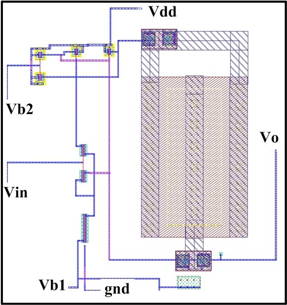
126 Figure 6.17: XOR2: schematic (left) and layout (right). Figure 6.18: Delay cell: schematic (left) and layout (right). 109

.")

127 Figure 6.19: Clocked-comparator: schematic (left) and layout (right). Figure 6.20: Non-clocked-comparator: schematic (left) and layout (right). 110

.")
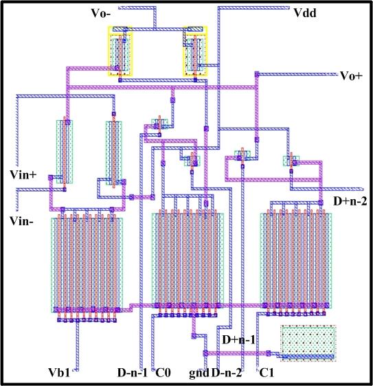
128 Figure 6.21: Adaptive engine: schematic (left) and layout (right). Figure 6.22: DFE core: schematic (left) and layout (right). 111

129 Figure 6.23: Layout of maximum-jitter adaptive DFE. 112
To learn fundamentals of high speed I/O link equalization techniques.
 1 ECEN 720 High-Speed Links: Circuits and Systems Lab5 Equalization Circuits Objective To learn fundamentals of high speed I/O link equalization techniques. Introduction An ideal cable could propagate
A 5-Gb/s 156-mW Transceiver with FFE/Analog Equalizer in 90-nm CMOS Technology Wang Xinghua a, Wang Zhengchen b, Gui Xiaoyan c,
 4th International Conference on Computer, Mechatronics, Control and Electronic Engineering (ICCMCEE 2015) A 5-Gb/s 156-mW Transceiver with FFE/Analog Equalizer in 90-nm CMOS Technology Wang Xinghua a,
ECEN689: Special Topics in High-Speed Links Circuits and Systems Spring 2012
 ECEN689: Special Topics in High-Speed Links Circuits and Systems Spring 0 Lecture 8: RX FIR, CTLE, & DFE Equalization Sam Palermo Analog & Mixed-Signal Center Texas A&M University Announcements Exam is
ECEN720: High-Speed Links Circuits and Systems Spring 2017
 ECEN720: High-Speed Links Circuits and Systems Spring 207 Lecture 8: RX FIR, CTLE, DFE, & Adaptive Eq. Sam Palermo Analog & Mixed-Signal Center Texas A&M University Announcements Lab 4 Report and Prelab
A10-Gb/slow-power adaptive continuous-time linear equalizer using asynchronous under-sampling histogram
 LETTER IEICE Electronics Express, Vol.10, No.4, 1 8 A10-Gb/slow-power adaptive continuous-time linear equalizer using asynchronous under-sampling histogram Wang-Soo Kim and Woo-Young Choi a) Department
Studies on FIR Filter Pre-Emphasis for High-Speed Backplane Data Transmission
 Studies on FIR Filter Pre-Emphasis for High-Speed Backplane Data Transmission Miao Li Department of Electronics Carleton University Ottawa, ON. K1S5B6, Canada Tel: 613 525754 Email:mili@doe.carleton.ca
A 10Gbps Analog Adaptive Equalizer and Pulse Shaping Circuit for Backplane Interface
 Proceedings of the 5th WSEAS Int. Conf. on CIRCUITS, SYSTEMS, ELECTRONICS, CONTROL & SIGNAL PROCESSING, Dallas, USA, November 1-3, 2006 225 A 10Gbps Analog Adaptive Equalizer and Pulse Shaping Circuit
EQUALIZERS. HOW DO? BY: ANKIT JAIN
 EQUALIZERS. HOW DO? BY: ANKIT JAIN AGENDA DFE (Decision Feedback Equalizer) Basics FFE (Feed-Forward Equalizer) Basics CTLE (Continuous-Time Linear Equalizer) Basics More Complex Equalization UNDERSTANDING
LSI and Circuit Technologies for the SX-8 Supercomputer
 LSI and Circuit Technologies for the SX-8 Supercomputer By Jun INASAKA,* Toshio TANAHASHI,* Hideaki KOBAYASHI,* Toshihiro KATOH,* Mikihiro KAJITA* and Naoya NAKAYAMA This paper describes the LSI and circuit
High-Speed Circuits and Systems Laboratory B.M.Yu. High-Speed Circuits and Systems Lab.
 High-Speed Circuits and Systems Laboratory B.M.Yu 1 Content 1. Introduction 2. Pre-emphasis 1. Amplitude pre-emphasis 2. Phase pre-emphasis 3. Circuit implantation 4. Result 5. Conclusion 2 Introduction
High Speed I/O 2-PAM Receiver Design. EE215E Project. Signaling and Synchronization. Submitted By
 High Speed I/O 2-PAM Receiver Design EE215E Project Signaling and Synchronization Submitted By Amrutha Iyer Kalpana Manickavasagam Pritika Dandriyal Joseph P Mathew Problem Statement To Design a high speed
A 0.18µm CMOS Gb/s Digitally Controlled Adaptive Line Equalizer with Feed-Forward Swing Control for Backplane Serial Link
 1 A 0.18µm CMOS 3.125-Gb/s Digitally Controlled Adaptive Line Equalizer with Feed-Forward Swing Control for Backplane Serial Link Ki-Hyuk Lee, Jae-Wook Lee nonmembers and Woo-Young Choi regular member
5Gbps Serial Link Transmitter with Pre-emphasis
 Gbps Serial Link Transmitter with Pre-emphasis Chih-Hsien Lin, Chung-Hong Wang and Shyh-Jye Jou Department of Electrical Engineering,National Central University,Chung-Li, Taiwan R.O.C. Abstract- High-speed
High-speed Serial Interface
 High-speed Serial Interface Lect. 9 Noises 1 Block diagram Where are we today? Serializer Tx Driver Channel Rx Equalizer Sampler Deserializer PLL Clock Recovery Tx Rx 2 Sampling in Rx Interface applications
CLOCK AND DATA RECOVERY (CDR) circuits incorporating
 circuits incorporating") IEEE JOURNAL OF SOLID-STATE CIRCUITS, VOL. 39, NO. 9, SEPTEMBER 2004 1571 Brief Papers Analysis and Modeling of Bang-Bang Clock and Data Recovery Circuits Jri Lee, Member, IEEE, Kenneth S. Kundert, and
IEEE JOURNAL OF SOLID-STATE CIRCUITS, VOL. 39, NO. 9, SEPTEMBER 2004 1571 Brief Papers Analysis and Modeling of Bang-Bang Clock and Data Recovery Circuits Jri Lee, Member, IEEE, Kenneth S. Kundert, and
EE290C Spring Lecture 5: Equalization Techniques. Elad Alon Dept. of EECS 9" FR4 26" FR4. 9" FR4, via stub.
 EE29C Spring 211 Lecture 5: Equalization Techniques Elad Alon Dept. of EECS Link Channels Attenuation [db] -1-2 -3-4 -5 9" FR4, via stub 9" FR4 26" FR4-6 26" FR4, via stub 2 4 6 8 1 frequency [GHz] EE29C
On Chip Active Decoupling Capacitors for Supply Noise Reduction for Power Gating and Dynamic Dual Vdd Circuits in Digital VLSI
 ELEN 689 606 Techniques for Layout Synthesis and Simulation in EDA Project Report On Chip Active Decoupling Capacitors for Supply Noise Reduction for Power Gating and Dynamic Dual Vdd Circuits in Digital
Ultra-high-speed Interconnect Technology for Processor Communication
 Ultra-high-speed Interconnect Technology for Processor Communication Yoshiyasu Doi Samir Parikh Yuki Ogata Yoichi Koyanagi In order to improve the performance of storage systems and servers that make up
DESIGN OF MULTI-BIT DELTA-SIGMA A/D CONVERTERS
 DESIGN OF MULTI-BIT DELTA-SIGMA A/D CONVERTERS DESIGN OF MULTI-BIT DELTA-SIGMA A/D CONVERTERS by Yves Geerts Alcatel Microelectronics, Belgium Michiel Steyaert KU Leuven, Belgium and Willy Sansen KU Leuven,
Tuesday, March 22nd, 9:15 11:00
 Nonlinearity it and mismatch Tuesday, March 22nd, 9:15 11:00 Snorre Aunet (sa@ifi.uio.no) Nanoelectronics group Department of Informatics University of Oslo Last time and today, Tuesday 22nd of March:
High-Speed Interconnect Technology for Servers
 High-Speed Interconnect Technology for Servers Hiroyuki Adachi Jun Yamada Yasushi Mizutani We are developing high-speed interconnect technology for servers to meet customers needs for transmitting huge
Delft University of Technology Faculty of Electrical Engineering, Mathematics and Computer Science
 Delft University of Technology Faculty of Electrical Engineering, Mathematics and Computer Science Analysis and Design of Decision Feedback Equalizers for bitrates of 10Gbps and Beyond in Submicron CMOS
Low-Voltage Wide Linear Range Tunable Operational Transconductance Amplifier
 Low-Voltage Wide Linear Range Tunable Operational Transconductance Amplifier A dissertation submitted in partial fulfillment of the requirement for the award of degree of Master of Technology in VLSI Design
LSI and Circuit Technologies of the SX-9
 TANAHASHI Toshio, TSUCHIDA Junichi, MATSUZAWA Hajime NIWA Kenji, SATOH Tatsuo, KATAGIRI Masaru Abstract This paper outlines the LSI and circuit technologies of the SX-9 as well as their inspection technologies.
To learn statistical bit-error-rate (BER) simulation, BER link noise budgeting and using ADS to model high speed I/O link circuits
 simulation, BER link noise budgeting and using ADS to model high speed I/O link circuits") 1 ECEN 720 High-Speed Links: Circuits and Systems Lab6 Link Modeling with ADS Objective To learn statistical bit-error-rate (BER) simulation, BER link noise budgeting and using ADS to model high speed
1 ECEN 720 High-Speed Links: Circuits and Systems Lab6 Link Modeling with ADS Objective To learn statistical bit-error-rate (BER) simulation, BER link noise budgeting and using ADS to model high speed
CHAPTER 4 ULTRA WIDE BAND LOW NOISE AMPLIFIER DESIGN
 93 CHAPTER 4 ULTRA WIDE BAND LOW NOISE AMPLIFIER DESIGN 4.1 INTRODUCTION Ultra Wide Band (UWB) system is capable of transmitting data over a wide spectrum of frequency bands with low power and high data
Source Coding and Pre-emphasis for Double-Edged Pulse width Modulation Serial Communication
 Source Coding and Pre-emphasis for Double-Edged Pulse width Modulation Serial Communication Abstract: Double-edged pulse width modulation (DPWM) is less sensitive to frequency-dependent losses in electrical
High-Speed Link Tuning Using Signal Conditioning Circuitry in Stratix V Transceivers
 High-Speed Link Tuning Using Signal Conditioning Circuitry in Stratix V Transceivers AN678 Subscribe This application note provides a set of guidelines to run error free across backplanes at high-speed
An 8-Gb/s Inductorless Adaptive Passive Equalizer in µm CMOS Technology
 JOURNAL OF SEMICONDUCTOR TECHNOLOGY AND SCIENCE, VOL.12, NO.4, DECEMBER, 2012 http://dx.doi.org/10.5573/jsts.2012.12.4.405 An 8-Gb/s Inductorless Adaptive Passive Equalizer in 0.18- µm CMOS Technology
A PROGRAMMABLE PRE-CURSOR ISI EQUALIZATION CIRCUIT FOR HIGH-SPEED SERIAL LINK OVER HIGHLY LOSSY BACKPLANE CHANNEL
 A PROGRAMMABLE PRE-CUROR II EQUALIZATION CIRCUIT FOR HIGH-PEED ERIAL LINK OVER HIGHLY LOY BACKPLANE CHANNEL Bo Wang, Dianyong Chen, Bangli Liang, Jinguang Jiang 2 and Tad Kwasniewski DOE, Carleton University,
06-011r0 Towards a SAS-2 Physical Layer Specification. Kevin Witt 11/30/2005
 06-011r0 Towards a SAS-2 Physical Layer Specification Kevin Witt 11/30/2005 Physical Layer Working Group Goal Draft a Specification which will: 1. Meet the System Designers application requirements, 2.
METHODOLOGY FOR THE DIGITAL CALIBRATION OF ANALOG CIRCUITS AND SYSTEMS
 METHODOLOGY FOR THE DIGITAL CALIBRATION OF ANALOG CIRCUITS AND SYSTEMS METHODOLOGY FOR THE DIGITAL CALIBRATION OF ANALOG CIRCUITS AND SYSTEMS with Case Studies by Marc Pastre Ecole Polytechnique Fédérale
ISSCC 2003 / SESSION 20 / WIRELESS LOCAL AREA NETWORKING / PAPER 20.5
 ISSCC 2003 / SESSION 20 / WIRELESS LOCAL AREA NETWORKING / PAPER 20.5 20.5 A 2.4GHz CMOS Transceiver and Baseband Processor Chipset for 802.11b Wireless LAN Application George Chien, Weishi Feng, Yungping
56+ Gb/s Serial Transmission using Duobinary Signaling
 56+ Gb/s Serial Transmission using Duobinary Signaling Jan De Geest Senior Staff R&D Signal Integrity Engineer, FCI Timothy De Keulenaer Doctoral Researcher, Ghent University, INTEC-IMEC Introduction Motivation
SHF Communication Technologies AG. Wilhelm-von-Siemens-Str. 23D Berlin Germany. Phone Fax
 SHF Communication Technologies AG -- Wilhelm-von-Siemens-Str. 23D 12277 Berlin Germany Phone +49 30 772051-0 Fax ++49 30 7531078 E-Mail: sales@shf.de Web: http://www.shf.de Datasheet SHF 12125 B Compact
if the conductance is set to zero, the equation can be written as following t 2 (4)
") 1 ECEN 720 High-Speed Links: Circuits and Systems Lab1 - Transmission Lines Objective To learn about transmission lines and time-domain reflectometer (TDR). Introduction Wires are used to transmit clocks
1 ECEN 720 High-Speed Links: Circuits and Systems Lab1 - Transmission Lines Objective To learn about transmission lines and time-domain reflectometer (TDR). Introduction Wires are used to transmit clocks
Delay-based clock generator with edge transmission and reset
 LETTER IEICE Electronics Express, Vol.11, No.15, 1 8 Delay-based clock generator with edge transmission and reset Hyunsun Mo and Daejeong Kim a) Department of Electronics Engineering, Graduate School,
100 Gb/s: The High Speed Connectivity Race is On
 100 Gb/s: The High Speed Connectivity Race is On Cathy Liu SerDes Architect, LSI Corporation Harold Gomard SerDes Product Manager, LSI Corporation October 6, 2010 Agenda 100 Gb/s Ethernet evolution SoC
IN HIGH-SPEED wireline transceivers, a (DFE) is often
 is often") 326 IEEE TRANSACTIONS ON CIRCUITS AND SYSTEMS II: EXPRESS BRIEFS, VOL. 59, NO. 6, JUNE 2012 Decision Feedback Equalizer Architectures With Multiple Continuous-Time Infinite Impulse Response Filters Shayan
326 IEEE TRANSACTIONS ON CIRCUITS AND SYSTEMS II: EXPRESS BRIEFS, VOL. 59, NO. 6, JUNE 2012 Decision Feedback Equalizer Architectures With Multiple Continuous-Time Infinite Impulse Response Filters Shayan
ALTHOUGH zero-if and low-if architectures have been
 IEEE JOURNAL OF SOLID-STATE CIRCUITS, VOL. 40, NO. 6, JUNE 2005 1249 A 110-MHz 84-dB CMOS Programmable Gain Amplifier With Integrated RSSI Function Chun-Pang Wu and Hen-Wai Tsao Abstract This paper describes
SINGLE-ENDED 16x8 GBPS DATA BUS IN 90NM CMOS
 SINGLE-ENDED 16x8 GBPS DATA BUS IN 90NM CMOS By SAURABH MANDHANYA A thesis submitted in partial fulfillment of the requirements for the degree of MASTER OF SCIENCE IN ELECTRICAL ENGINEERING WASHINGTON
Highly linear common-gate mixer employing intrinsic second and third order distortion cancellation
 Highly linear common-gate mixer employing intrinsic second and third order distortion cancellation Mahdi Parvizi a), and Abdolreza Nabavi b) Microelectronics Laboratory, Tarbiat Modares University, Tehran
OIF CEI 6G LR OVERVIEW
 OIF CEI 6G LR OVERVIEW Graeme Boyd, Yuriy Greshishchev T10 SAS-2 WG meeting, Houston, 25-26 May 2005 www.pmc-sierra.com 1 Outline! Why CEI-6G LR is of Interest to SAS-2?! CEI-6G- LR Specification Methodology!
A 5-8 Gb/s Low-Power Transmitter with 2-Tap Pre-Emphasis Based on Toggling Serialization
 A 5-8 Gb/s Low-Power Transmitter with 2-Tap Pre-Emphasis Based on Toggling Serialization Sung-Geun Kim, Tongsung Kim, Dae-Hyun Kwon, and Woo-Young Choi Department of Electrical and Electronic Engineering,
Tuesday, March 29th, 9:15 11:30
 Oscillators, Phase Locked Loops Tuesday, March 29th, 9:15 11:30 Snorre Aunet (sa@ifi.uio.no) Nanoelectronics group Department of Informatics University of Oslo Last time and today, Tuesday 29th of March:
SOLIMAN A. MAHMOUD Department of Electrical Engineering, Faculty of Engineering, Cairo University, Fayoum, Egypt
 Journal of Circuits, Systems, and Computers Vol. 14, No. 4 (2005) 667 684 c World Scientific Publishing Company DIGITALLY CONTROLLED CMOS BALANCED OUTPUT TRANSCONDUCTOR AND APPLICATION TO VARIABLE GAIN
ISSCC 2004 / SESSION 26 / OPTICAL AND FAST I/O / 26.8
 ISSCC 2004 / SESSION 26 / OPTICAL AND FAST I/O / 26.8 26.8 A 2GHz CMOS Variable-Gain Amplifier with 50dB Linear-in-Magnitude Controlled Gain Range for 10GBase-LX4 Ethernet Chia-Hsin Wu, Chang-Shun Liu,
Ensuring Signal and Power Integrity for High-Speed Digital Systems
 Ensuring Signal and Power Integrity for High-Speed Digital Systems An EMC Perspective Christian Schuster Institut für Theoretische Elektrotechnik Technische Universität Hamburg-Harburg (TUHH) Invited Presentation
To learn S-parameters, eye diagram, ISI, modulation techniques and their simulations in MATLAB and Cadence.
 1 ECEN 720 High-Speed Links: Circuits and Systems Lab2- Channel Models Objective To learn S-parameters, eye diagram, ISI, modulation techniques and their simulations in MATLAB and Cadence. Introduction
Advanced Operational Amplifiers
 IsLab Analog Integrated Circuit Design OPA2-47 Advanced Operational Amplifiers כ Kyungpook National University IsLab Analog Integrated Circuit Design OPA2-1 Advanced Current Mirrors and Opamps Two-stage
Chapter 5. Operational Amplifiers and Source Followers. 5.1 Operational Amplifier
 Chapter 5 Operational Amplifiers and Source Followers 5.1 Operational Amplifier In single ended operation the output is measured with respect to a fixed potential, usually ground, whereas in double-ended
Comparison of Time Domain and Statistical IBIS-AMI Analyses Mike LaBonte SiSoft
 Comparison of Time Domain and Statistical IBIS-AMI Analyses Mike LaBonte SiSoft Asian IBIS Summit 2017 Taipei, ROC November 15, 2017 9 Combinations of TX and RX Model Types AMI file has: GetWave_Exists
Comparison of Time Domain and Statistical IBIS-AMI Analyses
 Comparison of Time Domain and Statistical IBIS-AMI Analyses Mike LaBonte SiSoft Asian IBIS Summit 2017 Shanghai, PRC November 13, 2017 9 Combinations of TX and RX Model Types AMI file has: GetWave_Exists
A 10-Gb/s Multiphase Clock and Data Recovery Circuit with a Rotational Bang-Bang Phase Detector
 JOURNAL OF SEMICONDUCTOR TECHNOLOGY AND SCIENCE, VOL.16, NO.3, JUNE, 2016 ISSN(Print) 1598-1657 http://dx.doi.org/10.5573/jsts.2016.16.3.287 ISSN(Online) 2233-4866 A 10-Gb/s Multiphase Clock and Data Recovery
ECEN720: High-Speed Links Circuits and Systems Spring 2017
 ECEN72: High-Speed Links Circuits and Systems Spring 217 Lecture 4: Channel Pulse Model & Modulation Schemes Sam Palermo Analog & Mixed-Signal Center Texas A&M University Announcements & Agenda Lab 1 Report
A 10Gb/s 10mm On-Chip Serial Link in 65nm CMOS Featuring a Half-Rate Time-Based Decision Feedback Equalizer
 A 10Gb/s 10mm On-Chip Serial Link in 65nm CMOS Featuring a Half-Rate Time-Based Decision Feedback Equalizer Po-Wei Chiu, Somnath Kundu, Qianying Tang, and Chris H. Kim University of Minnesota, Minneapolis,
HIGH-SPEED LOW-POWER ON-CHIP GLOBAL SIGNALING DESIGN OVERVIEW. Xi Chen, John Wilson, John Poulton, Rizwan Bashirullah, Tom Gray
 HIGH-SPEED LOW-POWER ON-CHIP GLOBAL SIGNALING DESIGN OVERVIEW Xi Chen, John Wilson, John Poulton, Rizwan Bashirullah, Tom Gray Agenda Problems of On-chip Global Signaling Channel Design Considerations
This chapter discusses the design issues related to the CDR architectures. The
 Chapter 2 Clock and Data Recovery Architectures 2.1 Principle of Operation This chapter discusses the design issues related to the CDR architectures. The bang-bang CDR architectures have recently found
A 24Gb/s Software Programmable Multi-Channel Transmitter
 A 24Gb/s Software Programmable Multi-Channel Transmitter A. Amirkhany 1, A. Abbasfar 2, J. Savoj 2, M. Jeeradit 2, B. Garlepp 2, V. Stojanovic 2,3, M. Horowitz 1,2 1 Stanford University 2 Rambus Inc 3
EL4089 and EL4390 DC Restored Video Amplifier
 EL4089 and EL4390 DC Restored Video Amplifier Application Note AN1089.1 Authors: John Lidgey, Chris Toumazou and Mike Wong The EL4089 is a complete monolithic video amplifier subsystem in a single 8-pin
THE TREND toward implementing systems with low
 724 IEEE JOURNAL OF SOLID-STATE CIRCUITS, VOL. 30, NO. 7, JULY 1995 Design of a 100-MHz 10-mW 3-V Sample-and-Hold Amplifier in Digital Bipolar Technology Behzad Razavi, Member, IEEE Abstract This paper
EE301 Electronics I , Fall
 EE301 Electronics I 2018-2019, Fall 1. Introduction to Microelectronics (1 Week/3 Hrs.) Introduction, Historical Background, Basic Consepts 2. Rewiev of Semiconductors (1 Week/3 Hrs.) Semiconductor materials
Microcircuit Electrical Issues
 Microcircuit Electrical Issues Distortion The frequency at which transmitted power has dropped to 50 percent of the injected power is called the "3 db" point and is used to define the bandwidth of the
DESIGN CONSIDERATIONS AND PERFORMANCE REQUIREMENTS FOR HIGH SPEED DRIVER AMPLIFIERS. Nils Nazoa, Consultant Engineer LA Techniques Ltd
 DESIGN CONSIDERATIONS AND PERFORMANCE REQUIREMENTS FOR HIGH SPEED DRIVER AMPLIFIERS Nils Nazoa, Consultant Engineer LA Techniques Ltd 1. INTRODUCTION The requirements for high speed driver amplifiers present
Chapter 13 Oscillators and Data Converters
 Chapter 13 Oscillators and Data Converters 13.1 General Considerations 13.2 Ring Oscillators 13.3 LC Oscillators 13.4 Phase Shift Oscillator 13.5 Wien-Bridge Oscillator 13.6 Crystal Oscillators 13.7 Chapter
SV2C 28 Gbps, 8 Lane SerDes Tester
 SV2C 28 Gbps, 8 Lane SerDes Tester Data Sheet SV2C Personalized SerDes Tester Data Sheet Revision: 1.0 2015-03-19 Revision Revision History Date 1.0 Document release. March 19, 2015 The information in
Backchannel Modeling and Simulation Using Recent Enhancements to the IBIS Standard
 Backchannel Modeling and Simulation Using Recent Enhancements to the IBIS Standard By Ken Willis, Product Engineering Architect; Ambrish Varma, Senior Principal Software Engineer; Dr. Kumar Keshavan, Senior
Increasing Performance Requirements and Tightening Cost Constraints
 Maxim > Design Support > Technical Documents > Application Notes > Power-Supply Circuits > APP 3767 Keywords: Intel, AMD, CPU, current balancing, voltage positioning APPLICATION NOTE 3767 Meeting the Challenges
To learn Statistical Bit-error-rate (BER) simulation, BERlink noise budgeting and usage of ADS to model high speed I/O link circuits.
 simulation, BERlink noise budgeting and usage of ADS to model high speed I/O link circuits.") 1 ECEN 720 High-Speed Links Circuits and Systems Lab6 Link Modeling with ADS Objective To learn Statistical Bit-error-rate (BER) simulation, BERlink noise budgeting and usage of ADS to model high speed
1 ECEN 720 High-Speed Links Circuits and Systems Lab6 Link Modeling with ADS Objective To learn Statistical Bit-error-rate (BER) simulation, BERlink noise budgeting and usage of ADS to model high speed
Module 12 : System Degradation and Power Penalty
 Module 12 : System Degradation and Power Penalty Lecture : System Degradation and Power Penalty Objectives In this lecture you will learn the following Degradation during Propagation Modal Noise Dispersion
ISSCC 2004 / SESSION 26 / OPTICAL AND FAST I/O / 26.6
 ISSCC 2004 / SESSION 26 / OPTICAL AND FAST I/O / 26.6 26.6 40Gb/s Amplifier and ESD Protection Circuit in 0.18µm CMOS Technology Sherif Galal, Behzad Razavi University of California, Los Angeles, CA Optical
INVENTION DISCLOSURE- ELECTRONICS SUBJECT MATTER IMPEDANCE MATCHING ANTENNA-INTEGRATED HIGH-EFFICIENCY ENERGY HARVESTING CIRCUIT
 INVENTION DISCLOSURE- ELECTRONICS SUBJECT MATTER IMPEDANCE MATCHING ANTENNA-INTEGRATED HIGH-EFFICIENCY ENERGY HARVESTING CIRCUIT ABSTRACT: This paper describes the design of a high-efficiency energy harvesting
Jitter in Digital Communication Systems, Part 1
 Application Note: HFAN-4.0.3 Rev.; 04/08 Jitter in Digital Communication Systems, Part [Some parts of this application note first appeared in Electronic Engineering Times on August 27, 200, Issue 8.] AVAILABLE
Low Jitter, Low Emission Timing Solutions For High Speed Digital Systems. A Design Methodology
 Low Jitter, Low Emission Timing Solutions For High Speed Digital Systems A Design Methodology The Challenges of High Speed Digital Clock Design In high speed applications, the faster the signal moves through
Equalize 10Gbase-CX4 and Copper InfiniBand Links with the MAX3983
 Design Note: HFDN-27.0 Rev.1; 04/08 Equalize 10Gbase-CX4 and Copper InfiniBand Links with the MAX3983 AAILABLE Equalize 10Gbase-CX4 and Copper InfiniBand Links with the MAX3983 1 Introduction This discussion
CHAPTER 6 PHASE LOCKED LOOP ARCHITECTURE FOR ADC
 138 CHAPTER 6 PHASE LOCKED LOOP ARCHITECTURE FOR ADC 6.1 INTRODUCTION The Clock generator is a circuit that produces the timing or the clock signal for the operation in sequential circuits. The circuit
Design of Analog CMOS Integrated Circuits
 Design of Analog CMOS Integrated Circuits Behzad Razavi Professor of Electrical Engineering University of California, Los Angeles H Boston Burr Ridge, IL Dubuque, IA Madison, WI New York San Francisco
About the Tutorial. Audience. Prerequisites. Copyright & Disclaimer. Linear Integrated Circuits Applications
 About the Tutorial Linear Integrated Circuits are solid state analog devices that can operate over a continuous range of input signals. Theoretically, they are characterized by an infinite number of operating
Channel operating margin for PAM4 CDAUI-8 chip-to-chip interfaces
 Channel operating margin for PAM4 CDAUI-8 chip-to-chip interfaces Adam Healey Avago Technologies IEEE P802.3bs 400 GbE Task Force March 2015 Introduction Channel Operating Margin (COM) is a figure of merit
A 3-10GHz Ultra-Wideband Pulser
 A 3-10GHz Ultra-Wideband Pulser Jan M. Rabaey Simone Gambini Davide Guermandi Electrical Engineering and Computer Sciences University of California at Berkeley Technical Report No. UCB/EECS-2006-136 http://www.eecs.berkeley.edu/pubs/techrpts/2006/eecs-2006-136.html
1-13GHz Wideband LNA utilizing a Transformer as a Compact Inter-stage Network in 65nm CMOS
 -3GHz Wideband LNA utilizing a Transformer as a Compact Inter-stage Network in 65nm CMOS Hyohyun Nam and Jung-Dong Park a Division of Electronics and Electrical Engineering, Dongguk University, Seoul E-mail
Lecture 11: Clocking
 High Speed CMOS VLSI Design Lecture 11: Clocking (c) 1997 David Harris 1.0 Introduction We have seen that generating and distributing clocks with little skew is essential to high speed circuit design.
Serial Data Transmission
 Serial Data Transmission Dr. José Ernesto Rayas Sánchez 1 Outline Baseband serial transmission Line Codes Bandwidth of serial data streams Block codes Serialization Intersymbol Interference (ISI) Jitter
High Speed Digital Systems Require Advanced Probing Techniques for Logic Analyzer Debug
 JEDEX 2003 Memory Futures (Track 2) High Speed Digital Systems Require Advanced Probing Techniques for Logic Analyzer Debug Brock J. LaMeres Agilent Technologies Abstract Digital systems are turning out
NEW WIRELESS applications are emerging where
 IEEE JOURNAL OF SOLID-STATE CIRCUITS, VOL. 39, NO. 4, APRIL 2004 709 A Multiply-by-3 Coupled-Ring Oscillator for Low-Power Frequency Synthesis Shwetabh Verma, Member, IEEE, Junfeng Xu, and Thomas H. Lee,
DDR4 memory interface: Solving PCB design challenges
 DDR4 memory interface: Solving PCB design challenges Chang Fei Yee - July 23, 2014 Introduction DDR SDRAM technology has reached its 4th generation. The DDR4 SDRAM interface achieves a maximum data rate
ECEN 720 High-Speed Links: Circuits and Systems
 1 ECEN 720 High-Speed Links: Circuits and Systems Lab4 Receiver Circuits Objective To learn fundamentals of receiver circuits. Introduction Receivers are used to recover the data stream transmitted by
A 1.5 Gbps Transceiver Chipset in 0.13-mm CMOS for Serial Digital Interface
 JOURNAL OF SEMICONDUCTOR TECHNOLOGY AND SCIENCE, VOL.17, NO.4, AUGUST, 2017 ISSN(Print) 1598-1657 https://doi.org/10.5573/jsts.2017.17.4.552 ISSN(Online) 2233-4866 A 1.5 Gbps Transceiver Chipset in 0.13-mm
To learn S-parameter, eye diagram, ISI, modulation techniques and to simulate in Matlab and Cadence.
 1 ECEN 689 High-Speed Links Circuits and Systems Lab2- Channel Models Objective To learn S-parameter, eye diagram, ISI, modulation techniques and to simulate in Matlab and Cadence. Introduction S-parameters
ISSCC 2003 / SESSION 10 / HIGH SPEED BUILDING BLOCKS / PAPER 10.8
 ISSCC 2003 / SESSION 10 / HIGH SPEED BUILDING BLOCKS / PAPER 10.8 10.8 10Gb/s Limiting Amplifier and Laser/Modulator Driver in 0.18µm CMOS Technology Sherif Galal, Behzad Razavi Electrical Engineering
Plastic straw: future of high-speed signaling
 Supplementary Information for Plastic straw: future of high-speed signaling Ha Il Song, Huxian Jin, and Hyeon-Min Bae * Korea Advanced Institute of Science and Technology (KAIST), Department of Electrical
Adaptive Receivers for High-Speed Wireline Links. Dustin Dunwell
 Adaptive Receivers for High-Speed Wireline Links by Dustin Dunwell A thesis submitted in conformity with the requirements for the degree of Doctor of Philosophy Graduate Department of Electrical and Computer
Design Of A Comparator For Pipelined A/D Converter
 Design Of A Comparator For Pipelined A/D Converter Ms. Supriya Ganvir, Mr. Sheetesh Sad ABSTRACT`- This project reveals the design of a comparator for pipeline ADC. These comparator is designed using preamplifier
Validation & Analysis of Complex Serial Bus Link Models
 Validation & Analysis of Complex Serial Bus Link Models Version 1.0 John Pickerd, Tektronix, Inc John.J.Pickerd@Tek.com 503-627-5122 Kan Tan, Tektronix, Inc Kan.Tan@Tektronix.com 503-627-2049 Abstract
DESIGN OF LOW-VOLTAGE WIDE TUNING RANGE CMOS MULTIPASS VOLTAGE-CONTROLLED RING OSCILLATOR
 DESIGN OF LOW-VOLTAGE WIDE TUNING RANGE CMOS MULTIPASS VOLTAGE-CONTROLLED RING OSCILLATOR by Jie Ren Submitted in partial fulfilment of the requirements for the degree of Master of Applied Science at Dalhousie
Engineering the Power Delivery Network
 C HAPTER 1 Engineering the Power Delivery Network 1.1 What Is the Power Delivery Network (PDN) and Why Should I Care? The power delivery network consists of all the interconnects in the power supply path
ECEN 720 High-Speed Links Circuits and Systems
 1 ECEN 720 High-Speed Links Circuits and Systems Lab4 Receiver Circuits Objective To learn fundamentals of receiver circuits. Introduction Receivers are used to recover the data stream transmitted by transmitters.
ECEN 474/704 Lab 6: Differential Pairs
 ECEN 474/704 Lab 6: Differential Pairs Objective Design, simulate and layout various differential pairs used in different types of differential amplifiers such as operational transconductance amplifiers
VERIFICATION OF RECEIVER EQUALIZATION BY INTEGRATING DATAFLOW SIMULATION AND PHYSICAL CHANNELS. A Thesis. presented to.
 VERIFICATION OF RECEIVER EQUALIZATION BY INTEGRATING DATAFLOW SIMULATION AND PHYSICAL CHANNELS A Thesis presented to the Faculty of California Polytechnic State University, San Luis Obispo In Partial Fulfillment
RiseUp RU8-DP-DV Series 19mm Stack Height Final Inch Designs in Serial ATA Generation 1 Applications. Revision Date: March 18, 2005
 RiseUp RU8-DP-DV Series 19mm Stack Height Final Inch Designs in Serial ATA Generation 1 Applications Revision Date: March 18, 2005 Copyrights and Trademarks Copyright 2005 Samtec, Inc. Developed in conjunction