35-45 giga hertz transceiver system for phase and magnitude detection
|
|
|
- Joseph Lambert
- 6 years ago
- Views:
Transcription

. Masters Theses. 4552. edu/masters_theses/4552 This Thesis - Open Access is brought to you for free and open access by Scholars' Mine.")
1 Scholars' Mine Masters Theses Student Research & Creative Works Summer giga hertz transceiver system for phase and magnitude detection Aman Aflaki Beni Follow this and additional works at: Part of the Electrical and Computer Engineering Commons Department: Recommended Citation Aflaki Beni, Aman, "35-45 giga hertz transceiver system for phase and magnitude detection" (2007). Masters Theses This Thesis - Open Access is brought to you for free and open access by Scholars' Mine. It has been accepted for inclusion in Masters Theses by an authorized administrator of Scholars' Mine. This work is protected by U. S. Copyright Law. Unauthorized use including reproduction for redistribution requires the permission of the copyright holder. For more information, please contact scholarsmine@mst.edu.
2
3 35-45 GIGA HERTZ TRANSCEIVER SYSTEM FOR PHASE AND MAGNITUDE DETECTION by AMAN AFLAKI BENI A THESIS Presented to the Faculty of the Graduate School of the UNIVERSITY OF MISSOURI-ROLLA In Partial Fulfillment of the Requirements for the Degree MASTER OF SCIENCE IN ELECTRICAL ENGINEERING 2007 Approved by D. J. POMMERENKE, Co-advisor R. ZOUGHI, Co-advisor J. L. DREWNIAK
4 ii 2007 Aman Aflaki Beni All Rights Reserved
5 iii ABSTRACT Nondestructive evaluation (NDE) is the science and practice of examining an object in a way that the object s usefulness is not adversely affected. Different types of NDE methods exist but this thesis is based on microwave and millimeter wave NDE using imaging techniques. Microwave NDE is based on illuminating the object under test with a microwave signal and studying the various properties of the reflected signal from the object. This reflected signal contains some information about the inner structure of the object under test. This information may be contained in several parameters including the phase and magnitude of the reflected signal. The goal of this project is to design and build a Q-band coherent transceiver that is capable of measuring the reflected signal s phase and magnitude so that an image of the object under test may be reconstructed. From the several techniques that can be used to construct an image of the object under test, techniques of interest to this work include synthetic aperture focusing technique (SAFT) and microwave holography. The transceiver system should have the ability to sweep a large portion of Q-band frequency range in small frequency steps as quick as possible while the detected phase and magnitude of the reflected signal is very accurate. Several different designs were studied and the final schematic diagram of the transceiver system was determined. One of the most important modules that was designed, implemented and tested in the laboratory was an accurate phase/magnitude detector circuit. The compared results of the scans using the transceiver system and VNA showed that this transceiver system has a great potential to replace a VNA for the purpose of microwave and millimeter wave imaging.
6 iv ACKNOWLEDGMENTS First, I would like to offer my sincere gratitude to my advisors whom I owe more than I can adequately express here and definitely my special appreciation goes to them, to Dr. Pommerenke for his vital guidance and endless support throughout my research projects, and to Dr. Zoughi, who advised and helped me in many ways including correcting my thesis in different stages. Also, I would like to express my gratitude to Dr. Drewniak for serving on my committee. My special thanks go to Mr. Toby Case whose contribution were invaluable in the design, characterization and testing of the system. I also want to thank Mr. Tayeb Ghasr and Dr. Kharkovsky for their help in mechanically assembling the system and testing it. In addition, I would like to thank Lijun Han and Arnaud Ngassam who assisted in building the first version of the phase/magnitude detector board. I also would like to thank the rest of the fine people in Electromagnetic Compatibility Laboratory (EMC LAB) and Applied Microwave Nondestructive Testing Laboratory (amntl) for their help and all of the wonderful times. I would like to express my heartfelt appreciation to my parents for their love, guidance, support and trust. This project was funded by NASA Marshall Space Flight Center, under grant No. NNM06AA089.
7 v TABLE OF CONTENTS Page ABSTRACT...iii ACKNOWLEDGMENTS... iv LIST OF ILLUSTRATIONS...viii SECTION 1. INTRODUCTION NONDESTRUCTIVE EVALUATION MICROWAVE IMAGING SCANNING SYSTEM COMPONENTS TRANSCEIVER SYSTEM TRANSCEIVER DESIGN AND RELATED HARDWARE INTRODUCTION SYNTHESIZERS (TRANSMITTER AND RECEIVER) UP MIXER INCLUDING AN INTERNAL DOUBLER (TRANSMITTER) ISOLATOR (TRANSMITTER) DUAL-DIRECTIONAL COUPLER (TRANSMITTER) HORN ANTENNA (TRANSMITTER AND RECEIVER) DOWN MIXER INCLUDING AN INTERNAL DOUBLER (RECEIVER) DEGREE HYBRID DIRECTIONAL COUPLER (RECEIVER) POWER DIVIDER (RECEIVER) POWER SUPPLY BOARD PHASE/MAGNITUDE DETECTION BOARD INTRODUCTION FIRST APPROACH TO PHASE AND MAGNITUDE DETECTION SECOND APPROACH FOR PHASE MAGNITUDE DETECTION Low Noise Amplifiers Helical Filter Low-Pass Filter High-Pass Filter Voltage Variable Attenuator... 44
8 vi Power Splitter Delay Lines Comparison Between the Responses of the Two Channels Phase/Magnitude Detectors Absolute Magnitude Detectors PHASE/MAGNITUDE DETECTOR BOARD TESTS AND RESULTS INTRODUCTION PHASE DETECTION PROCESS ERROR SOURCES DYNAMIC RANGE CALCULATIONS SCANNING PROCEDURE AND RESULTS INTRODUCTION FIRST SCAN SETUP AND RESULTS SECOND SCAN SETUP SECOND SCAN RESULTS AND COMPARISON WITH VNA RESULTS SUMMARY AND FUTURE WORK SUMMARY FUTURE WORK APPENDICES A. CIRCUIT DIAGRAM OF THE PHASE MAGNITUDE DETECTOR BOARD AND DATASHEETS OF THE COMPONENTS THAT ARE USED IN THE TRANSCEIVER B. SIGNAL POWER LEVELS AND LEVEL DIAGRAMS IN THE PHASE/MAGNITUDE DETECTOR CIRCUIT C. SIGNAL POWER LEVELS AND LEVEL DIAGRAMS IN THE TRANSCEIVER SYSTEM D. CIRCUIT DIAGRAM OF THE POWER SUPPLY BOARD E. SYNTHESIZER S CHARACTERISTICS F. CIRCUIT DIAGRAM OF THE PHASE/MAGNITUDE DETECTOR BOARD. 107 G. TRANSCEIVER CALIBRATION DATA
9 vii H. SATURATION LEVELS IN PHASE MAGNITUDE DETECTOR BOARD I. CURRENT CONSUMPTION OF THE TRANSCEIVER SYSTEM J. DC WIRINGS AND CONNECTOR WIRE COLORS BIBLIOGRAPHY VITA
10 viii LIST OF ILLUSTRATIONS Figure 1.1 Illustration of raster scanning procedure Figure 1.2 Picture of the scanning system Figure 2.1 Block diagram of the transceiver system... 7 Figure 2.2 Synthesizer 1 output spectrum Figure 2.3 Synthesizer 1 output spectrum Figure 2.4 Synthesizer 1 output spectrum Figure 2.5 Synthesizer 2 output spectrum Figure 2.6 Synthesizer 2 output spectrum Figure 2.7 Block diagram of the up mixer Figure 2.8 Circuitry for biasing IF1 and IF Figure 2.9 XU1004 Mimix broadband s transmitter Figure 2.10 QIF-Q0000, a Q-band Isolator from Quinstar Tech, Inc Figure 2.11 QJD-Q , dual-directional coupler from Quinstar Technologies, Inc Figure 2.12 Dual-directional coupler Figure 2.13 ARH , rectangular horn antenna from WiseWave Technologies, Inc Figure 2.14 Block diagram of the down mixer Figure 2.15 XR1004 Mimix broadband s receiver Figure 2.16 Receiver module 1 output spectrum Figure 2.17 Receiver module 1 output spectrum Figure 2.18 Receiver module 1 output spectrum Figure degree hybrid from ATM Inc Figure 2.20 Schematic diagram of the 90-degree hybrid from ATM Inc Figure 2.21 Output of the receiver after the 90-degree hybrid Figure 2.22 Measurement setup to test the power divider Figure 2.23 S21 measurement between the input and one of theoutputs of the power divider Figure 2.24 TDR measurement between the input and one of theoutputs the power divider Figure 2.25 Circuit diagram of the power supply board for the RF Transceiver... 26
11 ix Figure 2.26 Layout of the power supply board for the RF transceiver Figure 3.1 Picture of the back-side of the phase/magnitude board Figure 3.2 Superheterodyne receiver architecture Figure 3.3 Block diagram of the phase/magnitude detector (first approach) Figure 3.4 Layout of the phase/magnitude detector in Protel DXP (first approach) Figure 3.5 Picture of the populated phase/magnitude detector (first approach) Figure 3.6 Holographic images of a ramp panel with implanted voids at Q-band for different phase errors Figure 3.7 Block diagram of the phase/magnitude detector (second approach) Figure 3.8 Picture of the unpopulated phase/magnitude detector board Figure 3.9 Picture of the populated phase/magnitude detector board Figure 3.10 Circuit diagram of HMC376LP3 block Figure 3.11 S21 measurement on HMC376LP3 using HP8753D VNA Figure 3.12 S21 measurement on two stages of HMC376LP3 using HP8753D VNA Figure 3.13 S21 measurement on the first helical filter on the RF channel using HP8753D VNA Figure 3.14 S21 measurement on the low-pass filter on the RF channel using HP8753D VNA Figure 3.15 S21 measurement on the high-pass filter on the RF channel using HP8753D VNA Figure 3.16 Circuit diagram if voltage variable attenuator block Figure 3.17 S21 measurement on voltage variable attenuator on the RF channel using HP8753D VNA Figure 3.18 Circuit diagram of the power splitter block Figure 3.19 Picture of the delay lines and power splitters Figure 3.20 Frequency response of the RF and reference channel between the input connector and one of the inputs of the phase/magnitude detector Figure 3.21 Block diagram of AD Figure 3.22 Detected magnitude output vs. the power ratio of the two inputs at 900 MHz Figure 3.23 Detected magnitude error vs. the power ratio of the two inputs at 900 MHz Figure 3.24 Detected output voltage of the phase detector vs. the phase difference of the two inputs Figure 3.25 Error voltage of the phase detector vs. the phase difference of the two inputs... 53
12 x Figure 3.26 Output voltage of the absolute magnitude detector vs. the input power at 900 MHz Figure 4.1 Test setup that was used to examine the phase/magnitude detector board Figure 4.2 Three phase outputs of the phase/magnitude detector board while the input phase difference is being changed Figure 4.3 Three phase outputs of the phase/magnitude detector board centred Figure 4.4 Test setup to check the stability of the phase/magnitude board Figure 4.5 Output phase voltage of the first detector for a constant input phase difference Figure 4.6 Test setup to check the phase accuracy of the signal generators Figure 4.7 Test setup to measure the phase detection accuracy of the phase/magnitude board Figure 4.8 Detected phase by phase/magnitude detector and VNA Figure 4.9 Phase/magnitude s detected phase error compared to the detected phase by VNA Figure 5.1 Picture of the scanning system Figure 5.2 Picture of the probe on the sample under test Figure 5.3 Images of the raw output voltages at GHz Figure 5.4 Picture of the scanning system Figure 5.5 Dual-directional coupler in the transceiver system Figure 5.6 Picture of the sample under test Figure 5.7 Picture of the probe on the sample under test Figure 5.8 Characterized single-value phase and magnitude images of the scan for 3 frequencies Figure 5.9 Picture of the open-ended waveguide above the sample under test in the VNA scan setup Figure 5.10 Comparison between the SAFT images focused on the second post from the left generated using the transceiver system and VNA at 45 GHz; the left column shows SAFT images using a VNA and the right column are images using the transceiver system Figure 5.11 Comparison between the SAFT images focused on the first post from the left generated using the transceiver system and VNA at 45 GHz; the left column shows SAFT images using a VNA and the right column are images using the transceiver system
13 1. INTRODUCTION 1.1. NONDESTRUCTIVE EVALUATION Nondestructive evaluation (NDE) describes the process of examining a material without altering its usefulness. NDE is the using a physical phenomenon to discover the quality and characteristics of an object under test. There are different types of NDE methods that are used for different applications. Some well-established NDE methods include liquid penetrant, ultrasound, magnetic particle testing, eddy current, acoustic emission and radiography [1]. Microwave and millimeter wave NDE are considered as emerging methods with great potential for inspecting a wide variety of materials [2]. In the next section, microwave imaging technique used for microwave NDE applications is briefly introduced MICROWAVE IMAGING Microwave imaging is based on transmitting a signal onto a material under test and receiving the reflected signal. Different information about the structure of the material can be extracted from the various properties of the reflected signal. Microwave and millimeter wave imaging techniques have shown great potential for generating images of various composite structures with high spatial-resolution [3]. Microwave signals can penetrate inside of dielectric materials and provide detailed information about their inner structure [4]. This information may be obtained from the phase and/or magnitude of the reflected signal. One of the microwave imaging methods, for generating high-resolution images of is the synthetic aperture focusing technique (SAFT). In SAFT, the data may be acquired using raster scanning. By Figure 1.1 shows the procedure of raster scanning. In raster scanning the probe is held at a certain distance above the material under test while it moves in the manner illustrated in Figure 1.1. This microwave probe can be a horn antenna or an open-ended waveguide. The acquired raster scan data is used as if a larger antenna is used. So, a larger antenna with a narrower beam is synthetically created from the data acquired using a small antenna that has scanned the material under test. The advantage of a larger antenna is having a narrower beam that can result in higher spatial resolution images. In principle, SAFT is based on phase
14 2 matching, while compensating for the delays associated with the different propagation distances [3]. SAFT can generate images with high spatial resolution but does not provide any depth resolution. To have information in depth which can result in a high-resolution 3 dimensional image, a narrow pulse must also be used [5]. Since generating a narrow pulse at microwave and millimeter wave frequencies is not easy, frequency sweeping is used instead. The time domain fourier transform of a sweep in frequency domain is a pulse. The wider the frequency sweep range, the narrower is the equivalent pulse and the narrower the pulse, the higher the depth resolution will be. The technique that combines SAFT and swept frequency techniques, resulting in high-resolution 3D images is referred to as microwave holography [5]. A defect which can be an impurity in the material under test can be detected by analyzing the reflected signal, using microwave and millimeter wave holography. After processing the data an image can be constructed providing defect information such as its position within the material, shape and size [6]. Y Material under test X Moving Probe Figure 1.1 Illustration of raster scanning procedure.
15 3 In this thesis, raster scanning is performed on a sample with a horn antenna or an open-ended waveguide as a probe, as shown in Figure 1.1. Data is acquired using a transceiver which gives the magnitude and phase of reflected signal referenced at the probe for every point in the raster scan. The step size or scanning increment between adjacent measurement points can vary between 1 mm to 4 mm depending on the required resolution. The transceiver is designed to operate at a frequency in the range of 35 to 45 GHz which covers a large portion of Q-band (33-50 GHz) SCANNING SYSTEM COMPONENTS For the purpose of this thesis, an already existing scanning platform, capable of performing raster scans was used, as shown in Figure 1.2. In this system the computer controls the position of the transceiver system which is attached to the scanner and acquires and saves the data for each scan position. PC including a DAQ card Power supply Motor controller Wireless USB Receiver Scanner motors Prepared sample Transceiver system Figure 1.2 Picture of the scanning system.
16 TRANSCEIVER SYSTEM Subsequent to determining the overall required design characteristics of the transceiver, its assembly and more importantly its testing commenced. The primary purpose of this work has been to design an accurate and robust transceiver operating in Q-band and capable of producing coherent reflected signal information. In this way, a Q- band vector network analyzer is essentially designed and constructed. Furthermore, the transceiver system can be mounted on a scanner directly while it is not possible to mount a VNA on a scanner. So, being accurate in determining phase and magnitude while being portable makes the transceiver system a unique specialized equipment for the purpose of millimeter wave holographical imaging. The main advantages of the transceiver system are its accuracy of measuring within less than +/-1 degrees and amplitude within less than +/-1 dbs, being small, light, inexpensive and portable that can be mounted on a scanner. The following sections cover the detailed descriptions of the design, implementation and testing procedure of different sections of the transceiver system. In Section 2 the hardware structure of the transceiver system is explained. It includes the transceiver system s significant sections and components along with specifications. This section also discusses the procedure used to provide an intermediate frequency (IF) and reference signal to the phase/magnitude detector board for final evaluation of phase and magnitude of the reflected signal. In Section 3, two approaches for detection of phase and magnitude of the reflected signal are discussed. Advantages and disadvantages of each approach are discussed and in the end, the chosen final approach is discussed in details. Section 4 presents challenges faced to evaluate the accuracy (average and maximum error) of phase and magnitude detection for the final version of the phase/magnitude board. Finally, test results illustrating the accuracy (phase error) of the phase/magnitude board are given. Section 5 presents the raw and processed images produced by the scanning system using the transceiver system. The final images are processed off-line and synthetics aperture focusing algorithms are used to generate images. Subsequently, the quality of the images using this transceiver system is compared with the quality of images using an accurate VNA for the same sample.
17 5 Section 6 offers the summery of the overall work, discusses related and important issues and gives a roadmap for the future work and possible steps for improving the detected phase and magnitude accuracy of the system.
18 6 2. TRANSCEIVER DESIGN AND RELATED HARDWARE 2.1. INTRODUCTION A transceiver is a coherent device that can transmit and receive electromagnetic signals. It is also generally capable of performing complex signal modulation and detection. The need for such a transceiver system in this work arises from the need for a coherent transceiver module whose detected output signal could have similar characteristics in magnitude and phase at Q-band (33-50 GHz) to that of a vector network analyzer (VNA). Furthermore, the transceiver system can be mounted on a scanner directly while it is not possible to mount a vector network analyzer on a scanner. Thus, being accurate in determining phase and magnitude (phase error of +/-1 and magnitude error of +/-1 db) in addition to being small, light and portable makes the transceiver system a perfect specialized equipment for imaging purposes. The goal of building the transceiver system is to achieve a system that is capable of: Sweeping a large portion of the Q-band (33-50 GHz) frequency range. Small frequency step in the order of tens of MHz. Acquisition time of less than 500 micro seconds for each frequency step so that a relatively quick frequency sweep can be conducted. Detecting phase with error of less than +/- 1 degree. Detecting the magnitude with error of less than +/- 1dB. An average output power of at least 0 dbm over the swept band. After studying several different designs it was decided that the schematic diagram shown in Figure 2.1 can meet the requirements for this project while most of its components, more importantly the synthesizers could be commercially acquired. The hardware structure of the transceiver system starts with a horn antenna and ends with a phase/magnitude detection board. The transceiver system is capable of providing phase and magnitude information of the reflected signal in the range of 35 to 45 GHz which can in turn be used to generate SAFT and holographical images. The design components include two synthesizers, a horn antenna, a dual-directional coupler, mixers, isolators,
19 7 couplers, adaptors, a power divider and a phase/magnitude detector board. Transceiver system can be divided to two parts; the transmitter and the receiver. Transmitter and receiver blocks are separately shown with dashed lines in Figure 2.1. In this section, the general description of the functionality of the transceiver system is provided along with the detailed explanation of each of its major components. Transmitter 2 1 Receiver Figure 2.1 Block diagram of the transceiver system. The transceiver system consists of two synthesizers. The one on the transmitter part generates the signal that is going to be transmitted and received by the antenna in the frequency range of GHz. The other one in the receiver section is a similar synthesizer with its output frequency being less than the transmitter synthesizer in the
20 8 frequency range of GHz. Both of these two signals are doubled and the frequency difference comprises the intermediate frequency (IF) of 1040 MHz which is the mixed down product of the signals from the two synthesizers. The outputs of the synthesizers are doubled to provide the desired frequency range (and bandwidth). As shown in Figure 2.1, the signal that is transmitted by the antenna is generated by synthesizer No. 2 after being doubled. The desired GHz signal travels through the antenna via a coax cable to waveguide adaptors, an Isolator, and a dual-directional coupler. The reflected signal is then received using the same antenna through arm one of the dual-directional coupler. The signal that is radiated from the antenna is coupled to arm two of the dualdirectional coupler and will be used as a reference signal for comparison with the reflected signal in arm one. Using this method, the phase of the RF signal can be defined when compared to the phase of the reference signal. Subsequently, the reference and the RF signals are mixed down to the IF frequency of 1040 MHz. The phase and magnitude detection is then accomplished in a phase magnitude board at this IF frequency of 1040 MHz. The inputs to this board are the reference and the RF (reflected) signals. The actual phase and magnitude of the reflected signal will be detected by comparing it to the reference signal SYNTHESIZERS (TRANSMITTER AND RECEIVER) The system requires two RF sources as shown in Figure 2.1. The sources that are needed for the purpose of this project need to have unique characteristics. Since the output of these two synthesizers will be doubled, they should be able to sweep the frequency of 17 to 22.5 GHz with small steps of smaller than 100 MHz. Furthermore, they must have phase-locked outputs since even a small change at the output frequencies of the synthesizers will result in errors in detection of phase and magnitude. They should also be programmable and have a stable and acceptable output frequency in less than 500 micro seconds after the desired frequency command is sent. The sources should also have an acceptable 10 KHz-phase noise of -60 dbc/hz or better since this results in a better signal-to-noise ratio and consequently a more accurate phase and magnitude detection. All of these characteristics make these synthesizers unique, requiring them to be custom-
21 9 built specifically for the purpose of this project. In this process close cooperation was required between our group and the company that built these synthesizers. It took several months for the synthesizers to be built with more than three months of delay before they were actually delivered. After all, the spurious signals of the synthesizer output spectra were worse than the company s original specifications promises. Each synthesizer s output frequency is controlled using TTL parallel lines (8 bits). The output frequency step size is 20 MHz, and the 10 KHz phase noise is almost -65 dbc/hz for the entire frequency range which is an acceptable value. Both of the synthesizers were acquired from Miteq Inc. with the part numbers of SLS M and SLS M. These modules have a fast acquisition time of a maximum of 100 micro seconds for the PLL to phase lock [7]. The input DC power voltages to the synthesizers are 5 and 15 V. Each synthesizer draws 0.5 A from a 15 V DC source and 80 ma from a 5 V one. The output spectrum of the synthesizers is shown in Figures 2.2 to 2.6 for the minimum center frequency and several different resolution bandwidths. The measurements are done using an HP8563 spectrum analyzer from HP that can operate at up to 26.5 GHz. The output spectrum is almost the same for synthesizer 2, only 0.5 GHz higher than the first one. The two synthesizers are synchronized using the same 10 MHz reference input that is generated in synthesizer 1 and is connected to synthesizer 2 using a coaxial cable. The output power of the synthesizer decreases from 16 dbm at the lowest frequency to 7 dbm at the highest frequency, almost linearly. Figure 2.3 shows a harmonic at 25.5 GHz. This harmonic shows that there is a doubling stage inside the synthesizer meaning that a synthesized signal in a PLL loop has the frequency of 8.5 GHz, then is doubled to 17 GHz inside the synthesizer which makes the desired signal and the third harmonic at 25.5 GHz. The first harmonic at 8.5 GHz is attenuated in synthesizer 1 but is not well-filtered in synthesizer 2, as shown in Figure 2.6. As shown in Figures 2.3 and 2.6, some unwanted spurious signals exist at about 1.4 GHz from the desired output frequency. These spurious signals are most likely the result of division ratio of 12 in the PLL circuit inside the synthesizer (17/12=1.4). These spurious signals are 35 db below the desired frequency but still have a power level of up to -21 dbm. These were far worse than the Miteq promised, but since the phase/magnitude board includes filters that attenuate these

22 10 spurious signals more than 50 dbs, the synthesizers could still be used for the purpose of this project. Figure 2.2 Synthesizer 1 output spectrum. The highest power of the unwanted spurious signal is at lower frequencies and as the frequency of the synthesizer increases, the relative power of the spurious signals to the desired signal decreases.

23 11 Figure 2.3 Synthesizer 1 output spectrum. Figure 2.4 Synthesizer 1 output spectrum.


24 12 Figure 2.5 Synthesizer 2 output spectrum. Figure 2.6 Synthesizer 2 output spectrum.
25 UP MIXER INCLUDING AN INTERNAL DOUBLER (TRANSMITTER) As shown in Figure 2.1, a doubler module is used to double the frequency of the output signal of synthesizer 2. The module model is XU1004 from Mimix Broadband. Its output can be between GHz. This module has a dbm output third-order intercept across the band. This module is a balanced, resistive phemt mixer and have a distributed amplifier at its output for buffering and amplification purposes. It also includes an integrated LO doubler and LO buffering amplifier [8]. Since this module is used as a doubler only and its mixing capability of it is not used, a doubler at this frequency band can be used instead of the Mimix broadband s module. The reason for choosing this module was capability of the whole Transceiver system to run with only one synthesizer. But in this design, this module is used as a doubler and the mixer part is not used, so the mixer should be driven the way that it just passes the doubled signal. The block diagram of the mixer is shown in Figure 2.7. Figure 2.7 Block diagram of the up mixer [8]. IF1 and IF2 are two of the inputs to the mixer (other than LO), since no mixing is necessary in this case the related mixer MOSFETS should be biased to pass the LO input signal. The circuit that has been used to bias IF1 and IF2 is shown in Figure 2.8.
26 14 Figure 2.8 Circuitry for biasing IF1 and IF2. This circuit is simply a resistive voltage divider at the output of a 3.3 V regulator. The output voltage is about 300 mv that is connected to the IF1 which is enough to turn on the MOSFETs in the mixer. IF2 is terminated with a short, so a differential voltage of 300 mv appears between IF1 and IF2. The 100 nf capacitor is mainly for filtering the DC voltage that is connected to the mixer. The LED is just for testing purposes only, signaling that the regulator is actually powered up. A more detailed circuitry of the transmitter is shown in Figure 2.9. Figure 2.9 XU1004 Mimix broadband s transmitter [8].

27 15 An 8-V DC voltage is needed to turn on this module. It has an internal circuitry to control the DC voltages necessary to bias the MOSFETs which also performs the powering up sequence of the transistors inside the module ISOLATOR (TRANSMITTER) After doubling, the signal goes to the antenna through a dual-directional coupler, but since the reflected signal from the antenna shouldn t go back to the doubler, an isolator is necessary to be placed after the doubler. Figure 2.10 shows the isolator that is used for this project is a Q-band with a low insertion loss of 1.4 db, minimum isolation of 27 db in the band and the maximum VSWR of 1.4:1 from Quinstar Technology, Inc. [9]. Figure 2.10 QIF-Q0000, a Q-band Isolator from Quinstar Tech, Inc. [9] DUAL-DIRECTIONAL COUPLER (TRANSMITTER) Dual-directional couplers are essentially two complete directional couplers, placed in-line (back-to-back), each with its own internal load or termination. Dualdirectional couplers are useful in simultaneously sampling or monitoring signals traveling in two directions. The dual-directional coupler that is used for this project is a Q-band, with forward and reverse coupling of 10 dbs. The need for a dual-directional coupler arises since, a reference signal is necessary to be compared with the reflected signal since

28 16 phase is a relative parameter. As shown in Figure 2.11 the output of the directional coupler is connected to the horn antenna. Figure 2.11 QJD-Q , dual-directional coupler from Quinstar Technology, Inc. However, the same signal that transmitted from the antenna appears in arm 1 but 10 db weaker in power level [9]. The reflected signal received by the antenna will appear in arm 2. As it is shown in the Figure 2.12, each of the arms is terminated with a matched load internally. Figure 2.12 Dual-directional coupler [9].

29 HORN ANTENNA (TRANSMITTER AND RECEIVER) Figure 2.13 shows the antenna that is used in this transceiver is a Q-band (33 to 50 GHz) rectangular horn with a circular flange. It has a gain of 20 db and 12 degrees of half-power beamwidth at 41.5 GHz, with a typical side-lobe level of -18 db, from WiseWave Technologies, Inc. [10].The horn antenna is the probe for the transceiver system. It transmits and receives the signal in the form of a continuous wave. Figure 2.13 ARH , rectangular horn antenna from WiseWave Technologies, Inc DOWN MIXER INCLUDING AN INTERNAL DOUBLER (RECEIVER) As shown in Figure 2.1, a receiver mixer including a doubler after the LO input is used to double the output signal of the synthesizer no. 1 and mix down the reference and reflected signals to 1040 MHz. The module model is an XR1004 from Mimix Broadband. It operates with an RF input of GHz [8]. It has a noise-figure of 3.5 db and image rejection of 18.0 db within the band [8]. The module has a three-stage low-noise amplifier and an image rejection resistive phemt mixer. This mixer consists of an integrated LO doubler and LO buffer amplifier. The advantage of having an image rejection mixer is the elimination of the need for a band-pass filter after the low-noise amplifier to omit the image frequency and the associated thermal noise. I and Q mixer
30 18 outputs are provided by the module and an external 90-degree hybrid is required to select the desired sideband, as shown in Figure Figure 2.14 Block diagram of the down mixer [8]. XR1004 mixer/doubler has a +4.0 dbm input third order intercept, a +2.0 dbm LO drive level and a 9.0 db conversion gain [8]. Figure 2.15 shows the block diagram of the XR1004. An 8-V DC voltage is needed to turn on this module. The module has an internal circuitry to control the DC voltages necessary to bias the MOSFETs and powering up sequence of the transistors inside the module. Since the output of synthesizer is doubled and there was no spectrum analyzer at that frequency range available, there is no data available for the frequencies higher than 26.5 GHz, but the operation of the system can be examined at its IF frequency which is about 1 GHz. Figures 2.16 to 2.18 show the output spectrum of the first receiver module. Figure 2.17 shows the output signal of the reference down mixer while both of the synthesizers are operating at their minimum frequency. The two spurious signals in Figure 2.18 are generated in the synthesizers, meaning they are generated in the PLL loop inside the

31 19 synthesizers and they do not have a significant negative effect is the determination of the phase and the magnitude. Figure 2.15 XR1004 Mimix broadband s receiver [8]. Figure 2.16 Receiver module 1 output spectrum.

32 20 Figure 2.17 Receiver module 1 output spectrum. Figure 2.18 Receiver module 1 output spectrum.

33 21 As the frequency of the synthesizer increases from the minimum to the maximum, the IF signal s power decreases from -8 dbm to -15 dbm. In Figure 2.16 there are other frequencies than the desired 1040 MHz IF, which are the mixed intermodulation products. They will be filtered out in the filters of the phase/magnitude detector board DEGREE HYBRID DIRECTIONAL COUPLER (RECEIVER) At the output of each of the down mixers, a 90-degree hybrid is necessary to choose the lower or the upper sideband. The lower sideband is the desired band in this project since the 1040 MHz lower frequency is to be used. The lower sideband appears at the frequency of 1040 MHz which is the IF frequency of the system and the input signals to the phase/magnitude board. Two 90-degree hybrids are needed since there are two receivers, one for the RF (reflected) signal and one for the reference signal. The desired phase and magnitude will later be determined from these two signals in the phase/magnitude board. Figure 2.19 shows the picture of this hybrid. Figure degree hybrid from ATM Inc. [11]. Figure 2.20 shows this module that has a minimum 28 db of isolation, a -3 db of coupling and a maximum VSWR of 1.1 at 1000 MH [11].
34 22 Figure 2.20 Schematic diagram of the 90-degree hybrid from ATM Inc. [11]. Figure 2.21 shows the output spectrum of the 90-degree hybrid which is almost 2.5 db stronger than the output of the receiver module due to the structure of the receiver in combination with the 90-degree hybrid. Figure 2.21 Output of the receiver after the 90-degree hybrid.


35 POWER DIVIDER (RECEIVER) A power divider is needed to split the output of synthesizer 1 to the two down mixing receivers. The least expensive Q-band power divider available in the market costs about $900 and will take almost 1 month to be delivered after ordering. As a result of these two factors, it was decided to build one in the laboratory. The design consists of a resistive power divider on a 0.28 mm thick board with four 50-Ohm thin traces. The board was previously designed for another purpose, but could be used to make a resistive power divider using three of the 50-Ohm traces. At the junction of the three traces, three 17-Ohm resistors in a 0201 package were mounted. Three cables with K connectors are used for the input and the two output ports. This power divider is supposed to be used in the frequency range of GHz. An HP8720ES network analyzer was used to test the power divider. The measurements were limited to the maximum frequency of the network analyzer which is 20 GHz. S21 measurements between the input and each of the output ports while the other output is matched shows the characteristics of the power divider in frequency domain. Figure 2.22 shows the measurement setup. Two 50-Ohm, 10 db attenuators along with a matched load were used to match the other port. Figure 2.22 Measurement setup to test the power divider.
36 24 Figure 2.23 shows the S21 measurement result using the above mentioned test setup. The calibration planes are at the ports of the power divider, meaning the response of the cables is removed. Since a resistive power divider has a natural 6 db attenuation for each of the output ports, the S21 results seem to be reasonable. Some extra attenuation of 1-3 db can be observed for different frequencies which are due to connectors, cables and the soldering joints. The matched load s maximum operation frequency was 18 GHz which may be the cause of the ripple kind behavior of the passive circuit in the frequency domain. The vertical scale in the figure is 1 db per division. -6dB Figure 2.23 S21 measurement between the input and one of the outputs of the power divider. The S21 result of the other output port is quite similar to the one in Figure The resonance behavior that is seen in the figure can be the result of reflections at SMA
 measurements were also conducted using an Agilent DCA-J 86100C oscilloscope equipped with a TDR module to determine how well the solder joints and transitions")
37 25 to K connectors of the power divider board. Some time domain reflectometer (TDR) measurements were also conducted using an Agilent DCA-J 86100C oscilloscope equipped with a TDR module to determine how well the solder joints and transitions were matched. As shown in Figure 2.24, the inductive behavior of the peak is associated with the solder joint of the resistors and the connections to the traces. The impedance of the trace increases which seem to be an acceptable impedance discontinuity. The extra insertion loss at each individual frequency is constant and can be accounted for with calibration. Figure 2.24 TDR measurement between the input and one of the outputs of the power divider POWER SUPPLY BOARD Different blocks of the transceiver system need different DC voltages. Since the input voltages available to the transceiver system are +/- 15 V and 5 V only, other voltages should be regulated down from the available voltages. All of the modules and units are expensive and sensitive to ESD, so the transceiver system also needs overvoltage, ESD and negative polarity protection in addition to some bulk decoupling capacitors. Furthermore, as shown in Figure 2.8, a simple DC biasing circuit is also needed for the transmitter and doubler unit. A small power supply board was designed for the purpose of producing the needed voltages using different regulators, protection, testing and DC biasing of the transmitter. As can be seen in Figure 2.25, protection zener
38 26 diodes were placed on each of the DC voltages that are connected to any of the modules. Also, regular diodes are placed for negative polarity protection of the system and some LEDs used to simply show whether each of the modules is powered up or not. So if all the LEDs are turned on, it means that all the voltages are produced and can be delivered to the corresponding modules. Figure 2.25 shows the circuit diagram of the power supply board for the RF Transceiver. Figure 2.25 Circuit diagram of the power supply board for the RF Transceiver. As shown in Figure 2.25, different connectors are be used for power delivery to different modules. While fully functioning, the transceiver system draws about 2.15 A from the 15 V input, 1 A from the 5 V input and 50 ma from the -15 V input. Overall the unit consumes about 40 Watts. The current drawn from the 15 V input may change about

39 27 30 ma depending on the output frequency of the synthesizers and the temperature of the synthesizers. The layout of the power supply was done using Altium Protel DXP. The board consists of two layers; it is 80 mils thick and its dielectric is FR4. Figure 2.26 shows the layout of the power supply board. The top layer is shown in red the bottom layer is shown in blue. All the parts that were reviewed in Section 2 were bought as separate units or modules except for the power divider, the DC bias circuitry and the power supply board. This part of the project mainly included integration and testing. Figure 2.26 Layout of the power supply board for the RF transceiver.
40 28 In Section 3, design, implementation and testing of the phase/magnitude board is presented. Phase/magnitude board is the last part of the transceiver system that actually detects the phase and magnitude and will be used to generate the final image.
41 29 3. PHASE/MAGNITUDE DETECTION BOARD 3.1. INTRODUCTION As discussed in Section 2, the phase/magnitude detector board is the final and important section in the transceiver system. The Q-band signal is transmitted and received from the same antenna. Since the information about the material under test is in phase and magnitude of the reflected signal relative to the phase and magnitude of the transmitted signal, the transmitted signal is also necessary as reference. Since it is extremely difficult to perform phase and magnitude detection at Q-band due to unavailability of specialized devices and narrow-band filters, both the reflected and reference signal are mixed down to an IF frequency of ~1 GHz. It is much easier to perform the phase and magnitude detection at this frequency. As explained in Section 1, the detected phase and magnitude then will be used to generate images that reflect the inner structure of the sample under test using algorithms like SAFT or holography. This section covers two different approaches towards the detection of phase and magnitude from the 1 GHz reflected and reference signals. In the first approach the detection is performed at an IF frequency of 21.4 MHz. In this approach the 1-GHz input signals are again mixed down to a lower IF frequency where the detection is performed. In the second approach, phase and magnitude detection is performed directly at 1 GHz, requiring no additional down mixing. Each approach has its own advantages, as discussed in the following sections. The layout of both of the phase and magnitude detector boards, were produced using protel DXP software. Protel DXP is a PCB (Printed Circuit Board) CAD (Design Assists by Computer) tool that allows transparent integration of all aspects of an electronic design. In both approaches, a two-layer 20 mil-thick FR4 substrate with a dielectric constant of about 3.9 was used. In both of boards, the bottom layer is entirely the ground plane (return) and signal routing is facilitated on the top layer only. Some DC power lines were routed using wires where needed. The RF signal is routed using 50-Ohm microstrip transmission lines and the input impedances of the boards input ports are also 50 Ohms for the reference and RF (reflected) signals. Figure 3.1 shows the back-side of the

42 30 phase/magnitude detector board (first approach). The red wires are DC powers lines that are distributed to various parts of the board. The vertical thin pieces of PCB soldered to the back-side of the board are to provide mechanical stability. Figure 3.1 Picture of the back-side of the phase/magnitude board FIRST APPROACH TO PHASE AND MAGNITUDE DETECTION The transceiver system consists of transmitter and receiver sub-sections and the phase/magnitude detection is performed in the receiver section. One of the most widely used structures that is used in different types of receivers is super-heterodyne architecture. Figure 3.2 shows the block diagram structure of a superheterodyne receiver. This architecture is the most widely used type of radio, television, radar and GPS receiver. In a superheterodyne receiver, the incoming signal is mixed with a signal of fixed frequency generated within the receiver circuits. The resulting signal, called the intermediate-frequency (IF) signal, has a frequency equal to the difference in frequencies between subtraction of the incoming signal and the reference signals. The main components of a superheterodyne receiver are a local oscillator, a mixer, a filter and an intermediate frequency amplifier. Since this project requires detection of phase and magnitude, extra circuit were added to the superheterodyne receiver architecture. Figure 3.3 shows the block diagram of the phase and magnitude detector board. The principles are mainly inspired from the architecture of a typical superheterodyne receiver which is shown the Figure 3.2.
43 31 Figure 3.2 Superheterodyne receiver architecture. Figure 3.3 Block diagram of the phase/magnitude detector (first approach).
44 32 As shown in Figure 3.3, the phase/magnitude board is separated to two main sections. The first part is the typical structure of a superheterodyne receiver and the second part is for phase and magnitude detection purposes. The frequency of the input signals to the system is GHz due to the available helical filters at this frequency. For the best detection of phase and magnitude, the signal-to-noise ratio of the signal at the input of the phase/magnitude detectors should be as high as possible. This can be achieved by simply using narrow band-pass filters at the input signal stages. Since the frequencies of the input signals to the board are always fixed, it is possible to use narrowband-pass filters to filter the input signals and achieve improved signal-to-noise ratio. Achieving very narrow band filtering at ~1 GHz is difficult. One narrow type of filter available at this frequency is a helical filter with 3-dB bandwidth of ~50 MHz. For improved filtering, it was decided to mix down the 1 GHz input signals to 21.4 MHz, since narrow band-pass ceramic filters are readily available at this frequency. The 3-dB bandwidth of these crystal filters is in the order of 100 KHz which will provide much better filtering on the input signals compared to the helical filters. In this design, the RF (reflected) and the reference frequencies are GHz. These signals are mixed down to 21.4 MHz using one local oscillator (LO) for both of channels. The operating frequency of the LO is GHz. The added circuit to the superheterodyne receiver consists of a power splitter and three phase/magnitude detector ICs. Figure 3.4 shows the layout of the phase/magnitude board that was performed by Protel DXP. Red color shows the top layer and blue color shows the bottom layer. Figure 3.5 shows the populated version of the phase/magnitude detector board. As shown in Figure 3.3, the input signals are amplified and filtered and then mixed down to the IF frequency of 21.4 MHz, and the phase and magnitude detection is done at this frequency. This version of the phase/magnitude detector was tested and the output phase error of the design was in the order of +/- 5 degrees for the same signal being fed to both of the inputs which is not acceptable at all. That is why the details of this design are not further explained in this thesis. The most important reasons for the failure of this design are as followed:

45 33 The most problematic issue in this design is its inherent complexity. The down mixing process, extra filtering and amplifications add extra noise to the system. The power splitter which includes phase shifters is not a robust phase shifter meaning temperature changes the amount of phase shift which will prevent the system to be fully characterized and eventually increases the output phase error. Figure 3.4 Layout of the phase/magnitude detector in Protel DXP (first approach). The accuracy in measuring phase of the phase/magnitude board can significantly increase or decrease the quality of the image that will be generated using the output data


46 34 of the phase/magnitude detector board. Since SAFT and microwave holography are more sensitive to phase accuracy most of the work in this section is done on determining the phase accuracy of the system. Figure 3.5 Picture of the populated phase/magnitude detector (first approach). To illustrate the sensitivity of the final image to phase accuracy of the phase, some images are provided from the work of my colleagues at amntl [13]. Figure 3.6 shows the holographic images of a ramp panel with implanted voids at Q-band. These images show how critical the phase accuracy of the phase detector is.
 Phase error of +/- 3")
![degrees, Image (c) Phase error of +/- 7 degrees [13]](/docs-images/74/70729606/images/47-1.jpg ". 3.3. SECOND APPROACH FOR PHASE MAGNITUDE DETECTION Since the first approach did not produce satisfactory phase accuracy, other methods were considered for obtaining a more accurate phase detector.")

47 35 (a) (b) (c) Figure 3.6 Holographic images of a ramp panel with implanted voids at Q-band for different phase errors. Image (a) phase error of +/-0.1 degrees, Image (b) Phase error of +/- 3 degrees, Image (c) Phase error of +/- 7 degrees [13] SECOND APPROACH FOR PHASE MAGNITUDE DETECTION Since the first approach did not produce satisfactory phase accuracy, other methods were considered for obtaining a more accurate phase detector. The second approach that was considered has some similarities to the first one. In this approach the reference and RF signals are not mixed down to 21.4 MHz, meaning the phase detection process is performed directly at 1040 MHz. One of the advantages of this approach is the resulting reduction in the complexity of the design since no down mixing is necessary. Also, there is no need to use phase shifter modules since a simple delay line can be used as a phase shifter. The advantage of a delay line is its robustness and insensitivity to moderate temperature changes. Figure 3.7 shows the block diagram of the design of this phase/magnitude detection board. This phase/magnitude board has two input ports, one for the RF (reflected) signal and one for the reference signal. The reflected signal contains information about the structure of material under test. The goal of making the phase and magnitude board is extracting the phase and magnitude of the reflected signal
48 36 HMC376LP3 HMC376LP3 Fc = 1040 MHz LNA LNA Helical BPF HMC346MS8G Fc = 1040 MHz Voltage LPF HPF variable Helical BPF attenuator RF channel Reference channel HMC376LP3 LNA HMC376LP3 LNA Fc = 1040 MHz Helical BPF Max2015 Absolute magnitude detector Power Splitter Power Splitter Max2015 Absolute magnitude detector 240 degrees phase shift 120 degrees phase shift 0 degree phase shift Phase/Mag Detector Phase/Mag Detector Phase/Mag Detector Voltage LPF HPF variable Helical BPF attenuator HMC346MS8G Fc = 1040 MHz Figure 3.7 Block diagram of the phase/magnitude detector (second approach). compared to the reference signal as accurately as possible. As shown in Figure 3.7, both of the signals are amplified after entering the board. This amplification is needed since the power level of the input signals in particular the RF signal, to the board is commonly low and not adequate for its detection of phase and magnitude. The input power of the reference signal to phase/magnitude board is about -10 dbm and may be somewhat different for different frequencies, while the power level associated with the reflected signal depends on the structure of the material under test. In addition, some insertion loss is associated with the different components in the signal path on the board and this amplification also compensates for these losses. After amplification, the signals are identically filtered using low-pass, high-pass and band-pass filters in both channels. Since the operating frequency of the phase/magnitude detector is constant, more efficient filtering at the signals frequencies increases the signal-to-noise ratio associated with the

49 37 signals at the input of the phase/magnitude detector ICs which will result in more accurate detection of phase and magnitude. For the best possible filtering, band-pass, low-pass and high-pass filters were incorporated on the input signals. The band-pass filters usually have undesired response at a few frequency bands other than their pass band frequencies, therefore using low-pass and high-pass filters in series with the bandpass filters provides more effective filtering. After filtering, the power level of the two channels are adjusted using a voltage variable attenuator and then the phase and magnitude of the reflected signal are compared to those of reference signal using phase/magnitude detector ICs. The layout of this design was also performed using Protel DXP. Figure 3.8 shows the picture of the unpopulated phase/magnitude detector board. Figure 3.8 Picture of the unpopulated phase/magnitude detector board. Figure 3.9 shows the picture of the populated phase/magnitude detector board. The input signals enter the board via the SMA connectors on the left and the detected phase and magnitude voltages are measured from the white connectors on the right. The


50 38 input DC voltages to the board are connected via the small white connectors on the bottom left. Subsequently, first the RF signal is amplified and filtered, and then is phase shifted and compared to the reference signal. The detailed specifications of each of the components are discussed next. Low noise amplifiers Helical filters Low pass filter High pass filter Voltage variable attenuator Absolute Power splitter magnitude detector Delay lines Phase/magnit ude detectors Input connectors DC power supply and protection circuitry Output connectors Figure 3.9 Picture of the populated phase/magnitude detector board. As shown in the picture of the phase/magnitude board, there are many vias all over the board. They basically connect the top and bottom layers. The reason for the use of so many vias is providing a very low inductance path to the return plane for RF signals. The density of vias is higher close to the 1-GHz lines which also reduces crosstalk between the channels.

51 Low Noise Amplifiers. The power level associated with the input signals to the phase magnitude detector are normally too low for proper phase and magnitude detection. This limitation is caused by the phase magnitude detector chips. HMC376LP3 is a GaAs MMIC Low Noise Amplifier that operates between 700 and 1000 MHz. The amplifier has a 0.7 db of noise figure, a 15 db gain and a +36 dbm output IP3 from a single supply of 5 V. Input and output return losses are 14 and 12 db, respectively. Input and output impedances of the IC are 50 Ohms and the maximum output power of the chip is 21 dbm at 1 GHz. HMC376LP3 is a 3 by 3 millimeter 16-pin IC with exposed ground paddle which is extremely difficult to mount to the board. The IC was mounted on the board using a microscope, a hot air gun and a soldering iron with very fine tip. Figure 3.10 shows the circuit schematic of the amplifiers. Input Output Figure 3.10 Circuit diagram of HMC376LP3 block.

52 40 Figure 3.11 shows the frequency response of this chip after being mounted on the board measured using HP8753D VNA. The two ports of the VNA are connected to the input and output of the circuit. The first port of VNA is connected to the board through a side launch connector and second port of VNA is connected to the output of the IC using a coaxial cable mounted on the trace with the minimum loop inductance between the inner and outer conductors. Figure 3.11 S21 measurement on HMC376LP3 using HP8753D VNA. Since the operating range of the amplifier is 700 MHz to 1 GHz, there would be some loss at 1040 MHz. Some loss is also associated with the connectors, traces and measurement probe cable. The measured gain of the amplifier is 14 db at 1040 MHz. There are many different types of amplifiers available that are also easy to mount and operate, but the reason for using this amplifier is its attractive noise-figure of 0.7 db.
53 41 Since there is an insertion-loss associated with components such as of the elements like filters, attenuators and power splitters, the signal should be amplified more than 14 db. Consequently, another amplifier was used to amplify the signals even more. Figure 3.12 shows the frequency response of the two amplifiers in series. Figure 3.12 S21 measurement on two stages of HMC376LP3 using HP8753D VNA. Using these two amplifiers on the RF channel, signal is amplified about 28 db and the noise-figure of the signal is increased by 1.4 db. The exact same amplifiers are used for the reference channel as well. The amplifiers also behave as a high-pass filters which is desirable in this design Helical Filter. As mentioned before, better filtering on the input signals provides better signal-to- noise ratio at the input of the phase/magnitude detector ICs. The detection frequency is determined by the center frequency of the available band-pass filters that can be used around 1 GHz. Helical filters are one of the narrow pass-band
54 42 choices filtering for this frequency range that we had enough experience with. Their 1 db bandwidth is about 20 MHz around 1 GHz. Due to the limitation of the synthesizer steps (20 MHZ), the IF frequency must be multiples of 40 MHz. Since there was no helical filter with the center frequency of 1 GHz available, a 1010 MHz helical filter was chosen. 5HW A-1010 is a helical filter from TOKO that was used [15]. Since the nominal center frequency of the filter is 1010 MHz, it has to be tuned for the center frequency of 1040 MHz. Helical filters have the capability of being frequency tuned to within about 10% but percentages add extra insertion loss. The insertion-loss of the filter at 1040 MHz is about 4 dbs. The 1-dB bandwidth of the helical filter is 16 MHz and the 3-dB bandwidth is 24 MHz at 1040 MHz. Figure 3.13 shows the frequency response of the first helical filter on the RF channel measured using HP8753D vector network analyzer. As evident in Figure 3.13, the response has another peak at around 2.8 GHz which is not desirable; so more filtering is needed to filter out the second peak. Figure 3.13 S21 measurement on the first helical filter on the RF channel using HP8753D VNA.
55 Low-Pass Filter. Since the IF frequency is constant, better filtering decreases the noise level at the input of the phase/magnitude detector chips. Therefore, more filtering improves the signal-to-noise ratio of the signal that is to be detected. As shown in Figure 3.14, after the first helical filter the signal enters a surface-mount lowpass filter from Minicircuits. LFCN-1000 is a low-pass filter with the 3-dB cutoff frequency of 1.3 GHz [16]. Figure 3.13 shows the frequency response of this low-pass filter measured using a HP8753D VNA. Figure 3.14 S21 measurement on the low-pass filter on the RF channel using HP8753D VNA. The insertion-loss associated with this filter at 1040 MHz is 2 db. This filter attenuates the undesired response of the helical filter at 2.8 GHz by more than 30 dbs High-Pass Filter. For the same reason as in 3.15, a high-pass filter was also used after the low-pass filter for better filtering of the low frequency components.
![44 HFCN-740 is a high- pass filter with the 3-dB loss at 740 MHz and less than 1-dB loss at 1040 MHz from Minicircuits [16]. Fig 3.](/docs-images/74/70729606/images/56-0.jpg "15 shows the frequency response of this highpass filter measured with VNA. Figure 3.15 S21 measurement on the high-pass filter on the RF channel using HP8753D VNA.")
56 44 HFCN-740 is a high- pass filter with the 3-dB loss at 740 MHz and less than 1-dB loss at 1040 MHz from Minicircuits [16]. Fig 3.15 shows the frequency response of this highpass filter measured with VNA. Figure 3.15 S21 measurement on the high-pass filter on the RF channel using HP8753D VNA. To have a lower noise level at the detectors, another helical filter is used after the high-pass filter for achieving narrower pass-band in the design and consequently increasing the signal-to-noise ratio at the input of the detectors Voltage Variable Attenuator. Since RF and reference channels need to have the same frequency response at least for the frequencies close to the operating frequency of the phase/magnitude detector board, a voltage variable attenuator is used to compensate for the magnitude difference between the two channels. Using this voltage
 in 8-lead surface-mount packages operating from DC - 8 GHz [14].")
57 45 variable attenuator, one can ensure that the loss (amplification) of the two channels at 1040 MHz is equal. HMC346MS8G from Hittite Microwave Inc. is an absorptive Voltage Variable Attenuators (VVA) in 8-lead surface-mount packages operating from DC - 8 GHz [14]. It has an on-chip reference attenuator and only needs an external opamp to provide a simple single voltage attenuation control between 0 and -3V. The device can be incorporated in designs where an analog DC control signal must control RF signal levels over a 30 db amplitude range. Figure 3.16 shows the circuit diagram that has been used for the voltage variable attenuation. The potentiometer R47 can change the DC control voltage of the voltage variable attenuator and consequently change the attenuation of the channel. Same VVAs were used in both of the channels and using the tuning potentiometers; one can adjust the power level at the input of the phase/magnitude detector chips and make them equal for the reference and RF channels at 1040 MHz. Input Output Figure 3.16 Circuit diagram if voltage variable attenuator block.

58 46 Figure 3.17 shows the frequency response of the VVA while minimum attenuation is applied. As can be seen from Figure 3.17, the insertion-loss of the VVA IC while the minimum attenuation is applied is about 2 dbs. Figure 3.17 S21 measurement on voltage variable attenuator on the RF channel using HP8753D VNA Power Splitter. To have an accurate detected phase in the range of 0 to 360 degrees, three phase/magnitude detector ICs are necessary and RF and reference signals should be input to each of the detectors. The reason for needing three phase/magnitude detectors will be explained in Section 4. Thus, a power splitter is needed to split each channel to three parts and feed the phase/magnitude detectors. SCN-
59 is a 50 ohm, three-way 0 degree power splitter from Minicircuits [16]. The frequency range that this splitter can operate at is 750 MHz to 1325 MHz. The insertionloss of the splitter at 1 GHz is about 6 dbs. The isolation between the outputs is about 12 db. This power splitter needs three external resistors to provide output isolation. Figure 3.18 shows the circuit schematic that is used for the power splitter block including the external resistors. The power splitter has a typical magnitude unbalance of 0.3 db and maximum 1 degree phase unbalance which are acceptable. RF out Ohms RF out 3 RF out 2 External resistors 124 Ohms 124 Ohms RF in Figure 3.18 Circuit diagram of the power splitter block Delay Lines. As explained before, for unique phase detection within the range of 0 to 360 degrees, three different phase/magnitude detectors are necessary. Each of them can detect the phase between 0 and 180 degrees. Consequently, to cover the entire range of 360 degrees, the input reference signal to the phase/magnitude detectors should be phase shifted. The phase difference needed for the three references is 120 degrees. So, the second detector receives the same reference as the first detector but 120 degrees shifted. The third detector receives the same reference signal but 240 degrees shifted compared to the first detector. This phase shift is done using different lengths of coaxial cables as shown in Figure 3.19.

60 48 Power splitters Delay lines Figure 3.19 Picture of the delay lines and power splitters Comparison Between the Responses of the Two Channels. After amplification and different types of filtering, the signals were divided and fed to three phase/magnitude detectors. At this stage, the frequency response of the two channels can be compared right at the input of the detectors. The test includes an S21 measurement between the input of the board (SMT connector) and the input to one of the phase/magnitude detectors while the phase/magnitude detector IC is not mounted. Figure 3.20 shows the S21 measurement result of the two channels between the input connectors and inputs of one of the phase/magnitude detector ICs.

61 49 Figure 3.20 Frequency response of the RF and reference channel between the input connector and one of the inputs of the phase/magnitude detector. Figure 3.20 shows the delivered power at 1040 MHz to the phase/magnitude detectors for reference and RF channel are almost the same. Also, the responses of the two channels almost match between 950 MHz to1100 MHz. This adjustment was made using voltage variable attenuators and the tunable helical filters. Note that at about 100 MHz off from the center frequency of 1040 MHz the signals are attenuated by at least 40 dbs Phase/Magnitude Detectors. Phase/magnitude detector board is the last part of the transceiver system which was discussed in Section 2. Precisely, the transceiver system transmits the Q-band signal to the sample under test and receives the reflected signal. Q-band reflected signal contains the information about the inner structure of the material under test. This information is carried by the phase and magnitude of the
62 50 reflected signal compared to the transmitted signal. These Q- band signals are then mixed down to the IF frequency of 1040 MHz and enter the phase/magnitude detector board. After all the filtering, amplification, etc., the reference and reflected (RF) signals go to a phase/magnitude detector IC. The IC is AD8302 from Analog Devices, Inc. AD8302 is a fully integrated system for measuring amplitude and phase of the signals in transceiver applications [17]. This IC requires few external components and a single supply of 2.7 V to 5.5 V. The ac-coupled input signals can range from 60 dbm to 0 dbm in a 50-Ohm system, to the maximum frequency of 2.7 GHz. The outputs provide an accurate measurement of either gain or loss over a ±30 db range scaled to 30 mv/db, and of phase over a range scaled to 10 mv/degree. Both phase and magnitude detection sections have output bandwidth of 30 MHz, which may optionally be reduced by the addition of external filtering capacitors. AD8302 includes two logarithmic amplifiers, with a 60 db dynamic range. By taking the difference of their outputs, a measurement of the magnitude ratio or gain between the two input signals is available. Figure 3.21 shows the block diagram of AD8302. Figure 3.21 Block diagram of AD8302.
63 51 AD8302 can be used to determine absolute signal level by applying the unknown signal to one input and a signal with known power level to the other input as a reference. The input impedance of both of the inputs is nominally 3 K-Ohm at low frequencies. AD8302 includes a phase detector of a multiplier type. The phase detection measurement is independent of signal level over a wide range of powers because of the logarithmic amplifiers used. The detected phase and amplitude is simultaneously available within the range of 0 V to 1.8 V. The output drivers can provide up to 8 ma of current. The maximum RF input power to the IC is -3dBm for best operation. Figure 3.22 shows the detected magnitude output of the device vs. the power ratio of the two inputs at 900MHz. Figure 3.23 shows the magnitude error curves at 900 MHz. Figure 3.22 Detected magnitude output vs. the power ratio of the two inputs at 900 MHz.

64 52 Figure 3.23 Detected magnitude error vs. the power ratio of the two inputs at 900 MHz. As it can be seen from Figure 3.23, the maximum error of 1 db can occur in the detected magnitude output at 1040 MHz. The magnitude detector was tested in the laboratory and maximum error of +/- 2 db was measured. The detected phase output of the IC varies between 0 to 1.8 V while the phase difference varies from 0 to 180 degrees. Figure 3.24 shows the output voltage of the phase detector vs. the phase difference of the two inputs and Figure 3.25 shows the error of the detected phase vs. the input phase differences.
65 53 Figure 3.24 Detected output voltage of the phase detector vs. the phase difference of the two inputs. Figure 3.25 Error voltage of the phase detector vs. the phase difference of the two inputs.
66 54 Figure 3.25 shows that the error increases when the phase difference is close to 0 or 180 degrees. Basically, the output of the phase detector is valid when the phase difference of the two inputs is between 20 to 170 degrees. That is why three phase/magnitude ICs are used to cover the whole range of 0 to 360 degrees in the linear range, as will be explained later Absolute Magnitude Detectors. In the phase/magnitude detector board, two absolute magnitude detectors are placed for testing purposes only. These two absolute detector ICs are basically used to detect if the 1040 MHz signal exists on the RF and reference channels or not. If the value of the absolute magnitude detector on the reference channel is more than 1.1 V, it means that the whole transceiver system starting from the synthesizers and mixers and etc. are functioning properly. Figure 3.26 shows the output voltage of the IC versus its input power for the IC. Figure 3.26 Output voltage of the absolute magnitude detector vs. the input power at 900 MHz.
67 55 The input signal to each absolute magnitude detector is connected to the main signal (RF or reference channels) through a 1 K-Ohm resistor after the power splitter stage. This value is chosen for not to load the main signal channel. The absolute amplitude detector that is used is MAX2015 from Maxim. MAX2015 is a complete multistage logarithmic amplifier that is designed to accurately convert radio-frequency (RF) signal power in the 0.1GHz to 2.5 GHz frequency range to an equivalent DC voltage [18]. Figure 3.26 shows the output voltage of the absolute magnitude detector vs. the input power at 900 MHz.Different test setups and procedures to check the accuracy of the phase/magnitude detector is explained in the next section. Also, challenges involving testing the phase/magnitude detector board are discussed.
68 56 4. PHASE/MAGNITUDE DETECTOR BOARD TESTS AND RESULTS 4.1. INTRODUCTION The goal of this project is to design and build a coherent Q-band transceiver which can be used to create images of interior of materials. The data that is needed for accomplishing this task is phase and magnitude of the reflected signal from the material relative to the phase and magnitude of the transmitted signal. Phase and magnitude detection process is performed in the last section of the transceiver system. The output of this section is the above phase and magnitude information in the form of these voltages at the output of the phase/magnitude detector board, as explained in Section 3. To construct a high-resolution image, accurate information about phase and magnitude is necessary. To evaluate the accuracy by which is the phase/magnitude is determined, different tests were performed. Since without having an accurate phase detector with the maximum phase error of +/- 1 degree, constructing an image with an acceptable resolution is almost impossible, the phase/magnitude detector board must be tested separately to see if it meets these minimum requirements. This section presents different test setups and challenges for testing the phase/magnitude detector board PHASE DETECTION PROCESS As discussed in Section 3, each of the phase/magnitude detector ICs on the phase/magnitude detector board can detect the phase difference of 0 to 180 degrees between its two input signals. However, the detectors do not act linearly when the phase difference between the inputs is close to 0 or 180 degrees. That is why using even two detectors can not cover the whole degrees range. Therefore, 3 phase/magnitude detectors were used to cover full range of 0 to 360 degrees while ensuring that at least one of the detectors is operating in linear region. The test setup that was used in order to test the phase/magnitude detector board is shown in Figure 4.1. In this setup, two Stanford Research signal generators were used. These signal generators can provide variable phase signals. This phase change can be controlled by programming the
69 57 instrument. A computer is used to control the Stanford Research signal generators via GPIB port. Phase change control via GPIB Digital data Stanford research signal generator 1 Digital data 1040 MHz 10 MHz, phase locked Stanford research signal generator MHz Phase and Magnitude Detector Board 8 analog outputs National Instrument s DAC card Figure 4.1 Test setup that was used to examine the phase/magnitude detector board. The same program also imports the data present at the output of the phase/magnitude detector using a National Instrument DAQ card. The two signal generators are phase locked using a 10 MHz signal between them. The required code is written in Matlab and it basically changes the output phase of one of the signal generators while the output frequency of both of the signal generators is 1040 MHz. The phase is changed from 0 to 359 degrees with the phase step size of 1 degree. After each phase change, the 8 outputs of the phase/magnitude detector are imported to a data file. This
70 58 process of the changing phase and recording the data was done for hours and the data was acquired for many periods of 0 to 359 degrees. At each phase difference, the output voltages of the phase/magnitude board were samples 1000 times and the average values were recorded. Figure 4.2 shows the three outputs of the phase/magnitude detector board while the input phase difference changes from 0 to 360 degrees. Figure 4.2 Three phase outputs of the phase/magnitude detector board while the input phase difference is being changed. As can be seen in the Figure 4.2, each of the detectors detects 180 degrees of phase difference only. Thus, the combination of the three detected phase outputs should provide a unique value for the phase within the range of 0 to 360 degrees. As mentioned
71 59 before, the reference signals to the three phase/magnitude detector ICs are 120 degrees out of phase using different length of delay lines. That is why the three outputs in Figure 4.2 are 120 degrees out of phase. From the three phase/magnitude detector ICs, one can extract the unique value for the phase between 0 and 360 degrees [12]. It is important to note that there is some static error due to different non-ideal effects in the phase magnitude detector board that has to be considered in the software that translates output voltages of the phase/magnitude detector to a phase and magnitude. One of the sources of the error is the length of the delay lines which results in error in phase separation of the reference signals of the phase/magnitude detectors. This error causes that the phase differences between the references signals not to be exactly 120 degrees. The phase errors up to 5 degrees were observed as a result of the length variations. This error was discovered from the output data of the three phase/magnitude detectors while the phase difference of the input signal was being changed. Another source of none-ideal behavior of the phase/magnitude detector circuit is that the phase/magnitude detector ICs do not behave linearly for the voltages close to 0 and 1.8 V which are the low and high extreme outputs of the IC. Furthermore, the two channels consist of many active and passive components that do not behave exactly the same (they have slightly different frequency responses) although much effort was experienced to match the frequency response of the two channels using the voltage variable attenuators an tuning the helical filters. The difference in frequency response of the two channels was shown in Section 3. However, since all of the mentioned errors are static error (which can be characterized), they can be considered and characterized in the software part of the system. This part of the software code actually does the characterization of the phase/magnitude board using different test data. The characterization software basically compensates for the static errors caused by the phase/magnitude detector board. The main responsibilities of the characterization software are: Scaling the phase axis of the output of the phase/magnitude detector ICs. The reason is that the detected phase voltage of the phase/magnitude detector repeats every 350 degrees instead of every 360 degrees as it is shown in Figure 4.2 This effect is basically due to none-linearity of the phase detectors
72 60 close to extreme voltages. This basically scales the voltages corresponding to each period of the 350 degrees of the linear detected phase outputs of phase/magnitude detectors to desired 360 degrees. Center the three phase outputs of the phase/magnitude detectors in the range of -180 to 180 degrees while keeping the track of the original intended phase offset. Figure 4.3 shows the centring process [19]. Figure 4.3 Three phase outputs of the phase/magnitude detector board centred. Finally, the output voltages of the phase/magnitude detector are imported to characterization software and a unique and accurate value of phase and magnitude is extracted from all outputs of the phase/magnitude detector board. Using the test setup in Figure 4.1 a unique phase value was calculated for different input phase differences. The results of this test showed that the phase error of the phase magnitude detector output is +/-10 degrees which is not acceptable at all. With such resolution, no reasonable image can be constructed. At this point, the phase/magnitude board was double checked and
73 61 each stage was tested again and no reason for such behavior was found. To measure the stability of the phase/magnitude board, the test setup shown in Figure 4.4 was used. Digital data Stanford research signal generator Digital data 1040 MHz Power Divider Phase and Magnitude Detector Board 8 analog outputs National Instrument s DAC card 1040 MHz Figure 4.4 Test setup to check the stability of the phase/magnitude board. The test shown in Figure 4.4 was done to see if the detected phase outputs of the board are constant for constant phase difference input to the board. Since only one signal generator is used and the same signal is divided and fed to the board, the phase difference to the inputs is expected to remain constant. In this setup the desired output is constant phase output voltages. Figure 4.5 shows the detected phase output of the first phase detector.
74 Otput phase voltage Sampling point No. Figure 4.5 Output phase voltage of the first detector for a constant input phase difference. As it can be seen in Figure 4.5, the detected phase for constant input phase difference fluctuate about 7 mv during more than an hour and 800 sampling points. Since each 10 mv can be translated to 1 degree of phase, this graph shows phase error of +/ degrees which is a very good value. This test shows that there is no internal malfunction that can lead to phase error of +/- 10 degrees inside the phase/magnitude detector board. The value of 0.84 V for this graph is due to phase difference associated with different lengths of the cables that connect the power divider outputs to the phase/magnitude detector. After this test, the signal generators were tested. The Stanford Research Company claimed that while the two signal generators are phase locked, they provide an accurate and stable signals from phase point of view. To make sure that the error is not caused by the signal generators, the test setup in Figure 4.6 was used.
75 63 Stanford research signal generator 1 10 MHz, External reference HP 8753D VNA Port 1 S12 R channel 1040 MHz 10 MHz, phase locked Stanford research signal generator MHz Figure 4.6 Test setup to check the phase accuracy of the signal generators. In this test an HP 8753D vector network analyzer was used to check the phase stability of the two signal generators. The two signal generators are phase-locked and connected to port 1 and R channel of the VNA while phase was measured. The phase of each of the signal generators was set to be constant. The desired output of VNA was constant phase, but the detected phase drifted more than 10 degrees in less than 5 minutes. This test showed that the signal generators are not stable at all even though the Stanford Research Company promises much better phase stability. This problem was discussed with the technical support engineers at Stanford Research and they finally agreed that the phase stability of their signal generators is not that good. This test showed that phase of the signal generators drift and they can not be used as a reference to determine whether the phase/magnitude detector board is working properly or not; but it does not guarantee that all the error observed in the first test setup comes from the signal generators. To measure the detected phase accuracy of the phase/magnitude board, the test setup in Figure 4.7 was used.
76 64 10 MHz, phase locked Phase change control via GPIB Stanford research signal generator 1 Stanford research signal generator MHz 1040 MHz GPIB 10 MHz, External reference HP 8753D VNA Port 1 Digital data S12 Phase and Magnitude Detector Board 8 analog outputs R channel Digital data National Instrument s DAC card Figure 4.7 Test setup to measure the phase detection accuracy of the phase/magnitude board. In this setup, the same input that enters the phase/magnitude detector board is given to VNA for phase measurement using two power dividers. The setup works similar to the first setup but the detected phase from VNA is used as accurate phase difference between the two signals instead of the phase difference of the signal generators. The output power of each signal generator was set to -30 dbm. A Matlab code was developed to change the phase of one of the signal generators and save the output data of the phase/magnitude detector and detected phase of the VNA for comparison. The two signal generators and VNA are phase-locked using the 10 MHz signal provided by the instruments. All the controls are done using a PC through GPIB ports and the outputs of the phase/magnitude board are imported using a DAQ card from National Instruments. Figure 4.8 shows one of the phase outputs of the phase/magnitude detector board and the
77 65 output of the VNA. It can be seen that they perfectly match for the time of more than an hour of changing the phase of the signal generators. Figure 4.8 Detected phase by phase/magnitude detector and VNA. Figure 4.9 shows the phase/magnitude detector error compared to detected phase compared to VNA for the test setup in Figure 4.7. It also shows that the average deviation of the detected phase by phase/magnitude detector from the output of the VNA is less than +/-0.5 degrees [19]. This test was performed for different powers at the input of the phase/magnitude board and the average detected phase error of the phase/magnitude board compared to VNA was less than +/- 1 degree for all the tests which is acceptable.

78 66 As it can be seen in Figure 4.9, a periodic error can still be seen in the curve which repeats every 360 degrees. This means that the characterization software can still be improved and this periodic signal can be compensated. Next section covers the scanning procedure using the transceiver system toward the goal generating high-resolution SAFT images. Figure 4.9 Phase/magnitude s detected phase error compared to the detected phase by VNA [19] ERROR SOURCES In the process of phase and magnitude detection, several types of errors may occur. Here are the possible error sources in both first and second approaches of phase and magnitude detection:
79 67 Thermal noise Non-linearity of the detectors Cross-coupling between channels Non-similar changes in the characteristics of the filters in the reference and RF channels over time None-ideal behavior of the phase detectors while the phase is constant and magnitude is changing (the detected phase won t be constant in this case). Modulation of magnitude while phase is changing due to non-ideal behavior of the detector ICs In the first phase and magnitude detector, DC instability of the phase shifters was a source of error. In addition, the instability of the local oscillator used for down mixing contributed to the error. Furthermore, non-similar changes in characteristics of the narrow-band filters in the first approach are more critical compared to the wider filters of the second approach. As explained in this section, the non-linear behavior of the phase/magnitude detectors is characterized for the second phase/magnitude detection board. The thermal noise error is also partially compensated by using averaging in the phase/magnitude detector board and averaging during the data acquisition with the DAQ card DYNAMIC RANGE CALCULATIONS To calculate the dynamic range of the transceiver, the noise levels at different stages of the system should be determined. To calculate the noise level at the input of the phase/magnitude detector ICs assuming temperature of 300 K, the noise power density at the outputs of the dual-directional coupler would be -174 dbm. Since the noise-figure of the receiver mixers is 3.5 db and their conversion gain is 9 db, the noise level at the two inputs of the phase/magnitude detector would be -161 dbm [8]. Since the reference and RF channels of the phase/magnitude detector board are similar, the noise calculation is similar for the two channels. The gain of each channel is 28 db and their loss is 25 db, therefore the total added gain to the input signals is 3 db. The noise-figure of each of the
80 68 amplifiers is 0.7 db. It means that the added noise to the signal due to noise-figure of the amplifiers is 1.4 db. The 3-dB bandwidth of the channel is 40 MHz, therefore the power of the noise that will pass is 10*log(40 M) that is 76 dbm. Finally, the noise power at the input of the detectors will be -161 dbm plus 3 db for gain and 1.4 db for noise-figure of the amplifiers and 76 db for the 3-dB bandwidth of the system; Therefore, the noise level at the input of the detectors is about -80 dbm which is 20 db less than the minimum detectable noise by the detectors. This calculation means that the design of the system from thermal noise point of view is acceptable.
81 69 5. SCANNING PROCEDURE AND RESULTS 5.1. INTRODUCTION Microwave imaging is a nondestructive evaluation (NDE) method for examining properties of a material in order to gain information about its inner structure. There are several different microwave imaging techniques that exist today. As explained in section 1, the goal of this work has been to develop a Q-band coherent transceiver capable of producing the necessary data for reconstructing synthetic aperture and holographical images. The process consists of performing a raster scan on a material under test using the transceiver system. The transceiver output is then the phase and magnitude of reflected signal measured at each single point of the scan. In the end, existing SAFT algorithms are used to construct an image of the material under test. Finally, to evaluate the usefulness and the overall capabilities of this transceiver, these images are compared to those obtained using a VNA. This comparison is expected to demonstrate the performance capabilities of the transceiver for producing high-resolution images. Since the transceiver has the ability to sweep the frequency range between 35 GHz to 45 GHz, microwave holography techniques can be used to provide depth resolution, as well. Swept-frequency scan is not presented in this thesis since the necessary software for running the swept frequency scan mode was not ready at the time of its writing. Thus, the comparison is basically between the SAFT images generated using a VNA and the transceiver system. In the next sections the scanning procedure is explained and several different results are presented. These results show the images constructed from raw data and also those after applying the SAFT algorithm. Different types of averaging schemes were also applied to the output of the transceiver and those results are also discussed FIRST SCAN SETUP AND RESULTS After assembling the transceiver, it had to be tested so in order to evaluate its functionality. The best way to examine the total functionality of the system is to perform a scan on a known sample. The scan setup used for this purpose is shown in Figure 5.1 In this setup, the computer controls the scanner, meaning that it sends required commands to the motor controllers to move the transceiver system in X and Y directions above the


82 70 sample. The computer also reads the phase and magnitude voltages provided by the transceiver at each point. As was discussed in Section 2, each synthesizer needs an 8-bit digital TTL input to set its output frequency. These bits may be sent to the synthesizers from the same computer but. However, due to some software limitations these bits were sent to the synthesizers through a wireless USB from another computer. The fact that the control bits were sent from another computer does not adversely affect in the functionality of the system. PC including a DAQ card Power supply Motor controller Scanner motors Sample under test Transceiver unit Figure 5.1 Picture of the scanning system. In the scanner program menu, the user can define the scanning area and X and Y moving steps. This scanning program is written in Labview and controls the scanning
83 71 process. It controls the entire movement of the transceiver in a raster fashion and imports the 8-channel output voltages from the National Instrument s DAC card and saves in addition to information. Two different scans with different sample under tests were performed and in each of them, scans were performed for three frequencies. In the first one 8 rubber posts were used as a sample and in the second scan four smaller posts were used. In the second scan a 10-times averaging scheme was also implemented. Consequently, for the second scan, two different types of data averaging are performed. The first is inside the transceiver and in phase/magnitude detector which is an RC filtering and the second is averaging the DAQ card data for each point. Three scans were performed with the setup shown in Figure 5.1. As mentioned earlier, swept frequency scan could not be performed with the available scanning software at the time so the scans are all single frequency. Consequently, three frequencies were chosen to perform scans representing the low, the middle and the high ends of the operating frequency band of the transceiver system. The corresponding frequencies are GHz, GHz and 45 GHz and the control bits to program the synthesizers are , , for synthesizer 2 and , , for synthesizer 1, respectively. Therefore, a scan was performed separately for each frequency and images were at each frequency. Figure 5.2 shows a horn antenna used as the probe. The probe is directly attached to the dual-directional coupler inside the transceiver system via a circular waveguide flange. Different types of horn antennas can also be attached to the transceiver system for optimized functionality in specified applications. If no horn antenna is used, an open-ended waveguide can also be used as the probe but since the horn antennas adds some gain to the system, the open-ended waveguide should be held closer to the sample under test to receive sufficient reflected signal. As discussed in Section 3, the outputs of the phase/magnitude detector (actually are the outputs of the transceiver system) are 8 voltages which corresponding to the phase and magnitude of the reflected signal. Three of the voltages are magnitude-related voltages and three of them are phase voltages. The remaining two voltages are the outputs of the absolute magnitude detectors that are only used for continuous monitoring of the transceiver performance.
84 72 Transceiver unit Probe (Horn Antenna) Sample under Test Figure 5.2 Picture of the probe on the sample under test. Before executing the SAFT algorithms on the acquired data, a simple code was executed on the raw data to simply determine if the transceiver was operating properly. It means that this scan was performed only to see if one can extract images from the output voltages produce by transceiver. This test is expected to illustrate the overall and general operational quality of the transceiver. The detailed discussions and comparisons are given for the scan that was performed on a sample with four smaller posts in the next sections.
85 73 The code that generated the images in Figure 5.3 basically reads the output voltages of the transceiver at each point of the scan and assigns a relative color to the value of the voltage and constructs an image. These images are the raw images generated from the voltage outputs. If an image can be constructed from each of the phase and magnitude output voltages of the transceiver system, there is a good chance that performing the SAFT algorithms will produce an image with higher spatial resolution. Figure 5.3 shows images that are produced from the transceiver output voltages without any signal processing. Axis of each image represent X and Y position of the scanned point in millimeters. As shown in Figure 5.2, there are 8 rubber scatterers of different sizes (from 0.5 cm by 0.5 cm to 2 cm by 2 cm) placed on a metal plate at different heights. These scatterers are large and the system should be able to generate images for much smaller scatterers at 40 GHz, but this scan was done only for proper system functionality illustration purposes. Figure 5.3 shows that all of the 6 raw phase and magnitudes can see the position of all 8 scatterers. In Figure 5.3 a ring is distinguishable around each of the 8 posts; this ring is generated because the antenna has side lobes, meaning that although the horn antenna is not directly on top of the post (scatterer), it still sees the post from its side-lobe. These rings are also weaker since they are detected by the side lobe of the horn antenna rather than the main lobe. Since each of the 6 phase and magnitude outputs of the transceiver system detect the expected information and can generate an image, it is expected that the SAFT algorithm provide images with higher spatial resolution. As evident in Figure 5.3, the square rubber posts are detected as rectangles. That s because of the X and Y ratio of the scanned area which results is stretching the squares. Subsequently, another scan was performed on a sample with smaller posts compared to the sample in Figure 5.2 and raw and SAFT images generated for this scan using the transceiver system were compared to images generated using a VNA for the same sample. The procedure is that after importing the 6 phase and magnitude voltages to the computer, a characterization procedure is performed on the data to translate these voltages to final phase and magnitudes needed for the SAFT algorithm, as explained in Section 4. This characterization routine simply generates a unique phase and magnitude for each single sampling point from the 6 input phase and magnitude voltages.


86 Subplot 1 Subplot Subplot 3 Subplot Subplot 5 Subplot 6 Figure 5.3 Images of the raw output voltages at GHz. Subplots 1, 2 and three show the three magnitude voltages and subplots 4, 5 and 6 show the three phase voltages.


87 SECOND SCAN SETUP After evaluating the functionality of the transceiver system in the first scan, a second scan was performed on a new sample with smaller scatterers. The images generated from this sample using the transceiver system was then be compared to the images of the same sample using an accurate VNA. Figure 5.4 shows the second scanning setup with the new sample under test. Different scans were performed on the new sample, including those using a horn antenna and an open-ended waveguide at each of the three frequencies. All of the images generated using transceiver system output data are constructed after performing characterization and calibration algorithms on the data. Calibration is the exact same calibration process that is commonly performed in a VNA. The calibration plane is right at the waveguide opening shown in Figure 5.5. PC including a DAQ card Power supply Motor controller Wireless USB Receiver Scanner motors Prepared sample Transceiver system Figure 5.4 Picture of the scanning system.
88 76 The calibration kit consists of a short, a shim and a Q-band load. The calibration process consists of placing the short, short and shim and the load at the opening of the dual- directional coupler individually and sweeping the entire frequency range while the output voltages of the transceiver being saved. These three different sets of data are then used as calibration data to process the results and generate the final image. Figure 5.5 shows the dual-directional coupler inside the transceiver system to which the horn antenna or each of the calibration kits is connected. Transceiver unit Clamps Dual directional coupler Figure 5.5 Dual-directional coupler in the transceiver system. In the setup shown in Figure 5.4, the transceiver system is attached to the moving arm of the scanner using four clamps and subsequently a raster scan was performed. Figure 5.6 shows the sample that was scanned. This sample consists of an aluminum plate
89 77 and four foam posts with rubber scatterers of 8 mm by 8 mm on top of them at different heights. To adjust the height of the scatterers, pieces of foam with dielectric constant of almost 1 (similar to air) were used. So, while raster scanning is performed, the microwave signal is radiated from the antenna and almost completely reflects at the metal plate. At the positions that the wave interacts with a rubber scatterer, a portion of the wave is reflected back and the rest is scattered away from the probe. Since the rubber pieces are not perfectly parallel to the metal plate, not all of the reflected wave may be picked by the horn antenna. Rubber scatterers at different heights Metal plate Foam Figure 5.6 Picture of the sample under test. Ideally, using the SAFT algorithm it should be possible to synthetically focus at different heights and see the image of each of the scatterers clearly. In the first scan, no averaging was done on the data acquired by the DAQ card, but in most of the
90 78 applications the data acquired by a DAQ card is averaged to eliminate noise fluctuations or other types of present random noise. It is important to note that although no averaging was done on the DAQ cards data, there is still some analog averaging performed in the transceiver system s phase/magnitude detector. This is basically done through an RC low-pass filter with the bandwidth of 30 KHz. However, averaging on the data acquired by the DAQ card eliminates the noises that may have affected the wires that connect the transceiver output voltages to the DAQ card and the noise of the DAQ itself as well. Consequently DAQ card averaging was also performed in the second scanning program. Figure 5.7 shows the probe which is a horn antenna in this setup while scanning the sample under test. Transceiver unit Clamp to hold the Transceiver unit Sample under test Probe (Horn Antenna) Rubber scatterer Figure 5.7 Picture of the probe on the sample under test.

91 SECOND SCAN RESULTS AND COMPARISON WITH VNA RESULTS As discussed in Section 4, the 6-voltage outputs of the phase/magnitude detector circuit, which are the final outputs of the transceiver system, are used in a characterization code to generate one single value for each phase and magnitude of the scanned data. Figure 5.8 shows the raw single-value phase and magnitude images resulting from a scan that is performed on the sample shown in Figure 5.6 for three frequencies. Figure 5.8 Characterized single-value phase and magnitude images of the scan for 3 frequencies. Images (a) and (b) are the magnitude and phase images at GHz respectively. Images (c) and (d) are the magnitude and phase images at GHz respectively. Images (e) and (f) are the magnitude and phase images at 45 GHz, respectively.

92 80 As mentioned earlier, two different scans using the transceiver system and a VNA should be performed on the same sample under test to determine the total quality of the transceiver system. The following images compare the images produced using the transceiver system and an accurate VNA at three different frequencies. Since the sample under test includes posts with different heights, the comparison is done for the best image focused on the piece of rubber placed on top of the metal plate. (Second post from left in Figure 5.6) Figure 5.9 shows the picture of the open-ended waveguide above the sample under test in VNA scan setup. This sample under test was reproduced using the same posts but on a different metal plate. However, the post structures are identical to the sample that was used for scan using the transceiver system. A slight difference in placing the posts on the metal plate can occur which can result some difference between the two images. Figure 5.9 Picture of the open-ended waveguide above the sample under test in the VNA scan setup.

93 81 Figure 5.10 compares the results of the transceiver system in the setup shown in Figure 5.4 with the results using the VNA. The SAFT images are focused on the second post from the left. Figure 5.10 Comparison between the SAFT images focused on the second post from the left generated using the transceiver system and VNA at 45 GHz; the left column shows SAFT images using a VNA and the right column are images using the transceiver system. The imaging frequency of the first to third rows is GHz, GHz and 45 GHz, respectively. Figure 5.11 compares the results from transceiver system in the setup shown in Figure 5.4 with the results using VNA. The SAFT images are focused on the first post from the left.


94 82 (a) (b) (c) (d) (e) (f) Figure 5.11 Comparison between the SAFT images focused on the first post from the left generated using the transceiver system and VNA at 45 GHz; the left column shows SAFT images using a VNA and the right column are images using the transceiver system. The imaging frequency of the first to third rows is GHz, GHz and 45 GHz, respectively. There are some issues that are worth discussing with respect to this fact. 1- The characterization data that was used to generate the images from the transceiver system were old and many changes have subsequently been made on the board. Furthermore, all the characterization that was done on the scanned data was phase characterization. As it was discussed in Section 4, a test was performed to determine the phase accuracy of the phase magnitude detector board. The data from that test setup was then used to characterize the phase/magnitude detector. Since there was no signal generator available
95 83 capable of producing variable output power while the phase is constant, no power characterization test was done on the board. Thus, a new phase and magnitude characterization is needed to generate better quality images. This characterization does not involve the phase/magnitude detector only, but it affects the whole transceiver system including all the passive and active components. Phase characterization is done using a tuneable Q-band short. In this setup, a short is moved precisely in front of the waveguide opening and the output of the transceiver system is saved for different frequencies. The same setup can be used for magnitude characterization but using a variable attenuator. The Q-band tuneable short is already purchased and the Q-band variable attenuator is on order at this time. Using the tuneable short and the tuneable attenuator, the transceiver system can be more efficiently characterized and this is expected to result in much better. 2- The DAQ card that was used to import the data from the transceiver system to the computer is an old one from National Instruments. The input impedance of an analog to digital converter should ideally be in the order of M-Ohms but the input impedance of the used DAQ card in the scan was much less and the DAQ card was actually loading the phase/magnitude detector during a scan. This loading can adversely affect the accuracy of the voltages read from the phase/magnitude detector board. Also, the voltage values that were read by the DAQ card were about 0.4 V less than the actual voltage right at the output of the phase/magnitude detector. This can dramatically decrease the effectiveness of the characterization algorithm on the phase/magnitude board. The reason for using the old DAQ card was some software-hardware compatibility issues for the scanning system. So, using the new National Instrument s DAQ card that is already purchased for the purpose of this project can improve the quality of the final images by decreasing the unwanted noise on the outputs of the transceiver system and solving the loading issue. 3- As it is clear in all the images produced using the transceiver system, there is a non-desired effect on the left side of the images. This issue is due to the edge effect when the probe approaches the edges of metal plate and also due to
96 84 polarization. This problem can be solved by using a larger metal plate so that the probe is never held close to the edges. In the VNA test setup a very large metal plate was used that prevented the edge effect. 4- The distance between the sample under test and the transceiver system was being changed for different scans after examining the acquired data because at the time it was assumed that the reflected power to the transceiver system is probably not enough. That s why the focus heights are different for different frequencies. 5- The time interval between performing the calibration and running the scans were too long (up to 5 hours). It is always better to perform the calibration right before performing the scan to calibrate even for room temperature and factors of this sort. 6- The two posts on the right of the images were a little bit tilted in the scan setup using the transceiver system and may have prevented SAFT algorithm to be able to focus on them properly. In this section, the transceiver s overall functionality was examined and SAFT images generated by the transceiver system were compared to those of VNA at three different frequencies. The results confirm that the transceiver shows a great potential to replace a VNA. To generate images with higher quality, the functionality of a few components of the transceiver can be slightly improved and also better quality scanning equipments can be used as explained. In the next section the summary of this work and the roadmap for the future work is presented.
97 85 6. SUMMARY AND FUTURE WORK 6.1. SUMMARY Nondestructive evaluation (NDE) is the science and practice of examining an object in a way that the object s usefulness is not adversely affected. Different types of NDE methods exist but this thesis is based on microwave and millimeter wave NDE using imaging techniques. Microwave NDE is based on illuminating the object under test with a microwave signal and studying the various properties of the reflected signal from the object. This reflected signal contains information about the inner structure of the object under test. This information may be contained in several parameters including the phase and magnitude of the reflected signal. The goal of this project is to design and build a Q-band coherent transceiver capable of measuring the reflected signal s phase and magnitude so that an image of the object under test may be reconstructed. There are different techniques to generate an image of an object. The techniques of interest to this work include synthetic aperture focusing technique (SAFT) and microwave holography. The main goal of this work is building a transceiver system with the following capabilities. Sweeping a large portion of Q-band (33-50 GHz) frequency range. Small frequency step in the order of tens of MHz. Acquisition time of less than 500 micro seconds for each frequency step so that a relatively quick frequency sweep can be conducted. Detecting phase with error of less than +/- 1 degree compared to a VNA. Detecting the magnitude with error of less than +/- 1 db compared to a VNA. An average output power of at least 0 dbm over the band. After studying several different designs, the circuit diagram of the transceiver system was decided to be as shown in Figure 2.1. The transceiver system generates the microwave signal, transmits it to the sample under test, receives the reflection and extracts the phase and magnitude information from the reflected signal in the form of six voltages. These voltages then are transferred to the computer using a DAQ card and
98 86 characterization process is performed on them to extract a unique value for the phase and magnitude by considering the characteristics of the system. In the transceiver system some components were commercially available and some components were custom designed and built in the laboratory. The phase/magnitude detection board is fully designed, tested and implemented in the laboratory. An RF power divider and a DC power supply board were also designed and built in the laboratory. The scanning process consists of moving the transceiver system over the sample under test while the phase and magnitude voltages are imported to the computer for each single point of the scan. The scanner moves the transceiver system in X and Y direction in a raster pattern as illustrated in Figure 1.1. Subsequently, the data is processed off-line resulting in the generation of final image of the sample under test. There were several issues in building the transceiver system including the problems with the test equipments, commercial availability of the components and shipment delays from the vendors. As discussed in Section 5, the images generated using the transceiver system, were compared to the images produced using a Q-band vector network analyzer for the same sample under test. This comparison was done at three different frequencies to examine the phase and magnitude error of the transceiver system compared to the VNA. The results showed that the quality of the SAFT image generated using VNA was better than the quality of the image generated using the transceiver system. Some reasons that were most likely the reason of the lower quality images from the transceiver system were also mentioned and some suggestions were given FUTURE WORK Although the transceiver system seems to be complete and robust, there are certain aspects of its design that can still be improved. Following, are some suggestions about the possible improvements that might be considered in the future in the design of the transceiver system: The characterization data that was used to generate the images from the transceiver system were old and many changes have subsequently been
99 87 made on the board. Furthermore, all the characterization that was done on the scanned data was phase characterization and not magnitude characterization. This characterization does not involve the phase/magnitude detector only, but it affects the whole transceiver system including all the passive and active components. Phase characterization is done by using a tuneable Q-band short and magnitude characterization by using a variable attenuator. Using the tuneable short and the tuneable attenuator, the transceiver system can be more efficiently characterized and this is expected to result in much better. Adding up to 5 dbs of attenuation at the reference input of the phase/magnitude detector board forces the phase/magnitude detector ICs to work in a more linear fashion. The DAQ card that was used to import the data from the transceiver system to the computer is an old one from National Instruments which was loading the outputs of the transceiver unit during the scan. This loading can adversely affect the accuracy of the voltages read from the phase/magnitude detector board. Using the new National Instrument s DAQ card that is already purchased for the purpose of this project can improve the quality of the final images by decreasing the unwanted noise on the outputs of the transceiver system and solving the loading issues. The current phase/magnitude detector board has helical filters with the center frequency of 1010 MHz which are pushed to 1040 MHz. This tuning of the center frequency increases the insertion loss of the filters. After tuning the phase/magnitude board, helical filters with the center frequency of 1040 were purchase to be used in the next versions of the phase/magnitude detection board. As explained in Section 2, in the transmitter side of the transceiver system, a module including a doubler and a mixer is used for doubling purpose only while the mixer part is not used. A doubler can be used instead of this module and can decrease the loss on the transmitted signal by about 2 dbs since the mixer is omitted.
100 88 Although all different considerations were taken into account to build the best possible enclosure for the transceiver system, it still suffers from some mechanical problems. First of all the enclosure is a bit small to put all the modules easily and connect all the connectors and cables. Secondly, the placement of the modules might be changed so that replacing each of them does not require disassembling the others. Also, The 8 V and 12 V regulators of the power supply board and the 5 V regulator of the phase/magnitude board need larger heat sinks. The best way is to mount all three of these regulators on the body of the transceiver box. Furthermore, the transceiver system includes many semi flex coaxial cables of different types that connect different units to each other. Many of these cables are longer than necessary and they not only increase the power loss of the transmitted and received signals by a couple of dbs, but also make system integration more difficult. They also take up some space which is not desirable in the integration of the system. The power divider was designed and built in the laboratory and its substrate is very thin and fragile. Although a lot of solder was put on the back side of the board for mechanical stability reasons, still the best way to use epoxy glue to strengthen the mechanical structure of the power divider. In the phase/magnitude board, four low-noise amplifiers were used which are extremely difficult to mount. In the new layout design of phase/magnitude board, different type of amplifiers were used which are easier to mount. This new version of the phase/magnitude board is already manufactured and is ready to be populated. The two 90-degree hybrids that are used in the receiver part of the transceiver system are physically too large and heavy and smaller and lighter hybrids can be purchased and used at 1 GHz. This will not affect the functionality of the system but can decrease the weight of the system by about half a pound. One of the 90-degree hybrids that can be used
101 89 instead of the current hybrid is ZX10Q-2-12 from Minicircuits. This module is smaller, lighter and cheaper compared to the modules that are currently being used.
102 90 APPENDIX A. CIRCUIT DIAGRAM OF THE PHASE MAGNITUDE DETECTOR BOARD AND DATASHEETS OF THE COMPONENTS THAT ARE USED IN THE TRANSCEIVER
103 91 1. INTRODUCTION Included with this thesis is a CD-ROM, which contains datasheets of the different components which are used in this project. Also the circuit diagram of the phase/magnitude detector board with signal power levels and DC levels are provided. In addition, the schematic diagram of the transceiver system with the power levels of the signal is included. The circuit diagram of the phase/magnitude detector board is developed using ALTIUM PROTEL DXP and the datasheets have PDF and HTML format. 2. CONTENTS OF THE PHASE MAGNITUDE BOARD FOLDER AD8302.pdf hmc376lp3.pdf LFCN-1000.pdf MAX2015.pdf SCN-3-13.pdf AD797.pdf HFCN-740.pdf hmc346.pdf LM7805.pdf LM7905.pdf 5HW, 5HT Helical Filters for Surface Mounting.htm
104 92 3. CONTENTS OF THE TRANSCEIVER FOLDER XU1004.pdf XR1004.pdf arhrectangular_horn_antennas_copy2.pdf QJY - QJI Series Precision Junction Circulators and Junction Isolators.htm QJB - QJD Series Bi- and Dual-Directional Precision Couplers.htm Frequency sources, Low-Noise Crystal Oscillator.htm Atm Inc_ - Coax Components - Couplers, 90 Hybrid, 3Db.htm revised_aman.schdoc 4. CONTENTS OF THE TRANSCEIVER FOLDER
105 93 APPENDIX B. SIGNAL POWER LEVELS AND LEVEL DIAGRAMS IN THE PHASE/MAGNITUDE DETECTOR CIRCUIT
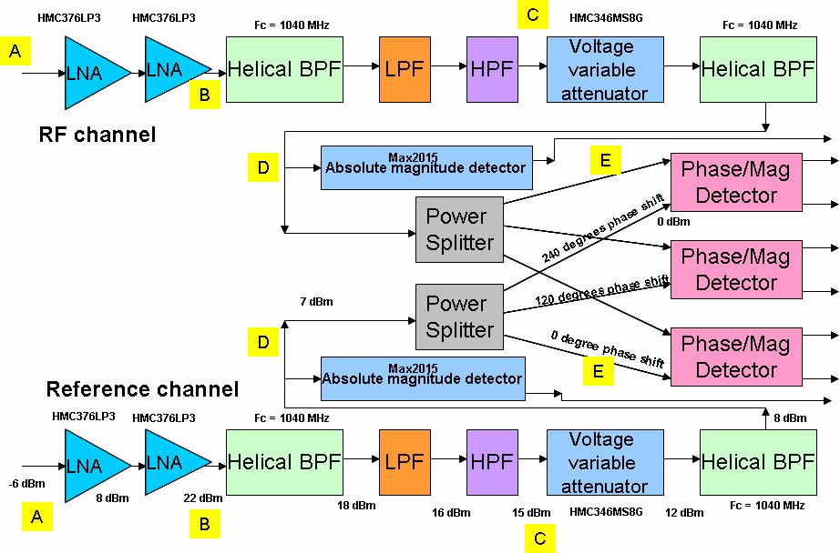
106 94
107 95
108 96 APPENDIX C. SIGNAL POWER LEVELS AND LEVEL DIAGRAMS IN THE TRANSCEIVER SYSTEM
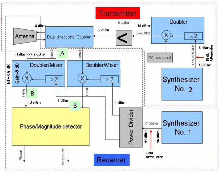
109 97
110 98
111 99 APPENDIX D. CIRCUIT DIAGRAM OF THE POWER SUPPLY BOARD
112 100
113 101 APPENDIX E. SYNTHESIZER S CHARACTERISTICS
114 102
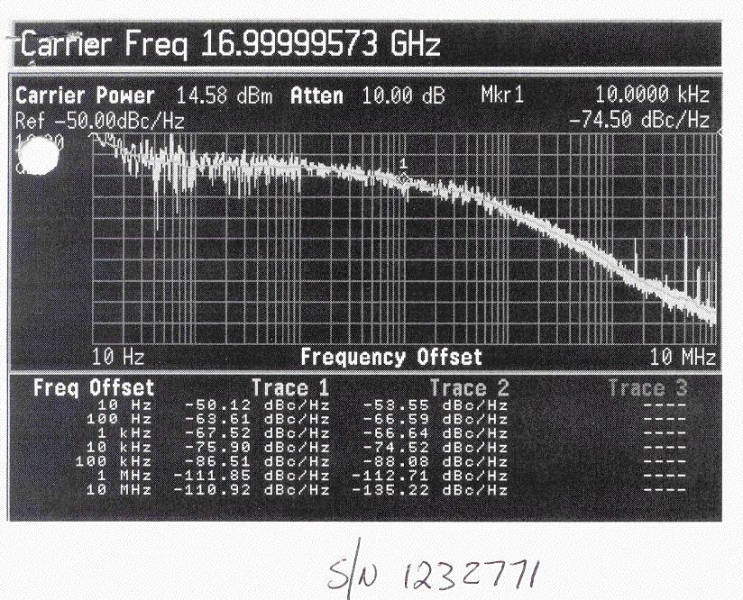
115 103
116 104
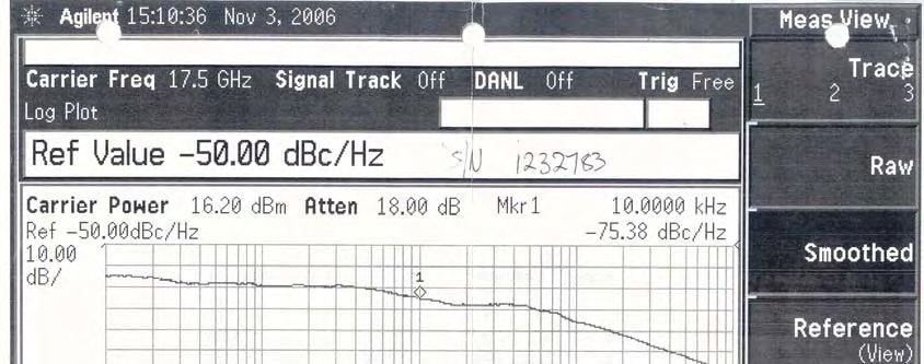
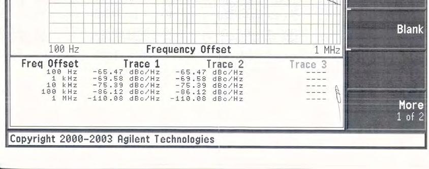
117 105
MICROWAVE MICROWAVE TRAINING BENCH COMPONENT SPECIFICATIONS:
 Microwave section consists of Basic Microwave Training Bench, Advance Microwave Training Bench and Microwave Communication Training System. Microwave Training System is used to study all the concepts of
Receiver Design. Prof. Tzong-Lin Wu EMC Laboratory Department of Electrical Engineering National Taiwan University 2011/2/21
 Receiver Design Prof. Tzong-Lin Wu EMC Laboratory Department of Electrical Engineering National Taiwan University 2011/2/21 MW & RF Design / Prof. T. -L. Wu 1 The receiver mush be very sensitive to -110dBm
Application Note 5525
 Using the Wafer Scale Packaged Detector in 2 to 6 GHz Applications Application Note 5525 Introduction The is a broadband directional coupler with integrated temperature compensated detector designed for
PART MAX2605EUT-T MAX2606EUT-T MAX2607EUT-T MAX2608EUT-T MAX2609EUT-T TOP VIEW IND GND. Maxim Integrated Products 1
 19-1673; Rev 0a; 4/02 EVALUATION KIT MANUAL AVAILABLE 45MHz to 650MHz, Integrated IF General Description The are compact, high-performance intermediate-frequency (IF) voltage-controlled oscillators (VCOs)
PA FAN PLATE ASSEMBLY 188D6127G1 SYMBOL PART NO. DESCRIPTION. 4 SBS /10 Spring nut. 5 19A702339P510 Screw, thread forming, flat head.
 MAINTENANCE MANUAL 851-870 MHz, 110 WATT POWER AMPLIFIER 19D902797G5 TABLE OF CONTENTS Page DESCRIPTION.............................................. Front Page SPECIFICATIONS.................................................
PARAMETER CONDITIONS TYPICAL PERFORMANCE Operating Supply Voltage 3.1V to 3.5V Supply Current V CC = 3.3V, LO applied 152mA
 DESCRIPTION LT5578 Demonstration circuit 1545A-x is a high linearity upconverting mixer featuring the LT5578. The LT 5578 is a high performance upconverting mixer IC optimized for output frequencies in
Linearity Improvement Techniques for Wireless Transmitters: Part 1
 From May 009 High Frequency Electronics Copyright 009 Summit Technical Media, LLC Linearity Improvement Techniques for Wireless Transmitters: art 1 By Andrei Grebennikov Bell Labs Ireland In modern telecommunication
Measurements 2: Network Analysis
 Measurements 2: Network Analysis Fritz Caspers CAS, Aarhus, June 2010 Contents Scalar network analysis Vector network analysis Early concepts Modern instrumentation Calibration methods Time domain (synthetic
A HILBERT TRANSFORM BASED RECEIVER POST PROCESSOR
 A HILBERT TRANSFORM BASED RECEIVER POST PROCESSOR 1991 Antenna Measurement Techniques Association Conference D. Slater Nearfield Systems Inc. 1330 E. 223 rd Street Bldg. 524 Carson, CA 90745 310-518-4277
Holography Transmitter Design Bill Shillue 2000-Oct-03
 Holography Transmitter Design Bill Shillue 2000-Oct-03 Planned Photonic Reference Distribution for Test Interferometer The transmitter for the holography receiver is made up mostly of parts that are already
772D coaxial dual-directional coupler 773D coaxial directional coupler. 775D coaxial dual-directional coupler 776D coaxial dual-directional coupler
 72 772D coaxial dual-directional coupler 773D coaxial directional coupler 775D coaxial dual-directional coupler 776D coaxial dual-directional coupler 777D coaxial dual-directional coupler 778D coaxial
Using Frequency Diversity to Improve Measurement Speed Roger Dygert MI Technologies, 1125 Satellite Blvd., Suite 100 Suwanee, GA 30024
 Using Frequency Diversity to Improve Measurement Speed Roger Dygert MI Technologies, 1125 Satellite Blvd., Suite 1 Suwanee, GA 324 ABSTRACT Conventional antenna measurement systems use a multiplexer or
Agilent Technologies PSA Series Spectrum Analyzers Test and Adjustment Software
 Test System Overview Agilent Technologies PSA Series Spectrum Analyzers Test and Adjustment Software Test System Overview The Agilent Technologies test system is designed to verify the performance of the
SC5407A/SC5408A 100 khz to 6 GHz RF Upconverter. Datasheet. Rev SignalCore, Inc.
 SC5407A/SC5408A 100 khz to 6 GHz RF Upconverter Datasheet Rev 1.2 2017 SignalCore, Inc. support@signalcore.com P R O D U C T S P E C I F I C A T I O N S Definition of Terms The following terms are used
Varactor-Tuned Oscillators. Technical Data. VTO-8000 Series
 Varactor-Tuned Oscillators Technical Data VTO-8000 Series Features 600 MHz to 10.5 GHz Coverage Fast Tuning +7 to +13 dbm Output Power ± 1.5 db Output Flatness Hermetic Thin-film Construction Description
CHAPTER 4. Practical Design
 CHAPTER 4 Practical Design The results in Chapter 3 indicate that the 2-D CCS TL can be used to synthesize a wider range of characteristic impedance, flatten propagation characteristics, and place passive
/14/$ IEEE 939
 Electro-Mechanical Structures for Channel Emulation Satyajeet Shinde #1, Sen Yang #2, Nicholas Erickson #3, David Pommerenke #4, Chong Ding *1, Douglas White *1, Stephen Scearce *1, Yaochao Yang *2 # Missouri
Receiver Architecture
 Receiver Architecture Receiver basics Channel selection why not at RF? BPF first or LNA first? Direct digitization of RF signal Receiver architectures Sub-sampling receiver noise problem Heterodyne receiver
Amplifier Characterization in the millimeter wave range. Tera Hertz : New opportunities for industry 3-5 February 2015
 Amplifier Characterization in the millimeter wave range Tera Hertz : New opportunities for industry 3-5 February 2015 Millimeter Wave Converter Family ZVA-Z500 ZVA-Z325 Y Band (WR02) ZVA-Z220 J Band (WR03)
The 144MHz Anglian 3 transverter
 The 144MHz Anglian 3 transverter A high performance 144/28MHz transverter G4DDK document issue 1 12/9/16 Introduction Anglian 3 is an update to the 144MHz Anglian 2 transverter. The Anglian 2 is no longer
Low Jitter, Low Emission Timing Solutions For High Speed Digital Systems. A Design Methodology
 Low Jitter, Low Emission Timing Solutions For High Speed Digital Systems A Design Methodology The Challenges of High Speed Digital Clock Design In high speed applications, the faster the signal moves through
Measurements with Scattering Parameter By Joseph L. Cahak Copyright 2013 Sunshine Design Engineering Services
 Measurements with Scattering Parameter By Joseph L. Cahak Copyright 2013 Sunshine Design Engineering Services Network Analyzer Measurements In many RF and Microwave measurements the S-Parameters are typically
Advances in Antenna Measurement Instrumentation and Systems
 Advances in Antenna Measurement Instrumentation and Systems Steven R. Nichols, Roger Dygert, David Wayne MI Technologies Suwanee, Georgia, USA Abstract Since the early days of antenna pattern recorders,
ABA GHz Broadband Silicon RFIC Amplifier. Application Note 1349
 ABA-52563 3.5 GHz Broadband Silicon RFIC Amplifier Application Note 1349 Introduction Avago Technologies ABA-52563 is a low current silicon gain block RFIC amplifier housed in a 6-lead SC 70 (SOT- 363)
A COMPACT, AGILE, LOW-PHASE-NOISE FREQUENCY SOURCE WITH AM, FM AND PULSE MODULATION CAPABILITIES
 A COMPACT, AGILE, LOW-PHASE-NOISE FREQUENCY SOURCE WITH AM, FM AND PULSE MODULATION CAPABILITIES Alexander Chenakin Phase Matrix, Inc. 109 Bonaventura Drive San Jose, CA 95134, USA achenakin@phasematrix.com
325 to 500 GHz Vector Network Analyzer System
 325 to 500 GHz Vector Network Analyzer System By Chuck Oleson, Tony Denning and Yuenie Lau OML, Inc. Abstract - This paper describes a novel and compact WR-02.2 millimeter wave frequency extension transmission/reflection
Comparison of Focused and Near-Field Imaging of Spray on Foam Insulation (SOFI) at Millimeter Wave Frequencies
 at Millimeter Wave Frequencies") Missouri University of Science and Technology Scholars' Mine Electrical and Computer Engineering Faculty Research & Creative Works Electrical and Computer Engineering 6-1-2007 Comparison of Focused and
Missouri University of Science and Technology Scholars' Mine Electrical and Computer Engineering Faculty Research & Creative Works Electrical and Computer Engineering 6-1-2007 Comparison of Focused and
Chapter 6. Case Study: 2.4-GHz Direct Conversion Receiver. 6.1 Receiver Front-End Design
 Chapter 6 Case Study: 2.4-GHz Direct Conversion Receiver The chapter presents a 0.25-µm CMOS receiver front-end designed for 2.4-GHz direct conversion RF transceiver and demonstrates the necessity and
10 GHz Microwave Link
 10 GHz Microwave Link Project Project Objectives System System Functionality Testing Testing Procedures Cautions and Warnings Problems Encountered Recommendations Conclusion PROJECT OBJECTIVES Implement
87415A microwave system amplifier A microwave. system amplifier A microwave system amplifier A microwave.
 20 Amplifiers 83020A microwave 875A microwave 8308A microwave 8307A microwave 83006A microwave 8705C preamplifier 8705B preamplifier 83050/5A microwave The Agilent 83006/07/08/020/050/05A test s offer
Analysis of RF transceivers used in automotive
 Scientific Bulletin of Politehnica University Timisoara TRANSACTIONS on ELECTRONICS and COMMUNICATIONS Volume 60(74), Issue, 0 Analysis of RF transceivers used in automotive Camelia Loredana Ţeicu Abstract
Ultra High Frequency Measurements
 Ultra High Frequency Measurements Desmond Fraser desmond@rheintech.com 703.689.0368 360 Herndon Parkway Suite 1400 Herndon, VA 20170 IEEE EMC DC / N. VA Chapter 31 January 2012 Overview We ll review Millimeter
Maintenance Manual LBI-38531G MHz, 110 WATT POWER AMPLIFIER 19D902797G1 DESCRIPTION TABLE OF CONTENTS
 Maintenance Manual LBI-38531G 136-174 MHz, 110 WATT POWER AMPLIFIER 19D902797G1 TABLE OF CONTENTS Page DESCRIPTION.............................................. Front Cover SPECIFICATIONS.................................................
SC5307A/SC5308A 100 khz to 6 GHz RF Downconverter. Datasheet SignalCore, Inc.
 SC5307A/SC5308A 100 khz to 6 GHz RF Downconverter Datasheet 2017 SignalCore, Inc. support@signalcore.com P RODUCT S PECIFICATIONS Definition of Terms The following terms are used throughout this datasheet
TECHNICAL INFORMATION
 TECHNICAL INFORMATION TECHNOLOGY Y-Junction circulator PORT 1 PORT 2 PORT 3 FIG. 1 The Y-junction circulator uses spinel ferrites or garnet ferrites in the presence of a magnetic bias field, to provide
IN propagation path between the satellite and
 Journal of Advances in Computer Engineering and Technology, 1(2) 215 Typical Ka band Satellite Beacon Receiver Design for Propagation Experimentation Reza Bahri 1, Hossein Yarmohammadi 2, Mohammadreza
1 of 7 12/20/ :04 PM
 1 of 7 12/20/2007 11:04 PM Trusted Resource for the Working RF Engineer [ C o m p o n e n t s ] Build An E-pHEMT Low-Noise Amplifier Although often associated with power amplifiers, E-pHEMT devices are
DEVELOPMENT AND PRODUCTION OF HYBRID CIRCUITS FOR MICROWAVE RADIO LINKS
 Electrocomponent Science and Technology 1977, Vol. 4, pp. 79-83 (C)Gordon and Breach Science Publishers Ltd., 1977 Printed in Great Britain DEVELOPMENT AND PRODUCTION OF HYBRID CIRCUITS FOR MICROWAVE RADIO
UNIT-3. Electronic Measurements & Instrumentation
 UNIT-3 1. Draw the Block Schematic of AF Wave analyzer and explain its principle and Working? ANS: The wave analyzer consists of a very narrow pass-band filter section which can Be tuned to a particular
Application Note 5057
 A 1 MHz to MHz Low Noise Feedback Amplifier using ATF-4143 Application Note 7 Introduction In the last few years the leading technology in the area of low noise amplifier design has been gallium arsenide
Optical Delay Line Application Note
 1 Optical Delay Line Application Note 1.1 General Optical delay lines system (ODL), incorporates a high performance lasers such as DFBs, optical modulators for high operation frequencies, photodiodes,
Session 3. CMOS RF IC Design Principles
 Session 3 CMOS RF IC Design Principles Session Delivered by: D. Varun 1 Session Topics Standards RF wireless communications Multi standard RF transceivers RF front end architectures Frequency down conversion
The Schottky Diode Mixer. Application Note 995
 The Schottky Diode Mixer Application Note 995 Introduction A major application of the Schottky diode is the production of the difference frequency when two frequencies are combined or mixed in the diode.
Student Research & Creative Works
 Scholars' Mine Masters Theses Student Research & Creative Works Spring 2017 Characterization of the rectification behaviour of in-amps and estimating the near field coupling from SMPS circuits to a nearby
RADIO RECEIVERS ECE 3103 WIRELESS COMMUNICATION SYSTEMS
 RADIO RECEIVERS ECE 3103 WIRELESS COMMUNICATION SYSTEMS FUNCTIONS OF A RADIO RECEIVER The main functions of a radio receiver are: 1. To intercept the RF signal by using the receiver antenna 2. Select the
Keysight Technologies Pulsed Antenna Measurements Using PNA Network Analyzers
 Keysight Technologies Pulsed Antenna Measurements Using PNA Network Analyzers White Paper Abstract This paper presents advances in the instrumentation techniques that can be used for the measurement and
Keywords: ISM, RF, transmitter, short-range, RFIC, switching power amplifier, ETSI
 Maxim > Design Support > Technical Documents > Application Notes > Wireless and RF > APP 4929 Keywords: ISM, RF, transmitter, short-range, RFIC, switching power amplifier, ETSI APPLICATION NOTE 4929 Adapting
Vector Network Analyzer
 Vector Network Analyzer VNA Basics VNA Roadshow Budapest 17/05/2016 Content Why Users Need VNAs VNA Terminology System Architecture Key Components Basic Measurements Calibration Methods Accuracy and Uncertainty
Varactor-Tuned Oscillators. Technical Data. VTO-8000 Series. Pin Configuration TO-8V
 H Varactor-Tuned Oscillators Technical Data VTO-8 Series Features 6 MHz to.5 Coverage Fast Tuning +7 to + dbm Output Power ±1.5 db Output Flatness Hermetic Thin-film Construction Description HP VTO-8 Series
Configuration of PNA-X, NVNA and X parameters
 Configuration of PNA-X, NVNA and X parameters VNA 1. S-Parameter Measurements 2. Harmonic Measurements NVNA 3. X-Parameter Measurements Introducing the PNA-X 50 GHz 43.5 GHz 26.5 GHz 13.5 GHz PNA-X Agilent
AV3672 Series Vector Network Analyzer
 AV3672 Series Vector Network Analyzer AV3672A/B/C/D/E (10MHz 13.5 GHz/26.5 GHz/43.5 GHz/50 GHz/67 GHz) Product Overview: AV3672 series vector network analyzer include AV3672A (10MHz 13.5GHz), AV3672B (10MHz
Microwave and Millimeter Wave Testing for the Inspection of the Space Shuttle Spray on Foam Insulation (SOFI) and the Acreage Heat Tiles
 and the Acreage Heat Tiles") Missouri University of Science and Technology Scholars' Mine Electrical and Computer Engineering Faculty Research & Creative Works Electrical and Computer Engineering 7--2005 Microwave and Millimeter Wave
Missouri University of Science and Technology Scholars' Mine Electrical and Computer Engineering Faculty Research & Creative Works Electrical and Computer Engineering 7--2005 Microwave and Millimeter Wave
Overview of the MSA 12/30/10
 Overview of the MSA 12/30/10 Introduction The purpose of this document is to provide an overview of the capabilities and construction of the MSA to help potential builders get oriented. Much more detailed
HP Archive. This vintage Hewlett Packard document was preserved and distributed by www. hparchive.com Please visit us on the web!
 HP Archive This vintage Hewlett Packard document was preserved and distributed by www. hparchive.com Please visit us on the web! On-line curator: Glenn Robb This document is for FREE distribution only!
Development of Signal Analyzer MS2840A with Built-in Low Phase-Noise Synthesizer
 Development of Signal Analyzer MS2840A with Built-in Low Phase-Noise Synthesizer Toru Otani, Koichiro Tomisaki, Naoto Miyauchi, Kota Kuramitsu, Yuki Kondo, Junichi Kimura, Hitoshi Oyama [Summary] Evaluation
Low Distortion Mixer AD831
 a FEATURES Doubly-Balanced Mixer Low Distortion +2 dbm Third Order Intercept (IP3) + dbm 1 db Compression Point Low LO Drive Required: dbm Bandwidth MHz RF and LO Input Bandwidths 2 MHz Differential Current
Design and Matching of a 60-GHz Printed Antenna
 Application Example Design and Matching of a 60-GHz Printed Antenna Using NI AWR Software and AWR Connected for Optenni Figure 1: Patch antenna performance. Impedance matching of high-frequency components
CUSTOM INTEGRATED ASSEMBLIES
 17 CUSTOM INTEGRATED ASSEMBLIES CUSTOM INTEGRATED ASSEMBLIES Cougar offers full first-level integration capabilities, providing not just performance components but also full subsystem solutions to help
Millimeter Wave Product Catalogue VivaTech Consulting S.A.R.L.
 VivaTech Consulting S.A.R.L. sales@vivatech.biz Telephone: +33 04 89 01 14 61 Fax: +33 04 93 87 08 66 Table of Contents Millimeter Wave Low Noise Amplifiers VTLNA Series...3 Millimeter Wave Power Amplifiers
433MHz front-end with the SA601 or SA620
 433MHz front-end with the SA60 or SA620 AN9502 Author: Rob Bouwer ABSTRACT Although designed for GHz, the SA60 and SA620 can also be used in the 433MHz ISM band. The SA60 performs amplification of the
CHAPTER - 6 PIN DIODE CONTROL CIRCUITS FOR WIRELESS COMMUNICATIONS SYSTEMS
 CHAPTER - 6 PIN DIODE CONTROL CIRCUITS FOR WIRELESS COMMUNICATIONS SYSTEMS 2 NOTES 3 INTRODUCTION PIN DIODE CONTROL CIRCUITS FOR WIRELESS COMMUNICATIONS SYSTEMS Chapter 6 discusses PIN Control Circuits
Antenna and RCS Measurement Configurations Using Agilent s New PNA Network Analyzers
 Antenna and RCS Measurement Configurations Using Agilent s New PNA Network Analyzers John Swanstrom, Application Engineer, Agilent Technologies, Santa Rosa, CA Jim Puri, Applications Engineer, Agilent
Driver Amplifier for 7 Tesla MRI Smart Power Amplifier
 Driver Amplifier for 7 Tesla MRI Smart Power Amplifier presented by Kevin Kolpatzeck supervised by Prof. Dr.-Ing. Klaus Solbach Institute of Microwave and RF Technology University of Duisburg Essen Contents
Application Note 1360
 ADA-4743 +17 dbm P1dB Avago Darlington Amplifier Application Note 1360 Description Avago Technologies Darlington Amplifier, ADA-4743 is a low current silicon gain block RFIC amplifier housed in a 4-lead
ALMA MEMO #360 Design of Sideband Separation SIS Mixer for 3 mm Band
 ALMA MEMO #360 Design of Sideband Separation SIS Mixer for 3 mm Band V. Vassilev and V. Belitsky Onsala Space Observatory, Chalmers University of Technology ABSTRACT As a part of Onsala development of
Agilent Antenna and RCS Measurement Configurations Using PNA Microwave Network Analyzers. White Paper
 Agilent Antenna and RCS Measurement Configurations Using PNA Microwave Network Analyzers White Paper Abstract As technology changes, new and different techniques for measuring and characterizing antenna
Design of a current probe for measuring ball-gridarray packaged devices
 Scholars' Mine Masters Theses Student Research & Creative Works Fall 2011 Design of a current probe for measuring ball-gridarray packaged devices Tianqi Li Follow this and additional works at: http://scholarsmine.mst.edu/masters_theses
Direct-Conversion I-Q Modulator Simulation by Andy Howard, Applications Engineer Agilent EEsof EDA
 Direct-Conversion I-Q Modulator Simulation by Andy Howard, Applications Engineer Agilent EEsof EDA Introduction This article covers an Agilent EEsof ADS example that shows the simulation of a directconversion,
L AND S BAND TUNABLE FILTERS PROVIDE DRAMATIC IMPROVEMENTS IN TELEMETRY SYSTEMS
 L AND S BAND TUNABLE FILTERS PROVIDE DRAMATIC IMPROVEMENTS IN TELEMETRY SYSTEMS Item Type text; Proceedings Authors Wurth, Timothy J.; Rodzinak, Jason Publisher International Foundation for Telemetering
Phase Noise and Tuning Speed Optimization of a MHz Hybrid DDS-PLL Synthesizer with milli Hertz Resolution
 Phase Noise and Tuning Speed Optimization of a 5-500 MHz Hybrid DDS-PLL Synthesizer with milli Hertz Resolution BRECHT CLAERHOUT, JAN VANDEWEGE Department of Information Technology (INTEC) University of
ECEN 5014, Spring 2009 Special Topics: Active Microwave Circuits Zoya Popovic, University of Colorado, Boulder
 ECEN 5014, Spring 2009 Special Topics: Active Microwave Circuits Zoya opovic, University of Colorado, Boulder LECTURE 3 MICROWAVE AMLIFIERS: INTRODUCTION L3.1. TRANSISTORS AS BILATERAL MULTIORTS Transistor
GHz-band, high-accuracy SAW resonators and SAW oscillators
 The evolution of wireless communications and semiconductor technologies is spurring the development and commercialization of a variety of applications that use gigahertz-range frequencies. These new applications
RFID Systems: Radio Architecture
 RFID Systems: Radio Architecture 1 A discussion of radio architecture and RFID. What are the critical pieces? Familiarity with how radio and especially RFID radios are designed will allow you to make correct
PRODUCT APPLICATION NOTES
 Extending the HMC189MS8 Passive Frequency Doubler Operating Range with External Matching General Description The HMC189MS8 is a miniature passive frequency doubler in a plastic 8-lead MSOP package. The
SynthNV - Signal Generator / Power Detector Combo
 SynthNV - Signal Generator / Power Detector Combo The Windfreak SynthNV is a 34.4MHz to 4.4GHz software tunable RF signal generator controlled and powered by a PC running Windows XP, Windows 7, or Android
Windfreak Technologies SynthHD v1.4 Preliminary Data Sheet v0.2b
 Windfreak Technologies SynthHD v1.4 Preliminary Data Sheet v0.2b $1299.00US 54 MHz 13.6 GHz Dual Channel RF Signal Generator Features Open source Labveiw GUI software control via USB Run hardware functions
MAKING TRANSIENT ANTENNA MEASUREMENTS
 MAKING TRANSIENT ANTENNA MEASUREMENTS Roger Dygert, Steven R. Nichols MI Technologies, 1125 Satellite Boulevard, Suite 100 Suwanee, GA 30024-4629 ABSTRACT In addition to steady state performance, antennas
Television and video engineering
 Television and video engineering Unit-4 Television Receiver systems Objectives: To learn the requirements of TV receiver Study of monochrome and Colour TV receivers. To learn functions of Tuning circuits
UNIT 2. Q.1) Describe the functioning of standard signal generator. Ans. Electronic Measurements & Instrumentation
 Describe the functioning of standard signal generator. Ans. Electronic Measurements & Instrumentation") UNIT 2 Q.1) Describe the functioning of standard signal generator Ans. STANDARD SIGNAL GENERATOR A standard signal generator produces known and controllable voltages. It is used as power source for the
UNIT 2 Q.1) Describe the functioning of standard signal generator Ans. STANDARD SIGNAL GENERATOR A standard signal generator produces known and controllable voltages. It is used as power source for the
Digital Step Attenuators offer Precision and Linearity
 Digital Step Attenuators offer Precision and Linearity (AN-70-004) DAT Attenuator (Surface Mount) Connectorized DAT attenuator (ZX76 Series) Connectorized DAT attenuator ZX76-31R5-PN attenuator with parallel
Design and Layout of a X-Band MMIC Power Amplifier in a Phemt Technology
 Design and Layout of a X-Band MMIC Power Amplifier in a Phemt Technology Renbin Dai, and Rana Arslan Ali Khan Abstract The design of Class A and Class AB 2-stage X band Power Amplifier is described in
Fabricate a 2.4-GHz fractional-n synthesizer
 University of Malaya From the SelectedWorks of Professor Mahmoud Moghavvemi Summer June, 2013 Fabricate a 2.4-GHz fractional-n synthesizer H Ameri Mahmoud Moghavvemi, University of Malaya a Attaran Available
RF/Microwave Circuits I. Introduction Fall 2003
 Introduction Fall 03 Outline Trends for Microwave Designers The Role of Passive Circuits in RF/Microwave Design Examples of Some Passive Circuits Software Laboratory Assignments Grading Trends for Microwave
EMI measurement and modeling techniques for complex electronic circuits and modules
 Scholars' Mine Doctoral Dissertations Student Theses and Dissertations Summer 2017 EMI measurement and modeling techniques for complex electronic circuits and modules Satyajeet Shinde Follow this and additional
Technical Article A DIRECT QUADRATURE MODULATOR IC FOR 0.9 TO 2.5 GHZ WIRELESS SYSTEMS
 Introduction As wireless system designs have moved from carrier frequencies at approximately 9 MHz to wider bandwidth applications like Personal Communication System (PCS) phones at 1.8 GHz and wireless
Termination Insensitive Mixers By Howard Hausman President/CEO, MITEQ, Inc. 100 Davids Drive Hauppauge, NY
 Termination Insensitive Mixers By Howard Hausman President/CEO, MITEQ, Inc. 100 Davids Drive Hauppauge, NY 11788 hhausman@miteq.com Abstract Microwave mixers are non-linear devices that are used to translate
Manufacturers of RF and Microwave Components and Assemblies Specialist in RF Filters, Power amplifiers and RF Switches
 Manufacturers of RF and Microwave Components and Assemblies Specialist in RF Filters, Power amplifiers and RF Switches sales@cormic.com www.cormic.com P 724.940.7556 F 724.940.7707 RF & MICROWAVE FILTERS
Low Cost Mixer for the 10.7 to 12.8 GHz Direct Broadcast Satellite Market
 Low Cost Mixer for the.7 to 12.8 GHz Direct Broadcast Satellite Market Application Note 1136 Introduction The wide bandwidth requirement in DBS satellite applications places a big performance demand on
EVALUATION KIT AVAILABLE 10MHz to 1050MHz Integrated RF Oscillator with Buffered Outputs. Typical Operating Circuit. 10nH 1000pF MAX2620 BIAS SUPPLY
 19-1248; Rev 1; 5/98 EVALUATION KIT AVAILABLE 10MHz to 1050MHz Integrated General Description The combines a low-noise oscillator with two output buffers in a low-cost, plastic surface-mount, ultra-small
A NEW GENERATION PROGRAMMABLE PHASE/AMPLITUDE MEASUREMENT RECEIVER
 GENERAL A NEW GENERATION PROGRAMMABLE PHASE/AMPLITUDE MEASUREMENT RECEIVER by Charles H. Currie Scientific-Atlanta, Inc. 3845 Pleasantdale Road Atlanta, Georgia 30340 A new generation programmable, phase-amplitude
S-Band 2.4GHz FMCW Radar
 S-Band 2.4GHz FMCW Radar Iulian Rosu, YO3DAC / VA3IUL, Filip Rosu, YO3JMK, http://qsl.net/va3iul A Radar detects the presence of objects and locates their position in space by transmitting electromagnetic
Agilent 8360B/8360L Series Synthesized Swept Signal/CW Generators 10 MHz to 110 GHz
 Agilent 8360B/8360L Series Synthesized Swept Signal/CW Generators 10 MHz to 110 GHz ity. l i t a ers V. n isio c e r P. y t i l i ib Flex 2 Agilent 8360 Synthesized Swept Signal and CW Generator Family
MICROWAVE AND RADAR LAB (EE-322-F) LAB MANUAL VI SEMESTER
 LAB MANUAL VI SEMESTER") 1 MICROWAVE AND RADAR LAB (EE-322-F) MICROWAVE AND RADAR LAB (EE-322-F) LAB MANUAL VI SEMESTER RAO PAHALD SINGH GROUP OF INSTITUTIONS BALANA(MOHINDERGARH)123029 Department Of Electronics and Communication
1 MICROWAVE AND RADAR LAB (EE-322-F) MICROWAVE AND RADAR LAB (EE-322-F) LAB MANUAL VI SEMESTER RAO PAHALD SINGH GROUP OF INSTITUTIONS BALANA(MOHINDERGARH)123029 Department Of Electronics and Communication
A calibration free vector network analyzer
 Scholars' Mine Masters Theses Student Research & Creative Works Summer 2013 A calibration free vector network analyzer Arpit Kothari Follow this and additional works at: http://scholarsmine.mst.edu/masters_theses
SDARS: Front End Antenna Design. Keven Lockwood Advisor: Dr. Prasad Shastry
 SDARS: Front End Antenna Design Keven Lockwood Advisor: Dr. Prasad Shastry 1 Outline Project Overview Antenna Characteristics Feeding Techniques Performance Specifications Design Process Expected results
RF Components Product Catalogue
 RF Components Product Catalogue Government and Defence Broadcast Marine, Oil and Gas SNG and VSAT RF Engineering by Design Contents Splitters / Combiners Active Splitters and Combiners Page 3 Passive Splitters
Platform Migration 8510 to PNA. Graham Payne Application Engineer Agilent Technologies
 Platform Migration 8510 to PNA Graham Payne Application Engineer Agilent Technologies We set the standard... 8410 8510 When we introduced the 8510, we changed the way S-parameter measurements were made!
GaAs MMIC devices are susceptible to Electrostatic Discharge. Use proper ESD precautions when handling these items.
 The is a broadband, power efficient GaAs PHEMT distributed amplifier in a 4mm QFN surface mount package. The is designed to provide optimal LO drive for T3 mixers. Typically, ADM-26-2931SM provides. db
Demo board DC365A Quick Start Guide.
 August 02, 2001. Demo board DC365A Quick Start Guide. I. Introduction The DC365A demo board is intended to demonstrate the capabilities of the LT5503 RF transmitter IC. This IC incorporates a 1.2 GHz to
Application Note 5011
 MGA-62563 High Performance GaAs MMIC Amplifier Application Note 511 Application Information The MGA-62563 is a high performance GaAs MMIC amplifier fabricated with Avago Technologies E-pHEMT process and