4H-SiC Power Bipolar Junction Transistor with a Very Low Specific On-resistance of 2.9 mω.cm 2
|
|
|
- Cora Baldwin
- 6 years ago
- Views:
Transcription
1 4H-SiC Power Bipolar Junction Transistor with a Very Low Specific On-resistance of 2.9 mω.cm 2 Jianhui Zhang, member, IEEE, Petre Alexandrov, member, IEEE, Terry Burke, member, IEEE, and Jian H. Zhao, Senior Member, IEEE, Abstract This paper reports a newly achieved best result on the specific on-resistance (Rsp,on) of power 4H-SiC bipolar junction transistors (BJT). A 4H-SiC BJT based on a 12 um drift-layer shows a record low specific-on resistance of only 2.9 mω.cm 2, with an open base collector-to-emitter blocking voltage (Vceo) of 757 V, and a current gain of The active area of this 4H-SiC BJT is 0.61 mm 2, and it has a fully inter-digitated design. This high performance 4H-SiC BJT conducts up to 5.24 A at a forward voltage drop of V CE = 2.5 V, corresponding to a low Rsp_on of 2.9 mω.cm 2 up to Jc=859 A/cm 2. This is the lowest specific on-resistance ever reported for high power 4H-SiC BJTs. Index Terms Silicon carbide, bipolar junction transistors (BJTs), power transistors Jianhui Zhang, and Petre Alexandrov are with United Silicon Carbide, Inc, New Brunswick Technology Center, New Brunswick, NJ 08901, USA and both are part time students with Rutgers University. Terry Burke is with U.S. Army TACOM, Warren, MI 48397, Jian H. Zhao is with SiCLAB, ECE Department, Rutgers University, Piscataway, NJ 08854, USA. 1
2 Report Documentation Page Form Approved OMB No Public reporting burden for the collection of information is estimated to average 1 hour per response, including the time for reviewing instructions, searching existing data sources, gathering and maintaining the data needed, and completing and reviewing the collection of information. Send comments regarding this burden estimate or any other aspect of this collection of information, including suggestions for reducing this burden, to Washington Headquarters Services, Directorate for Information Operations and Reports, 1215 Jefferson Davis Highway, Suite 1204, Arlington VA Respondents should be aware that notwithstanding any other provision of law, no person shall be subject to a penalty for failing to comply with a collection of information if it does not display a currently valid OMB control number. 1. REPORT DATE 12 APR REPORT TYPE N/A 3. DATES COVERED - 4. TITLE AND SUBTITLE 4H-SiC Power Bipolar Junction Transistor with a Very Low Specific On-resistance of 2.9 mù.cm2 6. AUTHOR(S) Jianhui Zhang; Petre Alexandrov; Terry Burke; Jian H. Zhao 5a. CONTRACT NUMBER 5b. GRANT NUMBER 5c. PROGRAM ELEMENT NUMBER 5d. PROJECT NUMBER 5e. TASK NUMBER 5f. WORK UNIT NUMBER 7. PERFORMING ORGANIZATION NAME(S) AND ADDRESS(ES) US Army RDECOM-TARDEC 6501 E 11 Mile Rd Warren, MI , USA United Silicon Carbide, Inc, New Brunswick Technology Center, New Brunswick, NJ 08901, USA SiCLAB, ECE Department, Rutgers University, Piscataway, NJ 08854, USA. 8. PERFORMING ORGANIZATION REPORT NUMBER SPONSORING/MONITORING AGENCY NAME(S) AND ADDRESS(ES) 10. SPONSOR/MONITOR S ACRONYM(S) TACOM/TARDEC 12. DISTRIBUTION/AVAILABILITY STATEMENT Approved for public release, distribution unlimited 13. SUPPLEMENTARY NOTES The original document contains color images. 14. ABSTRACT 15. SUBJECT TERMS 11. SPONSOR/MONITOR S REPORT NUMBER(S) SECURITY CLASSIFICATION OF: 17. LIMITATION OF ABSTRACT SAR a. REPORT unclassified b. ABSTRACT unclassified c. THIS PAGE unclassified 18. NUMBER OF PAGES 13 19a. NAME OF RESPONSIBLE PERSON Standard Form 298 (Rev. 8-98) Prescribed by ANSI Std Z39-18
3 I. INTRODUCTION Silicon Carbide electronic devices have got more and more attentions recently due to its wide band-gap material properties and fast-maturing technologies. 4H-SiC (Eg=3.26 ev) bipolar junction transistor (BJT) is an important switching device for high power and high temperature applications, which is an intrinsically normally-off device, does not have the gate oxide problems and conducts higher current with low forward voltage drop. For a power 4H-SiC BJT device, high blocking voltage [1], low on-state resistance and high current gain [2,3] are desirable for better efficiency. The most recently reported high power 4H-SiC BJTs with a low specific on-resistance (Rsp,on) include (i) a Vceo = 1400 V, 17 A BJT showing a current gain of 14 and an R SP_ON of 5.3 mω cm 2 [4]; (ii) a Vceo = 1450 V BJT with a current gain of 14 and an R SP_ON of 5.4 mω cm 2 [5]; (iii) a 1000 V BJT with a current gain of 40 and an R SP_ON of 6.0 mω cm 2 [6]; (iv) a 1677 V, 5.7 mω cm 2 4H-SiC BJT with a current gain of 7.1 [7]; (v) a 1600 V-20 A 4H-SiC BJT with Rsp,on=4.5 mω cm 2 and a current gain of 40 [8]; (vi) a 3200 V, 10 A 4H-SiC BJT with a current gain of 44 and a specific on-resistance of 8.1 mω cm 2 [9]; (vii) a 1836V, 4.7 mω cm 2 4H-SiC BJT with a current gain of 8.8 [10]. This paper reports a newly developed 4H-SiC BJT with a record low specific on-resistance (R SP_ON ) of only 2.9 mω cm 2 up to Jc = 859 A/cm 2, a high blocking voltage V B (Vceo ) of 757 V and a good DC current gain(ic/ib) of II. DEVICE DESIGN AND FABRICATION Fig.1 shows a simplified cross-sectional view of the 4H-SiC BJT structure. The 4H-SiC wafer was purchased from Cree Inc. Three epi-layers are grown on the 8 o off-axis n-type 2
4 4H-SiC substrate. The top n + epi-layer of 0.8 μm is heavily doped to about cm -3 to serve as the emitter. The base p-type epi-layer is 1.0 μm thick and is doped to cm -3. The collector drift layer of 12 μm is lightly-doped to cm -3. The fabrication process starts from the dry-etching of the emitter fingers by inductively coupled plasma (ICP) etching in a gas mixture of freon and oxygen at an etching rate of nm/min. The emitter finger width is 10 um and the etching depth is 1.0 μm. The p-type epi-layer was exposed in the base trench and the JTE region. To achieve better base ohmic contact, a 3 um-wide region in the center of the 13 um-wide base trench was implanted at room temperature with carbon and aluminum co-implantation [11], which consists of C ions of 4x10 14 cm -2 at 28keV, 5.2x10 14 cm -2 at 60 kev, and 1.1x10 14 cm -2 at 75 kev plus Al ions of 3.6x10 14 cm -2 at 50 kev and 7.5x10 14 cm -2 at 100 kev. The spacing between the implanted base region and the emitter mesa edge (BE-spacing) is 5 μm. The ion-implantation activation annealing was done at 1550 o C for 30 min in Ar ambient. Device edge termination applied a single step JTE of 150 μm-wide based on an ion-implanted p-layer and the base epi-layer. The isolation between each device is served by a mesa etching of ~1.5 μm into the drift layer. Surface passivation was first done by a regular wet thermal oxidation for 2 hours at 1100 o C followed by a one-hour Ar annealing at 1100 o C, then the sample was re-annealed in wet-oxygen for 3 hours at 950 o C. After the thermal oxidation, 500 nm SiO 2 and 250 nm Si 3 N 4 were deposited by PECVD to seal the thermal passivation layer. Device contact windows were opened by ICP etching and wet-etching, Ni/AlTi/Ni was sputtered on the base contact region, Ni was sputtered on the emitter contact region and the collector. The Ohmic contact annealing was carried out at 1000 o C for 5 minutes in Argon forming gas (5% H 2 in Ar) by using a rapid thermal 3
5 processing (RTP) system. After Ohmic contact formation, about 3 um Al/AlTi was sputtered and wet-etched to form a thick overlay metal on the base and emitter fingers to improve the voltage and current distribution. Then, 1.4 μm multi-layer of SiO 2 and Si 3 N 4 were deposited by PECVD to cover all the sample surface. The contact windows for the base bonding pad, the emitter bonding pad and the emitter fingers were opened by ICP, and over 0.5 um Ti / Au were deposited. Fig.2 shows a photo of the fabricated 4H-SiC BJT device. The 4H-SiC BJT device has a footprint of 1.2 mm 1.4 mm including the bonding pads and the JTE region. This BJT device contains 37 emitter fingers and 38 base fingers in a fully inter-digitated geometry. The finger length is 728 μm, and the width of the emitter mesa and base trench are 10 μm and 13 μm, respectively. Excluding the bonding pads and the edge termination region, the device active area is 0.61 mm 2. III. EXPERIMENTAL RESULTS AND DISCUSSIONS Measured from the on-chip TLM (transmission line model) structure, the emitter n-type specific contact resistance and n + emitter layer sheet resistance are Ω cm 2 and 147 Ω, respectively, while the p-type specific contact resistance and p-base sheet resistance are Ω cm 2 and 33 kω, respectively. The device DC I-V characteristics were measured mainly by Tektronix 371A curve tracer. Fig. 3 shows the I-V characteristics of a single 4H-SiC BJT cell at room temperature. This BJT device conducts 5.24 A collector current (Jc = 859 A/cm 2 ) at a forward voltage drop of 2.5 V, corresponding to a specific on- resistance of only 2.9 mω cm 2. This is so far the lowest specific on-resistance ever reported for 4H-SiC bipolar 4
6 transistors. The maximum collector current was measured up to 8.2 A (Jc = 1344 A/cm 2 ) and is actually limited by the capability of Tektronix 371A curve tracer. The DC current gain is 18.8 at Ic=3.75 A (Jc=615 A/cm2) and Vce=4.6 V. The open base blocking voltage (Vceo) was measured up to 757 V with 231 μa leakage current in Fluorinert. The key to achieving this record low specific on-resistance is biasing the base-emitter junction uniformly so that each part of the active area works homogeneously. Therefore, the base overlay metal plays a critical role, which carries the base current from the bonding pad to the end of each base fingers. We reported two similar 4H-SiC BJTs before [7,10] with nearly same active area. The 5.7 mω cm 2 BJT device [7] has 0.4 um Ti/Au as the base overlay metal, and its base contact region is as wide as 11 um. We pointed out in that paper that the BE junction needs to be more uniformly biased. Therefore, in the following batch of our 4H-SiC BJT study, we put down about 2.1 um AlTi/Mo as the base overlay metal, and reduced the pitch from 33 um to 22 um. That BJT device shows an absolute specific on-resistance of 4.7 mω cm 2 and a differential specific on-resistance of only 3.9 mω cm 2 [10]. But the current gain of the both previous BJTs is only about 7.1 and 8.8, which requires large base current to be distributed across the whole device active area, thus even thicker base metal might be needed. In the 4H- SiC BJT reported in this paper, we successfully got the current gain (Ic/Ib) as high as 18.8, which significantly reduces the required base driving current, and we still put down 3.0 um Al/AlTi as the base overlay metal. Hence we have successfully achieved this record low specific on-resistance of only 2.9 mω cm 2. Fig.4 shows the forward I-V characteristics of the base-emitter (BE) junctions of this 2.9 mω cm 2 BJT device and the earlier 4.7 mω cm 2 BJT device. Clearly, we could see a big improvement on the BE 5
7 junction forward I-V characteristics, and we believe it leads to a more uniformly-biased BE junctions across the whole device area. It has been proved that the current gain of 4H-SiC BJTs is more determined by the epilayer growth process rather than the device fabrication process [3,6,7,8,9,12]. On a similar 4H-SiC BJT wafer we fabricated before, the current gain was about 24.8 [12]. The blocking performance (Vceo=757V) on this 4H-SiC BJT only reaches about half of its theoretical value, which is due to the excessive SiC consumption in the JTE region during the thermal oxidation process. IV. SUMMARY A 4H-SiC power BJT with a record low specific on-resistance of 2.9 mω cm 2 has been demonstrated based on a drift layer of 12 μm doped to 8.5x10 15 cm -3. The blocking voltage V B (Vceo) is 757 V, and the current gain is The uniform biasing of baseemitter junction across the whole device active area is the key to achieving this best result on the specific on-resistance. Acknowledgment: Authors at RU acknowledge financial support provided by United Silicon Carbide, Inc. Work at USCI was supported in part by a TACOM SBIR program (DAAE07-02-C-L050). 6
8 Fig.1 7
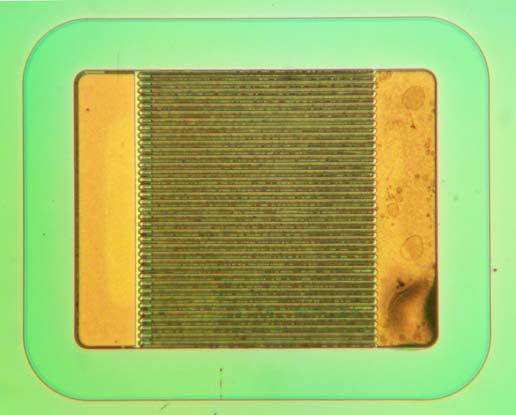
9 Fig.2 8
10 Ic (A) x1.4 mm 4H-SiC BJT (BJT#9-2, E5-37finger) Rsp,on = 2.9 mω.cm 2 β = 18.8 Active area = 0.61 mm 2 Ib=400 ma Ib=300 ma Ib=200 ma Ib=100 ma 1,000 X Ic Vceo 757 V 231 ua Jc (A/cm 2 ) Vce (V) Fig.3 9
11 Current (A) mω.cm 2 BJT Reported in this paper 4.7 mω.cm 2 BJT Reported in ICSCRM BE Voltage (V BE ) Fig.4 10
12 FIGURE CAPTIONS Fig. 1. Cross sectional view of the 4H-SiC BJT device Fig. 2. Photo of a fabricated 4H-SiC BJT. Fig. 3. I-V characteristics of the 4H-SiC BJT. Fig. 4. Forward I-V characteristics of the base-emitter junction. 11
13 References: [1] J. Zhang, J. H. Zhao, P. Alexandrov and T. Burke, Demonstration of first 9.2 KV 4H-SiC bipolar junction transistor, in IEE Electronics Letters, Vol.40, pp , [2] C.-F. Huang and J. A. Cooper, Jr., High current gain 4H-SiC NPN Bipolar Junction Transistors, IEEE Electron Device Lett., vol.24, pp , Jun [3] J. Zhang, P. Alexandrov, and J. H. Zhao, High Power(500 V-70 A) and High Gain(44-47) 4H-SiC Bipolar Junction Transistors, in Materials Science Forum, Vol , pp , [4] A. Agarwal, S. H. Ryu, C. Capell, J. Richmond, J. Palmour, H. Bartlow, P. Chow, S. Scozzie, W. Tipton, S. Baynes and K. Jones, SiC BJT technology for power switching and RF applications. in Materials Science Forum, vol , pp , [5] A. Agarwal, S. H. Ryu, J. Richmond, C. Capell, J. W. Palmar, S. Balachandran, T. P. Chow, B. Geil, S. Bayne, C. Scozzie and K. A. Jones, Recent progress in SiC bipolar junction transistors, in IEEE Int. Symp. On Power Semicondctor Devices and IC s (ISPSD) 2004, pp [6] S. Krishnaswami, A. Agarwal, C. Capell, J. Richmond, S.H. Ryu, J. Palmar, S. Balachandran, T. P. Chow, S. Bayne, B. Geil, K. A. Jones and C. Scozzie, 1000 V-30 A SiC bipolar junction transistors and integrated darlington pairs, in Materials Science Forum Vol , pp , [7] Jianhui Zhang, Petre Alexandrov, Jian H. Zhao and Terry Burke, 1677 V, 5.7 mω.cm 2 4H-SiC BJTs, in IEEE Electron Device Letters, Vol. 26, pp ,
14 [8] Anant K. Agarwal, Sumi Krishnaswami, James Richmond, Craig Capell, Sei-Hyung Ryu, John W. Palmour, Santosh Balachandran, T. Paul Chow, Stephen Bayne, Bruce Geil, Charles Scozzie and Kenneth A. Jones, Evolution of the 1600 V, 20 A, SiC bipolar junction transistors, in Proc. Of 17 th international symposium on power semiconductor devices & IC s (ISPSD), pp , [9] Sumi Krishnaswami, Anant Agarwal, James Richmond, Craig Capell, Sei-Hyung Ryu, John Palmour, Bruce Geil, Dimosthenis Katsis, and Charles Scozzie, High temperature characterization of 4H-SiC bipolar junction transistors, in ICSCRM [10] Jianhui Zhang, Jian Wu, Petre Alexandrov, Terry Burke, Kuang Sheng and Jian H. Zhao, 1836 V, 4.7 mω.cm 2 high power 4H-SiC bipolar junction transistor, in ICSCRM [11] Kiyoshi Tone and Jian H. Zhao, A comparative study of C plus Al coimplantation and Al implantation in 4H- and 6H-SiC, in IEEE Transanctions on Electron Devices, Vol. 46, No. 3, pp , [12] J. H. Zhao, J. Zhang, P. Alexandrov, X. Li, and T. Burke, A High Voltage (1,750 V) and High Current Gain (β= 24.8) 4H-SiC Bipolar Junction Transistor Using a Thin (12 μm) Drift Layer, in Materials Science Forum, Vol , pp ,
Implantation-Free 4H-SiC Bipolar Junction Transistors with Double Base Epi-layers
 Implantation-Free 4H-SiC Bipolar Junction Transistors with Double Base Epi-layers Jianhui Zhang, member, IEEE, Xueqing, Li, Petre Alexandrov, member, IEEE, Terry Burke, member, IEEE, and Jian H. Zhao,
PULSED POWER SWITCHING OF 4H-SIC VERTICAL D-MOSFET AND DEVICE CHARACTERIZATION
 PULSED POWER SWITCHING OF 4H-SIC VERTICAL D-MOSFET AND DEVICE CHARACTERIZATION Argenis Bilbao, William B. Ray II, James A. Schrock, Kevin Lawson and Stephen B. Bayne Texas Tech University, Electrical and
HIGH TEMPERATURE (250 C) SIC POWER MODULE FOR MILITARY HYBRID ELECTRICAL VEHICLE APPLICATIONS
 SIC POWER MODULE FOR MILITARY HYBRID ELECTRICAL VEHICLE APPLICATIONS") HIGH TEMPERATURE (250 C) SIC POWER MODULE FOR MILITARY HYBRID ELECTRICAL VEHICLE APPLICATIONS R. M. Schupbach, B. McPherson, T. McNutt, A. B. Lostetter John P. Kajs, and Scott G Castagno 29 July 2011 :
HIGH TEMPERATURE (250 C) SIC POWER MODULE FOR MILITARY HYBRID ELECTRICAL VEHICLE APPLICATIONS R. M. Schupbach, B. McPherson, T. McNutt, A. B. Lostetter John P. Kajs, and Scott G Castagno 29 July 2011 :
SILICON CARBIDE FOR NEXT GENERATION VEHICULAR POWER CONVERTERS. John Kajs SAIC August UNCLASSIFIED: Dist A. Approved for public release
 SILICON CARBIDE FOR NEXT GENERATION VEHICULAR POWER CONVERTERS John Kajs SAIC 18 12 August 2010 Report Documentation Page Form Approved OMB No. 0704-0188 Public reporting burden for the collection of information
Advances in SiC Power Technology
 Advances in SiC Power Technology DARPA MTO Symposium San Jose, CA March 7, 2007 John Palmour David Grider, Anant Agarwal, Brett Hull, Bob Callanan, Jon Zhang, Jim Richmond, Mrinal Das, Joe Sumakeris, Adrian
Dr.R.Seyezhai/ International Journal of Engineering Research and Applications (IJERA)
") Dr.R.Seyezhai/ International Journal of Engineering Research and Applications (IJERA) Modeling and Simulation of Silicon Carbide (SiC) Based Bipolar Junction Transistor Dr.R.Seyezhai * *Associate Professor,
Dr.R.Seyezhai/ International Journal of Engineering Research and Applications (IJERA) Modeling and Simulation of Silicon Carbide (SiC) Based Bipolar Junction Transistor Dr.R.Seyezhai * *Associate Professor,
11.72 cm 2 SiC Wafer-scale Interconnected 64 ka PiN Diode
 11.72 cm 2 SiC Wafer-scale Interconnected 64 ka PiN Diode M. Snook 1,a, H. Hearne 1, T. McNutt 2, N. El-Hinnawy 1, V. Veliadis 1, B. Nechay 1, S. Woodruff 1, R. S. Howell 1, D. Giorgi 3, J. White 4,b,
Thermal Simulation of a Silicon Carbide (SiC) Insulated-Gate Bipolar Transistor (IGBT) in Continuous Switching Mode
 Insulated-Gate Bipolar Transistor (IGBT) in Continuous Switching Mode") ARL-MR-0973 APR 2018 US Army Research Laboratory Thermal Simulation of a Silicon Carbide (SiC) Insulated-Gate Bipolar Transistor (IGBT) in Continuous Switching Mode by Gregory Ovrebo NOTICES Disclaimers
ARL-MR-0973 APR 2018 US Army Research Laboratory Thermal Simulation of a Silicon Carbide (SiC) Insulated-Gate Bipolar Transistor (IGBT) in Continuous Switching Mode by Gregory Ovrebo NOTICES Disclaimers
DEVELOPMENT OF STITCH SUPER-GTOS FOR PULSED POWER
 DEVELOPMENT OF STITCH SUPER-GTOS FOR PULSED POWER Heather O Brien, Aderinto Ogunniyi, Charles J. Scozzie U.S. Army Research Laboratory, 2800 Powder Mill Road Adelphi, MD 20783 USA William Shaheen Berkeley
NARROW AND WIDE PULSE EVALUATION OF SILICON CARBIDE SGTO MODULES
 NARROW AND WIDE PULSE EVALUATION OF SILICON CARBIDE SGTO MODULES Aderinto Ogunniyi, Heather O Brien, Charles J. Scozzie U.S. Army Research Laboratory, 2800 Powder Mill Road Adelphi, MD 20783 USA William
0.18 μm CMOS Fully Differential CTIA for a 32x16 ROIC for 3D Ladar Imaging Systems
 0.18 μm CMOS Fully Differential CTIA for a 32x16 ROIC for 3D Ladar Imaging Systems Jirar Helou Jorge Garcia Fouad Kiamilev University of Delaware Newark, DE William Lawler Army Research Laboratory Adelphi,
11.72-cm 2 Active-area Wafer Interconnected PiN Diode pulsed at 64 ka dissipates 382 J and exhibits an action of 1.7 MA 2 -s
 1 11.72-cm 2 Active-area Wafer Interconnected PiN Diode pulsed at 64 ka dissipates 382 J and exhibits an action of 1.7 MA 2 -s M. Snook, H. Hearne, T. McNutt, N. El-Hinnawy, V. Veliadis, B. Nechay, S.
Improved Performance of Silicon Carbide Detector Using Double Layer Anti Reflection (AR) Coating
 Coating") Improved Performance of Silicon Carbide Detector Using Double Layer Anti Reflection (AR) Coating by N. C. Das, A. V. Sampath, H. Shen, and M. Wraback ARL-TN-0563 August 2013 Approved for public release;
Improved Performance of Silicon Carbide Detector Using Double Layer Anti Reflection (AR) Coating by N. C. Das, A. V. Sampath, H. Shen, and M. Wraback ARL-TN-0563 August 2013 Approved for public release;
Experimental Studies of Vulnerabilities in Devices and On-Chip Protection
 Acknowledgements: Support by the AFOSR-MURI Program is gratefully acknowledged 6/8/02 Experimental Studies of Vulnerabilities in Devices and On-Chip Protection Agis A. Iliadis Electrical and Computer Engineering
Performance Comparison of Top and Bottom Contact Gallium Arsenide (GaAs) Solar Cell
 Solar Cell") Performance Comparison of Top and Bottom Contact Gallium Arsenide (GaAs) Solar Cell by Naresh C Das ARL-TR-7054 September 2014 Approved for public release; distribution unlimited. NOTICES Disclaimers The
Performance Comparison of Top and Bottom Contact Gallium Arsenide (GaAs) Solar Cell by Naresh C Das ARL-TR-7054 September 2014 Approved for public release; distribution unlimited. NOTICES Disclaimers The
QRTECH AB, Mejerigatan 1, Gothenburg, Sweden
 Materials Science Forum Online: 213-1-25 ISSN: 1662-9752, Vols. 74-742, pp 97-973 doi:1.428/www.scientific.net/msf.74-742.97 213 Trans Tech Publications, Switzerland 1 V, 3.3 m SiC bipolar junction transistor
Development of a charged-particle accumulator using an RF confinement method FA
 Development of a charged-particle accumulator using an RF confinement method FA4869-08-1-4075 Ryugo S. Hayano, University of Tokyo 1 Impact of the LHC accident This project, development of a charged-particle
ANTENNA DEVELOPMENT FOR MULTIFUNCTIONAL ARMOR APPLICATIONS USING EMBEDDED SPIN-TORQUE NANO-OSCILLATOR (STNO) AS A MICROWAVE DETECTOR
 AS A MICROWAVE DETECTOR") ANTENNA DEVELOPMENT FOR MULTIFUNCTIONAL ARMOR APPLICATIONS USING EMBEDDED SPIN-TORQUE NANO-OSCILLATOR (STNO) AS A MICROWAVE DETECTOR Report Documentation Page Form Approved OMB No. 0704-0188 Public reporting
ANTENNA DEVELOPMENT FOR MULTIFUNCTIONAL ARMOR APPLICATIONS USING EMBEDDED SPIN-TORQUE NANO-OSCILLATOR (STNO) AS A MICROWAVE DETECTOR Report Documentation Page Form Approved OMB No. 0704-0188 Public reporting
Strategic Technical Baselines for UK Nuclear Clean-up Programmes. Presented by Brian Ensor Strategy and Engineering Manager NDA
 Strategic Technical Baselines for UK Nuclear Clean-up Programmes Presented by Brian Ensor Strategy and Engineering Manager NDA Report Documentation Page Form Approved OMB No. 0704-0188 Public reporting
REPORT DOCUMENTATION PAGE
 REPORT DOCUMENTATION PAGE Form Approved OMB No. 0704-0188 Public reporting burden for this collection of information is estimated to average 1 hour per response, including the time for reviewing instructions,
Investigation of a Forward Looking Conformal Broadband Antenna for Airborne Wide Area Surveillance
 Investigation of a Forward Looking Conformal Broadband Antenna for Airborne Wide Area Surveillance Hany E. Yacoub Department Of Electrical Engineering & Computer Science 121 Link Hall, Syracuse University,
Challenges in Imaging, Sensors, and Signal Processing
 Challenges in Imaging, Sensors, and Signal Processing Raymond Balcerak MTO Technology Symposium March 5-7, 2007 1 Report Documentation Page Form Approved OMB No. 0704-0188 Public reporting burden for the
Rump Session: Advanced Silicon Technology Foundry Access Options for DoD Research. Prof. Ken Shepard. Columbia University
 Rump Session: Advanced Silicon Technology Foundry Access Options for DoD Research Prof. Ken Shepard Columbia University The views and opinions presented by the invited speakers are their own and should
9 kv, 1 cm 1 cm SiC SUPER GTO TECHNOLOGY DEVELOPMENT FOR PULSE POWER
 9 kv, 1 cm 1 cm SiC SUPER GTO TECHNOLOGY DEVELOPMENT FOR PULSE POWER A. Agarwal 1.a, C. Capell 1, Q. Zhang 1, J. Richmond 1, R. Callanan 1, M. O Loughlin 1, A. Burk 1, J. Melcher 1, J. Palmour 1, V. Temple
Fuzzy Logic Approach for Impact Source Identification in Ceramic Plates
 Fuzzy Logic Approach for Impact Source Identification in Ceramic Plates Shashank Kamthan 1, Harpreet Singh 1, Arati M. Dixit 1, Vijay Shrama 1, Thomas Reynolds 2, Ivan Wong 2, Thomas Meitzler 2 1 Dept
Nanoimprinting of micro-optical components fabricated using stamps made with Proton Beam Writing
 Nanoimprinting of micro-optical components fabricated using stamps made with Proton Beam Writing JA van Kan 1 AA Bettiol 1,T. Osipowicz 2 and F. Watt 3 1 Research fellow, 2 Deputy Director of CIBA and
Self-Aligned-Gate GaN-HEMTs with Heavily-Doped n + -GaN Ohmic Contacts to 2DEG
 Self-Aligned-Gate GaN-HEMTs with Heavily-Doped n + -GaN Ohmic Contacts to 2DEG K. Shinohara, D. Regan, A. Corrion, D. Brown, Y. Tang, J. Wong, G. Candia, A. Schmitz, H. Fung, S. Kim, and M. Micovic HRL
FY07 New Start Program Execution Strategy
 FY07 New Start Program Execution Strategy DISTRIBUTION STATEMENT D. Distribution authorized to the Department of Defense and U.S. DoD contractors strictly associated with TARDEC for the purpose of providing
Limits to the Exponential Advances in DWDM Filter Technology? Philip J. Anthony
 Limits to the Exponential Advances in DWDM Filter Technology? DARPA/MTO WDM for Military Platforms April 18-19, 2000 McLean, VA Philip J. Anthony E-TEK Dynamics San Jose CA phil.anthony@e-tek.com Report
REPORT DOCUMENTATION PAGE. Thermal transport and measurement of specific heat in artificially sculpted nanostructures. Dr. Mandar Madhokar Deshmukh
 REPORT DOCUMENTATION PAGE Form Approved OMB No. 0704-0188 The public reporting burden for this collection of information is estimated to average 1 hour per response, including the time for reviewing instructions,
Noise Tolerance of Improved Max-min Scanning Method for Phase Determination
 Noise Tolerance of Improved Max-min Scanning Method for Phase Determination Xu Ding Research Assistant Mechanical Engineering Dept., Michigan State University, East Lansing, MI, 48824, USA Gary L. Cloud,
David Siegel Masters Student University of Cincinnati. IAB 17, May 5 7, 2009 Ford & UM
 Alternator Health Monitoring For Vehicle Applications David Siegel Masters Student University of Cincinnati Report Documentation Page Form Approved OMB No. 0704-0188 Public reporting burden for the collection
Integrated diodes. The forward voltage drop only slightly depends on the forward current. ELEKTRONIKOS ĮTAISAI
 1 Integrated diodes pn junctions of transistor structures can be used as integrated diodes. The choice of the junction is limited by the considerations of switching speed and breakdown voltage. The forward
ANALYSIS OF A PULSED CORONA CIRCUIT
 ANALYSIS OF A PULSED CORONA CIRCUIT R. Korzekwa (MS-H851) and L. Rosocha (MS-E526) Los Alamos National Laboratory P.O. Box 1663, Los Alamos, NM 87545 M. Grothaus Southwest Research Institute 6220 Culebra
DEVELOPMENT OF AN ULTRA-COMPACT EXPLOSIVELY DRIVEN MAGNETIC FLUX COMPRESSION GENERATOR SYSTEM
 DEVELOPMENT OF AN ULTRA-COMPACT EXPLOSIVELY DRIVEN MAGNETIC FLUX COMPRESSION GENERATOR SYSTEM J. Krile ξ, S. Holt, and D. Hemmert HEM Technologies, 602A Broadway Lubbock, TX 79401 USA J. Walter, J. Dickens
IREAP. MURI 2001 Review. John Rodgers, T. M. Firestone,V. L. Granatstein, M. Walter
 MURI 2001 Review Experimental Study of EMP Upset Mechanisms in Analog and Digital Circuits John Rodgers, T. M. Firestone,V. L. Granatstein, M. Walter Institute for Research in Electronics and Applied Physics
High-Voltage n-channel IGBTs on Free-Standing 4H-SiC Epilayers
 Purdue University Purdue e-pubs Birck and NCN Publications Birck Nanotechnology Center 2-2010 High-Voltage n-channel IGBTs on Free-Standing 4H-SiC Epilayers Xiaokun Wang Purdue University - Main Campus
Development of SiC BJT based PWM Inverter for renewable energy resources
 International Journal of Scientific & Engineering Research, Volume 2, Issue 11, November-2011 1 Development of SiC BJT based PWM Inverter for renewable energy resources Dr.R.Seyezhai Abstract - Silicon
Static and Dynamic Characterization of High-Speed Silicon Carbide (SiC) Power Transistors
 Power Transistors") Engineering, 21, 2, 673-682 doi:1.4236/eng.21.2987 Published Online September 21 (http://www.scirp.org/journal/eng) Static and Dynamic Characterization of High-Speed Silicon Carbide (SiC) Power Transistors
Engineering, 21, 2, 673-682 doi:1.4236/eng.21.2987 Published Online September 21 (http://www.scirp.org/journal/eng) Static and Dynamic Characterization of High-Speed Silicon Carbide (SiC) Power Transistors
Experiences Linking Vehicle Motion Simulators to Distributed Simulation Experiments
 Experiences Linking Vehicle Motion Simulators to Distributed Simulation Experiments Richard W. Jacobson Electrical Engineer 1/ 18 Report Documentation Page Form Approved OMB No. 0704-0188 Public reporting
COM DEV AIS Initiative. TEXAS II Meeting September 03, 2008 Ian D Souza
 COM DEV AIS Initiative TEXAS II Meeting September 03, 2008 Ian D Souza 1 Report Documentation Page Form Approved OMB No. 0704-0188 Public reporting burden for the collection of information is estimated
INVESTIGATION OF A HIGH VOLTAGE, HIGH FREQUENCY POWER CONDITIONING SYSTEM FOR USE WITH FLUX COMPRESSION GENERATORS
 INVESTIGATION OF A HIGH VOLTAGE, HIGH FREQUENCY POWER CONDITIONING SYSTEM FOR USE WITH FLUX COMPRESSION GENERATORS K. A. O Connor ξ and R. D. Curry University of Missouri-Columbia, 349 Engineering Bldg.
DIELECTRIC ROTMAN LENS ALTERNATIVES FOR BROADBAND MULTIPLE BEAM ANTENNAS IN MULTI-FUNCTION RF APPLICATIONS. O. Kilic U.S. Army Research Laboratory
 DIELECTRIC ROTMAN LENS ALTERNATIVES FOR BROADBAND MULTIPLE BEAM ANTENNAS IN MULTI-FUNCTION RF APPLICATIONS O. Kilic U.S. Army Research Laboratory ABSTRACT The U.S. Army Research Laboratory (ARL) is currently
Analytical Study of Tunable Bilayered-Graphene Dipole Antenna
 1 Analytical Study of Tunable Bilayered-Graphene Dipole Antenna James E. Burke RDAR-MEF-S, bldg. 94 1 st floor Sensor & Seekers Branch/MS&G Division/FPAT Directorate U.S. RDECOM-ARDEC, Picatinny Arsenal,
Key Issues in Modulating Retroreflector Technology
 Key Issues in Modulating Retroreflector Technology Dr. G. Charmaine Gilbreath, Code 7120 Naval Research Laboratory 4555 Overlook Ave., NW Washington, DC 20375 phone: (202) 767-0170 fax: (202) 404-8894
Thermal Simulation of Switching Pulses in an Insulated Gate Bipolar Transistor (IGBT) Power Module
 Power Module") Thermal Simulation of Switching Pulses in an Insulated Gate Bipolar Transistor (IGBT) Power Module by Gregory K Ovrebo ARL-TR-7210 February 2015 Approved for public release; distribution unlimited. NOTICES
Thermal Simulation of Switching Pulses in an Insulated Gate Bipolar Transistor (IGBT) Power Module by Gregory K Ovrebo ARL-TR-7210 February 2015 Approved for public release; distribution unlimited. NOTICES
Study on Fabrication and Fast Switching of High Voltage SiC JFET
 Advanced Materials Research Online: 2013-10-31 ISSN: 1662-8985, Vol. 827, pp 282-286 doi:10.4028/www.scientific.net/amr.827.282 2014 Trans Tech Publications, Switzerland Study on Fabrication and Fast Switching
ARL-TN-0743 MAR US Army Research Laboratory
 ARL-TN-0743 MAR 2016 US Army Research Laboratory Microwave Integrated Circuit Amplifier Designs Submitted to Qorvo for Fabrication with 0.09-µm High-Electron-Mobility Transistors (HEMTs) Using 2-mil Gallium
Joint Milli-Arcsecond Pathfinder Survey (JMAPS): Overview and Application to NWO Mission
: Overview and Application to NWO Mission") Joint Milli-Arcsecond Pathfinder Survey (JMAPS): Overview and Application to NWO Mission B.DorlandandR.Dudik USNavalObservatory 11March2009 1 MissionOverview TheJointMilli ArcsecondPathfinderSurvey(JMAPS)missionisaDepartmentof
Joint Milli-Arcsecond Pathfinder Survey (JMAPS): Overview and Application to NWO Mission B.DorlandandR.Dudik USNavalObservatory 11March2009 1 MissionOverview TheJointMilli ArcsecondPathfinderSurvey(JMAPS)missionisaDepartmentof
Lattice Spacing Effect on Scan Loss for Bat-Wing Phased Array Antennas
 Lattice Spacing Effect on Scan Loss for Bat-Wing Phased Array Antennas I. Introduction Thinh Q. Ho*, Charles A. Hewett, Lilton N. Hunt SSCSD 2825, San Diego, CA 92152 Thomas G. Ready NAVSEA PMS500, Washington,
INTEGRATIVE MIGRATORY BIRD MANAGEMENT ON MILITARY BASES: THE ROLE OF RADAR ORNITHOLOGY
 INTEGRATIVE MIGRATORY BIRD MANAGEMENT ON MILITARY BASES: THE ROLE OF RADAR ORNITHOLOGY Sidney A. Gauthreaux, Jr. and Carroll G. Belser Department of Biological Sciences Clemson University Clemson, SC 29634-0314
TRANSMISSION LINE AND ELECTROMAGNETIC MODELS OF THE MYKONOS-2 ACCELERATOR*
 TRANSMISSION LINE AND ELECTROMAGNETIC MODELS OF THE MYKONOS-2 ACCELERATOR* E. A. Madrid ξ, C. L. Miller, D. V. Rose, D. R. Welch, R. E. Clark, C. B. Mostrom Voss Scientific W. A. Stygar, M. E. Savage Sandia
SILICON DIODE EVALUATED AS RECTIFIER FOR WIDE-PULSE SWITCHING APPLICATIONS
 SILICON DIODE EVALUATED AS RECTIFIER FOR WIDE-PULSE SWITCHING APPLICATIONS Heather O Brien, Aderinto Ogunniyi, Charles J. Scozzie U.S. Army Research Laboratory, 2800 Powder Mill Road Adelphi, MD 20783
REPORT DOCUMENTATION PAGE
 REPORT DOCUMENTATION PAGE Form Approved OMB NO. 0704-0188 The public reporting burden for this collection of information is estimated to average 1 hour per response, including the time for reviewing instructions,
A 1-kV 4H-SiC power DMOSFET optimized for low ON-resistance
 Purdue University Purdue e-pubs Birck and NCN Publications Birck Nanotechnology Center October 2007 A 1-kV 4H-SiC power DMOSFET optimized for low ON-resistance Asmita Saha Purdue University James A. Cooper
DARPA TRUST in IC s Effort. Dr. Dean Collins Deputy Director, MTO 7 March 2007
 DARPA TRUST in IC s Effort Dr. Dean Collins Deputy Director, MTO 7 March 27 Report Documentation Page Form Approved OMB No. 74-88 Public reporting burden for the collection of information is estimated
Frequency Dependent Harmonic Powers in a Modified Uni-Traveling Carrier (MUTC) Photodetector
 Photodetector") Naval Research Laboratory Washington, DC 2375-532 NRL/MR/5651--17-9712 Frequency Dependent Harmonic Powers in a Modified Uni-Traveling Carrier (MUTC) Photodetector Yue Hu University of Maryland Baltimore,
Naval Research Laboratory Washington, DC 2375-532 NRL/MR/5651--17-9712 Frequency Dependent Harmonic Powers in a Modified Uni-Traveling Carrier (MUTC) Photodetector Yue Hu University of Maryland Baltimore,
PULSED BREAKDOWN CHARACTERISTICS OF HELIUM IN PARTIAL VACUUM IN KHZ RANGE
 PULSED BREAKDOWN CHARACTERISTICS OF HELIUM IN PARTIAL VACUUM IN KHZ RANGE K. Koppisetty ξ, H. Kirkici Auburn University, Auburn, Auburn, AL, USA D. L. Schweickart Air Force Research Laboratory, Wright
Department of Electrical Engineering IIT Madras
 Department of Electrical Engineering IIT Madras Sample Questions on Semiconductor Devices EE3 applicants who are interested to pursue their research in microelectronics devices area (fabrication and/or
Wavelet Shrinkage and Denoising. Brian Dadson & Lynette Obiero Summer 2009 Undergraduate Research Supported by NSF through MAA
 Wavelet Shrinkage and Denoising Brian Dadson & Lynette Obiero Summer 2009 Undergraduate Research Supported by NSF through MAA Report Documentation Page Form Approved OMB No. 0704-0188 Public reporting
Capacitive Discharge Circuit for Surge Current Evaluation of SiC
 Capacitive Discharge Circuit for Surge Current Evaluation of SiC by Mark R. Morgenstern ARL-TN-0376 November 2009 Approved for public release; distribution unlimited. NOTICES Disclaimers The findings in
Active Denial Array. Directed Energy. Technology, Modeling, and Assessment
 Directed Energy Technology, Modeling, and Assessment Active Denial Array By Randy Woods and Matthew Ketner 70 Active Denial Technology (ADT) which encompasses the use of millimeter waves as a directed-energy,
IB2-1 HIGH AVERAGE POWER TESTS OF A CROSSED-FIELD CLOSING SWITCH>:< Robin J. Harvey and Robert W. Holly
 HIGH AVERAGE POWER TESTS OF A CROSSED-FIELD CLOSING SWITCH>:< by Robin J. Harvey and Robert W. Holly Hughes Research Laboratories 3011 Malibu Canyon Road Malibu, California 90265 and John E. Creedon U.S.
OPTICAL EMISSION CHARACTERISTICS OF HELIUM BREAKDOWN AT PARTIAL VACUUM FOR POINT TO PLANE GEOMETRY
 OPTICAL EMISSION CHARACTERISTICS OF HELIUM BREAKDOWN AT PARTIAL VACUUM FOR POINT TO PLANE GEOMETRY K. Koppisetty ξ, H. Kirkici 1, D. L. Schweickart 2 1 Auburn University, Auburn, Alabama 36849, USA, 2
U.S. Army Training and Doctrine Command (TRADOC) Virtual World Project
 Virtual World Project") U.S. Army Research, Development and Engineering Command U.S. Army Training and Doctrine Command (TRADOC) Virtual World Project Advanced Distributed Learning Co-Laboratory ImplementationFest 2010 12 August
U.S. Army Research, Development and Engineering Command U.S. Army Training and Doctrine Command (TRADOC) Virtual World Project Advanced Distributed Learning Co-Laboratory ImplementationFest 2010 12 August
M?k^iMMIBiiS^^^M^^Ä^^^ÄÄ^I^^^ÄyM»ÄM^SSSäSä^^iB^S^«SI^M^^«^B^^^^^» ANNUAL REPORT. Novel SiC High Power IC
 M?k^iMMIBiiS^^^M^^Ä^^^ÄÄ^I^^^ÄyM»ÄM^SSSäSä^^iB^S^«SI^M^^«^B^^^^^» ANNUAL REPORT Novel SiC High Power IC Tehnology Supported Under Grant # N00014-98-1-0534 Office of Naval Research Funded by DARPA/ETO Program
Technology Maturation Planning for the Autonomous Approach and Landing Capability (AALC) Program
 Program") Technology Maturation Planning for the Autonomous Approach and Landing Capability (AALC) Program AFRL 2008 Technology Maturity Conference Multi-Dimensional Assessment of Technology Maturity 9-12 September
Technology Maturation Planning for the Autonomous Approach and Landing Capability (AALC) Program AFRL 2008 Technology Maturity Conference Multi-Dimensional Assessment of Technology Maturity 9-12 September
FLASH X-RAY (FXR) ACCELERATOR OPTIMIZATION BEAM-INDUCED VOLTAGE SIMULATION AND TDR MEASUREMENTS *
 ACCELERATOR OPTIMIZATION BEAM-INDUCED VOLTAGE SIMULATION AND TDR MEASUREMENTS *") FLASH X-RAY (FXR) ACCELERATOR OPTIMIZATION BEAM-INDUCED VOLTAGE SIMULATION AND TDR MEASUREMENTS * Mike M. Ong and George E. Vogtlin Lawrence Livermore National Laboratory, PO Box 88, L-13 Livermore, CA,
FLASH X-RAY (FXR) ACCELERATOR OPTIMIZATION BEAM-INDUCED VOLTAGE SIMULATION AND TDR MEASUREMENTS * Mike M. Ong and George E. Vogtlin Lawrence Livermore National Laboratory, PO Box 88, L-13 Livermore, CA,
August 9, Attached please find the progress report for ONR Contract N C-0230 for the period of January 20, 2015 to April 19, 2015.
 August 9, 2015 Dr. Robert Headrick ONR Code: 332 O ce of Naval Research 875 North Randolph Street Arlington, VA 22203-1995 Dear Dr. Headrick, Attached please find the progress report for ONR Contract N00014-14-C-0230
Loop-Dipole Antenna Modeling using the FEKO code
 Loop-Dipole Antenna Modeling using the FEKO code Wendy L. Lippincott* Thomas Pickard Randy Nichols lippincott@nrl.navy.mil, Naval Research Lab., Code 8122, Wash., DC 237 ABSTRACT A study was done to optimize
Digital Radiography and X-ray Computed Tomography Slice Inspection of an Aluminum Truss Section
 Digital Radiography and X-ray Computed Tomography Slice Inspection of an Aluminum Truss Section by William H. Green ARL-MR-791 September 2011 Approved for public release; distribution unlimited. NOTICES
Durable Aircraft. February 7, 2011
 Durable Aircraft February 7, 2011 Report Documentation Page Form Approved OMB No. 0704-0188 Public reporting burden for the collection of information is estimated to average 1 hour per response, including
VHF/UHF Imagery of Targets, Decoys, and Trees
 F/UHF Imagery of Targets, Decoys, and Trees A. J. Gatesman, C. Beaudoin, R. Giles, J. Waldman Submillimeter-Wave Technology Laboratory University of Massachusetts Lowell J.L. Poirier, K.-H. Ding, P. Franchi,
Signal Processing Architectures for Ultra-Wideband Wide-Angle Synthetic Aperture Radar Applications
 Signal Processing Architectures for Ultra-Wideband Wide-Angle Synthetic Aperture Radar Applications Atindra Mitra Joe Germann John Nehrbass AFRL/SNRR SKY Computers ASC/HPC High Performance Embedded Computing
Frequency Stabilization Using Matched Fabry-Perots as References
 April 1991 LIDS-P-2032 Frequency Stabilization Using Matched s as References Peter C. Li and Pierre A. Humblet Massachusetts Institute of Technology Laboratory for Information and Decision Systems Cambridge,
A RENEWED SPIRIT OF DISCOVERY
 A RENEWED SPIRIT OF DISCOVERY The President s Vision for U.S. Space Exploration PRESIDENT GEORGE W. BUSH JANUARY 2004 Report Documentation Page Form Approved OMB No. 0704-0188 Public reporting burden for
FAA Research and Development Efforts in SHM
 FAA Research and Development Efforts in SHM P. SWINDELL and D. P. ROACH ABSTRACT SHM systems are being developed using networks of sensors for the continuous monitoring, inspection and damage detection
Nanosecond Thermal Processing for Self-Aligned Silicon-on-Insulator Technology
 TECHNICAL DOCUMENT 3195 April 2005 Nanosecond Thermal Processing for Self-Aligned Silicon-on-Insulator Technology A. D. Ramirez B. W. Offord J. D. Popp S. D. Russell J. F. Rowland Approved for public release;
Tom Cat Designs LLC Protective Hull Modeling & Simulation Results For Iteration 1
 Tom Cat Designs LLC Protective Hull Modeling & Simulation Results For Iteration 1 Sebastian Karwaczynski 24- October- 2011 DISTRIBUTION STATEMENT A. Approved for public release; distribution is unlimited.
ARL-TN-0835 July US Army Research Laboratory
 ARL-TN-0835 July 2017 US Army Research Laboratory Gallium Nitride (GaN) Monolithic Microwave Integrated Circuit (MMIC) Designs Submitted to Air Force Research Laboratory (AFRL)- Sponsored Qorvo Fabrication
14. Model Based Systems Engineering: Issues of application to Soft Systems
 DSTO-GD-0734 14. Model Based Systems Engineering: Issues of application to Soft Systems Ady James, Alan Smith and Michael Emes UCL Centre for Systems Engineering, Mullard Space Science Laboratory Abstract
CHARACTERIZATION OF PASCHEN CURVE ANOMOLIES AT HIGH P*D VALUES
 CHARACTERIZATION OF PASCHEN CURVE ANOMOLIES AT HIGH P*D VALUES W.J. Carey, A.J. Wiebe, R.D. Nord ARC Technology, 1376 NW 12 th St. Whitewater, Kansas, USA L.L. Altgilbers (Senior Member) US Army Space
Innovative 3D Visualization of Electro-optic Data for MCM
 Innovative 3D Visualization of Electro-optic Data for MCM James C. Luby, Ph.D., Applied Physics Laboratory University of Washington 1013 NE 40 th Street Seattle, Washington 98105-6698 Telephone: 206-543-6854
REPORT DOCUMENTATION PAGE
 REPORT DOCUMENTATION PAGE Form Approved OMB No. 0704-0188 Public reporting burden for this collection of information is estimated to average 1 hour per response, including the time for reviewing instructions,
Ultrasonic Nonlinearity Parameter Analysis Technique for Remaining Life Prediction
 Ultrasonic Nonlinearity Parameter Analysis Technique for Remaining Life Prediction by Raymond E Brennan ARL-TN-0636 September 2014 Approved for public release; distribution is unlimited. NOTICES Disclaimers
[Research Title]: Electro-spun fine fibers of shape memory polymer used as an engineering part. Contractor (PI): Hirohisa Tamagawa
![[Research Title]: Electro-spun fine fibers of shape memory polymer used as an engineering part. Contractor (PI): Hirohisa Tamagawa](/thumbs/72/67640784.jpg "[Research Title]: Electro-spun fine fibers of shape memory polymer used as an engineering part. Contractor (PI): Hirohisa Tamagawa") [Research Title]: Electro-spun fine fibers of shape memory polymer used as an engineering part Contractor (PI): Hirohisa Tamagawa WORK Information: Organization Name: Gifu University Organization Address:
[Research Title]: Electro-spun fine fibers of shape memory polymer used as an engineering part Contractor (PI): Hirohisa Tamagawa WORK Information: Organization Name: Gifu University Organization Address:
MULTI-KILOVOLT SOLID-STATE PICOSECOND SWITCH STUDIES *
 MULTI-KILOVOLT SOLID-STATE PICOSECOND SWITCH STUDIES * C. A. Frost, R. J. Focia, and T. C. Stockebrand Pulse Power Physics, Inc. 139 Red Oaks Loop NE Albuquerque, NM 87122 M. J. Walker and J. Gaudet Air
EFFECTS OF ELECTROMAGNETIC PULSES ON A MULTILAYERED SYSTEM
 EFFECTS OF ELECTROMAGNETIC PULSES ON A MULTILAYERED SYSTEM A. Upia, K. M. Burke, J. L. Zirnheld Energy Systems Institute, Department of Electrical Engineering, University at Buffalo, 230 Davis Hall, Buffalo,
SA Joint USN/USMC Spectrum Conference. Gerry Fitzgerald. Organization: G036 Project: 0710V250-A1
 SA2 101 Joint USN/USMC Spectrum Conference Gerry Fitzgerald 04 MAR 2010 DISTRIBUTION A: Approved for public release Case 10-0907 Organization: G036 Project: 0710V250-A1 Report Documentation Page Form Approved
Basic Studies in Microwave Sciences FA
 Basic Studies in Microwave Sciences FA9550 06 1 0505 Final Report Principal Investigator: Dr. Pingshan Wang Institution: Clemson University Address: 215 Riggs Hall, Clemson SC 29634 1 REPORT DOCUMENTATION
Evaluation of Bidirectional Silicon Carbide Solid-State Circuit Breaker v3.2
 Evaluation of Bidirectional Silicon Carbide Solid-State Circuit Breaker v3.2 by D. Urciuoli ARL-MR-0845 July 2013 Approved for public release; distribution unlimited. NOTICES Disclaimers The findings in
Robotics and Artificial Intelligence. Rodney Brooks Director, MIT Computer Science and Artificial Intelligence Laboratory CTO, irobot Corp
 Robotics and Artificial Intelligence Rodney Brooks Director, MIT Computer Science and Artificial Intelligence Laboratory CTO, irobot Corp Report Documentation Page Form Approved OMB No. 0704-0188 Public
Student Independent Research Project : Evaluation of Thermal Voltage Converters Low-Frequency Errors
 . Session 2259 Student Independent Research Project : Evaluation of Thermal Voltage Converters Low-Frequency Errors Svetlana Avramov-Zamurovic and Roger Ashworth United States Naval Academy Weapons and
Feasibility of T/R Module Functionality in a Single SiGe IC
 Feasibility of T/R Module Functionality in a Single SiGe IC Dr. John D. Cressler, Jonathan Comeau, Joel Andrews, Lance Kuo, Matt Morton, and Dr. John Papapolymerou Georgia Institute of Technology Georgia
RECENT TIMING ACTIVITIES AT THE U.S. NAVAL RESEARCH LABORATORY
 RECENT TIMING ACTIVITIES AT THE U.S. NAVAL RESEARCH LABORATORY Ronald Beard, Jay Oaks, Ken Senior, and Joe White U.S. Naval Research Laboratory 4555 Overlook Ave. SW, Washington DC 20375-5320, USA Abstract
Radar Detection of Marine Mammals
 DISTRIBUTION STATEMENT A. Approved for public release; distribution is unlimited. Radar Detection of Marine Mammals Charles P. Forsyth Areté Associates 1550 Crystal Drive, Suite 703 Arlington, VA 22202
Thermal Simulation of a Diode Module Cooled with Forced Convection
 Thermal Simulation of a Diode Module Cooled with Forced Convection by Gregory K. Ovrebo ARL-MR-0787 July 2011 Approved for public release; distribution unlimited. NOTICES Disclaimers The findings in this
Gallium nitride (GaN)
") 80 Technology focus: GaN power electronics Vertical, CMOS and dual-gate approaches to gallium nitride power electronics US research company HRL Laboratories has published a number of papers concerning
80 Technology focus: GaN power electronics Vertical, CMOS and dual-gate approaches to gallium nitride power electronics US research company HRL Laboratories has published a number of papers concerning
PHASING CAPABILITY. Abstract ARRAY. level. up to. to 12 GW. device s outpu antenna array. Electric Mode. same physical dimensions.
 PULSED HIGHH POWER MICROWAVE ( HPM) OSCILLATOR WITH PHASING CAPABILITY V A. Somov, Yu. Tkach Institute For Electromagneticc Research Ltd., Pr. Pravdi 5, Kharkiv 61022, Ukraine, S.A.Mironenko State Foreign
Evanescent Acoustic Wave Scattering by Targets and Diffraction by Ripples
 Evanescent Acoustic Wave Scattering by Targets and Diffraction by Ripples PI name: Philip L. Marston Physics Department, Washington State University, Pullman, WA 99164-2814 Phone: (509) 335-5343 Fax: (509)