ECEN720: High-Speed Links Circuits and Systems Spring 2017
|
|
|
- Joseph Garrison
- 6 years ago
- Views:
Transcription


1 ECEN720: High-Speed Links Circuits and Systems Spring 2017 Lecture 9: Noise Sources Sam Palermo Analog & Mixed-Signal Center Texas A&M University
2 Announcements Lab 5 Report and Prelab 6 due Apr. 3 Stateye theory paper posted on website 2
![Noise in High-Speed Link Systems [Dally] Multiple](/docs-images/74/69882945/images/3-0.jpg "noise sources can degrade link timing and amplitude")
3 Noise in High-Speed Link Systems [Dally] Multiple noise sources can degrade link timing and amplitude margin 3
4 Noise Source Overview Common noise sources Power supply noise Receiver offset Crosstalk Inter-symbol interference Random noise Power supply noise Switching current through finite supply impedance causes supply voltage drops that vary with time and physical location Receiver offset Caused by random device mismatches Crosstalk One signal (aggressor) interfering with another signal (victim) On-chip coupling (capacitive) Off-chip coupling (t-line) Near-end Far-end Inter-symbol interference Signal dispersion causes signal to interfere with itself Random noise Thermal & shot noise Clock jitter components 4
5 Bounded and Statistical Noise Sources Bounded or deterministic Statistical or random noise noise sources sources Have theoretically predictable values with defined worst-case bounds Allows for simple (but pessimistic) worst-case analysis Examples Crosstalk to small channel count ISI Receiver offset Treat noise as a random process Source may be psuedo-random Often characterized w/ Gaussian stats RMS value Probability density function (PDF) Examples Thermal noise Clock jitter components Crosstalk to large channel count Understanding whether noise source is bounded or random is critical to accurate link performance estimation 5
6 Proportional and Independent Noise Sources Some noise is proportional to signal swing Crosstalk Simultaneous switching power supply noise ISI Can t overpower this noise Larger signal = more noise Some noise is independent to signal swing RX offset Non-IO power supply noise Can overpower this noise Total noise V N K N V S V NI Independent noise Proportional noise constant Signal swing 6
7 Common Noise Sources Power supply noise Receiver offset Crosstalk Inter-symbol interference Random noise 7
8 Power Supply Noise [Hodges] Circuits draw current from the VDD supply nets and return current to the GND nets Supply networks have finite impedance Time-varying (switching) currents induce variations on the supply voltage Supply noise a circuit sees depends on its location in supply distribution network 8


9 Power Routing Bad Block B will experience excessive supply noise Better Block B will experience 1/2 supply noise, but at the cost of double the power routing through blocks Even Better Block A & B will experience similar supply noise Best Block A & B are more isolated [Hodges] [Hodges] 9
10 Supply Induced Delay Variation Supply noise can induce variations in circuit delay Results in deterministic jitter on clocks & data signals t PHL C L VDD 2 CL VDD 2 CLVDD 2 I DSATN W v C VDD V 2W NvsatCoxVDD VTN N sat ox VDD VTN E VDD Delay VDD V CN TN TN L N VDD CMOS delay is approximately directly proportional to VDD More delay results in more deterministic jitter [Hodges] 10
11 Simultaneous Switching Noise Finite supply impedance causes significant Simultaneous Switching Output (SSO) noise (xtalk) SSO noise is proportional to number of outputs switching, n, and inversely proportional to signal transition time, t r V N L i t r n LV Z t 0 s r 11
12 Common Noise Sources Power supply noise Receiver offset Crosstalk Inter-symbol interference Random noise 12
13 Receiver Input Referred Offset The input referred offset is primarily a function of V th mismatch and a weaker function of (mobility) mismatch V t AV t /, WL A WL 13
14 Receiver Input Referred Offset V t AV t, / WL A WL To reduce input offset 2x, we need to increase area 4x Not practical due to excessive area and power consumption Offset correction necessary to efficiently achieve good sensitivity Ideally the offset A coefficients are given by the design kit and Monte Carlo is performed to extract offset sigma If not, here are some common values: A Vt = 1mVm per nm of t ox For our default 90nm technology, t ox =2.8nm A Vt ~2.8mVm A is generally near 2%m 14
15 Common Noise Sources Power supply noise Receiver offset Crosstalk Inter-symbol interference Random noise 15
16 Crosstalk Crosstalk is noise induced by one signal (aggressor) that interferes with another signal (victim) Main crosstalk sources Coupling between on-chip (capacitive) wires Coupling between off-chip (t-line/channel) wires Signal return coupling Crosstalk is a proportional noise source Cannot be reduced by scaling signal levels Addressed by using proper signal conventions, improving channel and supply network, and using good circuit design and layout techniques 16
17 Crosstalk to Capacitive Lines On-chip wires have significant capacitance to adjacent wires both on same metal layer and adjacent vertical layers Floating victim Examples: Sample-nodes, domino logic When aggressor switches Signal gets coupled to victim via a capacitive voltage divider Signal is not restored [Dally] V k c B C k C c V CC C A O 17
18 Crosstalk to Driven Capacitive Lines Crosstalk to a driven line will decay away with a time-constant xc O R C C C O [Dally] Peak crosstalk is inversely proportional to aggressor transition times, t r, and driver strength (1/R O ) V B t k t V B t kc exp xc Step with Finite Rise Time, t c tr xc Ideal Unit Step : xc t k c 1 exp tr xc t t r t exp exp xc r xc : if if t t t t r r 18
19 Capacitive Crosstalk Delay Impact Aggressor transitioning near victim transition can modulate the victim s effective load capacitance This modulates the victim signal s delay, resulting in deterministic jitter [Hodges] Aggressor Static : Aggressor Switching Same Way : Aggressor Switching Opposite Way : C C L L C C L C gnd C gnd C gnd C 2C C 19
20 Mitigating Capacitive (On-Chip) Crosstalk Adjacent vertical metal layers should be routed perpendicular (Manhattan routing) Limit maximum parallel routing distance Avoid floating signals and use keeper transistors with dynamic logic Maximize signal transition time Trade-off with jitter sensitivity For differential signals, periodically twist routing to make cross-talk common-mode Separate sensitive signals Use shield wires Couple DC signals to appropriate supply 20
21 Transmission Line Crosstalk 2 coupled lines: I A I B [Dally] Transient voltage signal on A is coupled to B capacitively dv dt x, t dv x t B A k, cx dt where k cx C S CC C Capacitive coupling sends half the coupled energy in each direction with equal polarity C 21
22 Transmission Line Crosstalk 2 coupled lines: I A I B [Dally] Transient current signal on A is coupled to B through mutual inductance dvb dx x, t V x, t x, t di x, t M dv x, t dv x, t M I A A t dt L A Lx A dx k lx A dx where k lx Inductive coupling sends half the coupled energy in each direction with a negative forward traveling wave and a positive reverse traveling wave M L 22
23 Near- and Far-End Crosstalk [Hall] Near-end crosstalk (NEXT) is immediately observed starting at the aggressor transition time and continuing for a round-trip delay Due to the capacitive and inductive coupling terms having the same polarity, the NEXT signal will have the same polarity as the aggressor Far-end crosstalk (FEXT) propagates along the victim channel with the incident signal and is only observed once Due to the capacitive and inductive coupling terms having the opposite polarity, the FEXT signal can have the either polarity, and in a homogeneous medium (stripline) cancel out 23
24 Near- and Far-End Crosstalk Reverse Coupling Coefficient k rx (NEXT) t x Forward Coupling Coefficient k fx (FEXT) [Dally] k k k k rx fx k cx cx 4 k 2 lx lx For derivation of k rx and k fx, see Dally

25 Off-Chip Crosstalk Occurs mostly in package and boardto-board connectors FEXT is attenuated by channel response and has band-pass characteristic NEXT directly couples into victim and has high-pass characteristic 25
26 Signal Return Crosstalk Shared return path with finite impedance Return currents induce crosstalk occurs among signals V -V xr [Dally] Return Crosstalk Voltage : V xr V Z Z R 0 k xr V 26
27 Common Noise Sources Power supply noise Receiver offset Crosstalk Inter-symbol interference Random noise 27
28 Inter-Symbol Interference (ISI) Previous bits residual state can distort the current bit, resulting in inter-symbol interference (ISI) cursor y d k t c d t ht k post-cursor ISI pre-cursor ISI y (1) (t) sampled relative to pulse peak: [ ] k =[ ] By Linearity: y (0) (t) =-1*y (1) (t) 28
29 Peak Distortion Analysis Example s k k 0 k k 0 y (1) 0 t t kt y tkt y y 0 1 t kt y tkt t

30 Worst-Case Eye vs Random Data Eye Worst-Case Eye 100 Random Bits 1000 Random Bits 1e4 Random Bits Worst-case data pattern can occur at very low probability! Considering worst-case is too pessimistic 30
31 Constructing ISI Probability Density Function (PDF) Using ISI probability density function will yield a more accurate BER performance estimate In order to construct the total ISI PDF, need to convolve all of the individual ISI term PDFs together 50% probability of 1 symbol ISI and -1 symbol ISI 31
32 Convolving Individual ISI PDFs Together * = * = Keep going until all individual PDFs convolved together 32
33 Complete ISI PDF 33
34 Cursor PDF Data 1 * = Data 1 PDF is centered about the cursor value and varies from a maximum positive value to the worst-case value predicted by PDA This worst-case value occurs at a low probability! 34
35 Cursor Cumulative Distribution Function (CDF) For a given offset, what is the probability of a Data 1 error? Data 1 error probability for a given offset is equal to the Data 1 CDF BER X X PDF dx 35

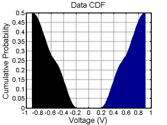
36 Combining Cursor CDFs 36

37 Bit-Error-Rate (BER) Distribution Eye Statistical BER analysis tools use this technique to account for ISI distribution and also other noise sources Example from Stateye Note: Different channel & data rate from previous slides 37
38 Common Noise Sources Power supply noise Receiver offset Crosstalk Inter-symbol interference Random noise 38
39 Random Noise Random noise is unbounded and modeled statistically Example: Circuit thermal and shot noise Modeled as a continuous random variable described by Probability density function (PDF) Mean, Standard deviation, PDF P n 2 2 x, xp x dx, x P xdx n n n n n 39

40 Gaussian Distribution Gaussian distribution is normally assumed for random noise Larger sigma value results in increased distribution spread P n x x 1 2 e 2 n


41 Signal with Added Gaussian Noise Finite probability of noise pushing signal past threshold to yield an error 41
42 Cumulative Distribution Function (CDF) The CDF tells what is the probability that the noise signal is less than or equal to a certain value n x x P n u u du x u un e 2 2 du [Dally] 42
43 Error and Complimentary Error Functions Error Function: erf x 2 2 x exp u u0 du Relationship between normal CDF (0,1) and Error Function: x 1 1 erf x 2 2 The complementary error function gives the probability that the noise will exceed a given value Q x 1 2 Q x x erfc 2 1 x erfc 1 erf x 2 x 2 43
44 Bit Error Rate (BER) Using erfc to predict BER: w/ Normal (0,1) PDF Conservative Upper-Bound Approximation [Dally] Need a symbol of about 7 for BER=10-12 Peak-to-peak value will be 2x this 44
45 Noise Source Classifications Determining whether noise source is Proportional vs Independent Bounded vs Statistical is important in noise budgeting 45

46 Noise Budget Example Peak TX differential swing of 400mV ppd equalized down 10dB 200mV 63mV Parameter K n RMS Value (BER=10-12 ) 31mV +63mV Peak Differential Swing 0.4V RX Offset + Sensitivity 5mV Power Supply Noise 5mV Residual ISI mV 31mV -63mV Crosstalk mV Random Noise 1mV 14mV Attenuation 10dB = V Total Noise 0.338V Differential Eye Height Margin 62mV Conservative analysis Assumes all distributions combine at worst-case Better technique is to use statistical BER link simulators 46
47 Next Time Timing Noise BER Analysis Techniques 47
ECEN689: Special Topics in High-Speed Links Circuits and Systems Spring 2010
 EEN689: Special Topics in High-Speed Lins ircuits and Systems Spring 2010 Lecture 21: rosstal Sam Palermo Analog & Mixed-Signal enter Texas A&M University Announcements HW6 will be posted today and due
High-speed Serial Interface
 High-speed Serial Interface Lect. 9 Noises 1 Block diagram Where are we today? Serializer Tx Driver Channel Rx Equalizer Sampler Deserializer PLL Clock Recovery Tx Rx 2 Sampling in Rx Interface applications
EE273 Lecture 5 Noise Part 2 Signal Return Crosstalk, Inter-Symbol Interference, Managing Noise
 Copyright 2004 by WJD and HCB, all rights reserved. 1 EE273 Lecture 5 Noise Part 2 Signal Return Crosstalk, Inter-Symbol Interference, Managing Noise January 26, 2004 Heinz Blennemann Stanford University
EE273 Lecture 6 Signal Return Crosstalk, Inter-Symbol Interference, Managing Noise. Today s Assignment
 EE273 Lecture 6 Signal Return Crosstalk, Inter-Symbol Interference, Managing Noise October 12, 1998 William J. Dally Computer Systems Laboratory Stanford University billd@csl.stanford.edu 1 Today s Assignment
ECEN689: Special Topics in High-Speed Links Circuits and Systems Spring 2012
 ECEN689: Special Topics in High-Speed Links Circuits and Systems Spring 2012 Lecture 6: RX Circuits Sam Palermo Analog & Mixed-Signal Center Texas A&M University Announcements Lab 4 Prelab due now Exam
ECEN720: High-Speed Links Circuits and Systems Spring 2017
 ECEN72: High-Speed Links Circuits and Systems Spring 217 Lecture 4: Channel Pulse Model & Modulation Schemes Sam Palermo Analog & Mixed-Signal Center Texas A&M University Announcements & Agenda Lab 1 Report
ECEN689: Special Topics in High-Speed Links Circuits and Systems Spring 2012
 ECEN689: Special Topics in High-Speed Links Circuits and Systems Spring 2012 Lecture 5: Termination, TX Driver, & Multiplexer Circuits Sam Palermo Analog & Mixed-Signal Center Texas A&M University Announcements
To learn statistical bit-error-rate (BER) simulation, BER link noise budgeting and using ADS to model high speed I/O link circuits
 simulation, BER link noise budgeting and using ADS to model high speed I/O link circuits") 1 ECEN 720 High-Speed Links: Circuits and Systems Lab6 Link Modeling with ADS Objective To learn statistical bit-error-rate (BER) simulation, BER link noise budgeting and using ADS to model high speed
1 ECEN 720 High-Speed Links: Circuits and Systems Lab6 Link Modeling with ADS Objective To learn statistical bit-error-rate (BER) simulation, BER link noise budgeting and using ADS to model high speed
ECE 497 JS Lecture - 22 Timing & Signaling
 ECE 497 JS Lecture - 22 Timing & Signaling Spring 2004 Jose E. Schutt-Aine Electrical & Computer Engineering University of Illinois jose@emlab.uiuc.edu 1 Announcements - Signaling Techniques (4/27) - Signaling
ECEN689: Special Topics in High-Speed Links Circuits and Systems Spring 2010
 ECEN689: Special Topics in High-Speed Links Circuits and Systems Spring 2010 Lecture 10: Termination & Transmitter Circuits Sam Palermo Analog & Mixed-Signal Center Texas A&M University Announcements Exam
To learn Statistical Bit-error-rate (BER) simulation, BERlink noise budgeting and usage of ADS to model high speed I/O link circuits.
 simulation, BERlink noise budgeting and usage of ADS to model high speed I/O link circuits.") 1 ECEN 720 High-Speed Links Circuits and Systems Lab6 Link Modeling with ADS Objective To learn Statistical Bit-error-rate (BER) simulation, BERlink noise budgeting and usage of ADS to model high speed
1 ECEN 720 High-Speed Links Circuits and Systems Lab6 Link Modeling with ADS Objective To learn Statistical Bit-error-rate (BER) simulation, BERlink noise budgeting and usage of ADS to model high speed
To learn S-parameters, eye diagram, ISI, modulation techniques and their simulations in MATLAB and Cadence.
 1 ECEN 720 High-Speed Links: Circuits and Systems Lab2- Channel Models Objective To learn S-parameters, eye diagram, ISI, modulation techniques and their simulations in MATLAB and Cadence. Introduction
ECEN 720 High-Speed Links: Circuits and Systems
 1 ECEN 720 High-Speed Links: Circuits and Systems Lab4 Receiver Circuits Objective To learn fundamentals of receiver circuits. Introduction Receivers are used to recover the data stream transmitted by
Digital Systems Power, Speed and Packages II CMPE 650
 Speed VLSI focuses on propagation delay, in contrast to digital systems design which focuses on switching time: A B A B rise time propagation delay Faster switching times introduce problems independent
ECEN689: Special Topics in Optical Interconnects Circuits and Systems Spring 2016
 ECEN689: Special Topics in Optical Interconnects Circuits and Systems Spring 2016 Lecture 10: Electroabsorption Modulator Transmitters Sam Palermo Analog & Mixed-Signal Center Texas A&M University Announcements
To learn S-parameter, eye diagram, ISI, modulation techniques and to simulate in Matlab and Cadence.
 1 ECEN 689 High-Speed Links Circuits and Systems Lab2- Channel Models Objective To learn S-parameter, eye diagram, ISI, modulation techniques and to simulate in Matlab and Cadence. Introduction S-parameters
ECEN 720 High-Speed Links Circuits and Systems
 1 ECEN 720 High-Speed Links Circuits and Systems Lab4 Receiver Circuits Objective To learn fundamentals of receiver circuits. Introduction Receivers are used to recover the data stream transmitted by transmitters.
ECE 484 VLSI Digital Circuits Fall Lecture 02: Design Metrics
 ECE 484 VLSI Digital Circuits Fall 2016 Lecture 02: Design Metrics Dr. George L. Engel Adapted from slides provided by Mary Jane Irwin (PSU) [Adapted from Rabaey s Digital Integrated Circuits, 2002, J.
VLSI Design I; A. Milenkovic 1
 CPE/EE 427, CPE 527 VLSI Design I L02: Design Metrics Department of Electrical and Computer Engineering University of Alabama in Huntsville Aleksandar Milenkovic ( www.ece.uah.edu/~milenka ) www.ece.uah.edu/~milenka/cpe527-03f
EE273 Lecture 16 Wrap Up and Project Discussion March 12, 2001
 EE273 Lecture 16 Wrap Up and Project Discussion March 12, 2001 William J. Dally Computer Systems Laboratory Stanford University billd@csl.stanford.edu 1 Logistics Final Exam Friday 3/23, 8:30AM to 10:30AM
Lecture 10. Circuit Pitfalls
 Lecture 10 Circuit Pitfalls Intel Corporation jstinson@stanford.edu 1 Overview Reading Lev Signal and Power Network Integrity Chandrakasen Chapter 7 (Logic Families) and Chapter 8 (Dynamic logic) Gronowski
Channel operating margin for PAM4 CDAUI-8 chip-to-chip interfaces
 Channel operating margin for PAM4 CDAUI-8 chip-to-chip interfaces Adam Healey Avago Technologies IEEE P802.3bs 400 GbE Task Force March 2015 Introduction Channel Operating Margin (COM) is a figure of merit
ECEN 720 High-Speed Links: Circuits and Systems. Lab3 Transmitter Circuits. Objective. Introduction. Transmitter Automatic Termination Adjustment
 1 ECEN 720 High-Speed Links: Circuits and Systems Lab3 Transmitter Circuits Objective To learn fundamentals of transmitter and receiver circuits. Introduction Transmitters are used to pass data stream
Phil Lehwalder ECE526 Summer 2011 Dr. Chiang
 Phil Lehwalder ECE526 Summer 2011 Dr. Chiang PLL (Phase Lock Loop) Dynamic system that produces a clock in response to the frequency and phase of an input clock by varying frequency of an internal oscillator.
PROCESS-VOLTAGE-TEMPERATURE (PVT) VARIATIONS AND STATIC TIMING ANALYSIS
 VARIATIONS AND STATIC TIMING ANALYSIS") PROCESS-VOLTAGE-TEMPERATURE (PVT) VARIATIONS AND STATIC TIMING ANALYSIS The major design challenges of ASIC design consist of microscopic issues and macroscopic issues [1]. The microscopic issues are ultra-high
PROCESS-VOLTAGE-TEMPERATURE (PVT) VARIATIONS AND STATIC TIMING ANALYSIS The major design challenges of ASIC design consist of microscopic issues and macroscopic issues [1]. The microscopic issues are ultra-high
Microcircuit Electrical Issues
 Microcircuit Electrical Issues Distortion The frequency at which transmitted power has dropped to 50 percent of the injected power is called the "3 db" point and is used to define the bandwidth of the
ECEN620: Network Theory Broadband Circuit Design Fall 2014
 ECEN620: Network Theory Broadband Circuit Design Fall 2014 Lecture 16: CDRs Sam Palermo Analog & Mixed-Signal Center Texas A&M University Announcements Project descriptions are posted on the website Preliminary
ECEN474: (Analog) VLSI Circuit Design Fall 2011
 VLSI Circuit Design Fall 2011") ECEN474: (Analog) LSI Circuit Design Fall 011 Lecture 1: Noise Sebastian Hoyos Analog & Mixed-Signal Center Texas A&M Uniersity Announcements Reading Razais CMOS Book Chapter 7 Agenda Noise Types Noise
ECEN474: (Analog) LSI Circuit Design Fall 011 Lecture 1: Noise Sebastian Hoyos Analog & Mixed-Signal Center Texas A&M Uniersity Announcements Reading Razais CMOS Book Chapter 7 Agenda Noise Types Noise
Outline. Noise and Distortion. Noise basics Component and system noise Distortion INF4420. Jørgen Andreas Michaelsen Spring / 45 2 / 45
 INF440 Noise and Distortion Jørgen Andreas Michaelsen Spring 013 1 / 45 Outline Noise basics Component and system noise Distortion Spring 013 Noise and distortion / 45 Introduction We have already considered
Digital Integrated Circuits Designing Combinational Logic Circuits. Fuyuzhuo
 Digital Integrated Circuits Designing Combinational Logic Circuits Fuyuzhuo Introduction Digital IC Combinational vs. Sequential Logic In Combinational Logic Circuit Out In Combinational Logic Circuit
08-027r2 Toward SSC Modulation Specs and Link Budget
 08-027r2 Toward SSC Modulation Specs and Link Budget (Spreading the Pain) Guillaume Fortin, Rick Hernandez & Mathieu Gagnon PMC-Sierra 1 Overview The JTF as a model of CDR performance Using the JTF to
Jitter in Digital Communication Systems, Part 1
 Application Note: HFAN-4.0.3 Rev.; 04/08 Jitter in Digital Communication Systems, Part [Some parts of this application note first appeared in Electronic Engineering Times on August 27, 200, Issue 8.] AVAILABLE
ECE 546 Introduction
 ECE 546 Introduction Spring 2018 Jose E. Schutt-Aine Electrical & Computer Engineering University of Illinois jesa@illinois.edu ECE 546 Jose Schutt Aine 1 Future System Needs and Functions Auto Digital
Chapter 6 Combinational CMOS Circuit and Logic Design. Jin-Fu Li Department of Electrical Engineering National Central University Jungli, Taiwan
 Chapter 6 Combinational CMOS Circuit and Logic Design Jin-Fu Li Department of Electrical Engineering National Central University Jungli, Taiwan Outline Advanced Reliable Systems (ARES) Lab. Jin-Fu Li,
5. CMOS Gates: DC and Transient Behavior
 5. CMOS Gates: DC and Transient Behavior Jacob Abraham Department of Electrical and Computer Engineering The University of Texas at Austin VLSI Design Fall 2017 September 18, 2017 ECE Department, University
Narrow- and wideband channels
 RADIO SYSTEMS ETIN15 Lecture no: 3 Narrow- and wideband channels Ove Edfors, Department of Electrical and Information technology Ove.Edfors@eit.lth.se 2012-03-19 Ove Edfors - ETIN15 1 Contents Short review
TITLE. Capturing (LP)DDR4 Interface PSIJ and RJ Performance. Image. Topic: Topic: John Ellis, Synopsys, Inc. Topic: malesuada blandit euismod.
DDR4 Interface PSIJ and RJ Performance. Image. Topic: Topic: John Ellis, Synopsys, Inc. Topic: malesuada blandit euismod.") TITLE Topic: o Nam elementum commodo mattis. Pellentesque Capturing (LP)DDR4 Interface PSIJ and RJ Performance malesuada blandit euismod. Topic: John Ellis, Synopsys, Inc. o o Nam elementum commodo mattis.
TITLE Topic: o Nam elementum commodo mattis. Pellentesque Capturing (LP)DDR4 Interface PSIJ and RJ Performance malesuada blandit euismod. Topic: John Ellis, Synopsys, Inc. o o Nam elementum commodo mattis.
Statistical Link Modeling
 April 26, 2018 Wendem Beyene UIUC ECE 546 Statistical Link Modeling Review of Basic Techniques What is a High-Speed Link? 1011...001 TX Channel RX 1011...001 Clock Clock Three basic building blocks: Transmitter,
HIGH-SPEED LOW-POWER ON-CHIP GLOBAL SIGNALING DESIGN OVERVIEW. Xi Chen, John Wilson, John Poulton, Rizwan Bashirullah, Tom Gray
 HIGH-SPEED LOW-POWER ON-CHIP GLOBAL SIGNALING DESIGN OVERVIEW Xi Chen, John Wilson, John Poulton, Rizwan Bashirullah, Tom Gray Agenda Problems of On-chip Global Signaling Channel Design Considerations
ECEN620: Network Theory Broadband Circuit Design Fall 2014
 ECEN620: Network Theory Broadband Circuit Design Fall 2014 Lecture 19: High-Speed Transmitters Sam Palermo Analog & Mixed-Signal Center Texas A&M University Announcements Exam 3 is on Friday Dec 5 Focus
An Introduction to Jitter Analysis. WAVECREST Feb 1,
 An Introduction to Jitter Analysis WAVECREST Feb 1, 2000 1 Traditional View Of Jitter WAVECREST Feb 1, 2000 2 Jitter - What is Jitter? The deviation from the ideal timing of an event. The reference event
Digital Integrated Circuits Designing Combinational Logic Circuits. Fuyuzhuo
 Digital Integrated Circuits Designing Combinational Logic Circuits Fuyuzhuo Introduction Digital IC Combinational vs. Sequential Logic In Combinational Logic Circuit Out In Combinational Logic Circuit
Channel Characteristics and Impairments
 ELEX 3525 : Data Communications 2013 Winter Session Channel Characteristics and Impairments is lecture describes some of the most common channel characteristics and impairments. A er this lecture you should
if the conductance is set to zero, the equation can be written as following t 2 (4)
") 1 ECEN 720 High-Speed Links: Circuits and Systems Lab1 - Transmission Lines Objective To learn about transmission lines and time-domain reflectometer (TDR). Introduction Wires are used to transmit clocks
1 ECEN 720 High-Speed Links: Circuits and Systems Lab1 - Transmission Lines Objective To learn about transmission lines and time-domain reflectometer (TDR). Introduction Wires are used to transmit clocks
Lecture 04 CSE 40547/60547 Computing at the Nanoscale Interconnect
 Lecture 04 CSE 40547/60547 Computing at the Nanoscale Interconnect Introduction - So far, have considered transistor-based logic in the face of technology scaling - Interconnect effects are also of concern
Today s menu. Last lecture. Series mode interference. Noise and interferences R/2 V SM Z L. E Th R/2. Voltage transmission system
 Last lecture Introduction to statistics s? Random? Deterministic? Probability density functions and probabilities? Properties of random signals. Today s menu Effects of noise and interferences in measurement
DDR4 memory interface: Solving PCB design challenges
 DDR4 memory interface: Solving PCB design challenges Chang Fei Yee - July 23, 2014 Introduction DDR SDRAM technology has reached its 4th generation. The DDR4 SDRAM interface achieves a maximum data rate
A 5-Gb/s 156-mW Transceiver with FFE/Analog Equalizer in 90-nm CMOS Technology Wang Xinghua a, Wang Zhengchen b, Gui Xiaoyan c,
 4th International Conference on Computer, Mechatronics, Control and Electronic Engineering (ICCMCEE 2015) A 5-Gb/s 156-mW Transceiver with FFE/Analog Equalizer in 90-nm CMOS Technology Wang Xinghua a,
As presented at Euro DesignCon 2004 Channel Compliance Testing Utilizing Novel Statistical Eye Methodology
 T10/05-198r0 As presented at Euro DesignCon 2004 Channel Compliance Testing Utilizing Novel Statistical Eye Methodology Anthony Sanders Infineon Technologies Mike Resso John D Ambrosia Technologies Agilent
Engineering the Power Delivery Network
 C HAPTER 1 Engineering the Power Delivery Network 1.1 What Is the Power Delivery Network (PDN) and Why Should I Care? The power delivery network consists of all the interconnects in the power supply path
Real Time Jitter Analysis
 Real Time Jitter Analysis Agenda ı Background on jitter measurements Definition Measurement types: parametric, graphical ı Jitter noise floor ı Statistical analysis of jitter Jitter structure Jitter PDF
DUAL STEPPER MOTOR DRIVER
 DUAL STEPPER MOTOR DRIVER GENERAL DESCRIPTION The is a switch-mode (chopper), constant-current driver with two channels: one for each winding of a two-phase stepper motor. is equipped with a Disable input
Switching (AC) Characteristics of MOS Inverters. Prof. MacDonald
 Characteristics of MOS Inverters. Prof. MacDonald") Switching (AC) Characteristics of MOS Inverters Prof. MacDonald 1 MOS Inverters l Performance is inversely proportional to delay l Delay is time to raise (lower) voltage at nodes node voltage is changed
Switching (AC) Characteristics of MOS Inverters Prof. MacDonald 1 MOS Inverters l Performance is inversely proportional to delay l Delay is time to raise (lower) voltage at nodes node voltage is changed
IEEE CX4 Quantitative Analysis of Return-Loss
 IEEE CX4 Quantitative Analysis of Return-Loss Aaron Buchwald & Howard Baumer Mar 003 Return Loss Issues for IEEE 0G-Base-CX4 Realizable Is the spec realizable with standard packages and I/O structures
Lecture 8 Fiber Optical Communication Lecture 8, Slide 1
 Lecture 8 Bit error rate The Q value Receiver sensitivity Sensitivity degradation Extinction ratio RIN Timing jitter Chirp Forward error correction Fiber Optical Communication Lecture 8, Slide Bit error
Module 12 : System Degradation and Power Penalty
 Module 12 : System Degradation and Power Penalty Lecture : System Degradation and Power Penalty Objectives In this lecture you will learn the following Degradation during Propagation Modal Noise Dispersion
High Speed Clock Distribution Design Techniques for CDC 509/516/2509/2510/2516
 High Speed Clock Distribution Design Techniques for CDC 509/516/2509/2510/2516 APPLICATION REPORT: SLMA003A Boyd Barrie Bus Solutions Mixed Signals DSP Solutions September 1998 IMPORTANT NOTICE Texas Instruments
Module 4 : Propagation Delays in MOS Lecture 19 : Analyzing Delay for various Logic Circuits
 Module 4 : Propagation Delays in MOS Lecture 19 : Analyzing Delay for various Logic Circuits Objectives In this lecture you will learn the following Ratioed Logic Pass Transistor Logic Dynamic Logic Circuits
1.2 Gbps LVDS transmitter/receiver
 SPECIFICATION 1 FEATURES TSMC CMOS 180 nm 3.3 V power supply 1.2 Gbps (DDR MODE) switching rates (600 MHz) Half-duplex or full-duplex operation mode Conforms to TIA/EIA-644 LVDS standards without hysteresis
Effect of Aging on Power Integrity of Digital Integrated Circuits
 Effect of Aging on Power Integrity of Digital Integrated Circuits A. Boyer, S. Ben Dhia Alexandre.boyer@laas.fr Sonia.bendhia@laas.fr 1 May 14 th, 2013 Introduction and context Long time operation Harsh
Narrow- and wideband channels
 RADIO SYSTEMS ETIN15 Lecture no: 3 Narrow- and wideband channels Ove Edfors, Department of Electrical and Information technology Ove.Edfors@eit.lth.se 27 March 2017 1 Contents Short review NARROW-BAND
EE290C Spring Lecture 2: High-Speed Link Overview and Environment. Elad Alon Dept. of EECS
 EE290C Spring 2011 Lecture 2: High-Speed Link Overview and Environment Elad Alon Dept. of EECS Most Basic Link Keep in mind that your goal is to receive the same bits that were sent EE290C Lecture 2 2
Introduction. Digital Integrated Circuits A Design Perspective. Jan M. Rabaey Anantha Chandrakasan Borivoje Nikolic. July 30, 2002
 Digital Integrated Circuits A Design Perspective Jan M. Rabaey Anantha Chandrakasan Borivoje Nikolic Introduction July 30, 2002 1 What is this book all about? Introduction to digital integrated circuits.
To learn fundamentals of high speed I/O link equalization techniques.
 1 ECEN 720 High-Speed Links: Circuits and Systems Lab5 Equalization Circuits Objective To learn fundamentals of high speed I/O link equalization techniques. Introduction An ideal cable could propagate
ECE 476/ECE 501C/CS Wireless Communication Systems Winter Lecture 6: Fading
 ECE 476/ECE 501C/CS 513 - Wireless Communication Systems Winter 2004 Lecture 6: Fading Last lecture: Large scale propagation properties of wireless systems - slowly varying properties that depend primarily
Specifying a Channel Through Impulse Response. Charles Moore July 9, 2004
 Specifying a Channel Through Impulse Response Charles Moore July 9, 2004 Current Practice Current practice specifies channels in terms of S parameters. This is useful since S parameters are relatively
MPI statistical model and results. 7 th January 2016 Jonathan King
 MPI statistical model and results 7 th January 2016 Jonathan King 1 Aims 1) Show impact of 3 db mid-span loss on MPI penalty P MPI 2) Look at MPI penalties for the 3 link scenarios shown in kolesar_01_0715
FIBER OPTICS. Prof. R.K. Shevgaonkar. Department of Electrical Engineering. Indian Institute of Technology, Bombay. Lecture: 24. Optical Receivers-
 FIBER OPTICS Prof. R.K. Shevgaonkar Department of Electrical Engineering Indian Institute of Technology, Bombay Lecture: 24 Optical Receivers- Receiver Sensitivity Degradation Fiber Optics, Prof. R.K.
ECEN720: High-Speed Links Circuits and Systems Spring 2017
 ECEN720: High-Speed Links Circuits and Systems Spring 2017 Lecture 12: CDRs Sam Palermo Analog & Mixed-Signal Center Texas A&M University Announcements Project Preliminary Report #2 due Apr. 20 Expand
ECEN720: High-Speed Links Circuits and Systems Spring 2017
 ECEN720: High-Speed Links Circuits and Systems Spring 207 Lecture 8: RX FIR, CTLE, DFE, & Adaptive Eq. Sam Palermo Analog & Mixed-Signal Center Texas A&M University Announcements Lab 4 Report and Prelab
CPE/EE 427, CPE 527 VLSI Design I CMOS Inverter. CMOS Inverter: A First Look
 CPE/EE 427, CPE 527 VLSI Design I CMOS Inverter Department of Electrical and Computer Engineering University of Alabama in Huntsville Aleksandar Milenkovic CMOS Inverter: A First Look C L 9/11/26 VLSI
High Speed Digital Design & Verification Seminar. Measurement fundamentals
 High Speed Digital Design & Verification Seminar Measurement fundamentals Agenda Sources of Jitter, how to measure and why Importance of Noise Select the right probes! Capture the eye diagram Why measure
Lecture 16. Complementary metal oxide semiconductor (CMOS) CMOS 1-1
 CMOS 1-1") Lecture 16 Complementary metal oxide semiconductor (CMOS) CMOS 1-1 Outline Complementary metal oxide semiconductor (CMOS) Inverting circuit Properties Operating points Propagation delay Power dissipation
Lecture 16 Complementary metal oxide semiconductor (CMOS) CMOS 1-1 Outline Complementary metal oxide semiconductor (CMOS) Inverting circuit Properties Operating points Propagation delay Power dissipation
ECE 528 Understanding Power Quality
 ECE 528 Understanding Power Quality http://www.ece.uidaho.edu/ee/power/ece528/ Paul Ortmann portmann@uidaho.edu 208-733-7972 (voice) Lecture 41 1 Today Wiring for communications Decibels Coupling Avoiding
ECEN689: Special Topics in High-Speed Links Circuits and Systems Spring 2010
 ECEN689: Special Topics in High-Speed Links Circuits and Systems Spring 010 Lecture 7: PLL Circuits Sam Palermo Analog & Mixed-Signal Center Texas A&M University Announcements Project Preliminary Report
06-496r3 SAS-2 Electrical Specification Proposal. Kevin Witt SAS-2 Phy Working Group 1/16/07
 06-496r3 SAS-2 Electrical Specification Proposal Kevin Witt SAS-2 Phy Working Group 1/16/07 Overview Motivation Multiple SAS-2 Test Chips Have Been Built and Tested, SAS-2 Product Designs have Started
1 Digital EE141 Integrated Circuits 2nd Introduction
 Digital Integrated Circuits Introduction 1 What is this lecture about? Introduction to digital integrated circuits + low power circuits Issues in digital design The CMOS inverter Combinational logic structures
EE273 Lecture 6 Introduction to Signaling January 28, 2004
 EE273 Lecture 6 Introduction to Signaling January 28, 2004 Heinz Blennemann Stanford University 1 Today s Assignment Problem Set 4 on Web & handout eading Sections 7.4 and 7.5 Complete before class on
06-011r0 Towards a SAS-2 Physical Layer Specification. Kevin Witt 11/30/2005
 06-011r0 Towards a SAS-2 Physical Layer Specification Kevin Witt 11/30/2005 Physical Layer Working Group Goal Draft a Specification which will: 1. Meet the System Designers application requirements, 2.
High Performance Signaling. Jan Rabaey
 High Performance Signaling Jan Rabaey Sources: Introduction to Digital Systems Engineering, Bill Dally, Cambridge Press, 1998. Circuits, Interconnections and Packaging for VLSI, H. Bakoglu, Addison-Wesley,
ECE 476/ECE 501C/CS Wireless Communication Systems Winter Lecture 6: Fading
 ECE 476/ECE 501C/CS 513 - Wireless Communication Systems Winter 2005 Lecture 6: Fading Last lecture: Large scale propagation properties of wireless systems - slowly varying properties that depend primarily
Cyclone III Simultaneous Switching Noise (SSN) Design Guidelines
 Design Guidelines") Cyclone III Simultaneous Switching Noise (SSN) Design Guidelines December 2007, ver. 1.0 Introduction Application Note 508 Low-cost FPGAs designed on 90-nm and 65-nm process technologies are made to support
Cyclone III Simultaneous Switching Noise (SSN) Design Guidelines December 2007, ver. 1.0 Introduction Application Note 508 Low-cost FPGAs designed on 90-nm and 65-nm process technologies are made to support
Generating Jitter for Fibre Channel Compliance Testing
 Application Note: HFAN-4.5.2 Rev 0; 12/00 Generating Jitter for Fibre Channel Compliance Testing MAXIM High-Frequency/Fiber Communications Group 4hfan452.doc 01/02/01 Generating Jitter for Fibre Channel
Transmission Line Characteristics
 Transmission Line Characteristics INTRODUCTION Digital systems generally require the transmission of digital signals to and from other elements of the system. The component wavelengths of the digital signals
VLSI is scaling faster than number of interface pins
 High Speed Digital Signals Why Study High Speed Digital Signals Speeds of processors and signaling Doubled with last few years Already at 1-3 GHz microprocessors Early stages of terahertz Higher speeds
ECEN689: Special Topics in Optical Interconnects Circuits and Systems Spring 2016
 ECEN689: Special Topics in Optical Interconnects Circuits and Systems Spring 016 Lecture 7: Transmitter Analysis Sam Palermo Analog & Mixed-Signal Center Texas A&M University Optical Modulation Techniques
A10-Gb/slow-power adaptive continuous-time linear equalizer using asynchronous under-sampling histogram
 LETTER IEICE Electronics Express, Vol.10, No.4, 1 8 A10-Gb/slow-power adaptive continuous-time linear equalizer using asynchronous under-sampling histogram Wang-Soo Kim and Woo-Young Choi a) Department
Jan M. Rabaey Anantha Chandrakasan Borivoje Nikolic. July 30, Digital EE141 Integrated Circuits 2nd Introduction
 Digital Integrated Circuits A Design Perspective Jan M. Rabaey Anantha Chandrakasan Borivoje Nikolic Introduction July 30, 2002 1 What is this book all about? Introduction to digital integrated circuits.
Microcontroller Systems. ELET 3232 Topic 13: Load Analysis
 Microcontroller Systems ELET 3232 Topic 13: Load Analysis 1 Objective To understand hardware constraints on embedded systems Define: Noise Margins Load Currents and Fanout Capacitive Loads Transmission
A Fully Integrated 20 Gb/s Optoelectronic Transceiver Implemented in a Standard
 A Fully Integrated 20 Gb/s Optoelectronic Transceiver Implemented in a Standard 0.13 µm CMOS SOI Technology School of Electrical and Electronic Engineering Yonsei University 이슬아 1. Introduction 2. Architecture
ECE 476/ECE 501C/CS Wireless Communication Systems Winter Lecture 6: Fading
 ECE 476/ECE 501C/CS 513 - Wireless Communication Systems Winter 2003 Lecture 6: Fading Last lecture: Large scale propagation properties of wireless systems - slowly varying properties that depend primarily
Modeling System Signal Integrity Uncertainty Considerations
 white paper Intel FPGA Modeling System Signal Integrity Uncertainty Considerations Authors Ravindra Gali High-Speed I/O Applications Engineering, Intel Corporation Zhi Wong High-Speed I/O Applications
High Speed Design Issues and Jitter Estimation Techniques. Jai Narayan Tripathi
 High Speed Design Issues and Jitter Estimation Techniques Jai Narayan Tripathi (jainarayan.tripathi@st.com) Outline Part 1 High-speed Design Issues Signal Integrity Power Integrity Jitter Power Delivery
40 AND 100 GIGABIT ETHERNET CONSORTIUM
 40 AND 100 GIGABIT ETHERNET CONSORTIUM Clause 93 100GBASE-KR4 PMD Test Suite Version 1.0 Technical Document Last Updated: October 2, 2014 40 and 100 Gigabit Ethernet Consortium 121 Technology Drive, Suite
User Guide. 1-Clock duty cycle 2-Clock jitter 3-Voltage references 4-Input bandwidth 5-Differential approach. Marc Sabut - STMicroelectronics 1
 User Guide -Clock duty cycle 2-Clock jitter 3-Voltage references 4-Input bandwidth 5-Differential approach Marc Sabut - STMicroelectronics User Guide -Clock duty cycle Marc Sabut - STMicroelectronics 2
ECEN 474/704 Lab 8: Two-Stage Miller Operational Amplifier
 ECEN 474/704 Lab 8: Two-Stage Miller Operational Amplifier Objective Design, simulate and test a two-stage operational amplifier Introduction Operational amplifiers (opamp) are essential components of
Lambert Simonovich 5/28/2012
 Guard Traces White Paper-Issue 02 Lambert Simonovich 5/28/2012 Abstract: To guard or not to guard? That is the question often asked by digital hardware design engineers. As bit rates continue to climb,
Signal Integrity and Clock System Design
 Signal Integrity and Clock System Design Allan Liu, Applications Engineer, IDT Introduction Signal integrity is the art of getting a signal from point A to point B with minimum distortion to that signal.
LVDS Flow Through Evaluation Boards. LVDS47/48EVK Revision 1.0
 LVDS Flow Through Evaluation Boards LVDS47/48EVK Revision 1.0 January 2000 6.0.0 LVDS Flow Through Evaluation Boards 6.1.0 The Flow Through LVDS Evaluation Board The Flow Through LVDS Evaluation Board
TOP VIEW MAX9111 MAX9111
 19-1815; Rev 1; 3/09 EVALUATION KIT AVAILABLE Low-Jitter, 10-Port LVDS Repeater General Description The low-jitter, 10-port, low-voltage differential signaling (LVDS) repeater is designed for applications