Structure-exploiting symbolic-numerical model reduction of nonlinear electrical circuits
|
|
|
- Marjorie Gibson
- 6 years ago
- Views:
Transcription

1 Structure-exploiting symbolic-numerical model reduction of nonlinear electrical circuits ECMI 2010, Wuppertal, Germany, July 26-30, 2010 Oliver Schmidt Slide 1
2 Research Network SyreNe SyreNe System Reduction for Nanoscale IC Design funded by the German Federal Ministry of Education and Research (BMBF) cooperation: TU Berlin, TU Braunschweig, TU Chemnitz, U Hamburg, Fraunhofer ITWM Kaiserslautern, Infineon Technologies AG, NEC Europe Ltd., Qimonda AG Slide 2

3 Research Network SyreNe Slide 3
4 Outline Introduction and Foundations Hierarchical Modelling and Model Reduction Implementations and Applications Slide 4
5 Outline Introduction and Foundations Mathematical Modelling Model Reduction Hierarchical Modelling and Model Reduction Implementations and Applications Slide 5
6 Mathematical Modelling of Electrical Circuits differential part algebraic part with inputs internal variables outputs parameters system of DAEs singular Jacobian Slide 6
7 Model Reduction entire systems of modern ICs contain up to several millions of equations design verification requires a high number of simulation runs with different input signals System and Model Reduction inevitable! besides pure numerical reduction techniques also symbolic methods original DAE reference solution reduced DAE DAE F R 1 R 2 R k DAE G original reduced y F = A( F, u ) E( y, y ) < ε F G y G = A( G, u ) Slide 7
8 Symbolic Techniques algebraic manipulations x = f ( y) 0= g( x, y) term cancellations F j : N i= 1 t ( x) = 0 i ( f ( y y) 0= g ), N Gj : t ( x ɶ ) = 0 i k i= 1 original reduced Slide 8
9 Error Functions standard Slide 9
10 Error Functions standard Slide 10
11 Error Functions standard Slide 11
12 Error Functions standard ( ) interval error function Slide 12
13 Error Functions standard ( ) interval error function p L -norms Slide 13
14 Outline Introduction and Foundations Hierarchical Modelling and Model Reduction Hierarchical Modelling Hierarchical Reduction Subsystem Reduction Subsystem Sensitivities Subsystem Ranking Algorithm for Hierarchical Model Reduction Implementations and Applications Slide 14
15 New Challenges continuous miniaturization and increasing numbers of components on a single chip (IC) need for the modelling of parasitic physical effects thermic effects mutually influencing electromagnetic fields critical components modelled distributed by means of PDEs (e.g. drift-diffusion model for semiconductor components) coupling of DAEs and PDEs leads to PDAEs semi-discretization leads to very huge systems of equations Moore s law: continuous increase in number of equations Therefore: need for new ideas for model reduction! Slide 15
16 Hierarchical Modelling system level f i Phase comparator Loop filter F(s) A=1 VCO block level f o IN + - VDD VSS OUT transistor level level of components hierarchical layout Drain SiO 2 Gate Metal Source different subsystems, coupled by an interconnecting structure P N Bulk P Slide 16
 = 0 f ( x, y, z ) = 0 f 3 f ( x 0 3 ( x, y 3 1, z, y 3 1, x 2, y")
17 Hierarchical Reduction Idea: exploitation of hierarchy reduce subsystems separately replace subsystems by reduced models advantages faster processing of smaller problems coupling of different techniques recursive approach possible level concept larger nonlinear circuits processable entire system f ( x, y, z ) = 0 f ( x, y, z ) = 0 f 3 f ( x 0 3 ( x, y 3 1, z, y 3 1, x 2, y 2, x, y, x ) = 0 f 3 3 4, y 4 ( x 4 4 ) = 0 subsystem 1 subsystem 2 subsystem 3 subsystem 4 netlist based DAE PDE, y 4, z 4 ) = 0 Slide 17
18 Hierarchical Reduction Example differential amplifier specification discretized PDE transmission line models (20 line segments each) sine wave excitation: 2 V, 100 khz full system: 167 eq., 645 terms non-hierarchical symbolic reduction (2h 10min) 2% error: 124 eq., 425 terms 12 V -12 V Slide 18
 2% error: 124 eq., 425 terms 10% error: 44 eq.")
19 Hierarchical Reduction Example differential amplifier specification discretized PDE transmission line models (20 line segments each) sine wave excitation: 2 V, 100 khz full system: 167 eq., 645 terms non-hierarchical symbolic reduction (2h 10min) 2% error: 124 eq., 425 terms 10% error: 44 eq., 284 terms 12 V -12 V Slide 19
20 Hierarchical Reduction Example differential amplifier specification discretized PDE transmission line models (20 line segments each) sine wave excitation: 2 V, 100 khz full system: 167 eq., 645 terms non-hierarchical symbolic reduction (2h 10min) 2% error: 124 eq., 425 terms 10% error: 44 eq., 284 terms 12 V -12 V Rleitung8 Rleitung1 Rleitung9 DUT2 DUT Slide 20
21 Hierarchical Reduction Example differential amplifier specification discretized PDE transmission line models (20 line segments each) sine wave excitation: 2 V, 100 khz full system: 167 eq., 645 terms non-hierarchical symbolic reduction (2h 10min) 2% error: 124 eq., 425 terms 10% error: 44 eq., 284 terms hierarchical coupled symbolicnumerical reduction (within seconds!) 62 eq., 252 terms 12 V -12 V Rleitung8 Rleitung1 Rleitung9 DUT2 DUT Slide 21
 2% error: 124 eq., 425 terms 10% error: 44 eq., 284 terms hierarchical coupled symbolicnumerical reduction (within seconds!) 62 eq.")
22 Hierarchical Reduction Example differential amplifier specification discretized PDE transmission line models (20 line segments each) sine wave excitation: 2 V, 100 khz full system: 167 eq., 645 terms non-hierarchical symbolic reduction (2h 10min) 2% error: 124 eq., 425 terms 10% error: 44 eq., 284 terms hierarchical coupled symbolicnumerical reduction (within seconds!) 62 eq., 252 terms 66 eq., 396 terms 12 V -12 V Rleitung8 Rleitung1 Rleitung9 DUT2 DUT Slide 22
23 Hierarchical Reduction Example tests with different excitations robust simulation speed-up by a factor of 5 Slide 23
24 Subsystem Reduction Difficulties standard techniques for setting up the describing equations of the entire system loss of information about hierarchical netlist-structure consequence: ansatz on netlist level segmentation yields subsystems with open terminals no defined input/output-behavior Slide 24
25 Subsystem Reduction Workflow simulate subsystem in test bench (a), record voltage potentials at subsystem terminals connect subsystem terminals to voltage sources (b) d sub- system a setup of describing system of equations and reduction (c) sub- system test bench removal of sources yields reduced subsystem (d) c sub- system b Slide 25
26 Subsystem Sensitivities relation between errors of subsystem and entire system not available determine degree of reduction of subsystems by influence on entire system simulate original system replace Ti by reduced system Ti,k simulate perturbed entire system compute error on output of entire system T3... T3,1 T3,m entire system T1 T2 T3 T4 entire system T1 T2 T3,k T4 Slide 26
27 Subsystem Sensitivities Definition Definition Subsystem Sensitivity electrical circuit entire system T1 T2 T3 T4 reduction information, e.g. or =r3k(t (T3) T3,k 3,k=r =r3k error function sensitivity of : entire system T1 T2 T3,k T4 Slide 27
28 Subsystem Ranking heuristically reasonable order of reductions order sensitivities increasingly w.r.t. error ( lists Li) reduce T according to r, where replace T and check accumulated error of entire system ok: remove entry, optionally delete list otherwise: delete list and reset subsystem completed when all lists Li deleted Slide 28
29 Subsystem Ranking entire system T1 T2 T3 T4 Slide 29
30 Subsystem Ranking entire system T1 T2 T3 T4 Slide 30
31 Subsystem Ranking entire system T1 T2 T3 T4 Slide 31
32 Subsystem Ranking entire system T1 T2 T3 T4 Slide 32
33 Subsystem Ranking entire system T1 T2 T3 T4 Slide 33
34 Subsystem Ranking entire system T1 T2 T3 T4 Slide 34
35 Subsystem Ranking entire system T1 T2 T3 T4 Slide 35
36 Subsystem Ranking entire system T1 T2 T3 T4 Slide 36
37 Subsystem Ranking entire system T1 T2 T3 T4 Slide 37
38 Subsystem Ranking entire system T1 T2 T3 T4 Slide 38
39 Subsystem Ranking entire system T1 T2 T3 T4 Slide 39
40 Subsystem Ranking entire system T1 T2 T3 T4 Slide 40
41 Subsystem Ranking entire system T1 T2 T3 T4 Slide 41
42 Subsystem Ranking entire system T1 T2 T3 T4 Slide 42
43 Subsystem Ranking entire system T1 T2 T3 T4 Slide 43
44 Subsystem Ranking entire system T1 T2 T3 T4 Slide 44
45 Subsystem Ranking entire system T1 T2 T3 T4 etc. Slide 45
46 Hierarchical Reduction Algorithm summary choose reduction methods for separated subsystems compute several reduced models for each subsystem compute subsystem sensitivities hierarchical reduction by means of subsystem ranking and error checks completed when sufficient degree of reduction is reached or all ranking lists are deleted Slide 46
47 Outline Introduction and Foundations Hierarchical Modelling and Model Reduction Implementations and Applications Implementations Hierarchical Reduction of an Operational Amplifier Slide 47
48 Implementations hierarchical reduction algorithm to a large extent implemented in RecordNodeVoltages detection of nodes connected to subsystem terminals test bench simulation and recording of voltage potentials ReduceHelpCircuit computation of reduced subsystem models ReduceSubcircuits internally calls procedures above yields entire system with all reduced subsystem models appended (advantage: possibility for easy switching among different reduced models) further: distinct data objects (StateSpaceObject) and operators thereon (GetDAE, GetStateSpace), different models for transmission lines and state space systems, various development environments and error functions Slide 48
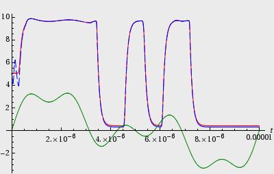
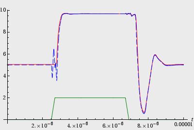
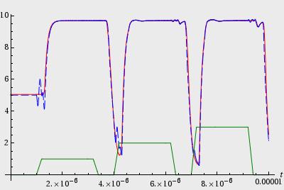
![Example Application operational amplifier op741 specification 7 subsystems symbolic reductions error bounds [%] {1,2,5,10,20,30,,90,100} 10% error](/docs-images/74/69866637/images/49-1.jpg "(entire system) transient analysis 2 distinct error functions input: sine wave excitation, 0.8 V amplitude, 1 khz frequency, T=[0 s, 0.")
49 Example Application operational amplifier op741 specification 7 subsystems symbolic reductions error bounds [%] {1,2,5,10,20,30,,90,100} 10% error (entire system) transient analysis 2 distinct error functions input: sine wave excitation, 0.8 V amplitude, 1 khz frequency, T=[0 s, s] Slide 49
50 Subsystem Ranking L²-norm 2 error functions L²-norm interval -error function similar degree of reduction different number of steps interval Slide 50
51 Reduction by Using Additional Information additional information: number of equations / terms of subsystems same specifications as before eqns. 8 7 slightly increased degree of reduction terms terms error CM PP error eqns error error Slide 51
52 Results comparison non-hierarchical, hierarchical and hybrid approach: significant savings in time models with similar quality w.r.t. number of equations and terms time cost for simulations error Slide 52


53 Results further excitations pulse sum of three sine waves sine wave Slide 53
54 Thank you for your attention. Slide 54
Coupled symbolic-numerical model reduction using the hierarchical structure of nonlinear electrical circuits
 Coupled symbolic-numerical model reduction using the hierarchical structure of nonlinear electrical circuits Model Reduction for Complex Dynamical Systems (ModRed ( 2010) TU Berlin, Berlin, Germany, December
PV-PPV: Parameter Variability Aware, Automatically Extracted, Nonlinear Time-Shifted Oscillator Macromodels
 PV-PPV: Parameter Variability Aware, Automatically Extracted, Nonlinear Time-Shifted Oscillator Macromodels Zhichun Wang, Xiaolue Lai and Jaijeet Roychowdhury Dept of ECE, University of Minnesota, Twin
Appendix. RF Transient Simulator. Page 1
 Appendix RF Transient Simulator Page 1 RF Transient/Convolution Simulation This simulator can be used to solve problems associated with circuit simulation, when the signal and waveforms involved are modulated
INF4420 Switched capacitor circuits Outline
 INF4420 Switched capacitor circuits Spring 2012 1 / 54 Outline Switched capacitor introduction MOSFET as an analog switch z-transform Switched capacitor integrators 2 / 54 Introduction Discrete time analog
! Review: MOS IV Curves and Switch Model. ! MOS Device Layout. ! Inverter Layout. ! Gate Layout and Stick Diagrams. ! Design Rules. !
 ESE 570: Digital Integrated Circuits and VLSI Fundamentals Lec 3: January 21, 2017 MOS Fabrication pt. 2: Design Rules and Layout Lecture Outline! Review: MOS IV Curves and Switch Model! MOS Device Layout!
Design and Implementation of Current-Mode Multiplier/Divider Circuits in Analog Processing
 Design and Implementation of Current-Mode Multiplier/Divider Circuits in Analog Processing N.Rajini MTech Student A.Akhila Assistant Professor Nihar HoD Abstract This project presents two original implementations
IEEE PEDS 2017, Honolulu, USA December 2017 Design of High-Voltage and High-Speed Driver
 IEEE PEDS 217, Honolulu, USA 12 15 December 217 Design of High-Voltage and High-Speed Driver Wen Li, Masami Makuuchi, and Norio Chujo Center for Technology Innovation-Production Engineering, Hitachi, Ltd.,
An Analog Phase-Locked Loop
 1 An Analog Phase-Locked Loop Greg Flewelling ABSTRACT This report discusses the design, simulation, and layout of an Analog Phase-Locked Loop (APLL). The circuit consists of five major parts: A differential
Methods and Approaches for RF Circuit Simulation And Electromagnetic Modelling
 Methods and Approaches for RF Circuit Simulation And Electromagnetic Modelling T.A.M. Kevenaar 1, E.J.W. ter Maten 1, H.H.J. Janssen 1, S. Onneweer 2 1 Philips Research, Eindhoven, The Netherlands 2 Philips
INF4420. Switched capacitor circuits. Spring Jørgen Andreas Michaelsen
 INF4420 Switched capacitor circuits Spring 2012 Jørgen Andreas Michaelsen (jorgenam@ifi.uio.no) Outline Switched capacitor introduction MOSFET as an analog switch z-transform Switched capacitor integrators
Tuesday, March 29th, 9:15 11:30
 Oscillators, Phase Locked Loops Tuesday, March 29th, 9:15 11:30 Snorre Aunet (sa@ifi.uio.no) Nanoelectronics group Department of Informatics University of Oslo Last time and today, Tuesday 29th of March:
! Review: MOS IV Curves and Switch Model. ! MOS Device Layout. ! Inverter Layout. ! Gate Layout and Stick Diagrams. ! Design Rules. !
 ESE 570: Digital Integrated Circuits and VLSI Fundamentals Lec 3: January 21, 2016 MOS Fabrication pt. 2: Design Rules and Layout Lecture Outline! Review: MOS IV Curves and Switch Model! MOS Device Layout!
ESE 570: Digital Integrated Circuits and VLSI Fundamentals
 ESE 570: Digital Integrated Circuits and VLSI Fundamentals Lec 3: January 21, 2016 MOS Fabrication pt. 2: Design Rules and Layout Penn ESE 570 Spring 2016 Khanna Adapted from GATech ESE3060 Slides Lecture
CHAPTER 1 INTRODUCTION
 CHAPTER 1 INTRODUCTION 1.1 Historical Background Recent advances in Very Large Scale Integration (VLSI) technologies have made possible the realization of complete systems on a single chip. Since complete
PROCESS-VOLTAGE-TEMPERATURE (PVT) VARIATIONS AND STATIC TIMING ANALYSIS
 VARIATIONS AND STATIC TIMING ANALYSIS") PROCESS-VOLTAGE-TEMPERATURE (PVT) VARIATIONS AND STATIC TIMING ANALYSIS The major design challenges of ASIC design consist of microscopic issues and macroscopic issues [1]. The microscopic issues are ultra-high
PROCESS-VOLTAGE-TEMPERATURE (PVT) VARIATIONS AND STATIC TIMING ANALYSIS The major design challenges of ASIC design consist of microscopic issues and macroscopic issues [1]. The microscopic issues are ultra-high
A Matlab / Simulink Based Tool for Power Electronic Circuits
 A Matlab / Simulink Based Tool for Power Electronic Circuits Abdulatif A M Shaban International Science Index, Electrical and Computer Engineering wasetorg/publication/2520 Abstract Transient simulation
Interface Electronic Circuits
 Lecture (5) Interface Electronic Circuits Part: 1 Prof. Kasim M. Al-Aubidy Philadelphia University-Jordan AMSS-MSc Prof. Kasim Al-Aubidy 1 Interface Circuits: An interface circuit is a signal conditioning
CHAPTER 4 4-PHASE INTERLEAVED BOOST CONVERTER FOR RIPPLE REDUCTION IN THE HPS
 71 CHAPTER 4 4-PHASE INTERLEAVED BOOST CONVERTER FOR RIPPLE REDUCTION IN THE HPS 4.1 INTROUCTION The power level of a power electronic converter is limited due to several factors. An increase in current
WHITE PAPER CIRCUIT LEVEL AGING SIMULATIONS PREDICT THE LONG-TERM BEHAVIOR OF ICS
 WHITE PAPER CIRCUIT LEVEL AGING SIMULATIONS PREDICT THE LONG-TERM BEHAVIOR OF ICS HOW TO MINIMIZE DESIGN MARGINS WITH ACCURATE ADVANCED TRANSISTOR DEGRADATION MODELS Reliability is a major criterion for
EE301 Electronics I , Fall
 EE301 Electronics I 2018-2019, Fall 1. Introduction to Microelectronics (1 Week/3 Hrs.) Introduction, Historical Background, Basic Consepts 2. Rewiev of Semiconductors (1 Week/3 Hrs.) Semiconductor materials
A SIGNAL DRIVEN LARGE MOS-CAPACITOR CIRCUIT SIMULATOR
 A SIGNAL DRIVEN LARGE MOS-CAPACITOR CIRCUIT SIMULATOR Janusz A. Starzyk and Ying-Wei Jan Electrical Engineering and Computer Science, Ohio University, Athens Ohio, 45701 A designated contact person Prof.
Advanced Digital Design
 Advanced Digital Design Introduction & Motivation by A. Steininger and M. Delvai Vienna University of Technology Outline Challenges in Digital Design The Role of Time in the Design The Fundamental Design
ESE 570: Digital Integrated Circuits and VLSI Fundamentals
 ESE 570: Digital Integrated Circuits and VLSI Fundamentals Lec 3: January 24, 2019 MOS Fabrication pt. 2: Design Rules and Layout Penn ESE 570 Spring 2019 Khanna Jack Keil Wolf Lecture http://www.ese.upenn.edu/about-ese/events/wolf.php
The Evolution of Waveform Relaxation for Circuit and Electromagnetic Solvers
 The Evolution of Waveform Relaxation for Circuit and Electromagnetic Solvers Albert Ruehli, Missouri S&T EMC Laboratory, University of Science & Technology, Rolla, MO with contributions by Giulio Antonini,
Introduction (concepts and definitions)
") Objectives: Introduction (digital system design concepts and definitions). Advantages and drawbacks of digital techniques compared with analog. Digital Abstraction. Synchronous and Asynchronous Systems.
Objectives: Introduction (digital system design concepts and definitions). Advantages and drawbacks of digital techniques compared with analog. Digital Abstraction. Synchronous and Asynchronous Systems.
PROJECT PERIODIC REPORT
 PROJECT PERIODIC REPORT Publishable Summary Grant Agreement number: 214911 Project acronym: Project title: Funding Scheme: ICESTARS Integrated Circuit/EM Simulation and design Technologies for Advanced
Mixed Signal Virtual Components COLINE, a case study
 Mixed Signal Virtual Components COLINE, a case study J.F. POLLET - DOLPHIN INTEGRATION Meylan - FRANCE http://www.dolphin.fr Overview of the presentation Introduction COLINE, an example of Mixed Signal
Examining a New In-Amp Architecture for Communication Satellites
 Examining a New In-Amp Architecture for Communication Satellites Introduction With more than 500 conventional sensors monitoring the condition and performance of various subsystems on a medium sized spacecraft,
ECE520 VLSI Design. Lecture 2: Basic MOS Physics. Payman Zarkesh-Ha
 ECE520 VLSI Design Lecture 2: Basic MOS Physics Payman Zarkesh-Ha Office: ECE Bldg. 230B Office hours: Wednesday 2:00-3:00PM or by appointment E-mail: pzarkesh@unm.edu Slide: 1 Review of Last Lecture Semiconductor
EINDHOVEN UNIVERSITY OF TECHNOLOGY Department of Mathematics and Computer Science. CASA-Report July 2010
 EINDHOVEN UNIVERSITY OF TECHNOLOGY Department of Mathematics and Computer Science CASA-Report 10-41 July 2010 Predicting 'parasitic effects' in large-scale circuits by E.J.W. ter Maten, J. Rommes Centre
Tuesday, March 22nd, 9:15 11:00
 Nonlinearity it and mismatch Tuesday, March 22nd, 9:15 11:00 Snorre Aunet (sa@ifi.uio.no) Nanoelectronics group Department of Informatics University of Oslo Last time and today, Tuesday 22nd of March:
Electronic-Photonic ICs for Low Cost and Scalable Datacenter Solutions
 Electronic-Photonic ICs for Low Cost and Scalable Datacenter Solutions Christoph Theiss, Director Packaging Christoph.Theiss@sicoya.com 1 SEMICON Europe 2016, October 27 2016 Sicoya Overview Spin-off from
Fundamentals of RF Design RF Back to Basics 2015
 Fundamentals of RF Design 2015 Updated January 1, 2015 Keysight EEsof EDA Objectives Review Simulation Types Understand fundamentals on S-Parameter Simulation Additional Linear and Non-Linear Simulators
CMOS VLSI IC Design. A decent understanding of all tasks required to design and fabricate a chip takes years of experience
 CMOS VLSI IC Design A decent understanding of all tasks required to design and fabricate a chip takes years of experience 1 Commonly used keywords INTEGRATED CIRCUIT (IC) many transistors on one chip VERY
CHAPTER 7 HARDWARE IMPLEMENTATION
 168 CHAPTER 7 HARDWARE IMPLEMENTATION 7.1 OVERVIEW In the previous chapters discussed about the design and simulation of Discrete controller for ZVS Buck, Interleaved Boost, Buck-Boost, Double Frequency
DAV Institute of Engineering & Technology Department of ECE. Course Outcomes
 DAV Institute of Engineering & Technology Department of ECE Course Outcomes Upon successful completion of this course, the student will intend to apply the various outcome as:: BTEC-301, Analog Devices
Computer Controlled Curve Tracer
 Computer Controlled Curve Tracer Christopher Curro The Cooper Union New York, NY Email: chris@curro.cc David Katz The Cooper Union New York, NY Email: katz3@cooper.edu Abstract A computer controlled curve
VLSI Designed Low Power Based DPDT Switch
 International Journal of Electronics and Communication Engineering. ISSN 0974-2166 Volume 8, Number 1 (2015), pp. 81-86 International Research Publication House http://www.irphouse.com VLSI Designed Low
Jack Keil Wolf Lecture. ESE 570: Digital Integrated Circuits and VLSI Fundamentals. Lecture Outline. MOSFET N-Type, P-Type.
 ESE 570: Digital Integrated Circuits and VLSI Fundamentals Jack Keil Wolf Lecture Lec 3: January 24, 2019 MOS Fabrication pt. 2: Design Rules and Layout http://www.ese.upenn.edu/about-ese/events/wolf.php
Modeling the Effect of Wire Resistance in Deep Submicron Coupled Interconnects for Accurate Crosstalk Based Net Sorting
 Modeling the Effect of Wire Resistance in Deep Submicron Coupled Interconnects for Accurate Crosstalk Based Net Sorting C. Guardiani, C. Forzan, B. Franzini, D. Pandini Adanced Research, Central R&D, DAIS,
Chapter 13: Introduction to Switched- Capacitor Circuits
 Chapter 13: Introduction to Switched- Capacitor Circuits 13.1 General Considerations 13.2 Sampling Switches 13.3 Switched-Capacitor Amplifiers 13.4 Switched-Capacitor Integrator 13.5 Switched-Capacitor
Digital Integrated Circuits A Design Perspective. The Devices. Digital Integrated Circuits 2nd Devices
 Digital Integrated Circuits A Design Perspective The Devices The Diode The diodes are rarely explicitly used in modern integrated circuits However, a MOS transistor contains at least two reverse biased
Chapter 3 Novel Digital-to-Analog Converter with Gamma Correction for On-Panel Data Driver
 Chapter 3 Novel Digital-to-Analog Converter with Gamma Correction for On-Panel Data Driver 3.1 INTRODUCTION As last chapter description, we know that there is a nonlinearity relationship between luminance
On Chip Active Decoupling Capacitors for Supply Noise Reduction for Power Gating and Dynamic Dual Vdd Circuits in Digital VLSI
 ELEN 689 606 Techniques for Layout Synthesis and Simulation in EDA Project Report On Chip Active Decoupling Capacitors for Supply Noise Reduction for Power Gating and Dynamic Dual Vdd Circuits in Digital
P a g e 1. Introduction
 P a g e 1 Introduction 1. Signals in digital form are more convenient than analog form for processing and control operation. 2. Real world signals originated from temperature, pressure, flow rate, force
Improving Test Coverage and Eliminating Test Escapes Using Analog Defect Analysis
 Improving Test Coverage and Eliminating Test Escapes Using Analog Defect Analysis Art Schaldenbrand, Dr. Walter Hartong, Amit Bajaj, Hany Elhak, and Vladimir Zivkovic, Cadence While the analog and mixed-signal
Hot Topics and Cool Ideas in Scaled CMOS Analog Design
 Engineering Insights 2006 Hot Topics and Cool Ideas in Scaled CMOS Analog Design C. Patrick Yue ECE, UCSB October 27, 2006 Slide 1 Our Research Focus High-speed analog and RF circuits Device modeling,
Assoc. Prof. Dr. Burak Kelleci
 DEPARTMENT OF ELECTRICAL &ELECTRONICS ENGINEERING ANALOG-TO-DIGITAL AND DIGITAL- TO-ANALOG CONVERTERS Assoc. Prof. Dr. Burak Kelleci Fall 2018 OUTLINE Nyquist-Rate DAC Thermometer-Code Converter Hybrid
Yet, many signal processing systems require both digital and analog circuits. To enable
 Introduction Field-Programmable Gate Arrays (FPGAs) have been a superb solution for rapid and reliable prototyping of digital logic systems at low cost for more than twenty years. Yet, many signal processing
EE 230 Lab Lab 9. Prior to Lab
 MOS transistor characteristics This week we look at some MOS transistor characteristics and circuits. Most of the measurements will be done with our usual lab equipment, but we will also use the parameter
1.3 Mixed-Signal Systems: The 555 Timer
 1.3 MIXED-SIGNAL SYSTEMS: THE 555 TIME 7 1.3 Mixed-Signal Systems: The 555 Timer Analog or digital? The 555 Timer has been around since the early 1970s. And even with the occasional new arrival of challengers
Design of a Wide Input Range DC-DC Converter Suitable for Lead-Acid Battery Charging
 ENGINEER - Vol. XXXXIV, No. 04, pp, [47-53], 2011 The Institution of Engineers, Sri Lanka Design of a Wide Input Range DC-DC Converter Suitable for Lead-Acid Battery Charging M.W.D.R. Nayanasiri and J.A.K.S.Jayasinghe,
UNIT-III POWER ESTIMATION AND ANALYSIS
 UNIT-III POWER ESTIMATION AND ANALYSIS In VLSI design implementation simulation software operating at various levels of design abstraction. In general simulation at a lower-level design abstraction offers
Chapter 4: Differential Amplifiers
 Chapter 4: Differential Amplifiers 4.1 Single-Ended and Differential Operation 4.2 Basic Differential Pair 4.3 Common-Mode Response 4.4 Differential Pair with MOS Loads 4.5 Gilbert Cell Single-Ended and
Evaluation of Package Properties for RF BJTs
 Application Note Evaluation of Package Properties for RF BJTs Overview EDA simulation software streamlines the development of digital and analog circuits from definition of concept and estimation of required
ETIN25 Analogue IC Design. Laboratory Manual Lab 2
 Department of Electrical and Information Technology LTH ETIN25 Analogue IC Design Laboratory Manual Lab 2 Jonas Lindstrand Martin Liliebladh Markus Törmänen September 2011 Laboratory 2: Design and Simulation
Capacitive Touch Sensing Tone Generator. Corey Cleveland and Eric Ponce
 Capacitive Touch Sensing Tone Generator Corey Cleveland and Eric Ponce Table of Contents Introduction Capacitive Sensing Overview Reference Oscillator Capacitive Grid Phase Detector Signal Transformer
55:041 Electronic Circuits The University of Iowa Fall Exam 3. Question 1 Unless stated otherwise, each question below is 1 point.
 Exam 3 Name: Score /65 Question 1 Unless stated otherwise, each question below is 1 point. 1. An engineer designs a class-ab amplifier to deliver 2 W (sinusoidal) signal power to an resistive load. Ignoring
Laser attacks on integrated circuits: from CMOS to FD-SOI
 DTIS 2014 9 th International Conference on Design & Technology of Integrated Systems in Nanoscale Era Laser attacks on integrated circuits: from CMOS to FD-SOI J.-M. Dutertre 1, S. De Castro 1, A. Sarafianos
Non-linear Control. Part III. Chapter 8
 Chapter 8 237 Part III Chapter 8 Non-linear Control The control methods investigated so far have all been based on linear feedback control. Recently, non-linear control techniques related to One Cycle
LSI Design Flow Development for Advanced Technology
 LSI Design Flow Development for Advanced Technology Atsushi Tsuchiya LSIs that adopt advanced technologies, as represented by imaging LSIs, now contain 30 million or more logic gates and the scale is beginning
Design of a Folded Cascode Operational Amplifier in a 1.2 Micron Silicon-Carbide CMOS Process
 University of Arkansas, Fayetteville ScholarWorks@UARK Electrical Engineering Undergraduate Honors Theses Electrical Engineering 5-2017 Design of a Folded Cascode Operational Amplifier in a 1.2 Micron
Homework Assignment 03
 Homework Assignment 03 Question 1 (Short Takes), 2 points each unless otherwise noted. 1. Two 0.68 μf capacitors are connected in series across a 10 khz sine wave signal source. The total capacitive reactance
Homework Assignment 06
 Homework Assignment 06 Question 1 (Short Takes) One point each unless otherwise indicated. 1. Consider the current mirror below, and neglect base currents. What is? Answer: 2. In the current mirrors below,
ECE 521. Design Flow. Fall 2016 Simulation. Design Verification. Why Solve Equations on a Computer?
 Design Flow Comparison with specs Redesign Concept Implementation Design Specifications Circuit Schematic ECE 521 Layout SPICE etc. Physical definition Fall 2016 Physical verification Parasitic Extraction
Substrate Coupling in RF Analog/Mixed Signal IC Design: A Review
 Substrate Coupling in RF Analog/Mixed Signal IC Design: A Review Ashish C Vora, Graduate Student, Rochester Institute of Technology, Rochester, NY, USA. Abstract : Digital switching noise coupled into
Analytical Chemistry II
 Analytical Chemistry II L3: Signal processing (selected slides) Semiconductor devices Apart from resistors and capacitors, electronic circuits often contain nonlinear devices: transistors and diodes. The
High-level synthesis of analog sensor interface front-ends
 High-level synthesis of analog sensor interface front-ends S. Donnay,G.Gielen y,w.sansen W.Kruiskamp,D.Leenaerts,W.vanBokhoven Katholieke niversiteit Leuven Eindhoven niversity of Technology Dep. Elektrotechniek,
Wire Layer Geometry Optimization using Stochastic Wire Sampling
 Wire Layer Geometry Optimization using Stochastic Wire Sampling Raymond A. Wildman*, Joshua I. Kramer, Daniel S. Weile, and Philip Christie Department University of Delaware Introduction Is it possible
A high-speed CMOS current op amp for very low supply voltage operation
 Downloaded from orbit.dtu.dk on: Mar 31, 2018 A high-speed CMOS current op amp for very low supply voltage operation Bruun, Erik Published in: Proceedings of the IEEE International Symposium on Circuits
EE 330 Laboratory 8 Discrete Semiconductor Amplifiers
 EE 330 Laboratory 8 Discrete Semiconductor Amplifiers Fall 2018 Contents Objective:...2 Discussion:...2 Components Needed:...2 Part 1 Voltage Controlled Amplifier...2 Part 2 A Nonlinear Application...3
Importance of measuring parasitic capacitance in isolated gate drive applications. W. Frank Infineon Technologies
 Importance of measuring parasitic capacitance in isolated gate drive applications W. Frank Infineon Technologies Contents 1 Why is capacitive coupling important in high voltage (HV) applications? 2 Measurement
EMC review for Belle II (Grounding & shielding plans) PXD DEPFET system
 PXD DEPFET system") EMC review for Belle II (Grounding & shielding plans) PXD DEPFET system Outline 1. Introduction 2. Grounding strategy Implementation aspects 3. Noise emission issues Test plans 4. Noise immunity issues
EMC review for Belle II (Grounding & shielding plans) PXD DEPFET system Outline 1. Introduction 2. Grounding strategy Implementation aspects 3. Noise emission issues Test plans 4. Noise immunity issues
ELT 215 Operational Amplifiers (LECTURE) Chapter 5
 Chapter 5") CHAPTER 5 Nonlinear Signal Processing Circuits INTRODUCTION ELT 215 Operational Amplifiers (LECTURE) In this chapter, we shall present several nonlinear circuits using op-amps, which include those situations
CHAPTER 5 Nonlinear Signal Processing Circuits INTRODUCTION ELT 215 Operational Amplifiers (LECTURE) In this chapter, we shall present several nonlinear circuits using op-amps, which include those situations
High-Performance Analog and RF Circuit Simulation using the Analog FastSPICE Platform at Columbia University. Columbia University
 High-Performance Analog and RF Circuit Simulation using the Analog FastSPICE Platform at Columbia University By: K. Tripurari, C. W. Hsu, J. Kuppambatti, B. Vigraham, P.R. Kinget Columbia University For
Experiment 3 - IC Resistors
 Experiment 3 - IC Resistors.T. Yeung, Y. Shin,.Y. Leung and R.T. Howe UC Berkeley EE 105 1.0 Objective This lab introduces the Micro Linear Lab Chips, with measurements of IC resistors and a distributed
Lab 8 D/A Conversion and Waveform Generation Lab Time: 9-12pm Wednesday Lab Partner: Chih-Chieh Wang (Dennis) EE145M Station 13
 EE145M Station 13") Lab 8 D/A Conversion and Waveform Generation Bill Hung Lab Time: 9-12pm Wednesday 17508938 Lab Partner: Chih-Chieh Wang (Dennis) EE145M Station 13 Aim Interface with a digital-to-analog (D/A) converter
Lab 8 D/A Conversion and Waveform Generation Bill Hung Lab Time: 9-12pm Wednesday 17508938 Lab Partner: Chih-Chieh Wang (Dennis) EE145M Station 13 Aim Interface with a digital-to-analog (D/A) converter
Lecture 11: Clocking
 High Speed CMOS VLSI Design Lecture 11: Clocking (c) 1997 David Harris 1.0 Introduction We have seen that generating and distributing clocks with little skew is essential to high speed circuit design.
Integrated Circuit Design for High-Speed Frequency Synthesis
 Integrated Circuit Design for High-Speed Frequency Synthesis John Rogers Calvin Plett Foster Dai ARTECH H O US E BOSTON LONDON artechhouse.com Preface XI CHAPTER 1 Introduction 1 1.1 Introduction to Frequency
Examining a New In-Amp Architecture for Communication Satellites
 White Paper Examining a New In-Amp Architecture for Communication Satellites Introduction With more 500 conventional sensors monitoring the condition and performance of various subsystems on a medium sized
Intelligent Systems Group Department of Electronics. An Evolvable, Field-Programmable Full Custom Analogue Transistor Array (FPTA)
") Department of Electronics n Evolvable, Field-Programmable Full Custom nalogue Transistor rray (FPT) Outline What`s Behind nalog? Evolution Substrate custom made configurable transistor array (FPT) Ways
Department of Electronics n Evolvable, Field-Programmable Full Custom nalogue Transistor rray (FPT) Outline What`s Behind nalog? Evolution Substrate custom made configurable transistor array (FPT) Ways
I1 19u 5V R11 1MEG IDC Q7 Q2N3904 Q2N3904. Figure 3.1 A scaled down 741 op amp used in this lab
 Lab 3: 74 Op amp Purpose: The purpose of this laboratory is to become familiar with a two stage operational amplifier (op amp). Students will analyze the circuit manually and compare the results with SPICE.
Advanced Digital Design
 Advanced Digital Design The Need for a Design Style by A. Steininger Vienna University of Technology Outline Skew versus consistency The need for a design style Hazards, Glitches & Runts Lecture "Advanced
A Low-Jitter Phase-Locked Loop Based on a Charge Pump Using a Current-Bypass Technique
 JOURNAL OF SEMICONDUCTOR TECHNOLOGY AND SCIENCE, VOL.14, NO.3, JUNE, 2014 http://dx.doi.org/10.5573/jsts.2014.14.3.331 A Low-Jitter Phase-Locked Loop Based on a Charge Pump Using a Current-Bypass Technique
Scientific (super)computing in the electronics industry
computing in the electronics industry") Scientific (super)computing in the electronics industry Wil Schilders Centre for Analysis, Scientific Computing and Applications & Platform Wiskunde Nederland SARA Superdag, December 1, 2010 Centre for
Scientific (super)computing in the electronics industry Wil Schilders Centre for Analysis, Scientific Computing and Applications & Platform Wiskunde Nederland SARA Superdag, December 1, 2010 Centre for
Analogue Electronic Systems
 Unit 47: Unit code Analogue Electronic Systems F/615/1515 Unit level 5 Credit value 15 Introduction Analogue electronic systems are still widely used for a variety of very important applications and this
SCHMITT TRIGGER. Typical ``real world'' signals consist of a superposition of a ``noise'' signal and a
 SCHMITT TRIGGER Typical ``real world'' signals consist of a superposition of a ``noise'' signal and a signal or signals of interest. For example, the signal at the bottom of Figure 19 shows a superposition
Dr. Ralf Sommer. Munich, March 8th, 2006 COM BTS DAT DF AMF. Presenter Dept Titel presentation Date Page 1
 DATE 2006 Special Session: DFM/DFY Design for Manufacturability and Yield - Influence of Process Variations in Digital, Analog and Mixed-Signal Circuit Design DATE 06 Munich, March 8th, 2006 Presenter
Noise Constraint Driven Placement for Mixed Signal Designs. William Kao and Wenkung Chu October 20, 2003 CAS IEEE SCV Meeting
 Noise Constraint Driven Placement for Mixed Signal Designs William Kao and Wenkung Chu October 20, 2003 CAS IEEE SCV Meeting Introduction OUTLINE Substrate Noise: Some Background Substrate Noise Network
LM392/LM2924 Low Power Operational Amplifier/Voltage Comparator
 LM392/LM2924 Low Power Operational Amplifier/Voltage Comparator General Description The LM392 series consists of 2 independent building block circuits. One is a high gain, internally frequency compensated
New Techniques for Testing Power Factor Correction Circuits
 Keywords Venable, frequency response analyzer, impedance, injection transformer, oscillator, feedback loop, Bode Plot, power supply design, power factor correction circuits, current mode control, gain
PowerAmp Design. PowerAmp Design PAD117A RAIL TO RAIL OPERATIONAL AMPLIFIER
 PowerAmp Design RAIL TO RAIL OPERATIONAL AMPLIFIER Rev J KEY FEATURES LOW COST RAIL TO RAIL INPUT & OUTPUT SINGLE SUPPLY OPERATION HIGH VOLTAGE 100 VOLTS HIGH OUTPUT CURRENT 15A 250 WATT OUTPUT CAPABILITY
EE 330 Laboratory 8 Discrete Semiconductor Amplifiers
 EE 330 Laboratory 8 Discrete Semiconductor Amplifiers Fall 2017 Contents Objective:... 2 Discussion:... 2 Components Needed:... 2 Part 1 Voltage Controlled Amplifier... 2 Part 2 Common Source Amplifier...
INF4420. Outline. Switched capacitor circuits. Switched capacitor introduction. MOSFET as an analog switch 1 / 26 2 / 26.
 INF4420 Switched capacitor circuits Spring 2012 Jørgen Andreas Michaelsen (jorgenam@ifi.uil.no) 1 / 26 Outline Switched capacitor introduction MOSFET as an analog switch 2 / 26 Introduction Discrete time
Continuous-Time Systems
 Continuous-Time Systems Continuous time waveforms Analog RF High-freq./speed continuous time Radio design community today: analog ~= RF Bluetooth chip (Cambridge Silicon) Mixed-signal Low-freq. Continuous-time
ECE 484 VLSI Digital Circuits Fall Lecture 02: Design Metrics
 ECE 484 VLSI Digital Circuits Fall 2016 Lecture 02: Design Metrics Dr. George L. Engel Adapted from slides provided by Mary Jane Irwin (PSU) [Adapted from Rabaey s Digital Integrated Circuits, 2002, J.
ECE 415/515 ANALOG INTEGRATED CIRCUIT DESIGN
 ECE 415/515 ANALOG INTEGRATED CIRCUIT DESIGN OPAMP DESIGN AND SIMULATION Vishal Saxena OPAMP DESIGN PROJECT R 2 v out v in /2 R 1 C L v in v out V CM R L V CM C L V CM -v in /2 R 1 C L (a) (b) R 2 ECE415/EO
CMOS Digital Integrated Circuits Lec 11 Sequential CMOS Logic Circuits
 Lec Sequential CMOS Logic Circuits Sequential Logic In Combinational Logic circuit Out Memory Sequential The output is determined by Current inputs Previous inputs Output = f(in, Previous In) The regenerative
Circuit Applications of Multiplying CMOS D to A Converters
 Circuit Applications of Multiplying CMOS D to A Converters The 4-quadrant multiplying CMOS D to A converter (DAC) is among the most useful components available to the circuit designer Because CMOS DACs
ELC224 Final Review (12/10/2009) Name:
 Name:") ELC224 Final Review (12/10/2009) Name: Select the correct answer to the problems 1 through 20. 1. A common-emitter amplifier that uses direct coupling is an example of a dc amplifier. 2. The frequency
ELC224 Final Review (12/10/2009) Name: Select the correct answer to the problems 1 through 20. 1. A common-emitter amplifier that uses direct coupling is an example of a dc amplifier. 2. The frequency