University of Minnesota, Minneapolis, MN 2. Intel Corporation, Hillsboro, OR 3. Los Alamos National Laboratory, Los Alamos, NM
|
|
|
- Elwin Bridges
- 6 years ago
- Views:
Transcription
1 Statistical Characterization of Radiation- Induced Pulse Waveforms and Flip-Flop Soft Errors in 14nm Tri-Gate CMOS Using a Back- Sampling Chain (BSC) Technique Saurabh Kumar 1, M. Cho 2, L. Everson 1, H. Kim 1, Q. Tang 1, P. Mazanec 1, P. Meinerzhagen 2, A. Malavasi 2, D. Lake 2, C. Tokunaga 2, H. Quinn 3, M. Khellah 2, J. Tschanz 2, S. Borkar 2, V. De 2 and C. H. Kim 1 1 University of Minnesota, Minneapolis, MN 2 Intel Corporation, Hillsboro, OR 3 Los Alamos National Laboratory, Los Alamos, NM kumar175@umn.edu This research was, in part, funded by the U.S. government. The views and conclusions contained in this document are those of the authors and should not be interpreted as representing the official policies, either expressed or implied, of the U.S. government Symposia on VLSI Technology and Circuits
2 Outline Motivation Back-sampling chain (BSC) technique 14nm test-chip and board design Neutron irradiation test results Strike pulse re-construction results Conclusion Slide 1
 S.")
3 S Soft Error: Planar vs. Tri-Gate D G G Fin S D Charge collection Charge collection Device level soft error rate has been decreasing with scaling FIT/Mb (Log Scale) S. Lee et. al. IRPS 2015 Planar Finfet High energy neutron Alpha particle Thermal neutron Technology (nm) Slide 2
4 Scaling Impact on SER in Tri-Gate G Smaller crosssection S D Narrower path 14nm 10nm Lower SER with tri-gate scaling Taller/narrower fins, higher resistance Smaller cross-section Slide 3
5 Scaling Impact on SER in Tri-Gate Transistor density (MTr / mm 2 ) nm 32nm 22nm 14nm Year of production 10nm Supply Voltage (a.u.) Lower per-transistor SER Higher transistor count, lower VDD increased chip-level SER Challenge: Collecting statistically significant amount of data in limited beam time Slide 4
6 Logic SET vs. Sequential SEU/MBU 1 1 D Clk 1 0 Clk To slave Clk Clk Clk Combinational logic path Flop storage node VDD VDD Vnode Trip point of next stage Vnode Flipping threshold Time Time Slide 5
7 Circuit Dependencies 1 V node I strike P 1 P 2 1 For higher SER sensitivity: - I restore - I strike - C node - V sw N 1 V sw N 2 I restore C node : High V T, smaller size (N 1 ) : High flux/let (radiation parameter) : Small fan-out, device size : High V T, smaller device (P 2 ) Slide 6
8 Technique #1: Current Starved Buffers Long chain of current starved buffers: detection circuit Starved buffer chain: High sensitivity Slide 7
9 Technique #1: Current Starved Buffers SER strike V PO V PE V PO V PE V NO V NE V NO V NE Alternate starving: Lower I restore, lower V sw Analog bias knobs: Tunable resolution and sensitivity Critical charge (Qcrit, normalized) Standard chain This work 1x INV, TT, 27 C Higher sensitivity Voltage (V) Slide 8
10 Technique #2: Back-Sampling Chain SER strike V PO V PE V PO V PE V NO V NE V NO V NE N2 Later stage rising edge back-samples previous stage falling edge Stage Output # of 0's indicate original pulse width Time Slide 9
11 Example: Short vs. Long Strike Pulse Stage Output Unsampled original bits Long trail of 0's Stage Output Unsampled original bits Short trail of 0's Time Time Slide 10
12 Min. detection amplitude (normalized to VDD) Tunable Resolution and Sensitivity Sensitivity vs resolution trade-off Resolution (ps) Allows multiple resolution-sensitivity sweeps Facilitates strike pulse re-construction V PO V NO V PE V PO V PE V NE V NO V NE N2 Slide 11


13 Back-Sampling Chain (BSC) Array Buff In Scan Out Q D Q D Q D D Q D Q D Q Q D Q D Q D D Q D Q D Q Unit Cell C1 Q D Q D Q D Scan In D Q D Q D Q Buff Out Q D Q D Q D D Q D Q D Q Slide 12


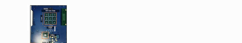
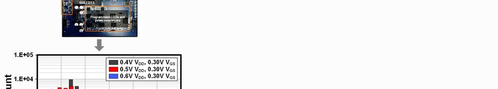
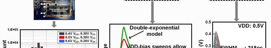
14 SER Test Board Fabricated Board Beam diameter = 3 inches 3x3 SER test-chips fit within beam area FPGA: JTAG support for automated control 15.3 million BSC stages per board Slide 13


15 LANL Neutron Irradiation Test 10 stacked boards with 90 test-chips in parallel irradiated under neutron beam at Los Alamos National Laboratory (LANL) Slide 14


16 Neutron Beam Parameters Source: Los Alamos National Laboratory Neutron beam specs Avg. energy spectrum range: MeV Avg. neutron flux: ~ 4.2x10 4 neutrons/cm 2 /s Slide 15
17 Neutron Test Data: SET A strike on buffer node induces SET FF Data = FF Data = Slide 16

18 Neutron Test Data: SEU/ MBU A strike on flop storage node induces SEU/ MBU FF Data = SEU FF Data = MBU Slide 17
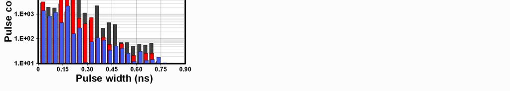
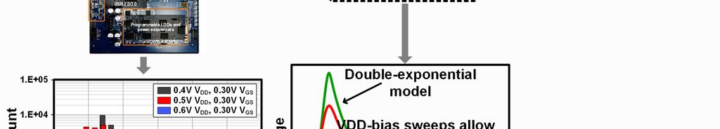
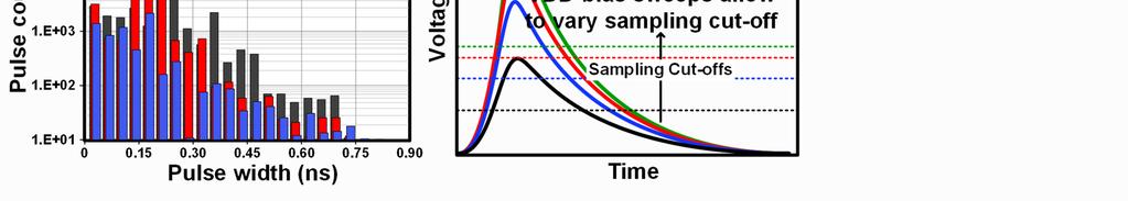
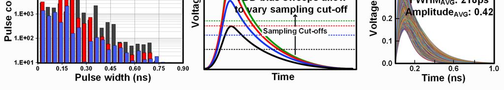
19 Strike Pulse Width Distribution 1.E+05 Pulse count 1.E+04 1.E+03 1.E+02 Voltage Time 0.40V V DD, 0.30V V GS 0.50V V DD, 0.30V V GS 0.60V V DD, 0.30V V GS 0.6V Sampling 0.5V 0.4V cut-offs 1.E Pulse width (ns) With lower VDD, sampling cut-off drops and wider SET pulses are sampled Q crit decreases with lower VDD, increasing SER Slide 18
20 Strike Pulse Width Distribution 1.E+05 Pulse count 1.E+04 1.E+03 1.E+02 Voltage 0.40V V DD, 0.20V V GS 0.40V V DD, 0.25V V GS 0.40V V DD, 0.30V V GS Time 0.30V V GS 0.25V V GS Sampling 0.20V V GS cut-offs 1.E Pulse width (ns) With stronger starving (lower V GS ), sensitivity increases and sampling threshold drops, sampling wider SET pulses Slide 19
21 SET Pulse Re-construction Slide 20

22 SET Pulse Re-construction Slide 21
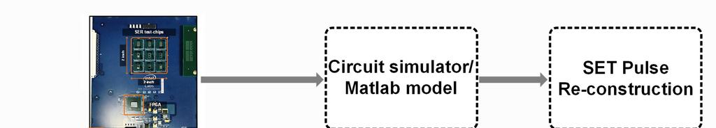
23 SET Pulse Re-construction FWHM: Full width at half maximum Slide 22


24 SET Pulse Re-construction FWHM: Full width at half maximum Higher amplitude = shorter pulse width (lower FWHM) To our knowledge, this is the first time individual strike pulses are reconstructed Slide 23
25 SET Pulse Re-construction 0.5 VDD=0.5V VDD=0.4V Voltage (V) FWHM AVG : 218ps Amplitude AVG : 0.42 FWHM AVG : 222 ps Amplitude AVG : Time (ns) Time (ns) Lower VDD: pulse amplitude, pulse width Slide 24
26 Comparison with Prior Art To TDC TDC based circuit [1] Pulse shrinking [2] This work Unit cell layout Irregular, not easily scalable Regular, scalable Regular, scalable Sensitivity tuning Fixed by design Fixed by design Variable using bias knobs * Resolution > 30ps > 1ps > 1.3ps Q crit sensitivity * 1x 0.6x 9x * Results reproduced in 14nm process [1] T. D. Loveless et. al. TNS 2012 [2] J. Furuta et.al. IRPS 2011 Slide 25
27 Flip-Flop SEU/MBU Failure In Time (normalized) FIT: # of SER per flop per billion hours Cross-section (normalized) bit 4-bit 3-bit bit 1-bit VDD (V) VDD (V) SER exponentially increases with lower VDD At lower VDDs, MBU become more dominant Slide 26
28 Conclusion BSC chain technique proposed with 9x lower Q crit and picosecond range resolution BSC circuit detects SET, SEU, and MBU 14nm test-chip irradiated under neutron beam Individual strike pulses re-constructed based on neutron irradiation data Next step: SER model framework development Slide 27
RTN Induced Frequency Shift Measurements Using a Ring Oscillator Based Circuit
 RTN Induced Frequency Shift Measurements Using a Ring Oscillator Based Circuit Qianying Tang 1, Xiaofei Wang 1, John Keane 2, and Chris H. Kim 1 1 University of Minnesota, Minneapolis, MN 2 Intel Corporation,
A 10Gb/s 10mm On-Chip Serial Link in 65nm CMOS Featuring a Half-Rate Time-Based Decision Feedback Equalizer
 A 10Gb/s 10mm On-Chip Serial Link in 65nm CMOS Featuring a Half-Rate Time-Based Decision Feedback Equalizer Po-Wei Chiu, Somnath Kundu, Qianying Tang, and Chris H. Kim University of Minnesota, Minneapolis,
The Effect of Threshold Voltages on the Soft Error Rate. - V Degalahal, N Rajaram, N Vijaykrishnan, Y Xie, MJ Irwin
 The Effect of Threshold Voltages on the Soft Error Rate - V Degalahal, N Rajaram, N Vijaykrishnan, Y Xie, MJ Irwin Outline Introduction Soft Errors High Threshold ( V t ) Charge Creation Logic Attenuation
Method for Qcrit Measurement in Bulk CMOS Using a Switched Capacitor Circuit
 Method for Qcrit Measurement in Bulk CMOS Using a Switched Capacitor Circuit John Keane Alan Drake AJ KleinOsowski Ethan H. Cannon * Fadi Gebara Chris Kim jkeane@ece.umn.edu adrake@us.ibm.com ajko@us.ibm.com
Single Event Transient Effects on Microsemi ProASIC Flash-based FPGAs: analysis and possible solutions
 Single Event Transient Effects on Microsemi ProASIC Flash-based FPGAs: analysis and possible solutions L. Sterpone Dipartimento di Automatica e Informatica Politecnico di Torino, Torino, ITALY 1 Motivations
Design of Soft Error Tolerant Memory and Logic Circuits
 Design of Soft Error Tolerant Memory and Logic Circuits Shah M. Jahinuzzaman PhD Student http://vlsi.uwaterloo.ca/~smjahinu Graduate Student Research Talks, E&CE January 16, 2006 CMOS Design and Reliability
Dependence of Cell Distance and Well-Contact Density on MCU Rates by Device Simulations and Neutron Experiments in a 65-nm Bulk Process
 IEEE TRANSACTIONS ON NUCLEAR SCIENCE, VOL. 61, NO. 4, AUGUST 2014 1583 Dependence of Cell Distance and Well-Contact Density on MCU Rates by Device Simulations and Neutron Experiments in a 65-nm Bulk Process
Duty-Cycle Shift under Asymmetric BTI Aging: A Simple Characterization Method and its Application to SRAM Timing
 Duty-Cycle Shift under Asymmetric BTI Aging: A Simple Characterization Method and its Application to SRAM Timing 1 Xiaofei Wang, 2 John Keane, 2 Pulkit Jain, 3 Vijay Reddy and 1 Chris H. Kim 1 University
Digital Integrated Circuits Designing Combinational Logic Circuits. Fuyuzhuo
 Digital Integrated Circuits Designing Combinational Logic Circuits Fuyuzhuo Introduction Digital IC Combinational vs. Sequential Logic In Combinational Logic Circuit Out In Combinational Logic Circuit
2009 Spring CS211 Digital Systems & Lab 1 CHAPTER 3: TECHNOLOGY (PART 2)
") 1 CHAPTER 3: IMPLEMENTATION TECHNOLOGY (PART 2) Whatwillwelearninthischapter? we learn in this 2 How transistors operate and form simple switches CMOS logic gates IC technology FPGAs and other PLDs Basic
1 CHAPTER 3: IMPLEMENTATION TECHNOLOGY (PART 2) Whatwillwelearninthischapter? we learn in this 2 How transistors operate and form simple switches CMOS logic gates IC technology FPGAs and other PLDs Basic
Digital Integrated Circuits Designing Combinational Logic Circuits. Fuyuzhuo
 Digital Integrated Circuits Designing Combinational Logic Circuits Fuyuzhuo Introduction Digital IC Combinational vs. Sequential Logic In Combinational Logic Circuit Out In Combinational Logic Circuit
Interconnect-Power Dissipation in a Microprocessor
 4/2/2004 Interconnect-Power Dissipation in a Microprocessor N. Magen, A. Kolodny, U. Weiser, N. Shamir Intel corporation Technion - Israel Institute of Technology 4/2/2004 2 Interconnect-Power Definition
CHAPTER 7 A BICS DESIGN TO DETECT SOFT ERROR IN CMOS SRAM
 131 CHAPTER 7 A BICS DESIGN TO DETECT SOFT ERROR IN CMOS SRAM 7.1 INTRODUCTION Semiconductor memories are moving towards higher levels of integration. This increase in integration is achieved through reduction
IMPACT OF DESIGNER-CONTROLLED PARAMETERS ON SINGLE-EVENT RESPONSES FOR FLIP-FLOP DESIGNS IN ADVANCED TECHNOLOGIES. Hangfang Zhang.
 IMPACT OF DESIGNER-CONTROLLED PARAMETERS ON SINGLE-EVENT RESPONSES FOR FLIP-FLOP DESIGNS IN ADVANCED TECHNOLOGIES By Hangfang Zhang Dissertation Submitted to the Faculty of the Graduate School of Vanderbilt
A New Low Power High Reliability Flip-Flop Robust Against Process Variations
 http://jecei.srttu.edu Journal of Electrical and Computer Engineering Innovations SRTTU JECEI, Vol. 4, No. 2, 2016 Regular Paper A New Low Power High Reliability Flip-Flop Robust Against Process Variations
SIMMAT A Metastability Analysis Tool
 SIMMAT A Metastability Analysis Tool Simulation waveforms voltage d q Ian W. Jones and Suwen Yang, Oracle Labs, Mark Greenstreet, University of British Columbia clk time (ns) 1 November 2012 1 Outline
Modeling the Impact of Device and Pipeline Scaling on the Soft Error Rate of Processor Elements
 Modeling the Impact of Device and Pipeline Scaling on the Soft Error Rate of Processor Elements Department of Computer Sciences Technical Report 2002-19 Premkishore Shivakumar Michael Kistler Stephen W.
Fin-Shaped Field Effect Transistor (FinFET) Min Ku Kim 03/07/2018
 Min Ku Kim 03/07/2018") Fin-Shaped Field Effect Transistor (FinFET) Min Ku Kim 03/07/2018 ECE 658 Sp 2018 Semiconductor Materials and Device Characterizations OUTLINE Background FinFET Future Roadmap Keeping up w/ Moore s Law
Fin-Shaped Field Effect Transistor (FinFET) Min Ku Kim 03/07/2018 ECE 658 Sp 2018 Semiconductor Materials and Device Characterizations OUTLINE Background FinFET Future Roadmap Keeping up w/ Moore s Law
The challenges of low power design Karen Yorav
 The challenges of low power design Karen Yorav The challenges of low power design What this tutorial is NOT about: Electrical engineering CMOS technology but also not Hand waving nonsense about trends
CPE/EE 427, CPE 527 VLSI Design I: Homeworks 3 & 4
 CPE/EE 427, CPE 527 VLSI Design I: Homeworks 3 & 4 1 2 3 4 5 6 7 8 9 10 Sum 30 10 25 10 30 40 10 15 15 15 200 1. (30 points) Misc, Short questions (a) (2 points) Postponing the introduction of signals
Low Power Radiation Tolerant CMOS Design using Commercial Fabrication Processes
 Low Power Radiation Tolerant CMOS Design using Commercial Fabrication Processes Amir Hasanbegovic (amirh@ifi.uio.no) Nanoelectronics Group, Dept. of Informatics, University of Oslo November 5, 2010 Overview
Extending Modular Redundancy to NTV: Costs and Limits of Resiliency at Reduced Supply Voltage
 Extending Modular Redundancy to NTV: Costs and Limits of Resiliency at Reduced Supply Voltage Rizwan A. Ashraf, A. Al-Zahrani, and Ronald F. DeMara Department of Electrical Engineering and Computer Science
EECS 427 Lecture 22: Low and Multiple-Vdd Design
 EECS 427 Lecture 22: Low and Multiple-Vdd Design Reading: 11.7.1 EECS 427 W07 Lecture 22 1 Last Time Low power ALUs Glitch power Clock gating Bus recoding The low power design space Dynamic vs static EECS
ESE 570: Digital Integrated Circuits and VLSI Fundamentals
 ESE 570: Digital Integrated Circuits and VLSI Fundamentals Lec 3: January 24, 2019 MOS Fabrication pt. 2: Design Rules and Layout Penn ESE 570 Spring 2019 Khanna Jack Keil Wolf Lecture http://www.ese.upenn.edu/about-ese/events/wolf.php
An Array-Based Circuit for Characterizing Latent Plasma-Induced Damage
 An Array-Based Circuit for Characterizing Latent Plasma-Induced Damage Won Ho Choi, Pulkit Jain and Chris H. Kim University of Minnesota, Minneapolis, MN choi0444@umn.edu www.umn.edu/~chriskim/ Purpose
Effect of Aging on Power Integrity of Digital Integrated Circuits
 Effect of Aging on Power Integrity of Digital Integrated Circuits A. Boyer, S. Ben Dhia Alexandre.boyer@laas.fr Sonia.bendhia@laas.fr 1 May 14 th, 2013 Introduction and context Long time operation Harsh
A Novel Latch design for Low Power Applications
 A Novel Latch design for Low Power Applications Abhilasha Deptt. of Electronics and Communication Engg., FET-MITS Lakshmangarh, Rajasthan (India) K. G. Sharma Suresh Gyan Vihar University, Jagatpura, Jaipur,
Silicon Odometer: An On-Chip Reliability Monitor for Measuring Frequency Degradation of Digital Circuits
 Silicon Odometer: An On-Chip Reliability Monitor for Measuring Frequency Degradation of Digital Circuits Tae-Hyoung Kim, Randy Persaud and Chris H. Kim Department of Electrical and Computer Engineering
Semiconductor Memory: DRAM and SRAM. Department of Electrical and Computer Engineering, National University of Singapore
 Semiconductor Memory: DRAM and SRAM Outline Introduction Random Access Memory (RAM) DRAM SRAM Non-volatile memory UV EPROM EEPROM Flash memory SONOS memory QD memory Introduction Slow memories Magnetic
Leakage Power Minimization in Deep-Submicron CMOS circuits
 Outline Leakage Power Minimization in Deep-Submicron circuits Politecnico di Torino Dip. di Automatica e Informatica 1019 Torino, Italy enrico.macii@polito.it Introduction. Design for low leakage: Basics.
Jack Keil Wolf Lecture. ESE 570: Digital Integrated Circuits and VLSI Fundamentals. Lecture Outline. MOSFET N-Type, P-Type.
 ESE 570: Digital Integrated Circuits and VLSI Fundamentals Jack Keil Wolf Lecture Lec 3: January 24, 2019 MOS Fabrication pt. 2: Design Rules and Layout http://www.ese.upenn.edu/about-ese/events/wolf.php
FinFET-based Design for Robust Nanoscale SRAM
 FinFET-based Design for Robust Nanoscale SRAM Prof. Tsu-Jae King Liu Dept. of Electrical Engineering and Computer Sciences University of California at Berkeley Acknowledgements Prof. Bora Nikoli Zheng
ECE 5745 Complex Digital ASIC Design Topic 2: CMOS Devices
 ECE 5745 Complex Digital ASIC Design Topic 2: CMOS Devices Christopher Batten School of Electrical and Computer Engineering Cornell University http://www.csl.cornell.edu/courses/ece5950 Simple Transistor
CHAPTER 3 PERFORMANCE OF A TWO INPUT NAND GATE USING SUBTHRESHOLD LEAKAGE CONTROL TECHNIQUES
 CHAPTER 3 PERFORMANCE OF A TWO INPUT NAND GATE USING SUBTHRESHOLD LEAKAGE CONTROL TECHNIQUES 41 In this chapter, performance characteristics of a two input NAND gate using existing subthreshold leakage
A BUILT-IN SELF-TEST (BIST) TECHNIQUE FOR SINGLE-EVENT TRANSIENT TESTING IN DIGITAL CIRCUITS. Anitha Balasubramanian. Thesis
 TECHNIQUE FOR SINGLE-EVENT TRANSIENT TESTING IN DIGITAL CIRCUITS. Anitha Balasubramanian. Thesis") A BUILT-IN SELF-TEST (BIST) TECHNIQUE FOR SINGLE-EVENT TRANSIENT TESTING IN DIGITAL CIRCUITS By Anitha Balasubramanian Thesis Submitted to the Faculty of the Graduate School of Vanderbilt University in
A BUILT-IN SELF-TEST (BIST) TECHNIQUE FOR SINGLE-EVENT TRANSIENT TESTING IN DIGITAL CIRCUITS By Anitha Balasubramanian Thesis Submitted to the Faculty of the Graduate School of Vanderbilt University in
A 4 Channel Waveform Sampling ASIC in 130 nm CMOS
 A 4 Channel Waveform Sampling ASIC in 130 nm CMOS E. Oberla, H. Grabas, J.F. Genat, H. Frisch Enrico Fermi Institute, University of Chicago K. Nishimura, G. Varner University of Hawai I Large Area Picosecond
! Review: MOS IV Curves and Switch Model. ! MOS Device Layout. ! Inverter Layout. ! Gate Layout and Stick Diagrams. ! Design Rules. !
 ESE 570: Digital Integrated Circuits and VLSI Fundamentals Lec 3: January 21, 2017 MOS Fabrication pt. 2: Design Rules and Layout Lecture Outline! Review: MOS IV Curves and Switch Model! MOS Device Layout!
EECS150 - Digital Design Lecture 15 - CMOS Implementation Technologies. Overview of Physical Implementations
 EECS150 - Digital Design Lecture 15 - CMOS Implementation Technologies Mar 12, 2013 John Wawrzynek Spring 2013 EECS150 - Lec15-CMOS Page 1 Overview of Physical Implementations Integrated Circuits (ICs)
1 Digital EE141 Integrated Circuits 2nd Introduction
 Digital Integrated Circuits Introduction 1 What is this lecture about? Introduction to digital integrated circuits + low power circuits Issues in digital design The CMOS inverter Combinational logic structures
EECS150 - Digital Design Lecture 9 - CMOS Implementation Technologies
 EECS150 - Digital Design Lecture 9 - CMOS Implementation Technologies Feb 14, 2012 John Wawrzynek Spring 2012 EECS150 - Lec09-CMOS Page 1 Overview of Physical Implementations Integrated Circuits (ICs)
Advanced Digital Integrated Circuits. Lecture 2: Scaling Trends. Announcements. No office hour next Monday. Extra office hour Tuesday 2-3pm
 EE241 - Spring 20 Advanced Digital Integrated Circuits Lecture 2: Scaling Trends and Features of Modern Technologies Announcements No office hour next Monday Extra office hour Tuesday 2-3pm 2 1 Outline
Development of a 20 GS/s Sampling Chip in 130nm CMOS Technology
 Development of a 20 GS/s Sampling Chip in 130nm CMOS Technology 2009 IEEE Nuclear Science Symposium, Orlando, Florida, October 28 th 2009 Jean-Francois Genat On behalf of Mircea Bogdan 1, Henry J. Frisch
Towards PVT-Tolerant Glitch-Free Operation in FPGAs
 Towards PVT-Tolerant Glitch-Free Operation in FPGAs Safeen Huda and Jason H. Anderson ECE Department, University of Toronto, Canada 24 th ACM/SIGDA International Symposium on FPGAs February 22, 2016 Motivation
CMOS Transistor and Circuits. Jan 2015 CMOS Transistor 1
 CMOS Transistor and Circuits Jan 2015 CMOS Transistor 1 Latchup in CMOS Circuits Jan 2015 CMOS Transistor 2 Parasitic bipolar transistors are formed by substrate and source / drain devices Latchup occurs
CHAPTER 6 DESIGN OF VOLTAGE CONTROLLED OSCILLATOR (VCO) USING 45 NM VLSI TECHNOLOGY
 USING 45 NM VLSI TECHNOLOGY") CHAPTER 6 DESIGN OF VOLTAGE CONTROLLED OSCILLATOR (VCO) USING 45 NM VLSI TECHNOLOGY Oscillators are required to generate the carrying signals for radio frequency transmission, but also for the main clocks
CHAPTER 6 DESIGN OF VOLTAGE CONTROLLED OSCILLATOR (VCO) USING 45 NM VLSI TECHNOLOGY Oscillators are required to generate the carrying signals for radio frequency transmission, but also for the main clocks
Lecture 9: Clocking for High Performance Processors
 Lecture 9: Clocking for High Performance Processors Computer Systems Lab Stanford University horowitz@stanford.edu Copyright 2001 Mark Horowitz EE371 Lecture 9-1 Horowitz Overview Reading Bailey Stojanovic
Fast Characterization of PBTI and NBTI Induced Frequency Shifts under a Realistic Recovery Bias Using a Ring Oscillator Based Circuit
 Fast Characterization of PBTI and NBTI Induced Frequency Shifts under a Realistic Recovery Bias Using a Ring Oscillator Based Circuit 1,2 Xiaofei Wang, 1 Seung-hwan Song, 1 Ayan Paul and 1 Chris H. Kim
A New Asymmetric SRAM Cell to Reduce Soft Errors and Leakage Power in FPGA
 A New Asymmetric SRAM Cell to Reduce Soft Errors and Leakage Power in FPGA Balkaran S. Gill, Chris Papachristou, and Francis G. Wolff Department of Electrical Engineering and Computer Science Case Western
EECS 141: SPRING 98 FINAL
 University of California College of Engineering Department of Electrical Engineering and Computer Science J. M. Rabaey 511 Cory Hall TuTh3:3-5pm e141@eecs EECS 141: SPRING 98 FINAL For all problems, you
A 4-Channel Fast Waveform Sampling ASIC in 130 nm CMOS
 A 4-Channel Fast Waveform Sampling ASIC in 130 nm CMOS E. Oberla, H. Grabas, M. Bogdan, J.F. Genat, H. Frisch Enrico Fermi Institute, University of Chicago K. Nishimura, G. Varner University of Hawai I
EECS150 - Digital Design Lecture 19 CMOS Implementation Technologies. Recap and Outline
 EECS150 - Digital Design Lecture 19 CMOS Implementation Technologies Oct. 31, 2013 Prof. Ronald Fearing Electrical Engineering and Computer Sciences University of California, Berkeley (slides courtesy
Electronic Circuits EE359A
 Electronic Circuits EE359A Bruce McNair B206 bmcnair@stevens.edu 201-216-5549 1 Memory and Advanced Digital Circuits - 2 Chapter 11 2 Figure 11.1 (a) Basic latch. (b) The latch with the feedback loop opened.
EE 434 ASIC and Digital Systems. Prof. Dae Hyun Kim School of Electrical Engineering and Computer Science Washington State University.
 EE 434 ASIC and Digital Systems Prof. Dae Hyun Kim School of Electrical Engineering and Computer Science Washington State University Preliminaries VLSI Design System Specification Functional Design RTL
Optimization of power in different circuits using MTCMOS Technique
 Optimization of power in different circuits using MTCMOS Technique 1 G.Raghu Nandan Reddy, 2 T.V. Ananthalakshmi Department of ECE, SRM University Chennai. 1 Raghunandhan424@gmail.com, 2 ananthalakshmi.tv@ktr.srmuniv.ac.in
EECS 427 Lecture 13: Leakage Power Reduction Readings: 6.4.2, CBF Ch.3. EECS 427 F09 Lecture Reminders
 EECS 427 Lecture 13: Leakage Power Reduction Readings: 6.4.2, CBF Ch.3 [Partly adapted from Irwin and Narayanan, and Nikolic] 1 Reminders CAD assignments Please submit CAD5 by tomorrow noon CAD6 is due
Device and Architecture Concurrent Optimization for FPGA Transient Soft Error Rate
 Device and Architecture Concurrent Optimization for FGA Transient Soft Error Rate Yan Lin and Lei He Electrical Engineering Department University of California, Los Angeles {ylin, lhe@ee.ucla.edu, http://eda.ee.ucla.edu
Southern Methodist University Dallas, TX, Southern Methodist University Dallas, TX, 75275
 Single Event Effects in a 0.25 µm Silicon-On-Sapphire CMOS Technology Wickham Chen 1, Tiankuan Liu 2, Ping Gui 1, Annie C. Xiang 2, Cheng-AnYang 2, Junheng Zhang 1, Peiqing Zhu 1, Jingbo Ye 2, and Ryszard
An 8-bit Analog-to-Digital Converter based on the Voltage-Dependent Switching Probability of a Magnetic Tunnel Junction
 An 8-bit Analog-to-Digital Converter based on the Voltage-Dependent Switching Probability of a Magnetic Tunnel Junction Won Ho Choi*, Yang Lv*, Hoonki Kim, Jian-Ping Wang, and Chris H. Kim *equal contribution
SINGLE EVENT LATCH-UP TEST REPORT ADCLK925S
 SINGLE EVENT LATCH-UP TEST REPORT ADCLK925S April 2016 Generic Radiation Test Report Product: ADCLK925S Effective LET: 85 MeV-cm 2 /mg Fluence: 1E7 Ions/cm 2 Die Type: AD8210 Facilities: TAMU Tested: June
! Is it feasible? ! How do we decompose the problem? ! Vdd. ! Topology. " Gate choice, logical optimization. " Fanin, fanout, Serial vs.
 ESE 570: Digital Integrated Circuits and VLSI Fundamentals Design Space Exploration Lec 18: March 28, 2017 Design Space Exploration, Synchronous MOS Logic, Timing Hazards 3 Design Problem Problem Solvable!
Symbolic Simulation of the Propagation and Filtering of Transient Faulty Pulses
 Workshop on System Effects of Logic Soft Errors, Urbana Champion, IL, pril 5, 25 Symbolic Simulation of the Propagation and Filtering of Transient Faulty Pulses in Zhang and Michael Orshansky ECE Department,
Transmission-Line Readout with Good Time and Space Resolution for Large-Area MCP-PMTs
 Transmission-Line Readout with Good Time and Space Resolution for Large-Area MCP-PMTs Fukun Tang (UChicago) C. Ertley, H. Frisch, J-F. Genat, Tyler Natoli (UChicago) J. Anderson, K. Byrum, G. Drake, E.
International Journal of Advanced Research in Computer Science and Software Engineering
 Volume 3, Issue 8, August 2013 ISSN: 2277 128X International Journal of Advanced Research in Computer Science and Software Engineering Research Paper Available online at: www.ijarcsse.com A Novel Implementation
Design of Ultra-Low Power PMOS and NMOS for Nano Scale VLSI Circuits
 Circuits and Systems, 2015, 6, 60-69 Published Online March 2015 in SciRes. http://www.scirp.org/journal/cs http://dx.doi.org/10.4236/cs.2015.63007 Design of Ultra-Low Power PMOS and NMOS for Nano Scale
Duty-Cycle Shift under Asymmetric BTI Aging: A Simple Characterization Method and its Application to SRAM Timing 1 Xiaofei Wang
 Duty-Cycle Shift under Asymmetric BTI Aging: A Simple Characterization Method and its Application to SRAM Timing 1 Xiaofei Wang Abstract the effect of DC BTI stress on the clock signal's dutycycle has
ECEN 720 High-Speed Links: Circuits and Systems. Lab3 Transmitter Circuits. Objective. Introduction. Transmitter Automatic Termination Adjustment
 1 ECEN 720 High-Speed Links: Circuits and Systems Lab3 Transmitter Circuits Objective To learn fundamentals of transmitter and receiver circuits. Introduction Transmitters are used to pass data stream
Fast-lock all-digital DLL and digitally-controlled phase shifter for DDR controller applications
 Fast-lock all-digital DLL and digitally-controlled phase shifter for DDR controller applications Duo Sheng 1a), Ching-Che Chung 2,andChen-YiLee 1 1 Department of Electronics Engineering & Institute of
Development of a sampling ASIC for fast detector signals
 Development of a sampling ASIC for fast detector signals Hervé Grabas Work done in collaboration with Henry Frisch, Jean-François Genat, Eric Oberla, Gary Varner, Eric Delagnes, Dominique Breton. Signal
Cosmic Rays induced Single Event Effects in Power Semiconductor Devices
 Cosmic Rays induced Single Event Effects in Power Semiconductor Devices Giovanni Busatto University of Cassino ITALY Outline Introduction Cosmic rays in Space Cosmic rays at Sea Level Radiation Effects
Modeling the Effect of Technology Trends on Soft Error Rate of Combinational Logic
 Modeling the Effect of Technology Trends on Soft Error Rate of Combinational Logic Premkishore Shivakumar Michael Kistler Stephen W. Keckler Doug Burger Lorenzo Alvisi Department of Computer Sciences University
EE 42/100 Lecture 23: CMOS Transistors and Logic Gates. Rev A 4/15/2012 (10:39 AM) Prof. Ali M. Niknejad
 Prof. Ali M. Niknejad") A. M. Niknejad University of California, Berkeley EE 100 / 42 Lecture 23 p. 1/16 EE 42/100 Lecture 23: CMOS Transistors and Logic Gates ELECTRONICS Rev A 4/15/2012 (10:39 AM) Prof. Ali M. Niknejad University
A. M. Niknejad University of California, Berkeley EE 100 / 42 Lecture 23 p. 1/16 EE 42/100 Lecture 23: CMOS Transistors and Logic Gates ELECTRONICS Rev A 4/15/2012 (10:39 AM) Prof. Ali M. Niknejad University
Comparative Study of Different Low Power Design Techniques for Reduction of Leakage Power in CMOS VLSI Circuits
 Comparative Study of Different Low Power Design Techniques for Reduction of Leakage Power in CMOS VLSI Circuits P. S. Aswale M. E. VLSI & Embedded Systems Department of E & TC Engineering SITRC, Nashik,
A New Single-Photon Avalanche Diode in 90nm Standard CMOS Technology
 A New Single-Photon Avalanche Diode in 90nm Standard CMOS Technology Mohammad Azim Karami* a, Marek Gersbach, Edoardo Charbon a a Dept. of Electrical engineering, Technical University of Delft, Delft,
A Radiation-Hard Redundant Flip-Flop to Suppress Multiple Cell Upset by Utilizing the Parasitic Bipolar Effect
 IEICE TRANS. ELECTRON., VOL.E96 C, NO.4 APRIL 2013 511 PAPER Special Section on Solid-State Circuit Design Architecture, Circuit, Device and Design Methodology A Radiation-Hard Redundant Flip-Flop to Suppress
Hot Topics and Cool Ideas in Scaled CMOS Analog Design
 Engineering Insights 2006 Hot Topics and Cool Ideas in Scaled CMOS Analog Design C. Patrick Yue ECE, UCSB October 27, 2006 Slide 1 Our Research Focus High-speed analog and RF circuits Device modeling,
Defect-Oriented Degradations in Recent VLSIs: Random Telegraph Noise, Bias Temperature Instability and Total Ionizing Dose
 Defect-Oriented Degradations in Recent VLSIs: Random Telegraph Noise, Bias Temperature Instability and Total Ionizing Dose Kazutoshi Kobayashi Kyoto Institute of Technology Kyoto, Japan kazutoshi.kobayashi@kit.ac.jp
Impact of Interconnect Length on. Degradation
 Impact of Interconnect Length on BTI and HCI Induced Frequency Degradation Xiaofei Wang, Pulkit Jain, Dong Jiao and Chris H. Kim University of Minnesota, Minneapolis, MN xfwang@umn.edu www.umn.edu/~chriskim/
Announcements. Advanced Digital Integrated Circuits. Quiz #3 today Homework #4 posted This lecture until 4pm
 EE241 - Spring 2011 dvanced Digital Integrated Circuits Lecture 20: High-Performance Logic Styles nnouncements Quiz #3 today Homework #4 posted This lecture until 4pm Reading: Chapter 8 in the owhill text
Digital Design and System Implementation. Overview of Physical Implementations
 Digital Design and System Implementation Overview of Physical Implementations CMOS devices CMOS transistor circuit functional behavior Basic logic gates Transmission gates Tri-state buffers Flip-flops
A Highly-Efficient Technique for Reducing Soft Errors in Static CMOS Circuits
 A Highly-Efficient Technique for Reducing Soft Errors in Static MOS ircuits Srivathsan Krishnamohan and Nihar R. Mahapatra E-mail: {krishn37, nrm}@egr.msu.edu Department of Electrical & omputer Engineering,
Introduction to VLSI ASIC Design and Technology
 Introduction to VLSI ASIC Design and Technology Paulo Moreira CERN - Geneva, Switzerland Paulo Moreira Introduction 1 Outline Introduction Is there a limit? Transistors CMOS building blocks Parasitics
Design of Robust CMOS Circuits for Soft Error Tolerance
 Design of Robust CMOS Circuits for Soft Error Tolerance Debopriyo Chowdhury, Mohammad Amin Arbabian Department of EECS, Univ. of California, Berkeley, CA 9472 Abstract- With the continuous downscaling
All Digital on Chip Process Sensor Using Ratioed Inverter Based Ring Oscillator
 All Digital on Chip Process Sensor Using Ratioed Inverter Based Ring Oscillator 1 G. Rajesh, 2 G. Guru Prakash, 3 M.Yachendra, 4 O.Venka babu, 5 Mr. G. Kiran Kumar 1,2,3,4 Final year, B. Tech, Department
ECE380 Digital Logic
 ECE380 Digital Logic Implementation Technology: Standard Chips and Programmable Logic Devices Dr. D. J. Jackson Lecture 10-1 Standard chips A number of chips, each with a few logic gates, are commonly
Low-Power VLSI. Seong-Ook Jung VLSI SYSTEM LAB, YONSEI University School of Electrical & Electronic Engineering
 Low-Power VLSI Seong-Ook Jung 2013. 5. 27. sjung@yonsei.ac.kr VLSI SYSTEM LAB, YONSEI University School of Electrical & Electronic Engineering Contents 1. Introduction 2. Power classification & Power performance
Radiation Effects Measurement Test Structure. using GF 32-nm SOI process. Lovish Masand
 Radiation Effects Measurement Test Structure using GF 32-nm SOI process by Lovish Masand A Thesis Presented in Partial Fulfillment of the Requirements for the Degree Master of Science Approved June 2017
COMPARATIVE ANALYSIS OF PULSE TRIGGERED FLIP FLOP DESIGN FOR LOW POWER CONSUMPTION
 DOI: 10.21917/ijme.2018.0102 COMPARATIVE ANALYSIS OF PULSE TRIGGERED FLIP FLOP DESIGN FOR LOW POWER CONSUMPTION S. Bhuvaneshwari and E. Kamalavathi Department of Electronics and Communication Engineering,
Design and implementation of LDPC decoder using time domain-ams processing
 2015; 1(7): 271-276 ISSN Print: 2394-7500 ISSN Online: 2394-5869 Impact Factor: 5.2 IJAR 2015; 1(7): 271-276 www.allresearchjournal.com Received: 31-04-2015 Accepted: 01-06-2015 Shirisha S M Tech VLSI
IEEE TRANSACTIONS ON NUCLEAR SCIENCE, VOL. 55, NO. 4, AUGUST /$ IEEE
 IEEE TRANSACTIONS ON NUCLEAR SCIENCE, VOL. 55, NO. 4, AUGUST 2008 2281 Tbulk-BICS: A Built-In Current Sensor Robust to Process and Temperature Variations for Soft Error Detection Egas Henes Neto, Fernanda
Lecture 6: Electronics Beyond the Logic Switches Xufeng Kou School of Information Science and Technology ShanghaiTech University
 Lecture 6: Electronics Beyond the Logic Switches Xufeng Kou School of Information Science and Technology ShanghaiTech University EE 224 Solid State Electronics II Lecture 3: Lattice and symmetry 1 Outline
Minimum Supply Voltage for Sequential Logic Circuits in a 22nm Technology
 Minimum Supply Voltage for Sequential Logic Circuits in a 22nm Technology Chia-Hsiang Chen, Keith Bowman *, Charles Augustine, Zhengya Zhang, and Jim Tschanz Electrical Engineering and Computer Science
EE241 - Spring 2004 Advanced Digital Integrated Circuits. Announcements. Borivoje Nikolic. Lecture 15 Low-Power Design: Supply Voltage Scaling
 EE241 - Spring 2004 Advanced Digital Integrated Circuits Borivoje Nikolic Lecture 15 Low-Power Design: Supply Voltage Scaling Announcements Homework #2 due today Midterm project reports due next Thursday
Digital Systems Power, Speed and Packages II CMPE 650
 Speed VLSI focuses on propagation delay, in contrast to digital systems design which focuses on switching time: A B A B rise time propagation delay Faster switching times introduce problems independent
Design of low-power, high performance flip-flops
 Int. Journal of Applied Sciences and Engineering Research, Vol. 3, Issue 4, 2014 www.ijaser.com 2014 by the authors Licensee IJASER- Under Creative Commons License 3.0 editorial@ijaser.com Research article
ADC Bit µp Compatible A/D Converter
 ADC1001 10-Bit µp Compatible A/D Converter General Description The ADC1001 is a CMOS, 10-bit successive approximation A/D converter. The 20-pin ADC1001 is pin compatible with the ADC0801 8-bit A/D family.
All-Digital PLL Frequency and Phase Noise Degradation Measurements Using Simple On-Chip Monitoring Circuits
 All-Digital PLL Frequency and Noise Degradation Measurements Using Simple On-Chip Monitoring Circuits Gyusung Park, Minsu Kim and Chris H. Kim Department of Electrical and Computer Engineering University
A Case Study of Nanoscale FPGA Programmable Switches with Low Power
 A Case Study of Nanoscale FPGA Programmable Switches with Low Power V.Elamaran 1, Har Narayan Upadhyay 2 1 Assistant Professor, Department of ECE, School of EEE SASTRA University, Tamilnadu - 613401, India
Recent Experimental Studies of the Electron Cloud at the Los Alamos PSR
 Recent Experimental Studies of the Electron Cloud at the Los Alamos PSR Robert Macek, 9/11/01 - KEK Workshop Co-authors: A. Browman, D. Fitzgerald, R. McCrady, T. Spickermann and T. S. Wang 1 Outline Background:
MTJ based Random Number Generation and Analog-to-Digital Conversion Chris H. Kim University of Minnesota
 MTJ based Random Number Generation and Analog-to-Digital Conversion Chris H. Kim University of Minnesota Workshop on the Future of Spintronics, June 5, 216 1 Switching Probability of an MTJ Parallel: Low
This work is supported in part by grants from GSRC and NSF (Career No )
") SEAT-LA: A Soft Error Analysis tool for Combinational Logic R. Rajaraman, J. S. Kim, N. Vijaykrishnan, Y. Xie, M. J. Irwin Microsystems Design Laboratory, Penn State University (ramanara, jskim, vijay,
SEAT-LA: A Soft Error Analysis tool for Combinational Logic R. Rajaraman, J. S. Kim, N. Vijaykrishnan, Y. Xie, M. J. Irwin Microsystems Design Laboratory, Penn State University (ramanara, jskim, vijay,