SEMBODAI RUKMANI VARATHARAJAN ENGINEERING COLLEGE SEMBODAI (Approved By AICTE,Newdelhi Affiliated To ANNA UNIVERSITY::Chennai)
|
|
|
- Kory Johnston
- 6 years ago
- Views:
Transcription
 EC6411 CIRCUITS AND SIMULATION")

1 SEMBODAI RUKMANI VARATHARAJAN ENGINEERING COLLEGE SEMBODAI (Approved By AICTE,Newdelhi Affiliated To ANNA UNIVERSITY::Chennai) EC6411 CIRCUITS AND SIMULATION INTEGRATED LABORATORY (REGULATION-2013) LAB MANUAL DEPARTMENT OF ELECTRONICS & COMMUNICATION ENGINEERING Prepared By, R.SHANKARANARAYANAN, AP/ECE/SRVEC Approved By, G.SUNDAR HOD/ECE/SRVEC
2 (REGULATION 2013) AS PER ANNA UNIVERSITY SYLLABUS SYLLABUS LIST OF EXPERIMENTS: DESIGN AND ANALYSIS OF; 1. Series and Shunt feedback amplifiers-frequency response, Input and output impedance calculation 2. RC Phase shift oscillator and Wien Bridge Oscillator 3. Hartley Oscillator and Colpitts Oscillator 4. Single Tuned Amplifier 5. RC Integrator and Differentiator circuits 6. Astable and Monostable multivibrators 7. Clippers and Clampers 8. Free running Blocking Oscillators SIMULATION USING SPICE: 1. Tuned Collector Oscillator 2. Twin -T Oscillator / Wein Bridge Oscillator 3. Double and Stagger tuned Amplifiers 4. Bistable Multivibrator 5. Schmitt Trigger circuit with Predictable hysteresis 6. Monostable multivibrator with emitter timing and base timing 7. Voltage and Current Time base circuits 2
3 CONTENTS Exp. No DATE TITLE OF EXPERIMENTS PAGE MARK SIGNATURE CYCLE - I Series and Shunt feedback amplifiers- 1 Frequency response, Input and output impedance Calculation 2 Wien Bridge Oscillator RC Phase shift oscillator 3 Hartley Oscillator and Colpitts Oscillator 4 Single Tuned Amplifier 5 RC Integrator and Differentiator circuits 6 Astable and Monostable multivibrators 7 Clippers and Clampers 8 Free running Blocking Oscillators CYCLE II 1 Tuned Collector Oscillator 2 Twin -T Oscillator / Wein Bridge Oscillator 3 Double and Stagger tuned Amplifiers 4 Bistable Multivibrator Schmitt Trigger circuit with Predictable 5 hysteresis Monostable multivibrator with emitter timing 6 and base timing 7 Voltage and Current Time base circuits
4 EX.NO : DATE : FEED BACK AMPLIFIERS AIM: To design and test the current series and voltage shunt Feedback Amplifier and to calculate the following parameters with and without feedback. 1. Mid band gain. 2. Bandwidth and cutoff frequencies. 3. Input and output impedance. APPARATUS REQUIRED: S.NO ITEM RANGE Q.TY 1 TRANSISTOR BC RESISTOR 1 3 CAPACITOR 4.7uf, 47uf 2, 1 4 CRO (0-30 )MHz 1 5 RPS (0-30) V 1 6 FUNCTION GENERATOR (0 1 )MHZ 1 CIRCUIT DIAGRAM: WITHOUT FEEDBACK: +V CC 58k 4.5k 4.7uf 4.7uf BC107 CE Vin R2 12k 1k 47uf F = 1 KHz E CRO Vo 4
5 WITH FEEDBACK: +V CC 58k 4.5k 4.7uf 4.7uf Vin R2 12k 1k F = 1 KHz E BC107 CRO Vo CURRENT SERIES FEEDBACK DESIGN: (Without Feedback ): Given data : Vcc = 15V, β = 0.9, f L = 1kHz, Ic=1mA. Stability factor = [2-10], Rs = 680, Av = 50dB, I E = 1.2mA. Gain for3mula is given by Av = -hfe R Leff / Z i Assume, V CE = Vcc / 2 R Leff = Rc RL re = 26mV / I E hie = β re where re is internal resistance of the transistor. hie = hfe re VE = Vcc / 10 On applying KVL to output loop, Rc =? Vcc = I c R c + V CE + I E R E V E = I E R E Since I B is very small when compared with IC Ic approximately equal to I E R E = V E / I E =? V B = V BE + V E
6 V B = V CC. R B2 / R B1 + R B2 S = 1+ (R B /R E ) R B =? R B = R B1 R B2 Find Input Impedance, Zi = ( R B hie ) Coupling and bypass capacitors can be thus found out. Input coupling capacitor is given by, X ci = Z i / 10 Xci = 1/ 2 fc i Ci =? output coupling capacitor is given by, X co =(Rc RL) / 10 Xc 0 = 1/ 2 fc o C o =? By-pass capacitor is given by,x CE = 1/ 2 fc E C E =? Design ( With feedback ) : Remove the emitter capacitance ( C E ) β = -1 / R E Gm = - h fe / [(hie + R E ) R B ] D = 1+ β G m G mf = G m / D Z if = Z i D Z of = Z o D Voltage shunt DESIGN: (Without Feedback ): Given data : Vcc = 15V, f L = 1kHz, Ic=1mA. Stability factor = [2-10], Rs = 680, Av =40 db. Gain formula is given by Av = -hfe R Leff / Z i Assume, V CE = Vcc / 2 6
7 R Leff = R c RL re = 26mV / I E hie = β re where re is internal resistance of the transistor. hie = hfe re VE = Vcc / 10 On applying KVL to output loop, Vcc = I c R c + V CE + I E R E V E = I E R E Rc =? Since I B is very small when compared with Ic Ic approximately equal to I E R E = V E / I E =? V B = V BE + V E V B = V CC. R B2 / R B1 + R B2 S = 1+ R B / R E R B =? R B = R B1 R B2 Find Input Impedance, Zi = (R B hie ) Coupling and bypass capacitors can be thus found out. Input coupling capacitor is given by, X ci = Z i / 10 Xci = 1/ 2 f C i Ci =? output coupling capacitor is given by, X co =(Rc RL) / 10 Xc 0 = 1/ 2 f C o C o =? By-pass capacitor is given by, X CE = 1/ 2 f C E C E =? Design ( With feedback ) : Connect the feedback resistance (Rf) and feedback capacitor (Cf) as shown in the figure. Xcf = R f / 10 C f = R f / 2πf x 10
8 Assume, Rf = 68 K β = -1 / R f Trans resistance Rm = - h fe (RB Rf ) (Rc Rf ) / (RB Rf ) + hie D = 1+ β Rm Avf = Rmf / Rs Rmf = Rm / D Z if = Zi / D Z of = Z o / D CIRCUIT DIAGRAM: Voltage shunt feedback WITHOUT FEEDBACK: +V CC Cin R1=5k B Rc=4.7k 0.02uf 1uf 1k Vin R2 RE 1.2k F = 1 KHz E BC107 CE CRO Vo WITH FEEDBACK: +V CC R1= 5k 6.8K Rc 4.7k Co=0.02uf 0.02UF RS Cin BC107 B RL Vin R R2 1k 1.2k RE CRO 8
9 MODEL GRAPH(WITH & WITHOUT FEEDBACK) Without feedback 3 db GAIN (db) 3dB With feedback THEORY: f3 f1 f2 f4 f(hz) f2 f1 = Bandwidth of without feedback circuit f4 f3 = Bandwidth of with feedback circuit An amplifier whose function fraction of output is fed back to the input is called feed back amplifier. Depending upon whether the input is in phase or out of phase with the feed back signal, they are classified in to positive feed back and negative feed back. If the feed back signal is in phase with the input, then the wave will have positive gain. Then the amplifier is said to have a positive feed back. If the feed back signal is out of phase with the input,then the wave will have a negative gain. The amplifier is said to have a negative feed back. The values of voltage gain and bandwidth without feed back. PROCEDURE: The connections are made as shown in the circuit. The amplifier is checked for its correct operation.set the input voltage to a fixed value. Keeping the input voltage Vary the input frequency from 0Hz to 1MHz and note down the corresponding output voltage. plot the graph : gain (db) vs frequency.find the input and output impedances. Calculate the bandwidth from the graph. Remove RE and follow the same procedure.
10 OBSERVATION: WITH OUT FEEDBACK Vin = Volts S.NO FREQUNCY O/P voltage Vo Gain Av=20 log Vo/Vi WITH FEEDBACK S.NO FREQUNCY O/P voltage Av=20 log Vo/Vi RESULT: Input Impedance Output Impedance Bandwidth Transconductance (gm) Theoritical Practical With F/B Without F/B With F/B Without F/B 10
11 EX.NO: DATE : RC PHASE SHIFT OSCILLATOR AIM: To design and construct the transistor Phase shift oscillator. APPARATUS REQUIRED: S.NO ITEM RANGE Q.TY 1 TRANSISTOR BC RESISTOR 3 CAPACITOR 4 CRO ( 0 30 ) MHz 1 5 RPS (0-30) V 1 6 FUNCTION GENERATOR (0-1 )MHz 1 CIRCUIT DIAGRAM: MODEL GRAPH:
12 DESIGN: Given : Vcc = 12V, fo = 1 KHz,C = 0.01µF; I E = 5mA.; Stability factor = 10 Amplifier Design : Gain formula is given by Assume, V CE = Vcc / 2 f = 1/ 2πRC Find R R1 = (Ri R) R >> Rc Βeta = -1 / 29 Av = -hfe R Leff / hie ( Av = 29, design given ) R Leff = R c RL re = 26mV / I E hie = β re where re is internal resistance of the transistor. hie = hfe re VE = Vcc / 10 On applying KVL to output loop, V E = I E R E Vcc = I c R c + V CE + I E R E Rc =? Since I B is very small when compared with Ic Find RB1 & RB2 Ic approximately equal to I E R E = V E / I E =? V B = V BE + V E V B = V CC. R B2 / R B1 + R B2 S = 1+ R B / R E R B =? R B = R B1 R B2 Input Impedance, Zi = (R B hie ) Coupling and bypass capacitors can be thus found out. 12
13 Input coupling capacitor is given by, X ci = Z i / 10 Xci = 1/ 2 f C i Ci =? output coupling capacitor is given by, Xc 0 = 1/ 2 f C o C o =? By-pass capacitor is given by, X CE = 1/ 2 f C E THEORY: C E =? The Transistor Phase Shift Oscillator produces a sine wave of desired designed frequency. The RC combination will give a 60 phase shift totally three combination will give a 180 phase shift.. The BC107 is in the common emitter configuration. Therefore that will give a 180 phase shift totally a 360 phase shift output is produced. The capacitor value is designed in order to get the desired output frequency. Initially the C and R are connected as a feedback with respect to input and output and this will maintain constant sine wave output. CRO is connected at the output. PROCEDURE: 1. The circuit is constructed as per the given circuit diagram. 2. Switch on the power supply and observe the output on the CRO( sine wave) 3. Note down the practical frequency and compare it with the theoretical frequency. RESULT : Frequency Theoritical f = 1 / 2 RC 6RC Practical
14 EX.NO : DATE : WEIN BRIDGE OSCILLATOR Aim : To Design and construct a Wein Bridge Oscillator for a given cut-off frequency. APPARATUS REQUIRED: S.NO ITEM RANGE Q.TY 1 TRANSISTOR BC RESISTOR 3 CAPACITOR 4 CRO RPS DUAL(0-30) V 1 14
15 MODEL GRAPH: Design Given : Vcc = 12V, fo = 2 KHz, I c1 = I c2 = 1mA.; Stability factor = [0-10], fl = 100Hz When the bridge is balanced, Assume, C = 0.1μF Find, fo =? fo = 1/ 2πRC Given data : Vcc = 15V, f L = 50Hz, I c1 = I c2 = 1mA.; A vt = 3 ; Av1 =2; Av2 = 1; Stability factor = [10] Gain formula is given by Av = -hfe R Leff / Zi R Leff = R c 2 RL hfe 2 = 200 (from multimeter ) re 2 = 26mV / I E2 = 26 hie 2 = hfe 2 re 2 = 200 x 26 = 5.2kW From dc bias analysis, on applying KVL to the outer loop, we get Vcc = I c2 R c2 + V CE2 +V E2 V ce2 = Vcc/2 ; Rc 2 =? V E2 = Vcc / 10 ; I c2 = 1mA Since I B is very small when compared with Ic Ic approximately equal to I E Av 2 = -hfe 2 R Leff / Zi 2
16 Find RL Rc2 from above equation Since Rc2 is known, Calculate RL. V E2 = I E2 R E2 Calculate R E2 S = 1+ R B2 / R E2 R B 2 =? R B 2 =R3 R4 V B2 = V CC. R4 / R3 + R4 V B2 = V BE2 + V E2 R3 =? Find R4 Zi2 = (R B2 hie2 ) Zi2 =? R leff1 = Zi2 Rc1 Find R leff1 from the gain formula given above Av1 = -hfe1 R Leff 1 / Zi1 R Leff1 =? On applying KVL to the first stage, we get Vcc = Ic 1 Rc 1 + V CE1 +V E1 V CE1 = VCC / 2 ; V E1 = VCC / 10 Rc1 =? Find Ic1 approximately equal to I E1 R6 = RE1=? S = 1+ R B1 / R E1 R B 1 =? R B 1 =R1 R2 V B1 = V CC. R2 / R1 + R2 VB1 = VBE2 +VE2 Find R1 =? Therefore find R2 =? 16
17 Zi1 = (R B1 hie1 ) R5 = RL R6 Coupling and bypass capacitors can be thus found out. Input coupling capacitor is given by, X ci = Z i / 10 Xci = 1/ 2 f C i Ci =? output coupling capacitor is given by, X co =(Rc 2 RL 2 ) / 10 Xc 0 = 1/ 2 f C o C o =? By-pass capacitor is given by, X CE = R E2 / 10 X CE 1/ 2 f C E2 C E =? THEORY: In wein bridge oscillator, wein bridge circuit is connected between the amplifier input terminals and output terminals. The bridge has a series rc network in one arm and parallel network in the adjoining arm. In the remaining 2 arms of the bridge resistors R1and Rf are connected. To maintain oscillations total phase shift around the circuit must be zero and loop gain unity. First condition occurs only when the bridge is balanced. Assuming that the resistors and capacitors are equal in value, the resonant frequency of balanced bridge is given by PROCEDURE: Fo = RC 1. The circuit is constructed as per the given circuit diagram. 2. Switch on the power supply and observe the output on the CRO( sine wave) 3. Note down the practical frequency and compare it with the theoretical frequency. RESULT : Frequency Theoritical f = 1 / 2 RC Practical
18 EX.NO: DATE : HARTLEY and COLPITT OSCILLATOR AIM : To Design and construct the given Oscillator at the given operating frequency. APPARATUS REQUIRED: S.NO ITEM RANGE Q.TY 1 TRANSISTOR BC RESISTOR 1 3 CAPACITOR 4 CRO (0 30)MHZ 1 5 RPS (0-30) V 1 6 FUNCTION (0-1 ) MHz 1 GENERATOR 7 DlB, DRB 1 CIRCUIT DIAGRAM : HARTLEY OCILLATOR +V CC R1 =56K Rc 3.6K Co =1UF Cin =1UF BC107 R2=10K 680 RE CE 47UF CRO RL IK + L1 - - L2 + 1OmH 200mH c 18
19 CIRCUIT DIAGRAM: 2 UF COLPITT OSCILLATOR +V CC RB1=56K Cin B C RC=3.6K E BC F RL=1K RE CE RB2=10K UF CRO C1 0.1UF C UF L=2mH MODEL GRAPH: Design of Feedback Network ( Hartely Oscillator ) : Given : L1 = 1mH ; f = 800kHz; Vcc = 12V ; Av =50 ; fl = 1Khz Av = 1 / β = -L1 / L2 F = 1/2π (L1 + L2)C; C =?
20 Design of Feedback Network ( Colpitt Oscillator ) : Given : C1 = 0.1μF;f =800kHz; Vcc = 12V ; Av = 50 ; S = 10 I E = 5mA; fi = 1kHz Av = Av = 1 / β = C2 / C1 f = 1/2π (C1 + C2) / LC1C2 L =? Amplifier Design : Gain formula is given by Av = -hfe R Leff / hie ( Av = 29, design given ) Assume, V CE = Vcc / 2 R Leff = R c RL re = 26mV / I E hie = β re where re is internal resistance of the transistor. hie = hfe re VE = Vcc / 10 On applying KVL to output loop, Vcc = I c R c + V CE + I E R E V E = I E R E Rc =?;RL =? Since I B is very small when compared with Ic Ic approximately equal to I E R E = V E / I E =? V B = V BE + V E V B = V CC. R B2 / R B1 + R B2 S = 1+ R B / R E R B =? R B = R B1 R B2 Find RB1 & RB2 Input Impedance, Zi = (R B hie ) Coupling and bypass capacitors can be thus found out. Input coupling capacitor is given by, X ci = Z i / 10 Xci = 1/ 2 f C i 20
21 Ci =? output coupling capacitor is given by, Xc 0 = (Rc ( RL / 10 Xc 0 = 1/ 2 f C o C o =? By-pass capacitor is given by, X CE = R E / 10 X CE = 1/ 2 f C E C E =? THEORY: LC oscillator consisting of a tank circuit for generating sine wave of required frequency. Rectifying Barkhausen criteria A for a circuit containing reactance A must be positive and greater than or equal to unity. PROCEDURE : 1. The circuit connection is made as per the circuit diagram. 2. Switch on the power supply and observe the output on the CRO(sine wave ). 3. Note down the practical frequency and compare it with the theoretical frequency. THEORETICAL FREQUENCY FOR HARTLEY OSCILLATOR: THEORETICAL FREQUENCY FOR COLPITT OSCILLATOR: fc = 1/2π (C1 + C2) / LC1C2 PRACTICAL : Observed Values: Time Period = Frequency = RESULT : Thus the LC oscillator is designed for the given frequency and the output response is verified. Theoritical Practical Frequency Hartley Colpitt Hartley Colpitt
22 EX.NO: DATE : CLASS C SINGLE TUNED AMPLIFIER AIM: To study the operation of class c tuned amplifier. APPARATUS REQUIRED: S.NO ITEM RANGE Q.TY 1 TRANSISTOR BC RESISTOR 4.2K, 500, 197K, 2.2K, 1 3 CAPACITOR 0.1 f f, 100 f CRO RPS (0-30) V 1 6 FUNCTION GENERATOR - 1 +V CC = 10 V CIRCUIT DIAGRAM: 10K 10 F 47K 47 F B C BC K CRO E Vin = 1 V 120K 2.2k + F = 1 KHz F 22
23 MODEL GRAPH: THEORY: The amplifier is said to be class c amplifier if the Q Point and the input signal are selected such that the output signal is obtained for less than a half cycle, for a full input cycle Due to such a selection of the Q point, transistor remains active for less than a half cycle.hence only that much Part is reproduced at the output for remaining cycle of the input cycle the transistor remains cut off and no signal is produced at the output.the total Angle during which current flows is less than 180..This angle is called the conduction angle, Qc PROCEDURE: 1.The connections are given as per the circuit diagram. 2. Connect the CRO in the output and trace the waveform. 3.calculate the practical frequency and compare with the theoretical Frequency 4.plot the waveform obtained and calculate the bandwidth RESULT: Thus a class c single tuned amplifier was designed and its bandwidth is Calculated.
24 EX.NO: INTEGRATOR DATE: AIM: To study the output waveform of integrator. APPARATUS REQUIRED: APPARATUS NAME RANGE QUANTITY AUDIO OSCILLATOR CRO RESISTORS CAPACITOR OP-AMP BREADBOARD RPS 1K,10K 0.1 F IC THEORY: A simple low pas RC circuit can also work as an integrator when time constant is very large. This requires very large values of R and C.The components R and C cannot be made infinitely large because of practical limitations. However in the op-amp integrator by MILLER s theorem, the effective input capacitance becomes C f (1-A v ), where A v is the gain of the op-amp. The gain A v is the infinite for an ideal op-amp, so the effective time constant of the opamp integrator becomes very large which results perfect integration. PROCEDURE: 1.Connections are given as per the circuit diagram. 2.The resistance R comp is also connected to the (+) input terminal to minimize the effect of the input bias circuit. 3.It is noted that the gain of the integrator decreases with increasing frequency. 4.Thus the integrator circuit does not have any high frequency problem. CIRCUIT DIAGRAM: 24
25 R1=1K; C1=1UF MODEL GRAPH: Vi t (msec) Vo t(msec) RESULT:- Thus the integrator using op-amp is studied.
26 EX.NO: DATE: CLIPPER & CLAMPER CIRCUITS AIM : To observe the clipping waveform in different clipping configurations. APPARATUS REQUIRED : S.NO ITEM RANGE Q.TY 1 DIODE IN RESISTOR 1K 10 K CAPACITOR 0.1µF 1 4 FUNCTION GENERATOR (0-1) MHz 1 5 CRO - 1 CLIPPER CIRCUIT DIAGRAM : 1KOHM 1KHz 5V 2V IN4001 Vout 1KOHM 1KHz 5V 2V IN4001 Vout 26
27 Procedure : 1. Connections are given as per the circuit. 2. Set input signal voltage (5v,1kHz ) using function generator. 3. Observe the output waveform using CRO. 4. Sketch the observed waveform on the graph sheet. (b) CLAMPING CIRCUITS Aim: To study the clamping circuits (a). Positive clamper circuit (b) Negative clamper circuit APPARATUS REQUIRED : S.NO ITEM RANGE Q.TY 1 DIODE IN RESISTOR 1K 10 K CAPACITOR 0.1µF 1 4 FUNCTION GENERATOR (0-1) MHz 1 5 CRO - 1 DESIGN : Given f = 1kHz T = 1 / f = 1x 10⁻³ Sec RC Assuming, C = 0.1µF R = 10 K Circuit Diagram : Positive clamper C =0.1µF I/P IN K o/p Vo
28 Negative clamper C = 0.1µF I/P IN K o/p Vo Procedure : 1.Connections are given as per the circuit. 2. Set input signal voltage (5v,1kHz ) using function generator. 3. Observe the output waveform using CRO. 4. Sketch the observed waveform on the graph sheet. Result : Thus the waveforms are observed and traced for clipper and clamper circuits. 28
29 EX.NO: DATE : MONOSTABLE MULTI VIBRATOR AIM: To Design the monostable multivibrator and plot the waveform. APPARATUS REQUIRED: S.NO ITEM RANGE Q.TY 1 IC NE RESISTOR 9K 1 3 CAPACITOR 0.01 F 0.1 F RPS (0-30) V 1 5 CRO - 1 THEORY: A monostable multivibrator has one stable state and a quasistable state. When it is triggered by an external agency it switches from the stable state to quasistable state and returns back to stable state. The time during which it states in quasistable state is determined from the time constant RC. When it is triggered by a continuous pulse it generates a square wave. Monostable multi vibrator can be realized by a pair of regeneratively coupled active devices, resistance devices and op-amps. DESIGN : Given Vcc = 12V ; V BB = - 2 V; Ic = 2 ma; V CE(sat) = 0.2 V ; h FE = 200 ; f = 1kHz. R C = V CC V CE(sat) / I C = / 2x 10 3 = 5. 9 K I B 2 (min) = I c2 / h fe = 2mA / 200 = 10 A Select I B 2 > I B 1 (min) (say 25 A ) Then R = V CC V BE(sat) / I B 2 = / 25 x 10-6 = 452 K T = 0.69 RC 1x10-3 = 0.69 x 452 x 10 3 C C = 3.2 nf V B1 = V BB R1 / R1 + R2 + V CE(sat) R2 / R1+R2 Since Q1 is off state, VB1 less than equal to 0. Then V BB R1 / R1 + R2 = V CE(sat) R2 / R1+R2 V BB R1 = V CE(sat) R2
30 2R1 = 0.2R2 Assume R1 = 10 K. Then R2 = 100 K C1 = 25pF( Commutative capacitor ) procedure : 1. Connect the circuit as per circuit diagram. 2. Switch on the regulated power supply and observe the output waveform at the collector of Q1 and Q2 and plot it. 3. Trigger the monostable multivibrator with a pulse and observe the change in waveform. 4. Plot the waveform and observe the changes before and after triggering the input to the circuit. CIRCUIT DIAGRAM : + V CC = +12v 5.9K 452k 5.9k 10k 3.2nf C B 22pf Vo1 BC107 BC107 V O2 E 100k E -VBB B C 30
31 PROCEDURE: The connections are made as per the diagram. The value of R is chosen as 9k. The DCB is set to the designed value. The power supply is switched on and set to +5V. The output of the pulse generator is set to the desired frequency. Here the frequency of triggering should be greater than width of ON period (i.e.) T >W. The output is observed using CRO and the result is compared with the theoretical value. The experiment can be repeated for different values of C and the results are tabulated. OBSERVATION C (uf) Theoritical(T=1.095 RC(ms))) Practical T(ms) RESULT: Thus the monostable multivibrator is designed and its output waveform is traced.
32 EX.NO : ASTABLE MULTIVIBRATOR DATE: AIM : To design a astable multivibrator and study the waveform. APPARATUS REQUIRED : S.NO ITEM RANGE Q.TY 1 TRANSISTOR BC RESISTOR 980K 4.9K CAPACITOR 0.74nF 2 4 RPS (0-30) V 1 5 CRO - 1 THEORY : Astable multivibrator has no stable state, but has two quasi stable states. The circuit oscillates between the states (Q1 ON, Q2 OFF) and (Q2 ON, Q! OFF). The output at the collector of each transistor is a square wave. Therefore this circuit is applied as a square wave generator. Refer to the fig each transistor has a bias resistance RB and each base is capacitor coupled to the collector of other transistor. When Q1 is ON and Q2 is OFF, C1 is charged to ( V cc V BE1 ) positive on the right side. For Q2 ON and Q! OFF, C2 is charged to (V cc V BE2 ) positive on the left side. CIRCUIT DIAGRAM : + V CC = +10v 4.9K 980K 980K 4.9K 0.74nF 0.74nF C C B B Vo1 BC107 BC107 V O2 E E 32
33 Design Given Vcc = 10V ; Ic = 2 ma; h FE = 200 ; f = 1 khz R h FE Rc R C = V CC V C2(sat) / I C = / 2x 10 3 =4. 9 K R 200 x 4.9 x 10 3 = 980 K T = 1.38 RC 1 x 10-3 = 1.38 x 980 x 10 3 x C C =0.74 nf Waveforms :
34 PROCEDURE : 1. The connections are given as per the circuit diagram. 2. Switch on the power supply. 3. Observe the waveform both at bases andcollectors of Q1 and Q2. 4. Connect the CRO in the output of Q1 and Q2 and trace the square waveform. RESULT : Thus the square wave forms are generated using astable multivibrator. 34
35 EX.NO: DATE: BISTABLE MUITIVIBRATOR AIM: To design a bistable multivibrator and study the output waveform. Apparatus Required: S.NO ITEM RANGE Q.TY 1 TRANSISTOR BC RESISTOR 4.7K 22K CAPACITOR f 10 f 100Pf CRO RPS (0-30) V 1 6 FUNCTION GENERATOR - 1 THEORY: The bistable multivibrator is a switching circuit with a two stable state either Q1 is on and Q2 is off (or)q2 is on and Q1 is off. The circuit is completely symmetrical. load resistors RC 1 and RC 2 all equal and potential Divider (R1,R2)and (R 1 and R 2 ) from identical bias Network at the transistor bases. Each transistor is biased from the collector of the other Device when either transistor is ON and the other transistor is biased OFF.C1andC2 operate as speed up capacitors or memory capacitors. Design : Given Vcc = 12V ; V BB = -12v; Ic = 2mA; V C(sat) = 0.2 V VBE(sat) = 0.7V Assume Q1 is cut-off Vc1 = VCC(+12V) Q2 is in saturation (ON) Vc2 = Vc(sat) (0.2 V) Using superposition principle, VB1 = VBB[ R1 / R1 + R2 ] + Vc2[ R2 / R1+R2 ] << 0.7 Let us consider VB1 = -1V Then -1 = [-12R1/R1+R2 ] + [ 0.2R2 / R1+R2 ] Assume R1 = 10K such that it ensures a loop gain in excess of unity during the transition between states. The inequality
36 R1 < hfe Rc R2 = K Test for conditions : Q1 = cut-off (Vc1 = 12V ) Q2 = Saturation / (ON) (VC2 = 0.2V) Minimum base current, IB (min) must be less than the base current (IB) i.e., I B (min) < I B Calculate h fe from multimeter (say = 200) I B 2 (min) = I c2 / h fe I c2 = Ic I3 I c2 = ( )ma = 1.88 ma I B 2 (min) = 1.88mA / 200 = 9.4 A I B 2 = I 1 I 2 I B 2 = ( )ma = 0.57 ma Since I B 2 > I B 2 (min),q2 is ON C1 = 25 pf ( Commutative capacitor ) I C = V CC Vc 2 / R C R C = V CC Vc 2 / I C = / 2x 10 3 = 5.9 K I 3 = Vc 2 - V BB / R1 + R2 = / ( )K = 0.12mA I 1 = Vc 1 - V BE / R C + R1 = / ( ) K = 0.71mA I 2 = V BE - V BB / R 2 = / 91.6K = 0.14 ma Procedure : 1. Connect the cir cuit as per circuit diagram. 2. Switch on the regulated power supply and observe the output waveform at the collector of Q1 and Q2. 3. Sketch the waveform. 4. Apply a threshold voltage and observe the change of states of Q1 and Q2. 5. Sketch the waveform. 36
37 CIRCUIT DIAGRAM : + Vcc = +12 V 5.9K I1 I3 10 K 10K 5.9K 50pF 50pF C C CRO B B BC107 CRO 22 BC k E 10 E I4 I k 10 F TRIGGER -VBB TRIGGER IP OBSERVATION : VOLTAGE Time Period Frequency Amplitude VC1 Vc2 RESULT: Thus the bistable multivibrator is designed and the square waveforms are generated at the output.

38 SIMULATION LAB GUIDELINES FOR DESIGNING CIRCUITS IN MULTISIM Same procedure is for MULTISIM also only slight variations to choose components and project title. comparing with ORCAD,MULTISIM is user friendly software to design circuits. Step 1 : Open MULTISIM Software Step 2: MULTISIM main window Step 3: Choose File menu ->new->design 38
39 Step 4 : choose deign name in left side of Design toolbox, Step 5 : to select component, choose place->component


40 STEP 6 : To select particular component click family->component->see preview in symbol 40

41 Step 7 : after selecting component ( ex V CC ), place part in PCB layout design, Step 8 : To select BJT transistor, choose Groups ->click BJT _NPN in family->choose model in component and confirm it in symbol preview

42 Step 9 : after selecting V CC and BJT place it in design, Step 10 : connect two components by just click terminals and drag line 42

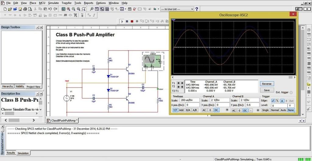
43 STEP 11 : example for class B Push pull amplifier circuit, Step 12. After designing circuit, To simulate circuit click Run in Simulate

44 Step 13 : To see output, click in CRO to see output, Step 14 : for example netlist for class B push pull amplifier look likes 44

45 Step 15 : You can run circuit by design NETLIST in report option,to see netlist click reports - netlist
46 GUIDELINES FOR DESIGNING CIRCUITS IN PSPICE Step 1 : Open ORCAD PSPICE Software Step 2: ORCAD main window 46

47 Step 3: Choose File menu ->new->project Step 4 : choose project name
48 Step 5 : select project using Analog or mixed A/D STEP 6 : Choose create blank project 48


49 Step 7 : ORCAD capture PCB Layout pin diagram opens Step 8 : choose place->part-to choose components

50 Step 9 : choose Add library to add component library files Step 10 : Add all files to main memory by selecting all 50
51 STEP 11 : Choose category from Library and select part list for to choose different elements Step 12 : for example to choose capacitor, select Analog from library and click C in part list. You can see preview of component in left side to confirm it. Step 13 : to select V DC source choose source from library and select it from part list, you can change it values

52 Step 14 : Right click in component and -> edit ->display properties-> change value 52

53 Step 15: to search particular component,select part search ->type name in part name Step 16 : After selecting component,place it in layout design, Step 17 : connecting two components using wire by selecting wire in parts,

54 Step 18 : to construct D TO A converter,we need resistors and capacitors. after selecting components and wire connection it look likes, Step 19 : to select already designed projects, choose file->open->design->browse stored folder. 54

55 After click file->design sources->schematic->page1 to view designed circuits Step 20 : Example to view Differential amplifier circuit, Step 21 : Example for Class B Push Pull Amplifier circuit,


56 Step 22 : To run simulation choose Run option and simulate Step 23 : you can see output in CRO by selecting from parts and place it where you have to see output 56
57
58 CIRCUIT DIAGRAM: VCC 5V Transformer R1 1kΩ L2 1mH L1 1mH C2 1µF C1 1µF U1 Output R2 1kΩ Q 2N2219 R3 1kΩ C3 1µF Ex. no: Date: SPICE SIMULATION OF TUNED COLLECTOR OSCILLATOR Aim: To simulate a Tuned collector oscillator circuit and to plot the frequency response characteristics. Apparatus required : i)personal Computer ii) SPICE (PSPICE 9.0 v& above or MULTISIM 10.0 v & above) Software. Procedure: i) Draw the circuit diagram after loading components from library. ii) A DC source with 0 V is place as the dummy voltage source to obtain the current waveform. iii) Wiring and proper net assignment has been made. The circuit is preprocessed. The VI characteristics may be obtained by performing DC transfer function Analysis. Place the current waveform marker at the positive terminal of the dummy voltage source (voltage =0 volts). Iv) For placing waveform markers, select tools instruments set wave form conent current waveform click on the required net and place the waveform marker.the sweep parameter (voltage) for input source is set in the Analysis window. V) The applied voltage is swept from an initial value to final value with the steps provided To get VI characteristics, the currents corresponding to varying input voltages are noted. vi) The VI graph is observed in the Waveform Viewer Result : Thus the Tuned collector oscillator is simulated successfully. 58
59 Circuit Diagram : WEIN BRIDGE OSCILLATOR VCC 5V R5 1kΩ R8 1kΩ R7 1kΩ R10 1kΩ C2 750nF R2 1kΩ R1 Tank circuit R3 1kΩ C3 750nF U1 C4 U2 750nF 1kΩ C1 750nF R4 1kΩ R6 1kΩ BC107BP R9 1kΩ BC107BP R11 1kΩ C5 750nF Output TWIN T OSCILLATOR:
60 Ex. no: Date: SPICE SIMULATION OF WEIN BRIDGE AND TWIN T OSCILLATOR Aim: To simulate a Wein Bridge and Twin T oscillator circuit and to plot the frequency response characteristics. Apparatus required : i)personal Computer ii) SPICE (PSPICE 9.0 v& above or MULTISIM 10.0 v & above) Software. Procedure: i) Draw the circuit diagram after loading components from library. ii) A DC source with 0 V is place as the dummy voltage source to obtain the current waveform. iii) Wiring and proper net assignment has been made. The circuit is preprocessed. The VI characteristics may be obtained by performing DC transfer function Analysis. Place the current waveform marker at the positive terminal of the dummy voltage source (voltage =0 volts). Iv) For placing waveform markers, select tools instruments set wave form conent current waveform click on the required net and place the waveform marker. The sweep parameter (voltage) for input source is set in the Analysis window. V) The applied voltage is swept from an initial value to final value with the steps provided To get VI characteristics, the currents corresponding to varying input voltages are noted. vi) The VI graph is observed in the Waveform Viewer. Result : Thus the Wein Bridge and Twin T oscillator circuit is simulated successfully. 60
61 CIRCUIT DIAGRAM: DOUBLE TUNED AMPLIFIER V1 12 V C3 T1 C4 C2 R1 1mΩ 30pF Key=A 50% NLT_PQ_4_10 U1 30pF Key=A 40% R4 1mΩ Output 750nF V2 BC107BP 120 Vrms 60 Hz 0 R2 1mΩ R3 1mΩ C1 750nF STAGGER TUNED AMPLIFIER VCC 5V C1 R1 1mΩ C3 L1 750nF 1mH C5 750nF U1 R3 1mΩ C6 750nF U2 L2 1mH C7 750nF Output 750nF R2 1mΩ BC107BP R6 1mΩ C2 750nF R4 1mΩ BC107BP R5 1mΩ C4 750nF
62 Ex. no: Date: SPICE SIMULATION OF DOUBLE AND STAGGER TUNED AMPLIFIERS Aim: To simulate a Double and Stagger tuned Amplifiers circuit and to plot the frequency response characteristics. Apparatus required : i) Personal Computer ii) SPICE (PSPICE 9.0 v& above or MULTISIM 10.0 v & above) Software. Procedure: i) Draw the circuit diagram after loading components from library. ii) A DC source with 0 V is place as the dummy voltage source to obtain the current waveform. iii) Wiring and proper net assignment has been made. The circuit is preprocessed. The VI characteristics may be obtained by performing DC transfer function Analysis. Place the current waveform marker at the positive terminal of the dummy voltage source (voltage =0 volts). Iv) For placing waveform markers, select tools instruments set wave form conent current waveform click on the required net and place the waveform marker.the sweep parameter (voltage) for input source is set in the Analysis window. V) The applied voltage is swept from an initial value to final value with the steps provided To get VI characteristics, the currents corresponding to varying input voltages are noted. vi) The VI graph is observed in the Waveform Viewer Result : Thus the Double and Stagger tuned Amplifier were simulated successfully. 62
63 CIRCUIT DIAGRAM: Ex. no: Date: Aim: BI STABLE MULTIVIBRATOR SPICE SIMULATION OF BI STABLE MULTIVIBRATOR To simulate a Bistable Multivibrator circuit and to plot the frequency response characteristics. Apparatus required : i) Personal Computer ii) SPICE (PSPICE 9.0 v& above or MULTISIM 10.0 v & above) Software. Procedure: i) Draw the circuit diagram after loading components from library. ii) A DC source with 0 V is place as the dummy voltage source to obtain the current waveform. iii) Wiring and proper net assignment has been made. The circuit is preprocessed. The VI characteristics may be obtained by performing DC transfer function Analysis. Place the current waveform marker at the positive terminal of the dummy voltage source (voltage =0 volts). Iv) For placing waveform markers, select tools instruments set wave form conent current waveform click on the required net and place the waveform marker.the sweep parameter (voltage) for input source is set in the Analysis window. V) The applied voltage is swept from an initial value to final value with the steps provided To get VI characteristics, the currents corresponding to varying input voltages are noted. vi) The VI graph is observed in the Waveform Viewer Result : Thus the Bistable Multivibrator was simulated successfully.
64 CIRCUIT DIAGRAM: SCHMITT TRIGGER Ex. no: Date: Aim: SPICE SIMULATION OF SCHMITT TRIGGER To simulate a Schmitt trigger circuit and to plot the frequency response characteristics. Apparatus required : i) Personal Computer ii) SPICE (PSPICE 9.0 v& above or MULTISIM 10.0 v & above) Software. Procedure: i) Draw the circuit diagram after loading components from library. ii) A DC source with 0 V is place as the dummy voltage source to obtain the current waveform. iii) Wiring and proper net assignment has been made. The circuit is preprocessed. The VI characteristics may be obtained by performing DC transfer function Analysis. Place the current waveform marker at the positive terminal of the dummy voltage source (voltage =0 volts). Iv) For placing waveform markers, select tools instruments set wave form conent current waveform click on the required net and place the waveform marker.the sweep parameter (voltage) for input source is set in the Analysis window. V) The applied voltage is swept from an initial value to final value with the steps provided To get VI characteristics, the currents corresponding to varying input voltages are noted. vi) The VI graph is observed in the Waveform Viewer Result : Thus the Schmitt Trigger was simulated successfully. 64
65 CIRCUIT DIAGRAM: Ex. no: Date: Aim: MONO STABLE MULTIVIBRATO SPICE SIMULATION OF MONO STABLE MULTIVIBRATOR To simulate a Mono stable Multivibrator circuit and to plot the output characteristics. Apparatus required : i) Personal Computer ii) SPICE (PSPICE 9.0 v& above or MULTISIM 10.0 v & above) Software. Procedure: i) Draw the circuit diagram after loading components from library. ii) A DC source with 0 V is place as the dummy voltage source to obtain the current waveform. iii) Wiring and proper net assignment has been made. The circuit is preprocessed. The VI characteristics may be obtained by performing DC transfer function Analysis. Place the current waveform marker at the positive terminal of the dummy voltage source (voltage =0 volts). Iv) For placing waveform markers, select tools instruments set wave form conent current waveform click on the required net and place the waveform marker.the sweep parameter (voltage) for input source is set in the Analysis window. V) The applied voltage is swept from an initial value to final value with the steps provided To get VI characteristics, the currents corresponding to varying input voltages are noted. vi) The VI graph is observed in the Waveform Viewer Result : Thus the Mono stable multivibrator was simulated successfully
66 CIRCUIT DIAGRAM: Ex. no: Date: Aim: CURRENT TIME BASE GENERATORS SPICE SIMULATION OF CURRENT TIME BASE GENERATORS To simulate a Current time base circuit and to plot the output characteristics. Apparatus required : i) Personal Computer ii) SPICE (PSPICE 9.0 v& above or MULTISIM 10.0 v & above) Software. Procedure: i) Draw the circuit diagram after loading components from library. ii) A DC source with 0 V is place as the dummy voltage source to obtain the current waveform. iii) Wiring and proper net assignment has been made. The circuit is preprocessed. The VI characteristics may be obtained by performing DC transfer function Analysis. Place the current waveform marker at the positive terminal of the dummy voltage source (voltage =0 volts). Iv) For placing waveform markers, select tools instruments set wave form conent current waveform click on the required net and place the waveform marker.the sweep parameter (voltage) for input source is set in the Analysis window. V) The applied voltage is swept from an initial value to final value with the steps provided To get VI characteristics, the currents corresponding to varying input voltages are noted. Result : Thus the Current time base circuit was simulated successfully. 66
DMI COLLEGE OF ENGINEERING
 DMI COLLEGE OF ENGINEERING PALANCHUR CHENNAI - 600123 DEPARTMENT OF ELECTRONICS AND COMMUNICATION ENGINEERING LABORATORY MANUAL SUB CODE SUBJECT TITLE SEMESTER YEAR DEPARTMENT : EC8461 : CIRCUITS DESIGN
Lab 4 : Transistor Oscillators
 Objective: Lab 4 : Transistor Oscillators In this lab, you will learn how to design and implement a colpitts oscillator. In part II you will implement a RC phase shift oscillator Hardware Required : Pre
Dharmapuri LAB MANUAL : B.E. ECE. Branch EC CIRCUITS AND SIMULATION INTEGRATED LABORATORY ICAL ENG
 Dharmapuri 636 703 LAB MANUAL Regulation : 203 Branch : B.E. ECE Year & Semester : II Year / IV Semester EC64 - CIRCUITS AND SIMULATION INTEGRATED LABORATORY ICAL ENG 2 ANNA UNIVERSITY CHENNAI Regulation
EC202- ELECTRONIC CIRCUITS II Unit- I -FEEEDBACK AMPLIFIER
 EC202- ELECTRONIC CIRCUITS II Unit- I -FEEEDBACK AMPLIFIER 1. What is feedback? What are the types of feedback? 2. Define positive feedback. What are its merits and demerits? 3. Define negative feedback.
For input: Peak to peak amplitude of the input = volts. Time period for 1 full cycle = sec
 Inverting amplifier: [Closed Loop Configuration] Design: A CL = V o /V in = - R f / R in ; Assume R in = ; Gain = ; Circuit Diagram: RF +10V F.G ~ + Rin 2 3 7 IC741 + 4 6 v0-10v CRO Model Graph Inverting
 RAJALAKSHMI ENGINEERING COLLEGE THANDALAM 602 105. DEPARTMENT OF ECE LAB MANUAL CLASS : II YEAR ECE SEMESTER : IV SEM (DEC 2009) SUBJECT CODE : EC2258 SUBJECT : LINEAR INTEGRATED CIRCUITS LAB PREPARED
LIC & COMMUNICATION LAB MANUAL
 LIC & Communication Lab Manual LIC & COMMUNICATION LAB MANUAL FOR V SEMESTER B.E (E& ( E&C) (For private circulation only) NAME: DEPARTMENT OF ELECTRONICS & COMMUNICATION SRI SIDDHARTHA INSTITUTE OF TECHNOLOGY
ANALOG ELECTRONIC CIRCUITS LABORATORY MANUAL (CODE: EEE - 228)
") ANALOG ELECTRONIC CIRCUITS LABORATORY MANUAL (CODE: EEE - 228) DEPARTMENT OF ELECTRONICS & COMMUNICATION ENGINEERING ANIL NEERUKONDA INSTITUTE OF TECHNOLOGY & SCIENCES (Affiliated to AU, Approved by AICTE
ANALOG ELECTRONIC CIRCUITS LABORATORY MANUAL (CODE: EEE - 228) DEPARTMENT OF ELECTRONICS & COMMUNICATION ENGINEERING ANIL NEERUKONDA INSTITUTE OF TECHNOLOGY & SCIENCES (Affiliated to AU, Approved by AICTE
BHARATHIDASAN ENGINEERING COLLEGE
 BHARATHIDASAN ENGINEERING COLLEGE DEPARTMENT OF ELECTRONICS AND COMMUNICATION ENGINEERING EC6401 - ELECTRONIC CIRCUITS - II QUESTION BANK II- YEAR IV SEM ACDEMIC YEAR: 2016-2017 EVEN SEMESTER EC6401 ELECTRONIC
VALLIAMMAI ENGINEERING COLLEGE
 VALLIAMMAI ENGINEERING COLLEGE SRM Nagar, Kattankulathur 603 203 DEPARTMENT OF ELECTRONICS AND COMMUNICATION ENGINEERING QUESTION BANK IV SEMESTER EC6401 ELECTRONICS CIRCUITS-II Regulation 2013 Academic
VALLIAMMAI ENGINEERING COLLEGE
 VALLIAMMAI ENGINEERING COLLEGE SRM Nagar, Kattankulathur 603 203. DEPARTMENT OF ELECTRONICS & COMMUNICATION ENGINEERING SUBJECT QUESTION BANK : EC6401 ELECTRONICS CIRCUITS-II SEM / YEAR: IV / II year B.E.
UNIT 1 MULTI STAGE AMPLIFIES
 UNIT 1 MULTI STAGE AMPLIFIES 1. a) Derive the equation for the overall voltage gain of a multistage amplifier in terms of the individual voltage gains. b) what are the multi-stage amplifiers? 2. Describe
Dev Bhoomi Institute Of Technology Department of Electronics and Communication Engineering PRACTICAL INSTRUCTION SHEET REV. NO. : REV.
 Dev Bhoomi Institute Of Technology Department of Electronics and Communication Engineering PRACTICAL INSTRUCTION SHEET LABORATORY MANUAL EXPERIMENT NO. ISSUE NO. : ISSUE DATE: July 200 REV. NO. : REV.
ELECTRONIC DEVICES AND CIRCUITS (EDC) LABORATORY MANUAL
 LABORATORY MANUAL") ELECTRONIC DEVICES AND CIRCUITS (EDC) LABORATORY MANUAL (B.E. THIRD SEMESTER - BEENE302P / BEECE302P/ BEETE302P) Prepared by Prof. S. Irfan Ali HOD PROF. M. NASIRUDDIN DEPARTMENT OF ELECTRONICS & TELECOMMUNICATION
ELECTRONIC DEVICES AND CIRCUITS (EDC) LABORATORY MANUAL (B.E. THIRD SEMESTER - BEENE302P / BEECE302P/ BEETE302P) Prepared by Prof. S. Irfan Ali HOD PROF. M. NASIRUDDIN DEPARTMENT OF ELECTRONICS & TELECOMMUNICATION
1. LINEAR WAVE SHAPING
 Aim: 1. LINEAR WAVE SHAPING i) To design a low pass RC circuit for the given cutoff frequency and obtain its frequency response. ii) To observe the response of the designed low pass RC circuit for the
Facility of Engineering. Biomedical Engineering Department. Medical Electronic Lab BME (317) Post-lab Forms
 Post-lab Forms") Facility of Engineering Biomedical Engineering Department Medical Electronic Lab BME (317) Post-lab Forms Prepared by Eng.Hala Amari Spring 2014 Facility of Engineering Biomedical Engineering Department
Facility of Engineering Biomedical Engineering Department Medical Electronic Lab BME (317) Post-lab Forms Prepared by Eng.Hala Amari Spring 2014 Facility of Engineering Biomedical Engineering Department
Facility of Engineering. Biomedical Engineering Department. Medical Electronic Lab BME (317) Pre-Report Forms
 Pre-Report Forms") Facility of Engineering Biomedical Engineering Department Medical Electronic Lab BME (317) Pre-Report Forms Prepared by Eng.Hala Amari Spring 2014 Facility of Engineering Biomedical Engineering Department
Facility of Engineering Biomedical Engineering Department Medical Electronic Lab BME (317) Pre-Report Forms Prepared by Eng.Hala Amari Spring 2014 Facility of Engineering Biomedical Engineering Department
Dev Bhoomi Institute Of Technology Department of Electronics and Communication Engineering PRACTICAL INSTRUCTION SHEET
 Dev Bhoomi Institute Of Technology Department of Electronics and Communication Engineering PRACTICAL INSTRUCTION SHEET LABORATORY MANUAL EXPERIMENT NO. ISSUE NO. : ISSUE DATE: REV. NO. : REV. DATE : PAGE:
LINEAR IC APPLICATIONS
 1 B.Tech III Year I Semester (R09) Regular & Supplementary Examinations December/January 2013/14 1 (a) Why is R e in an emitter-coupled differential amplifier replaced by a constant current source? (b)
INSTITUTE OF AERONAUTICAL ENGINERING DUNDIGAL, HYDERABAD
 INSTITUTE OF AERONAUTICAL ENGINERING DUNDIGAL, HYDERABAD 500 043 Digital Signal Processing Lab Work Book Name: Reg.No: Branch: Class: Section: IARE-ECE Department CERTIFICATE This is to certify that it
ELECTRONIC CIRCUITS LAB
 ELECTRONIC CIRCUITS LAB 1 2 STATE INSTITUTE OF TECHNICAL TEACHERS TRAINING AND RESEARCH GENERAL INSTRUCTIONS Rough record and Fair record are needed to record the experiments conducted in the laboratory.
Analog Electronics Laboratory
 Circuit Diagram a) Center tap FWR without filter b) Center tap FWR with C filter AC Supply AC Supply D2 c) Bridge Rectifier without filter d) Bridge Rectifier with C filter AC Supply AC Supply Waveforms
UNIVERSITY OF NORTH CAROLINA AT CHARLOTTE Department of Electrical and Computer Engineering
 UNIVERSITY OF NORTH CAROLINA AT CHARLOTTE Department of Electrical and Computer Engineering EXPERIMENT 7 BJT AMPLIFIER CONFIGURATIONS AND INPUT/OUTPUT IMPEDANCE OBJECTIVES The purpose of this experiment
 SET - 1 1. a) Write the application of attenuator b) State the clamping theorem c) Write the application of Monostable multi vibrator d) Draw the diagram for Diode two input AND gate e) Define the terms
CHADALAWADA RAMANAMMA ENGINEERING COLLEGE (AUTONOMOUS) Chadalawada Nagar, Renigunta Road, Tirupati
 Chadalawada Nagar, Renigunta Road, Tirupati") IC APPLICATIONS LABORATORY MANUAL Subject Code : 15A04507 Regulations : R15 Class : V Semester (ECE) CHADALAWADA RAMANAMMA ENGINEERING COLLEGE (AUTONOMOUS) Chadalawada Nagar, Renigunta Road, Tirupati 517
IC APPLICATIONS LABORATORY MANUAL Subject Code : 15A04507 Regulations : R15 Class : V Semester (ECE) CHADALAWADA RAMANAMMA ENGINEERING COLLEGE (AUTONOMOUS) Chadalawada Nagar, Renigunta Road, Tirupati 517
EXPT NO: 1.A. COMMON EMITTER AMPLIFIER (Software) PRELAB:
 PRELAB:") EXPT NO: 1.A COMMON EMITTER AMPLIFIER (Software) PRELAB: 1. Study the operation and working principle of CE amplifier. 2. Identify all the formulae you will need in this Lab. 3. Study the procedure of
EXPT NO: 1.A COMMON EMITTER AMPLIFIER (Software) PRELAB: 1. Study the operation and working principle of CE amplifier. 2. Identify all the formulae you will need in this Lab. 3. Study the procedure of
Analog Electronic Circuits Lab-manual
 2014 Analog Electronic Circuits Lab-manual Prof. Dr Tahir Izhar University of Engineering & Technology LAHORE 1/09/2014 Contents Experiment-1:...4 Learning to use the multimeter for checking and indentifying
DHANALAKSHMI COLLEGE OF ENGINEERING DEPARTMENT OF ELECTRICAL AND ELECTRONICS ENGINEERING EC6202 ELECTRONIC DEVICES AND CIRCUITS
 DHANALAKSHMI COLLEGE OF ENGINEERING DEPARTMENT OF ELECTRICAL AND ELECTRONICS ENGINEERING EC6202 ELECTRONIC DEVICES AND CIRCUITS UNIT-I - PN DIODEAND ITSAPPLICATIONS 1. What is depletion region in PN junction?
CIRCUIT DIAGRAM Half Wave Rectifier. Half Wave Rectifier with filter 2012/ODD/III/ECE/EC I/LM 1
 CIRCUIT DIAGRAM Half Wave Rectifier Half Wave Rectifier with filter 2012/ODD/III/ECE/EC I/LM 1 Ex.No. 1 Date: / /2012 Power supply circuit using Half Wave rectifiers AIM To Build and understand the operation
Government Polytechnic Muzaffarpur Name of the Lab: Applied Electronics Lab
 Government Polytechnic Muzaffarpur Name of the Lab: Applied Electronics Lab Subject Code: 1620408 Experiment-1 Aim: To obtain the characteristics of field effect transistor (FET). Theory: The Field Effect
Question Bank EC6401 ELECTRONIC CIRCUITS - II
 FATIMA MICHAEL COLLEGE OF ENGINEERING & TECHNOLOGY Madurai Sivagangai Main Road Madurai - 625 020. [An ISO 9001:2008 Certified Institution] SEMESTER: IV / ECE Question Bank EC6401 ELECTRONIC CIRCUITS -
WAVEFORM GENERATOR CIRCUITS USING OPERATIONAL AMPLIFIERS
 15EEE287 Electronic Circuits & Simulation Lab - II Lab #8 WAVEFORM GENERATOR CIRCUITS USING OPERATIONAL AMPLIFIERS OBJECTIVE The purpose of the experiment is to design and construct circuits to generate
EE301 ELECTRONIC CIRCUITS CHAPTER 2 : OSCILLATORS. Lecturer : Engr. Muhammad Muizz Bin Mohd Nawawi
 EE301 ELECTRONIC CIRCUITS CHAPTER 2 : OSCILLATORS Lecturer : Engr. Muhammad Muizz Bin Mohd Nawawi 2.1 INTRODUCTION An electronic circuit which is designed to generate a periodic waveform continuously at
SIDDHARTH GROUP OF INSTITUTIONS :: PUTTUR (AUTONOMOUS) Siddharth Nagar, Narayanavanam Road QUESTION BANK
 Siddharth Nagar, Narayanavanam Road QUESTION BANK") SIDDHARTH GROUP OF INSTITUTIONS :: PUTTUR (AUTONOMOUS) Siddharth Nagar, Narayanavanam Road 517583 QUESTION BANK Subject with Code : Electronic Circuit Analysis (16EC407) Year & Sem: II-B.Tech & II-Sem
SIDDHARTH GROUP OF INSTITUTIONS :: PUTTUR (AUTONOMOUS) Siddharth Nagar, Narayanavanam Road 517583 QUESTION BANK Subject with Code : Electronic Circuit Analysis (16EC407) Year & Sem: II-B.Tech & II-Sem
LAB MANUAL EC6412- LINEAR INTEGRATED CIRCUIT LABORATORY. Dharmapuri Regulation : 2013 Branch : B.E. ECE
 EC6412 LINEAR INTEGRATED CIRCUITS LABORATORY 1 Dharmapuri 636 703 LAB MANUAL Regulation : 2013 Branch Year & Semester : B.E. ECE : II Year / IV Semester EC6412- LINEAR INTEGRATED CIRCUIT LABORATORY EC6412
ANALOG ELECTRONIC CIRCUITS (EE-325-F) LAB MANUAL
 LAB MANUAL") ANALOG ELECTRONIC CIRCUITS (EE-325-F) LAB MANUAL V SEMESTER Department Of Electronics & CommunicationEngg. BSA Institute of Technology & Management Faridabad. LIST OF EXPERIMENTS S.NO. NAME OF THE EXPERIMENT
ANALOG ELECTRONIC CIRCUITS (EE-325-F) LAB MANUAL V SEMESTER Department Of Electronics & CommunicationEngg. BSA Institute of Technology & Management Faridabad. LIST OF EXPERIMENTS S.NO. NAME OF THE EXPERIMENT
Sub Code & Name: EC2251- ELECTRONIC CIRCUITS II Unit : I Branch : ECE Year:II
 Unit : I Branch : ECE Year:II Page 01 of 06 UNIT 1 FEEDBACK AMPLIFIERS 9 Block diagram, Loop gain, Gain with feedback, Effects of negative feedback Sensitivity and desensitivity of gain, Cut-off frequencies,
GOVERNMENT OF KARNATAKA KARNATAKA STATE PRE-UNIVERSITY EDUCATION EXAMINATION BOARD II YEAR PUC EXAMINATION MARCH-2012 SCHEME OF VALUATION
 GOVERNMENT OF KARNATAKA KARNATAKA STATE PRE-UNIVERSITY EDUCATION EXAMINATION BOARD II YEAR PUC EXAMINATION MARCH-0 SCHEME OF VALUATION Subject Code: 0 Subject: Qn. PART - A 0. Which is the largest of three
FREQUENTLY ASKED QUESTIONS
 FREQUENTLY ASKED QUESTIONS UNIT-1 SUBJECT : ELECTRONIC DEVICES AND CIRCUITS SUBJECT CODE : EC6202 BRANCH: EEE PART -A 1. What is meant by diffusion current in a semi conductor? (APR/MAY 2010, 2011, NOV/DEC
GATE: Electronics MCQs (Practice Test 1 of 13)
") GATE: Electronics MCQs (Practice Test 1 of 13) 1. Removing bypass capacitor across the emitter leg resistor in a CE amplifier causes a. increase in current gain b. decrease in current gain c. increase
GATE: Electronics MCQs (Practice Test 1 of 13) 1. Removing bypass capacitor across the emitter leg resistor in a CE amplifier causes a. increase in current gain b. decrease in current gain c. increase
ST.ANNE S COLLEGE OF ENGINEERING AND TECHNOLOGY ANGUCHETTYPALAYAM, PANRUTI Department of Electronics & Communication Engineering OBSERVATION
 ST.ANNE S COLLEGE OF ENGINEERING AND TECHNOLOGY ANGUCHETTYPALAYAM, PANRUTI 67 Department of Electronics & Communication Engineering OBSERVATION EC836 ANALOG AND DIGITAL CIRCUITS LABORATORY STUDENT NAME
Analog Circuit II Laboratory ( EC 409) EC 409 Analog Electronics Lab - II
 EC 409 Analog Electronics Lab - II") Analog Circuit II Laboratory ( EC 409) Subject Subject Title L T P Contact Credit Full Code Hours / Unit# Marks EC 409 Analog Electronics Lab - II 0 0 2 2 1 100 Course Outcomes:- After successful completion
Analog Circuit II Laboratory ( EC 409) Subject Subject Title L T P Contact Credit Full Code Hours / Unit# Marks EC 409 Analog Electronics Lab - II 0 0 2 2 1 100 Course Outcomes:- After successful completion
State the application of negative feedback and positive feedback (one in each case)
") (ISO/IEC - 700-005 Certified) Subject Code: 073 Model wer Page No: / N Important Instructions to examiners: ) The answers should be examined by key words and not as word-to-word as given in the model answer
(ISO/IEC - 700-005 Certified) Subject Code: 073 Model wer Page No: / N Important Instructions to examiners: ) The answers should be examined by key words and not as word-to-word as given in the model answer
THIRD SEMESTER ELECTRONICS - II BASIC ELECTRICAL & ELECTRONICS LAB DEPARTMENT OF ELECTRICAL ENGINEERING
 THIRD SEMESTER ELECTRONICS - II BASIC ELECTRICAL & ELECTRONICS LAB DEPARTMENT OF ELECTRICAL ENGINEERING Prepared By: Checked By: Approved By: Engr. Saqib Riaz Engr. M.Nasim Khan Dr.Noman Jafri Lecturer
Code: 9A Answer any FIVE questions All questions carry equal marks *****
 II B. Tech II Semester (R09) Regular & Supplementary Examinations, April/May 2012 ELECTRONIC CIRCUIT ANALYSIS (Common to EIE, E. Con. E & ECE) Time: 3 hours Max Marks: 70 Answer any FIVE questions All
ELC224 Final Review (12/10/2009) Name:
 Name:") ELC224 Final Review (12/10/2009) Name: Select the correct answer to the problems 1 through 20. 1. A common-emitter amplifier that uses direct coupling is an example of a dc amplifier. 2. The frequency
ELC224 Final Review (12/10/2009) Name: Select the correct answer to the problems 1 through 20. 1. A common-emitter amplifier that uses direct coupling is an example of a dc amplifier. 2. The frequency
BJT Circuits (MCQs of Moderate Complexity)
") BJT Circuits (MCQs of Moderate Complexity) 1. The current ib through base of a silicon npn transistor is 1+0.1 cos (1000πt) ma. At 300K, the rπ in the small signal model of the transistor is i b B C r
BJT Circuits (MCQs of Moderate Complexity) 1. The current ib through base of a silicon npn transistor is 1+0.1 cos (1000πt) ma. At 300K, the rπ in the small signal model of the transistor is i b B C r
GOVERNMENT OF KARNATAKA KARNATAKA STATE PRE-UNIVERSITY EDUCATION EXAMINATION BOARD II YEAR PUC EXAMINATION JULY-2012 SCHEME OF VALUATION
 GOVERNMENT OF KARNATAKA KARNATAKA STATE PRE-UNIVERSITY EDUCATION EXAMINATION BOARD II YEAR PUC EXAMINATION JULY-0 SCHEME OF VALUATION Subject Code: 40 Subject: PART - A 0. Which region of the transistor
Document Name: Electronic Circuits Lab. Facebook: Twitter:
 Document Name: Electronic Circuits Lab www.vidyathiplus.in Facebook: www.facebook.com/vidyarthiplus Twitter: www.twitter.com/vidyarthiplus Copyright 2011-2015 Vidyarthiplus.in (VP Group) Page 1 CIRCUIT
Dr.NNCE ECE/IVSEM LIC LAB-LM
 EC2258 - LINEAR INTEGRATED CIRCUITS LABORATORY LABORATORY MANUAL FOR IV SEMESTER B.E (ECE) ACADEMIC YEAR(2013-2014) (FOR PRIVATE CIRCULATION ONLY) ANNA UNIVERSITY CHENNAI-600 025 (REGULATION 2008) DEPARTMENT
Lab 2: Discrete BJT Op-Amps (Part I)
") Lab 2: Discrete BJT Op-Amps (Part I) This is a three-week laboratory. You are required to write only one lab report for all parts of this experiment. 1.0. INTRODUCTION In this lab, we will introduce and
Lab 2: Discrete BJT Op-Amps (Part I) This is a three-week laboratory. You are required to write only one lab report for all parts of this experiment. 1.0. INTRODUCTION In this lab, we will introduce and
 EC 6411 CIRCUITS AND SIMULATION INTEGRATED LABORATORY LABORATORY MANUAL INDEX EXPT.NO NAME OF THE EXPERIMENT PAGE NO 1 HALF WAVE AND FULL WAVE RECTIFIER 3 2 FIXED BIAS AMPLIFIER CIRCUIT USING BJT 3 BJT
GATE SOLVED PAPER - IN
 YEAR 202 ONE MARK Q. The i-v characteristics of the diode in the circuit given below are : v -. A v 0.7 V i 500 07 $ = * 0 A, v < 0.7 V The current in the circuit is (A) 0 ma (C) 6.67 ma (B) 9.3 ma (D)
FREQUENCY RESPONSE OF COMMON COLLECTOR AMPLIFIER
 Exp. No #5 FREQUENCY RESPONSE OF COMMON COLLECTOR AMPLIFIER Date: OBJECTIVE The purpose of the experiment is to analyze and plot the frequency response of a common collector amplifier. EQUIPMENT AND COMPONENTS
R05. For the circuit shown in fig.1, a sinusoidal voltage of peak 75V is applied. Assume ideal diodes. Obtain the output waveforms.
 Code.No: 33051 R05 SET-1 JAWAHARLAL NEHRU TECHNOLOGICAL UNIVERSITY HYDERABAD II.B.TECH - I SEMESTER SUPPLEMENTARY EXAMINATIONS NOVEMBER, 2009 (Common to EEE, ECE, EIE, ETM) Time: 3hours Max.Marks:80 Answer
15EEE282 Electronic Circuits and Simulation Lab - I Lab # 6
 Exp. No #6 FREQUENCY RESPONSE OF COMMON EMITTER AMPLIFIER OBJECTIVE The purpose of the experiment is to design a common emitter amplifier. To analyze and plot the frequency response of the amplifier with
Summer 2015 Examination
 Summer 2015 Examination Subject Code: 17445 Model Answer Important Instructions to examiners: 1) The answers should be examined by key words and not as word-to-word as given in the model answer scheme.
AURORA S ENGINEERING COLLEGE BHONGIR, NALGONDA DIST
 AURORA S ENGINEERING COLLEGE BHONGIR, NALGONDA DIST. 508116. Lab manual of IC APPLICATIONS LAB 3 rd Year 1 st Sem. ECE 2014-15 DEPARTMENT OF ELECTRONICS AND COMMUNICATION ENGINEERING 1 PREFACE Integrated
Objective: To study and verify the functionality of a) PN junction diode in forward bias. Sl.No. Name Quantity Name Quantity 1 Diode
 PN junction diode in forward bias. Sl.No. Name Quantity Name Quantity 1 Diode") Experiment No: 1 Diode Characteristics Objective: To study and verify the functionality of a) PN junction diode in forward bias Components/ Equipments Required: b) Point-Contact diode in reverse bias Components
Experiment No: 1 Diode Characteristics Objective: To study and verify the functionality of a) PN junction diode in forward bias Components/ Equipments Required: b) Point-Contact diode in reverse bias Components
Oscillators. An oscillator may be described as a source of alternating voltage. It is different than amplifier.
 Oscillators An oscillator may be described as a source of alternating voltage. It is different than amplifier. An amplifier delivers an output signal whose waveform corresponds to the input signal but
R a) Explain the operation of RC high-pass circuit when exponential input is applied.
 Explain the operation of RC high-pass circuit when exponential input is applied.") SET - 1 1. a) Explain the operation of RC high-pass circuit when exponential input is applied. 2x V ( e 1) V b) Verify V2 = = tanhx for a symmetrical square wave applied to a RC low 2x 2 ( e + 2 pass circuit.
SET - 1 1. a) Explain the operation of RC high-pass circuit when exponential input is applied. 2x V ( e 1) V b) Verify V2 = = tanhx for a symmetrical square wave applied to a RC low 2x 2 ( e + 2 pass circuit.
SET - 1 Code No: II B. Tech II Semester Regular Examinations, April/May 2009
 SET - 1 Code No: 3220401 II B. Tech II Semester Regular Examinations, April/May 2009 PULSE AND DIGITAL CIRCUITS ( Common to E.C.E, B.M.E, E.Con.E, I.C.E ) Time: 3 hours Max Marks: 80 Answer Any FIVE Questions
Figure 1: Closed Loop System
 SIGNAL GENERATORS 3. Introduction Signal sources have a variety of applications including checking stage gain, frequency response, and alignment in receivers and in a wide range of other electronics equipment.
INSTITUTE OF AERONAUTICAL ENGINEERING (AUTONOMUS) Dundigal, Hyderabad
 Dundigal, Hyderabad") INSTITUTE OF AERONAUTICAL ENGINEERING (AUTONOMUS) Dundigal, Hyderabad - 00 0 ELECTRONICS AND COMMUNICATION ENGINEERING ASSIGNMENT Name : ELECTRONIC CIRCUIT ANALYSIS Code : A0 Class : II - B. Tech nd semester
INSTITUTE OF AERONAUTICAL ENGINEERING (AUTONOMUS) Dundigal, Hyderabad - 00 0 ELECTRONICS AND COMMUNICATION ENGINEERING ASSIGNMENT Name : ELECTRONIC CIRCUIT ANALYSIS Code : A0 Class : II - B. Tech nd semester
Chapter.8: Oscillators
 Chapter.8: Oscillators Objectives: To understand The basic operation of an Oscillator the working of low frequency oscillators RC phase shift oscillator Wien bridge Oscillator the working of tuned oscillator
NOORUL ISLAM COLLEGE OF ENGG, KUMARACOIL. DEPARTMENT OF ELECTRONICS AND COMMUNICATION ENGG. SUBJECT CODE: EC 1251 SUBJECT NAME: ELECTRONIC CIRCUITS-II
 NOORUL ISLAM COLLEGE OF ENGG, KUMARACOIL. DEPARTMENT OF ELECTRONICS AND COMMUNICATION ENGG. SUBJECT CODE: EC 1251 SUBJECT NAME: ELECTRONIC CIRCUITS-II Prepared by, C.P.SREE BALA LEKSHMI (Lect/ECE) ELECTRONICS
UNIT - 1 OPERATIONAL AMPLIFIER FUNDAMENTALS
 UNIT - 1 OPERATIONAL AMPLIFIER FUNDAMENTALS 1.1 Basic operational amplifier circuit- hte basic circuit of an operational amplifier is as shown in above fig. has a differential amplifier input stage and
Multivibrators. Department of Electrical & Electronics Engineering, Amrita School of Engineering
 Multivibrators Multivibrators Multivibrator is an electronic circuit that generates square, rectangular, pulse waveforms. Also called as nonlinear oscillators or function generators. Multivibrator is basically
FREQUENCY RESPONSE OF COMMON COLLECTOR AMPLIFIER
 Exp. No #6 FREQUENCY RESPONSE OF COMMON COLLECTOR AMPLIFIER OBJECTIVE The purpose of the experiment is to analyze and plot the frequency response of a common collector amplifier. EQUIPMENT AND COMPONENTS
Shankersinh Vaghela Bapu Institute of Technology INDEX
 Shankersinh Vaghela Bapu Institute of Technology Diploma EE Semester III 3330905: ELECTRONIC COMPONENTS AND CIRCUITS INDEX Sr. No. Title Page Date Sign Grade 1 Obtain I-V characteristic of Diode. 2 To
Department of Biomedical Engineering BME 317. Medical Electronics Lab
 Department of Biomedical Engineering BME 317 Medical Electronics Lab Modified by Dr.Husam AL.Hamad and Eng.Roba AL.Omari Summer 2009 Exp # Title Page 1 2 3 4 An Introduction To Basic Laboratory Equipments
II B.TECH - II SEM ECE
 NRI INSTITUTE OF TECHNOLOGY (Approved by AICTE, New Delhi: Affiliated to JNTUK, Kakinada) Accredited by NAAC A grade, POTHAVARAPPADU (V), (via) Nunna, Agiripalli (M), Krishna District, A.P. PIN: 521212
Lab 4. Transistor as an amplifier, part 2
 Lab 4 Transistor as an amplifier, part 2 INTRODUCTION We continue the bi-polar transistor experiments begun in the preceding experiment. In the common emitter amplifier experiment, you will learn techniques
Gechstudentszone.wordpress.com
 8.1 Operational Amplifier (Op-Amp) UNIT 8: Operational Amplifier An operational amplifier ("op-amp") is a DC-coupled high-gain electronic voltage amplifier with a differential input and, usually, a single-ended
Analog and Telecommunication Electronics
 Politecnico di Torino - ICT School Analog and Telecommunication Electronics A3 BJT Amplifiers»Biasing» Output dynamic range» Small signal analysis» Voltage gain» Frequency response 12/03/2012-1 ATLCE -
The steeper the phase shift as a function of frequency φ(ω) the more stable the frequency of oscillation
 the more stable the frequency of oscillation") It should be noted that the frequency of oscillation ω o is determined by the phase characteristics of the feedback loop. the loop oscillates at the frequency for which the phase is zero The steeper the
It should be noted that the frequency of oscillation ω o is determined by the phase characteristics of the feedback loop. the loop oscillates at the frequency for which the phase is zero The steeper the
OBJECTIVE TYPE QUESTIONS
 OBJECTIVE TYPE QUESTIONS Q.1 The breakdown mechanism in a lightly doped p-n junction under reverse biased condition is called (A) avalanche breakdown. (B) zener breakdown. (C) breakdown by tunnelling.
Skyup's Media ELECTRONIC CIRCUIT ANALYSIS
 ELECTRONIC CIRCUIT ANALYSIS MALLAREDDY COLLEGE OF ENGINEERING AND TECHNOLOGY DEPARTMENT OF ELECTROINICS AND COMMUNICATION ENGINEERING Answer all the following questions: PART A: B.TECH II YEAR II SEMESTER
 11. What is fall time (tf) in transistor? The time required for the collector current to fall from 90% to 10% of its DEPARTMENT OF ECE EC 6401 Electronic Circuits II UNIT-IV WAVE SHAPING AND MULTIVIBRATOR
Small signal Amplifier stages. Figure 5.2 Classification of power amplifiers
 5.1 Introduction When the power requirement to drive the load is in terms of several Watts rather than mili-watts the power amplifiers are used. Power amplifiers form the last stage of multistage amplifiers.
MARIA COLLEGE OF ENGINEERING AND TECHNOLOGY, ATTOOR UNIT-1. Feedback Amplifiers
 MARIA COLLEGE OF ENGINEERING AND TECHNOLOGY, ATTOOR DEPARTMENT OF ELECTRONICS AND COMMUNICATION ENGINEERING ELECTRONIC CIRCUITS-II 2 MARKS QUESTIONS & ANSWERS UNIT-1 Feedback Amplifiers 1. What is meant
Code No: R Set No. 1
 Code No: R059210404 Set No. 1 II B.Tech I Semester Supplimentary Examinations, February 2008 ELECTRONIC CIRCUIT ANALYSIS ( Common to Electronics & Communication Engineering and Electronics & Telematics)
A 3-STAGE 5W AUDIO AMPLIFIER
 ECE 2201 PRELAB 7x BJT APPLICATIONS A 3-STAGE 5W AUDIO AMPLIFIER UTILIZING NEGATIVE FEEDBACK INTRODUCTION Figure P7-1 shows a simplified schematic of a 3-stage audio amplifier utilizing three BJT amplifier
Linear electronic. Lecture No. 1
 1 Lecture No. 1 2 3 4 5 Lecture No. 2 6 7 8 9 10 11 Lecture No. 3 12 13 14 Lecture No. 4 Example: find Frequency response analysis for the circuit shown in figure below. Where R S =4kR B1 =8kR B2 =4k R
Function Generator Using Op Amp Ic 741 Theory
 Function Generator Using Op Amp Ic 741 Theory Note: Op-Amps ua741, LM 301, LM311, LM 324 & AD 633 may be used To design an Inverting Amplifier for the given specifications using Op-Amp IC 741. THEORY:
THE UNIVERSITY OF HONG KONG. Department of Electrical and Electrical Engineering
 THE UNIVERSITY OF HONG KONG Department of Electrical and Electrical Engineering Experiment EC1 The Common-Emitter Amplifier Location: Part I Laboratory CYC 102 Objective: To study the basic operation and
INTEGRATED CIRCUITS AND APPLICATIONS LAB MANUAL
 INTEGRATED CIRCUITS AND APPLICATIONS LAB MANUAL V SEMESTER Department of Electronics and communication Engineering Government Engineering College, Dahod-389151 http://www.gecdahod.ac.in/ L A B M A N U
INSTITUTE OF AERONAUTICAL ENGINEERING (Autonomous) Dundigal, Hyderabad
 Dundigal, Hyderabad") P a g e INSTITUTE OF AERONAUTICAL ENGINEERING (Autonomous) Dundigal, Hyderabad - 500 043 ELECTRONICS AND COMMUNICATION ENGINEERING TUTORIAL QUESTION BANK Name : PULSE AND DIGITAL CIRCIUTS Code : AEC006
P a g e INSTITUTE OF AERONAUTICAL ENGINEERING (Autonomous) Dundigal, Hyderabad - 500 043 ELECTRONICS AND COMMUNICATION ENGINEERING TUTORIAL QUESTION BANK Name : PULSE AND DIGITAL CIRCIUTS Code : AEC006
INSTITUTE OF AERONAUTICAL ENGINEERING (Autonomous) Dundigal, Hyderabad ELECTRICAL AND ELECTRONICS ENGINEERING
 Dundigal, Hyderabad ELECTRICAL AND ELECTRONICS ENGINEERING") INSTITUTE OF AERONAUTICAL ENGINEERING (Autonomous) Dundigal, Hyderabad - 500 043 ELECTRICAL AND ELECTRONICS ENGINEERING BANK Course Title Course Code Regulation Course Structure Course Coordinator Team
INSTITUTE OF AERONAUTICAL ENGINEERING (Autonomous) Dundigal, Hyderabad - 500 043 ELECTRICAL AND ELECTRONICS ENGINEERING BANK Course Title Course Code Regulation Course Structure Course Coordinator Team
UNIT 1. 9 What is the Causes of Free Response in Electrical Circuit. 12 Write the Expression for transient current and voltages of RL circuit.
 SUB: Electric Circuits and Electron Devices Course Code: UBEE309 UNIT 1 PART A 1 State Transient and Transient Time? 2 What is Tansient State? 3 What is Steady State? 4 Define Source Free Response 5 Define
LINEAR INTEGRATED CIRCUITS APPLICATIONS LABORATORY OBSERVATION
 LENDI INSTITUTE OF ENGINEERING AND TECHNOLOGY (Approved by A.I.C.T.E & Affiliated to JNTU, Kakinada) Jonnada (Village), Denkada (Mandal), Vizianagaram Dist 535005 Phone No. 08922-241111, 241112 E-Mail:
ECE 3274 Common-Emitter Amplifier Project
 ECE 3274 Common-Emitter Amplifier Project 1. Objective The objective of this lab is to design and build three variations of the common- emitter amplifier. 2. Components Qty Device 1 2N2222 BJT Transistor
EXPERIMENT 10: SINGLE-TRANSISTOR AMPLIFIERS 10/27/17
 EXPERIMENT 10: SINGLE-TRANSISTOR AMPLIFIERS 10/27/17 In this experiment we will measure the characteristics of the standard common emitter amplifier. We will use the 2N3904 npn transistor. If you have
15EI204L-ANALOG ELECTRONIC CIRCUITS LAB MANUAL
 15EI204L-ANALOG ELECTRONIC CIRCUITS LAB MANUAL Department of Electronics and Instrumentation Engineering Faculty of Engineering and Technology Department of Electronics and Instrumentation Engineering
The George Washington University School of Engineering and Applied Science Department of Electrical and Computer Engineering ECE 20 - LAB
 The George Washington University School of Engineering and Applied Science Department of Electrical and Computer Engineering ECE 20 - LAB Experiment # 6 (Part I) Bipolar Junction Transistors Common Emitter
MAHALAKSHMI ENGINEERING COLLEGE TIRUCHIRAPALLI
 MAHALAKSHMI ENGINEERING COLLEGE TIRUCHIRAPALLI-621213. QUESTION BANK DEPARTMENT: EEE SUBJECT CODE: EE2203 SEMESTER : III SUBJECT NAME: ELECTRONIC DEVICES &CIRCUITS UNIT 4-AMPLIFIERS AND OSCILLATORS PART
Scheme I Sample Question Paper
 Sample Question Paper Marks : 70 Time: 3 Hrs. Q.1) Attempt any FIVE of the following. 10 Marks a) Classify configuration of differential amplifier. b) Draw equivalent circuit of an OPAMP c) Suggest and
Scheme Q.1 Attempt any SIX of following: 12-Total Marks a) Draw symbol NPN and PNP transistor. 2 M Ans: Symbol Of NPN and PNP BJT (1M each)
 Draw symbol NPN and PNP transistor. 2 M Ans: Symbol Of NPN and PNP BJT (1M each)") Q. No. WINTER 16 EXAMINATION (Subject Code: 17319) Model Answer Important Instructions to examiners: 1) The answers should be examined by key words and not as word-to-word as given in the model answer
Q. No. WINTER 16 EXAMINATION (Subject Code: 17319) Model Answer Important Instructions to examiners: 1) The answers should be examined by key words and not as word-to-word as given in the model answer
Operating Manual Ver.1.1
 Common Collector Amplifier Operating Manual Ver.1.1 An ISO 9001 : 2000 company 94-101, Electronic Complex Pardesipura, Indore- 452010, India Tel : 91-731- 2570301/02, 4211100 Fax: 91-731- 2555643 e mail
EC6361 ELECTRONICS LABORATORY II YEAR- III SEMESTER
 EC6361 ELECTRONICS LABORATORY LAB MANUAL II YEAR- III SEMESTER LIST OF EXPERIMENTS 1. Characteristics of Semi conductor diode and Zener diode 2. Characteristics of a NPN Transistor under common emitter,