CAT Channel Fractional LED Driver in TQFN 3x3
|
|
|
- Erika Stone
- 6 years ago
- Views:
Transcription

1 6-Channel Fractional LED Driver in TQFN 3x3 Description The CAT3636 is a high efficiency fractional charge pump that can drive up to six LEDs programmable by a one wire digital interface. The inclusion of a 1.33x fractional charge pump mode increases device efficiency by up to 10% over traditional 1.5x charge pumps with no added external capacitors. Low noise input ripple is achieved by operating at a constant switching frequency which allows the use of small external ceramic capacitors. The multi fractional charge pump supports a wide range of input voltages from 2.5 V to 5.5 V. The EN/SET logic input functions as a chip enable and a 1 wire addressable interface for control and current setting of all LEDs. Three groups of two LEDs can be configured with independent LED currents between 0.25 ma and 32 ma. The device is available in a tiny 16 lead TQFN 3 mm x 3 mm package with a max height of 0.8 mm. ON Semiconductor s 1.33x charge pump switching architecture is patented. LEDC2 LEDC1 LEDB2 LEDB1 TQFN 16 HV3 SUFFIX CASE 510AD PIN CONNECTIONS 1 EN/S GND NC NC C2 C2+ C1 C1+ Features High Efficiency 1.33x Charge Pump Charge Pump: 1x, 1.33x, 1.5x, 2x Drives up to 6 LEDs at 32 ma Each 1 Wire EZDim LED Current Programming Power Efficiency up to 92% Low Noise Input Ripple in All Modes Zero Current Shutdown Mode Soft Start and Current Limiting Short Circuit Protection Thermal Shutdown Protection Tiny 3 mm x 3 mm, 16 lead TQFN Package These Devices are Pb Free, Halogen Free/BFR Free and are RoHS Compliant Applications LCD Display Backlight Color RGB LEDs Cellular Phones Digital Still Cameras Handheld Devices JAAA AXXX YWW LEDA2 LEDA1 VOUT VIN (Top View) MARKING DIAGRAMS ORDERING INFORMATION Device Package Shipping CAT3636HV3 T2 (Note 1) TQFN 16 (Pb Free) JAAR AXXX YWW JAAA = CAT3636HV3 T2 JAAR = CAT3636HV3 GT2 A = Assembly Location XXX = Last Three Digits of Assembly Lot Number Y = Production Year (Last Digit) WW = Production Week (Two Digits) CAT3636HV3 GT2 (Note 2) TQFN 16 (Pb Free) 2000/ Tape & Reel For information on tape and reel specifications, including part orientation and tape sizes, please refer to our Tape and Reel Packaging Specifications Brochure, BRD8011/D. 1. Matte Tin Plated Finish (RoHS compliant). 2. NiPdAu Plated Finish (RoHS compliant). Semiconductor Components Industries, LLC, 2014 August, 2014 Rev. 8 1 Publication Order Number: CAT3636/D
2 1 F 1 F V IN 2.5 V to 5.5 V CIN 1 F One wire programming C1 C1+ C2 C2+ VIN VOUT CAT3636 LEDA1 LEDA2 LEDB1 EN/SET LEDB2 LEDC1 GND LEDC2 pair A pair B pair C 1 F 20 ma C OUT Figure 1. Typical Application Circuit Table 1. ABSOLUTE MAXIMUM RATINGS Parameter Rating Unit VIN, LEDx, C1±, C2± voltage 6 V VOUT Voltage 7 V EN/SET Voltage VIN V V Storage Temperature Range 65 to +160 C Junction Temperature Range (Note 3) 40 to +150 C Lead Temperature 300 C Stresses exceeding those listed in the Maximum Ratings table may damage the device. If any of these limits are exceeded, device functionality should not be assumed, damage may occur and reliability may be affected. Table 2. RECOMMENDED OPERATING CONDITIONS Parameter Range Unit VIN 2.5 to 5.5 V Ambient Temperature Range (Note 3) 40 to +85 C I LED per LED pin 0 to 32 ma Total Output Current 0 to 192 ma Functional operation above the stresses listed in the Recommended Operating Ranges is not implied. Extended exposure to stresses beyond the Recommended Operating Ranges limits may affect device reliability. NOTES: Typical application circuit with external components is shown above. 3. Package thermal resistance is below 50 C/W when mounted on FR4 board. 2
3 Table 3. ELECTRICAL OPERATING CHARACTERISTICS (over recommended operating conditions unless specified otherwise) VIN = 3.6 V, EN = High, T AMB = 25 C Symbol Name Conditions Min Typ Max Units I Q Quiescent Current 1x mode, VIN = 4.2 V 1.33x mode, VIN = 3.3 V 1.5x mode, VIN = 2.8 V 2x mode, VIN = 2.5 V ma I QSHDN Shutdown Current V EN = 0 V 1 A I LED ACC LED Current Accuracy 1 ma I LED 31 ma ±3 % I LED DEV LED Channel Matching I LED I LEDAVG ±1 % I LEDAVG R OUT Output Resistance (open loop) 1x mode, I OUT = 100 ma 1.33x mode, I OUT = 100 ma 1.5x mode, I OUT = 100 ma 2x mode, I OUT = 100 ma F OSC Charge Pump Frequency 1.33x and 2x mode 1.5x mode MHz I SC_MAX Output short circuit Current Limit V OUT < 0.5 V 80 ma LED TH 1x to 1.33x or 1.33x to 1.5x or 1.5x to 2x Transition Thresholds at any LEDxx pin 150 mv V HYS 1.33x to 1x Transition Hysteresis V IN Highest LED V F 400 mv T DF Transition Filter Delay 500 s I IN_MAX Input Current Limit V OUT > 1 V 450 ma R EN/DIM V HI V LO EN/DIM Pin Internal Pull down Resistor Logic High Level Logic Low Level k V V T SD Thermal Shutdown 150 C T HYS Thermal Hysteresis 20 C V UVLO Undervoltage lockout (UVLO) threshold 2 V Product parametric performance is indicated in the Electrical Characteristics for the listed test conditions, unless otherwise noted. Product performance may not be indicated by the Electrical Characteristics if operated under different conditions. Table 4. RECOMMENDED EN/SET TIMING (For 2.5 VIN 5.5 V, over full ambient temperature range 40 to +85 C.) Symbol Name Conditions Min Typ Max Units T SETUP EN/SET setup from shutdown (Note 4) s T LO EN/SET program low time s T HI EN/SET program high time s T OFF EN/SET low time to shutdown 1.5 ms T DATADELAY EN/SET Delay to DATA s T RESETDELAY EN/SET Delay High to ADDRESS 2 ms 4. If the Max value is exceeded then the user should wait 2 ms before trying to program the device again. Figure 2. EN/SET One Wire Addressable Timing Diagram 3
4 TYPICAL PERFORMANCE CHARACTERISTICS (V IN = 3.6 V, I OUT = 120 ma (6 LEDs at 20 ma), C IN = C OUT = C1 = C2 = 1 F, T AMB = 25 C unless otherwise specified.) V F = 3.3 V 1.33x 1.5x V F = 3.3 V V F = 3.0 V EFFICIENCY (%) 1x x IOUT = 40 ma INPUT VOLTAGE (V) Figure 3. Efficiency vs. Input Voltage 2.0 EFFICIENCY (%) Traditional 1.5x Charge Pump INPUT VOLTAGE (V) Figure 4. Efficiency vs. Li Ion Voltage 3.0 LED CURRENT VARIATION (%) V F = 3.3 V INPUT VOLTAGE (V) Figure 5. LED Current Change vs. Input Voltage 2.0 LED CURRENT VARIATION (%) TEMPERATURE ( C) Figure 6. LED Current Change vs. Temperature QUIESCENT CURRENT (ma) V F = 3.3 V INPUT VOLTAGE (V) Figure 7. Quiescent Current vs. Input Voltage 4
5 TYPICAL PERFORMANCE CHARACTERISTICS (V IN = 3.6 V, I OUT = 120 ma (6 LEDs at 20 ma), C IN = C OUT = C1 = C2 = 1 F, T AMB = 25 C unless otherwise specified.) SWITCHING FREQUENCY (MHz) x Mode 1.33x, 2x Mode TEMPERATURE ( C) Figure 8. Switching Frequency vs. Temperature OUTPUT RESISTANCE ( ) 10 V F = 3.3 V x x 1.5x 1.33x INPUT VOLTAGE (V) Figure 9. Output Resistance vs. Input Voltage Figure 10. Power Up in 1x Mode Figure 11. Power Up in 1.33x Mode Figure 12. Power Up in 1.5x Mode Figure 13. Power Up in 2x Mode 5
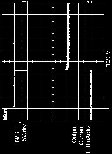
6 TYPICAL PERFORMANCE CHARACTERISTICS (V IN = 3.6 V, I OUT = 120 ma (6 LEDs at 20 ma), C IN = C OUT = C1 = C2 = 1 F, T AMB = 25 C unless otherwise specified.) OUTPUT VOLTAGE (V) x Mode Figure 14. Power Down Delay (1x Mode) OUTPUT CURRENT (ma) Figure 15. Foldback Current Limit Figure 16. Operating Waveforms in 1x Mode Figure 17. Switching Waveforms in 1.33x Mode Figure 18. Switching Waveforms in 1.5x Mode Figure 19. Switching Waveforms in 2x Mode 6
7 Table 5. PIN DESCRIPTION Pin # Name Function 1 LEDC2 LEDC2 cathode terminal 2 LEDC1 LEDC1 cathode terminal 3 LEDB2 LEDB2 cathode terminal 4 LEDB1 LEDB1 cathode terminal 5 LEDA2 LEDA2 cathode terminal 6 LEDA1 LEDA1 cathode terminal 7 VOUT Charge pump output, connect to LED anodes 8 VIN Charge pump input, connect to battery or supply 9 C1+ Bucket capacitor 1, positive terminal 10 C1 Bucket capacitor 1, negative terminal 11 C2+ Bucket capacitor 2, positive terminal 12 C2 Bucket capacitor 2, negative terminal 13/14 NC No connect 15 GND Ground reference 16 EN/SET Device enable (active high) and 1 wire control input TAB TAB Connect to GND on the PCB Pin Function VIN is the supply pin for the charge pump. A small 1 F ceramic bypass capacitor is required between the VIN pin and ground near the device. The operating input voltage range is from 2.5 V to 5.5 V. Whenever the input supply falls below the under voltage threshold (2 V) all the LED channels will be automatically disabled and the device register are reset to default values. EN/SET is the enable and one wire addressable control logic input for all LED channels. Guaranteed levels of logic high and logic low are set at 1.3 V and 0.4 V respectively. When EN/SET is initially taken high, the device becomes enabled and all LED currents remain at 0 ma. To place the device into zero current mode, the EN/SET pin must be held low for more than 1.5 ms. VOUT is the charge pump output that is connected to the LED anodes. A small 1 F ceramic bypass capacitor is required between the VOUT pin and ground near the device. GND is the ground reference for the charge pump. The pin must be connected to the ground plane on the PCB. C1+, C1 are connected to each side of the ceramic bucket capacitor C1. C2+, C2 are connected to each side of the ceramic bucket capacitor C2. LEDxx provide the internal regulated current for each of the LED cathodes. These pins enter high impedance zero current state whenever the device is placed in shutdown mode. TAB is the exposed pad underneath the package. For best thermal performance, the tab should be soldered to the PCB and connected to the ground plane. 7
8 Block Diagram C 1 C 1+ C 2 C 2+ V IN 1x mode (LDO) 1.33x, 1.5x, 2x Charge Pump V OUT EN/SET 0.8, 1.1 MHz Oscillator Mode Control LEDA1 LEDA2 LEDB1 LEDB2 100 k Serial Interface Reference Voltage LEDC1 LEDC2 Registers Current Setting DAC 6 Current Sink Regulators GND Figure 20. CAT3636 Functional Block Diagram Basic Operation At power up, the CAT3636 starts operating in 1x mode where the output will be approximately equal to the input supply voltage (less any internal voltage losses). If the output voltage is sufficient to regulate all LED currents, the device remains in 1x operating mode. If the input voltage is insufficient or falls to a level where the regulated currents cannot be maintained, the device automatically switches into 1.33x mode (after a fixed delay time of about 400 s). In 1.33x mode, the output voltage is approximately equal to 1.33 times the input supply voltage (less any internal voltage losses). If the input voltage is insufficient again or falls to a level where the regulated currents cannot be maintained, the device will automatically switch to the 1.5x boost mode (after a fixed delay time of about 400 s). In 1.5x mode, the output is approximately equal to 1.5 times the input supply voltage (less any internal voltage losses). If the input voltage fails more or is still insufficient to drive the LEDs, it will automatically switch again into 2x mode where the output is approximately equal to 2 times the input supply voltage (less any internal voltage losses). If the device detects a sufficient input voltage is present to drive all LED currents in 1x mode, it will change automatically back to 1x mode. This only applies for changing back to the 1x mode 8
9 LED Current Setting The current in each of the six LED channels is programmed through the 1 wire EN/SET digital control input. By pulsing this signal according to a specific protocol, a set of internal registers can be addressed and written into allowing to configure each bank of LEDs with the desired current. There are six registers: the first five are 4 bits long and the sixth is 1 bit long. The registers are programmed by first selecting the register address and then programming data into that register. An internal counter records the number of falling edges to identify the address and data. The address is serially programmed adhering to low and high duration time delays. One down pulse corresponds to register 1 being selected. Two down pulses correspond to register 2 being selected and so on up to register 6. T LO and T HI must be within 200 ns to 100 s. Anything below 200 ns may be ignored. Once the final rising edge of the address pointer is programmed, the user must wait 500 s to 1000 s before programming the first data pulse falling edge. If the falling edge of the data is not received within 1000 s, the device will revert back to waiting for an address. Data in a register is reset once it is selected by the address pointer. If a register is selected but no data is programmed, then the register value is reset back to its initial default value with all data bits to 0. Once the final rising edge of the data pulses is programmed, the user must wait 1.5 ms before programming another address. If programming fails or is interrupted, the user must wait T RESETDELAY 2 ms from the last rising edge before reprogramming can commence. Upon power up, the device automatically starts looking for an address. The device requires a minimum 10 s delay (T SETUP ) to ensure the initialization of the internal logic at power up. After this time delay, the device registers may be programmed adhering to the timing constraints shown in Figure 21. If no falling edge is detected within 100 s of power up, then the user must wait 2 ms before trying to program the device again. To power down the device and turn off all current sources, the EN/SET input should be kept low for a duration T OFF of 1.5 ms or more. The driver typically powers down with a delay of about 1 ms. All register data are lost. Figure 21. EN/SET One Wire Addressable Timing Diagram 9
10 Register Configuration and Programming Table 6. REGISTER ADDRESS AND DATA Register CAT3636 Address Pulses Description Bits DATA Pattern Bit 3 Bit 2 Bit 1 Bit 0 REG1 1 Bank Enable and IMODE 4 IMODE ENA ENB ENC REG2 2 Global Current Setting 4 REG3 3 Bank A Current Setting 4 REG4 4 Bank B Current Setting 4 REG5 5 Bank C Current Setting 4 See Table 8 for values REG6 6 Return Lockout 1 RTLKO Register REG1 allows to set the mode and select the pairs of LEDs to be turned on. A low LED current mode exists to allow for very low current operation under 4 ma per channel. If IMODE equals 1, the high current range is selected up to 32 ma. If IMODE is set to 0, all currents are divided by 8. Each bank of LEDs (A, B or C) can be turned on independently by setting the respective bit ENA, ENB, ENC to 1, as shown in Table 7. For example, to enable all 6 LEDs in low current mode, REG1 is programmed to 0111 binary (9 data pulses). Table 7. REG1 REGISTER SETTING Data Pulses REG1 Value (binary) IMODE Bank Enable ENA ENB ENC On On On On On On On On On On On On On On On On On On On On On On On On Register REG2 allows to set the same current for all 6 channels. REG3, REG4, REG5 allow to set the current respectively in banks A, B and C. The three banks can be programmed with independent current values. Table 8. REG2 5 CURRENT SETTING REGISTERS Data Pulses REGx Value (binary) LED Current IMODE = 0 LED Current IMODE = ma 2 ma ma 32 ma ma 30 ma ma 28 ma ma 26 ma ma 24 ma ma 22 ma ma 20 ma ma 18 ma ma 16 ma ma 14 ma ma 12 ma ma 10 ma ma 8 ma ma 6 ma ma 4 ma ma 2 ma REG6 contains the return lockout (RTLKO) bit. This stops the charge pump returning to 1x mode. One pulse sets it to 1. Two pulses or no pulses set RTLKO to 0. When RTLKO is set to 1, the charge pump cannot automatically return to 1x mode when in one of the charge pump modes. The device can however move from 1x to 1.33x to 1.5x to 2x if the input voltage is not sufficient to drive the programmed LED currents. REG6 also triggers a charge pump reset as soon as it is addressed. This forces the charge pump to start from 1x mode and reassess the correct mode it should be in to drive the LEDs most efficiently. If the input voltage has risen or the device has been reprogrammed to other LED values, it is recommended to trigger this reset allowing the charge pump to run in the most efficient mode. The CAT3636 enters a zero current shutdown mode if EN/SET is held low for 1.5 ms or more. All registers are reset back to zero when the device is placed in shutdown. 10


11 Programming Examples Programming 6 LEDs to 32 ma Programming 6 LEDs to 20 ma Programming 6 LEDs to 1 ma 11

12 Unused LED Channels For applications with only four or two LEDs, unused LED banks can be disabled via the enable register internally and left to float. For applications with 5 LEDs or less, unused LEDs can also be disabled by connecting the LED pin directly to VOUT, as shown on Figure 22. If LED pin voltage is within 1 V of VOUT, then the channel is switched off and a 200 A test current is placed in the channel to sense when the channel moves below VOUT 1 V. LED Selection LEDs with forward voltages (V F ) ranging from 1.3 V to 5.0 V may be used with the CAT3636. Selecting LEDs with lower V F is recommended in order to improve the efficiency by keeping the driver in 1x mode longer as the battery voltage decreases. For example, if a white LED with a V F of 3.3 V is selected over one with V F of 3.5 V, the CAT3636 will stay in 1x mode for lower supply voltage of 0.2 V. This helps improve the efficiency and extends battery life. External Components The driver requires two external 1 F ceramic capacitors for decoupling input, output, and for the charge pump. Both capacitors type X5R and X7R are recommended for the LED driver application. In all charge pump modes, the input current ripple is kept very low by design and an input bypass capacitor of 1 F is sufficient. In 1x mode, the device operates in linear mode and does not introduce switching noise back onto the supply. Figure 22. Five LED Application Protection Mode If an LED is disconnected, the output voltage V OUT automatically limits at about 5.5 V. This is to prevent the output pin from exceeding its absolute maximum rating. If the die temperature exceeds +150 C the driver will enter a thermal protection shutdown mode. When the device temperature drops by about 20 C the device will resume normal operation. Recommended Layout In charge pump mode, the driver switches internally at a high frequency. It is recommended to minimize trace length to all four capacitors. A ground plane should cover the area under the driver IC as well as the bypass capacitors. Short connection to ground on capacitors C IN and C OUT can be implemented with the use of multiple via. A copper area matching the TQFN exposed pad (TAB) must be connected to the ground plane underneath. The use of multiple via improves the package heat dissipation. Figure 23. Recommended Layout 12
13 PACKAGE DIMENSIONS TQFN16, 3x3 CASE 510AD ISSUE A D A e b L E E2 PIN#1 ID PIN#1 INDEX AREA A1 D2 TOP VIEW SIDE VIEW BOTTOM VIEW SYMBOL MIN NOM MAX A A A REF b D D E E e 0.50 BSC A A1 FRONT VIEW A3 L Notes: (1) All dimensions are in millimeters. (2) Complies with JEDEC MO All packages are RoHS compliant (Pb Free, Halogen Free). 6. The standard lead finish is NiPdAu. 7. For Matte Tin package option, please contact your nearest ON Semiconductor Sales office. ON Semiconductor and the are registered trademarks of Semiconductor Components Industries, LLC (SCILLC) or its subsidiaries in the United States and/or other countries. SCILLC owns the rights to a number of patents, trademarks, copyrights, trade secrets, and other intellectual property. A listing of SCILLC s product/patent coverage may be accessed at Marking.pdf. SCILLC reserves the right to make changes without further notice to any products herein. SCILLC makes no warranty, representation or guarantee regarding the suitability of its products for any particular purpose, nor does SCILLC assume any liability arising out of the application or use of any product or circuit, and specifically disclaims any and all liability, including without limitation special, consequential or incidental damages. Typical parameters which may be provided in SCILLC data sheets and/or specifications can and do vary in different applications and actual performance may vary over time. All operating parameters, including Typicals must be validated for each customer application by customer s technical experts. SCILLC does not convey any license under its patent rights nor the rights of others. SCILLC products are not designed, intended, or authorized for use as components in systems intended for surgical implant into the body, or other applications intended to support or sustain life, or for any other application in which the failure of the SCILLC product could create a situation where personal injury or death may occur. Should Buyer purchase or use SCILLC products for any such unintended or unauthorized application, Buyer shall indemnify and hold SCILLC and its officers, employees, subsidiaries, affiliates, and distributors harmless against all claims, costs, damages, and expenses, and reasonable attorney fees arising out of, directly or indirectly, any claim of personal injury or death associated with such unintended or unauthorized use, even if such claim alleges that SCILLC was negligent regarding the design or manufacture of the part. SCILLC is an Equal Opportunity/Affirmative Action Employer. This literature is subject to all applicable copyright laws and is not for resale in any manner. PUBLICATION ORDERING INFORMATION LITERATURE FULFILLMENT: Literature Distribution Center for ON Semiconductor P.O. Box 5163, Denver, Colorado USA Phone: or Toll Free USA/Canada Fax: or Toll Free USA/Canada orderlit@onsemi.com N. American Technical Support: Toll Free USA/Canada Europe, Middle East and Africa Technical Support: Phone: Japan Customer Focus Center Phone: ON Semiconductor Website: Order Literature: For additional information, please contact your local Sales Representative CAT3636/D
Programmable 300mA Camera Flash LED Driver
 Programmable 300mA Camera Flash LED Driver FEATURES Dual matched regulated LED channels 300mA output current (150mA per channel) 1-wire EZDim TM Programmable LED Current 32 accurate dimming levels Power
CAT3604V. 4-Channel LED Driver with Open/Short LED Detection
 CAT364V 4-Channel LED Driver with Open/Short LED Detection Description The CAT364V is a high efficiency fractional charge pump that can drive up to four LEDs with input supply voltages as low as 2.5 V.
LDS ma, Dual Output LED Flash/Lamp Driver FEATURES APPLICATION DESCRIPTION TYPICAL APPLICATION CIRCUIT
 200 ma, Dual Output LED Flash/Lamp Driver FEATURES o Multi-mode charge pump: 1-x, 1.5-x, 2-x o Ultra low dropout PowerLite Current Regulator* o Drives two high-current LEDs up to 96 ma each o 1-wire LED
1 A Constant-Current LED Driver with PWM Dimming
 1 A Constant-Current Driver with PWM Dimming FEATURES Accurate 1 A current sink Up to 25 V operation on pin Low dropout 500 mv at 1 A current set by external resistor High resolution PWM dimming via EN/PWM
CAT3200HU2. Low Noise Regulated Charge Pump DC-DC Converter
 CAT3HU Low Noise Regulated Charge Pump DC-DC Converter Description The CAT3HU is a switched capacitor boost converter that delivers a low noise, regulated output voltage. The CAT3HU gives a fixed regulated
LDS Channel Ultra Low Dropout LED Driver FEATURES APPLICATION DESCRIPTION TYPICAL APPLICATION CIRCUIT
 6-Channel Ultra Low Dropout LED Driver FEATURES o Ultra low dropout PowerLite Current Regulator o Multi-mode charge pump: 1x, 1.5x, 2x o Drives up to 6 LEDs at 32mA each o Factory preset current value
LDS Channel Ultra Low Dropout LED Driver FEATURES APPLICATION DESCRIPTION TYPICAL APPLICATION CIRCUIT
 6-Channel Ultra Low Dropout LED Driver FEATURES o Charge pump modes: 1-x, 1.33-x, 1.5-x, 2-x o Ultra low dropout PowerLite Current Regulator* o Drives up to 6 LEDs up to 32 ma each o Factory preset current
CAT5126. One time Digital 32 tap Potentiometer (POT)
") One time Digital 32 tap Potentiometer (POT) Description The CAT5126 is a digital POT. The wiper position is controlled with a simple 2-wire digital interface. This digital potentiometer is unique in that
One time Digital 32 tap Potentiometer (POT) Description The CAT5126 is a digital POT. The wiper position is controlled with a simple 2-wire digital interface. This digital potentiometer is unique in that
NTNS3164NZT5G. Small Signal MOSFET. 20 V, 361 ma, Single N Channel, SOT 883 (XDFN3) 1.0 x 0.6 x 0.4 mm Package
 1.0 x 0.6 x 0.4 mm Package") NTNS36NZ Small Signal MOSFET V, 36 ma, Single N Channel, SOT 883 (XDFN3). x.6 x. mm Package Features Single N Channel MOSFET Ultra Low Profile SOT 883 (XDFN3). x.6 x. mm for Extremely Thin Environments
NTNS36NZ Small Signal MOSFET V, 36 ma, Single N Channel, SOT 883 (XDFN3). x.6 x. mm Package Features Single N Channel MOSFET Ultra Low Profile SOT 883 (XDFN3). x.6 x. mm for Extremely Thin Environments
NTK3139P. Power MOSFET. 20 V, 780 ma, Single P Channel with ESD Protection, SOT 723
 NTK9P Power MOSFET V, 78 ma, Single P Channel with ESD Protection, SOT 7 Features P channel Switch with Low R DS(on) % Smaller Footprint and 8% Thinner than SC 89 Low Threshold Levels Allowing.5 V R DS(on)
NVLJD4007NZTBG. Small Signal MOSFET. 30 V, 245 ma, Dual, N Channel, Gate ESD Protection, 2x2 WDFN Package
 NVLJD7NZ Small Signal MOSFET V, 2 ma, Dual, N Channel, Gate ESD Protection, 2x2 WDFN Package Features Optimized Layout for Excellent High Speed Signal Integrity Low Gate Charge for Fast Switching Small
CAT4137. CMOS Boost Converter - White LED Driver
 CMOS Boost Converter - White LED Driver Description The CAT4137 is a DC/DC step-up converter that delivers a regulated output current. Operation at a constant switching frequency of 1 MHz allows the device
CAT884. Quad Voltage Supervisor
 Quad Voltage Supervisor Description The is a fourchannel power supply supervisory circuit with high accuracy reset thresholds and very low power consumption. The device features an activelow opendrain
CMPWR ma SmartOR Regulator with V AUX Switch
 50 ma SmartOR Regulator with Switch Product Description The ON Semiconductor s SmartOR is a low dropout regulator that delivers up to 50 ma of load current at a fixed 3.3 V output. An internal threshold
NSR0340V2T1/D. Schottky Barrier Diode 40 VOLT SCHOTTKY BARRIER DIODE
 Schottky Barrier Diode Schottky barrier diodes are optimized for very low forward voltage drop and low leakage current and are used in a wide range of dc dc converter, clamping and protection applications
CAX803, CAX809, CAX Pin Microprocessor Power Supply Supervisors
 3-Pin Microprocessor Power Supply Supervisors Description The CAX83, CAX89, and CAX81 are supervisory circuits that monitor power supplies in digital systems. The CAX83, CAX89, and CAX81 are direct replacements
NCP786L. Wide Input Voltage Range 5 ma Ultra-Low Iq, High PSRR Linear Regulator with Adjustable Output Voltage
 Wide Input Voltage Range 5 ma Ultra-Low Iq, High PSRR Linear Regulator with Adjustable Output Voltage The is high performance linear regulator, offering a very wide operating input voltage range of up
NTTFS3A08PZTWG. Power MOSFET 20 V, 15 A, Single P Channel, 8FL
 NTTFS3A8PZ Power MOSFET V, 5 A, Single P Channel, 8FL Features Ultra Low R DS(on) to Minimize Conduction Losses 8FL 3.3 x 3.3 x.8 mm for Space Saving and Excellent Thermal Conduction ESD Protection Level
PIN CONNECTIONS MAXIMUM RATINGS (T J = 25 C unless otherwise noted) SC 75 (3 Leads) Parameter Symbol Value Unit Drain to Source Voltage V DSS 30 V
 SC 75 (3 Leads) Parameter Symbol Value Unit Drain to Source Voltage V DSS 30 V") NTA7N, NVTA7N Small Signal MOSFET V, 4 ma, Single, N Channel, Gate ESD Protection, SC 7 Features Low Gate Charge for Fast Switching Small.6 x.6 mm Footprint ESD Protected Gate NV Prefix for Automotive
NTA7N, NVTA7N Small Signal MOSFET V, 4 ma, Single, N Channel, Gate ESD Protection, SC 7 Features Low Gate Charge for Fast Switching Small.6 x.6 mm Footprint ESD Protected Gate NV Prefix for Automotive
NTK3043N. Power MOSFET. 20 V, 285 ma, N Channel with ESD Protection, SOT 723
 NTKN Power MOSFET V, 8 ma, N Channel with ESD Protection, SOT 7 Features Enables High Density PCB Manufacturing % Smaller Footprint than SC 89 and 8% Thinner than SC 89 Low Voltage Drive Makes this Device
NCP5360A. Integrated Driver and MOSFET
 Integrated Driver and MOSFET The NCP5360A integrates a MOSFET driver, high-side MOSFET and low-side MOSFET into a 8mm x 8mm 56-pin QFN package. The driver and MOSFETs have been optimized for high-current
NCP ma, 10 V, Low Dropout Regulator
 15 ma, 1 V, Low Dropout Regulator The is a CMOS Linear voltage regulator with 15 ma output current capability. The device is capable of operating with input voltages up to 1 V, with high output voltage
NTHD4502NT1G. Power MOSFET. 30 V, 3.9 A, Dual N Channel ChipFET
 NTHDN Power MOSFET V,.9 A, Dual N Channel ChipFET Features Planar Technology Device Offers Low R DS(on) and Fast Switching Speed Leadless ChipFET Package has % Smaller Footprint than TSOP. Ideal Device
NTJD1155LT1G. Power MOSFET. 8 V, 1.3 A, High Side Load Switch with Level Shift, P Channel SC 88
 NTJDL Power MOSFET V,.3 A, High Side Load Switch with Level Shift, P Channel SC The NTJDL integrates a P and N Channel MOSFET in a single package. This device is particularly suited for portable electronic
NCP59302, NCV A, Very Low-Dropout (VLDO) Fast Transient Response Regulator series
 Fast Transient Response Regulator series") NCP5932, NCV5932 3. A, Very Low-Dropout (VLDO) Fast Transient Response Regulator series The NCP5932 is a high precision, very low dropout (VLDO), low ground current positive voltage regulator that is capable
NCP5932, NCV5932 3. A, Very Low-Dropout (VLDO) Fast Transient Response Regulator series The NCP5932 is a high precision, very low dropout (VLDO), low ground current positive voltage regulator that is capable
NCP304A. Voltage Detector Series
 Voltage Detector Series The NCP0A is a second generation ultralow current voltage detector. This device is specifically designed for use as a reset controller in portable microprocessor based systems where
NTJS4405N, NVJS4405N. Small Signal MOSFET. 25 V, 1.2 A, Single, N Channel, SC 88
 NTJSN, NVJSN Small Signal MOSFET V,. A, Single, N Channel, SC 88 Features Advance Planar Technology for Fast Switching, Low R DS(on) Higher Efficiency Extending Battery Life AEC Q Qualified and PPAP Capable
NDD60N360U1 35G. N-Channel Power MOSFET. 100% Avalanche Tested These Devices are Pb-Free, Halogen Free/BFR Free and are RoHS Compliant.
 NDDN3U N-Channel Power MOSFET V, 3 m Features % Avalanche Tested These Devices are Pb-Free, Halogen Free/BFR Free and are RoHS Compliant ABSOLUTE MAXIMUM RATINGS ( unless otherwise noted) V (BR)DSS R DS(ON)
NCP57302, NCV A, Very Low-Dropout (VLDO) Fast Transient Response Regulator
 Fast Transient Response Regulator") NCP5732, NC5732 3. A, ery Low-Dropout (LDO) Fast Transient Response Regulator The NCP5732 is a high precision, very low dropout (LDO), low minimum input voltage and low ground current positive voltage
NCP5732, NC5732 3. A, ery Low-Dropout (LDO) Fast Transient Response Regulator The NCP5732 is a high precision, very low dropout (LDO), low minimum input voltage and low ground current positive voltage
PZTA92T1. High Voltage Transistor. PNP Silicon SOT 223 PACKAGE PNP SILICON HIGH VOLTAGE TRANSISTOR SURFACE MOUNT
 High Voltage Transistor PNP Silicon Features These Devices are Pb Free, Halogen Free/BFR Free and are RoHS Compliant MAXIMUM RATINGS (T C = 25 C unless otherwise noted) Rating Symbol Value Unit Collector-Emitter
NTS4172NT1G. Power MOSFET. 30 V, 1.7 A, Single N Channel, SC 70. Low On Resistance Low Gate Threshold Voltage Halide Free This is a Pb Free Device
 Power MOSFET V,.7 A, Single N Channel, SC 7 Features Low On Resistance Low Gate Threshold Voltage Halide Free This is a Pb Free Device V (BR)DSS R DS(on) MAX I D MAX Applications Low Side Load Switch DC
NCP331. Soft-Start Controlled Load Switch with Auto Discharge
 Soft-Start Controlled Load Switch with Auto Discharge The NCP331 is a low Ron N channel MOSFET controlled by a soft start sequence of 2 ms for mobile applications. The very low R DS(on) allows system supplying
PCS2I2309NZ. 3.3 V 1:9 Clock Buffer
 . V 1:9 Clock Buffer Functional Description PCS2I209NZ is a low cost high speed buffer designed to accept one clock input and distribute up to nine clocks in mobile PC systems and desktop PC systems. The
NCP5504, NCV ma Dual Output Low Dropout Linear Regulator
 25 ma Dual Output Low Dropout Linear Regulator The NCP554/NCV554 are dual output low dropout linear regulators with 2.% accuracy over the operating temperature range. They feature a fixed output voltage
MUN5216DW1, NSBC143TDXV6. Dual NPN Bias Resistor Transistors R1 = 4.7 k, R2 = k. NPN Transistors with Monolithic Bias Resistor Network
 MUN526DW, NSBC43TDXV6 Dual NPN Bias Resistor Transistors R = 4.7 k, R2 = k NPN Transistors with Monolithic Bias Resistor Network This series of digital transistors is designed to replace a single device
MBD110DWT1G MBD330DWT1G. Dual Schottky Barrier Diodes
 , Dual Schottky Barrier Diodes Application circuit designs are moving toward the consolidation of device count and into smaller packages. The new SOT363 package is a solution which simplifies circuit design,
LM339S, LM2901S. Single Supply Quad Comparators
 LM339S, LM290S Single Supply Quad Comparators These comparators are designed for use in level detection, low level sensing and memory applications in consumer and industrial electronic applications. Features
NTNUS3171PZ. Small Signal MOSFET. 20 V, 200 ma, Single P Channel, 1.0 x 0.6 mm SOT 1123 Package
 NTNUS7PZ Small Signal MOSFET V, ma, Single P Channel,. x.6 mm SOT Package Features Single P Channel MOSFET Offers a Low R DS(on) Solution in the Ultra Small. x.6 mm Package. V Gate Voltage Rating Ultra
CAT853, CAT859, CAT863, CAT869 3-Pin Microprocessor Power Supply Supervisors
 CAT853, CAT859, CAT863, CAT869 3-Pin Microprocessor Power Supply Supervisors Description The CAT853, CAT863, CAT859, and CAT869 are supervisory circuits that monitor power supplies in digital systems.
NVD5117PLT4G. Power MOSFET 60 V, 16 m, 61 A, Single P Channel
 Power MOSFET 6 V, 16 m, 61 A, Single P Channel Features Low R DS(on) to Minimize Conduction Losses High Current Capability Avalanche Energy Specified AEC Q11 Qualified These Devices are Pb Free, Halogen
NTMS5835NL. Power MOSFET 40 V, 12 A, 10 m
 Power MOSFET V, 2 A, m Features Low R DS(on) Low Capacitance Optimized Gate Charge These Devices are Pb Free, Halogen Free/BFR Free and are RoHS Compliant MAXIMUM RATINGS ( unless otherwise stated) Parameter
NTLUS3A90PZ. Power MOSFET 20 V, 5.0 A, Cool Single P Channel, ESD, 1.6x1.6x0.55 mm UDFN Package
 NTLUS3A9PZ Power MOSFET V, 5. A, Cool Single P Channel, ESD,.x.x.55 mm UDFN Package Features UDFN Package with Exposed Drain Pads for Excellent Thermal Conduction Low Profile UDFN.x.x.55 mm for Board Space
NTA4001N, NVA4001N. Small Signal MOSFET. 20 V, 238 ma, Single, N Channel, Gate ESD Protection, SC 75
 Small Signal MOSFET V, 8 ma, Single, N Channel, Gate ESD Protection, SC 75 Features Low Gate Charge for Fast Switching Small.6 x.6 mm Footprint ESD Protected Gate AEC Q Qualified and PPAP Capable NVA4N
NTD5867NL. N-Channel Power MOSFET 60 V, 20 A, 39 m
 N-Channel Power MOSFET 6 V, A, 39 m Features Low R DS(on) High Current Capability % Avalanche Tested These Devices are Pb Free, Halogen Free/BFR Free and are RoHS Compliant MAXIMUM RATINGS ( unless otherwise
NTMS5838NL. Power MOSFET 40 V, 7.5 A, 20 m
 Power MOSFET V, 7.5 A, 2 m Features Low R DS(on) Low Capacitance Optimized Gate Charge These Devices are Pb Free, Halogen Free/BFR Free and are RoHS Compliant MAXIMUM RATINGS ( unless otherwise stated)
 Distributed by: www.jameco.com 1-800-831-44 The content and copyrights of the attached material are the property of its owner. Transient Voltage Suppressors Micro Packaged Diodes for ESD Protection The
SS13FL, SS14FL. Surface Mount Schottky Barrier Rectifier
 SS13FL, SS14FL Surface Mount Schottky Barrier Rectifier Features Ultra Thin Profile Maximum Height of 1.08 mm UL Flammability 94V 0 Classification MSL 1 Green Mold Compound These Devices are Pb Free, Halogen
LDS8710. High Efficiency 10 LED Driver With No External Schottky FEATURES APPLICATION DESCRIPTION TYPICAL APPLICATION CIRCUIT
 High Efficiency 10 LED Driver With No External Schottky FEATURES High efficiency boost converter with the input voltage range from 2.7 to 5.5 V No external Schottky Required (Internal synchronous rectifier*)
NTD5865NL. N-Channel Power MOSFET 60 V, 46 A, 16 m
 N-Channel Power MOSFET 6 V, 6 A, 6 m Features Low Gate Charge Fast Switching High Current Capability % Avalanche Tested These Devices are Pb Free, Halogen Free and are RoHS Compliant MAXIMUM RATINGS (
NVD5865NL. Power MOSFET 60 V, 46 A, 16 m, Single N Channel
 Power MOSFET 6 V, 6 A, 16 m, Single N Channel Features Low R DS(on) to Minimize Conduction Losses High Current Capability Avalanche Energy Specified AEC Q1 Qualified These Devices are Pb Free, Halogen
P2I2305NZ. 3.3V 1:5 Clock Buffer
 3.3V :5 Clock Buffer Functional Description P2I2305NZ is a low cost high speed buffer designed to accept one clock input and distribute up to five clocks in mobile PC systems and desktop PC systems. The
NTTFS5116PLTWG. Power MOSFET 60 V, 20 A, 52 m. Low R DS(on) Fast Switching These Devices are Pb Free and are RoHS Compliant
 Fast Switching These Devices are Pb Free and are RoHS Compliant") Power MOSFET 6 V, 2 A, 52 m Features Low R DS(on) Fast Switching These Devices are Pb Free and are RoHS Compliant Applications Load Switches DC Motor Control DC DC Conversion MAXIMUM RATINGS ( unless otherwise
Power MOSFET 6 V, 2 A, 52 m Features Low R DS(on) Fast Switching These Devices are Pb Free and are RoHS Compliant Applications Load Switches DC Motor Control DC DC Conversion MAXIMUM RATINGS ( unless otherwise
NTA4153N, NTE4153N, NVA4153N, NVE4153N. Small Signal MOSFET. 20 V, 915 ma, Single N Channel with ESD Protection, SC 75 and SC 89
 NTA45N, NTE45N, NVA45N, NVE45N Small Signal MOSFET V, 95 ma, Single N Channel with ESD Protection, SC 75 and SC 89 Features Low R DS(on) Improving System Efficiency Low Threshold Voltage,.5 V Rated ESD
NCP694. 1A CMOS Low-Dropout Voltage Regulator
 A CMOS Low-Dropout Voltage Regulator The NCP694 series of fixed output super low dropout linear regulators are designed for portable battery powered applications with high output current requirement up
NSVEMD4DXV6T5G. Dual Bias Resistor Transistors. NPN and PNP Silicon Surface Mount Transistors with Monolithic Bias Resistor Network
 Dual Bias Resistor Transistors NPN and PNP Silicon Surface Mount Transistors with Monolithic Bias Resistor Network The BRT (Bias Resistor Transistor) contains a single transistor with a monolithic bias
NCP A Low Dropout Linear Regulator
 1.5 A Low Dropout Linear Regulator The NCP566 low dropout linear regulator will provide 1.5 A at a fixed output voltage. The fast loop response and low dropout voltage make this regulator ideal for applications
NTLUD3A260PZ. Power MOSFET 20 V, 2.1 A, Cool Dual P Channel, ESD, 1.6x1.6x0.55 mm UDFN Package
 NTLUDAPZ Power MOSFET V,. A, Cool Dual P Channel, ESD,.x.x. mm UDFN Package Features UDFN Package with Exposed Drain Pads for Excellent Thermal Conduction Low Profile UDFN.x.x. mm for Board Space Saving
BAT54CLT3G SBAT54CLT1G. Dual Common Cathode Schottky Barrier Diodes 30 VOLT DUAL COMMON CATHODE SCHOTTKY BARRIER DIODES
 BAT54CLTG, SBAT54CLTG Dual Common Cathode Schottky Barrier Diodes These Schottky barrier diodes are designed for high speed switching applications, circuit protection, and voltage clamping. Extremely low
NVTFS4C13N. Power MOSFET. 30 V, 9.4 m, 40 A, Single N Channel, 8FL Features
 NVTFS4C3N Power MOSFET 3 V, 9.4 m, 4 A, Single N Channel, 8FL Features Low R DS(on) to Minimize Conduction Losses Low Capacitance to Minimize Driver Losses Optimized Gate Charge to Minimize Switching Losses
7WB Bit Bus Switch. The 7WB3126 is an advanced high speed low power 2 bit bus switch in ultra small footprints.
 2-Bit Bus Switch The WB326 is an advanced high speed low power 2 bit bus switch in ultra small footprints. Features High Speed: t PD = 0.25 ns (Max) @ V CC = 4.5 V 3 Switch Connection Between 2 Ports Power
NTTFS5820NLTWG. Power MOSFET. 60 V, 37 A, 11.5 m. Low R DS(on) Low Capacitance Optimized Gate Charge These Devices are Pb Free and are RoHS Compliant
 Low Capacitance Optimized Gate Charge These Devices are Pb Free and are RoHS Compliant") NTTFS582NL Power MOSFET 6 V, 37 A,.5 m Features Low R DS(on) Low Capacitance Optimized Gate Charge These Devices are Pb Free and are RoHS Compliant MAXIMUM RATINGS ( unless otherwise stated) Parameter
NTTFS582NL Power MOSFET 6 V, 37 A,.5 m Features Low R DS(on) Low Capacitance Optimized Gate Charge These Devices are Pb Free and are RoHS Compliant MAXIMUM RATINGS ( unless otherwise stated) Parameter
NTGS3441BT1G. Power MOSFET. -20 V, -3.5 A, Single P-Channel, TSOP-6. Low R DS(on) in TSOP-6 Package 2.5 V Gate Rating This is a Pb-Free Device
 in TSOP-6 Package 2.5 V Gate Rating This is a Pb-Free Device") Power MOSFET - V, -. A, Single P-Channel, TSOP- Features Low R DS(on) in TSOP- Package. V Gate Rating This is a Pb-Free Device Applications Battery Switch and Load Management Applications in Portable Equipment
Power MOSFET - V, -. A, Single P-Channel, TSOP- Features Low R DS(on) in TSOP- Package. V Gate Rating This is a Pb-Free Device Applications Battery Switch and Load Management Applications in Portable Equipment
NTS4173PT1G. Power MOSFET. 30 V, 1.3 A, Single P Channel, SC 70
 NTS17P Power MOSFET V, 1. A, Single P Channel, SC 7 Features V BV ds, Low R DS(on) in SC 7 Package Low Threshold Voltage Fast Switching Speed This is a Halide Free Device This is a Pb Free Device Applications
NTR4101P, NTRV4101P. Trench Power MOSFET 20 V, Single P Channel, SOT 23
 NTRP, NTRVP Trench Power MOSFET V, Single P Channel, SOT Features Leading V Trench for Low R DS(on). V Rated for Low Voltage Gate Drive SOT Surface Mount for Small Footprint NTRV Prefix for Automotive
S1AFL - S1MFL. Surface General-Purpose Rectifier
 SAFL - SMFL Surface General-Purpose Rectifier Features Ultra Thin Profile Maximum Height of.08 mm UL Flammability 94V 0 Classification MSL Green Mold Compound These Devices are Pb Free, Halogen Free Free
NLHV18T Channel Level Shifter
 18-Channel Level Shifter The NLHV18T3244 is an 18 channel level translator designed for high voltage level shifting applications such as displays. The 18 channels are divided into twelve and two three
MBR130LSFT1G. Surface Mount Schottky Power Rectifier. Plastic SOD 123 Package SCHOTTKY BARRIER RECTIFIER 1.0 AMPERES, 30 VOLTS
 MBR3LSFTG Surface Mount Schottky Power Rectifier Plastic SOD 23 Package This device uses the Schottky Barrier principle with a large area metal to silicon power diode. Ideally suited for low voltage, high
P3P85R01A. 3.3V, 75 MHz to 200 MHz LVCMOS TIMING SAFE Peak EMI Reduction Device
 3.3V, 75 MHz to 200 MHz LVCMOS TIMING SAFE Peak EMI Reduction Device Functional Description P3P85R0A is a versatile, 3.3 V, LVCMOS, wide frequency range, TIMING SAFE Peak EMI reduction device. TIMING SAFE
MMBTA06W, SMMBTA06W, Driver Transistor. NPN Silicon. Moisture Sensitivity Level: 1 ESD Rating: Human Body Model 4 kv ESD Rating: Machine Model 400 V
 Driver Transistor NPN Silicon Moisture Sensitivity Level: 1 ESD Rating: Human Body Model 4 kv ESD Rating: Machine Model 400 V Features S Prefix for Automotive and Other Applications Requiring Unique Site
MUN5311DW1T1G Series.
 MUNDWTG Series Preferred Devices Dual Bias Resistor Transistors NPN and PNP Silicon Surface Mount Transistors with Monolithic Bias Resistor Network The Bias Resistor Transistor (BRT) contains a single
NTR4502P, NVTR4502P. Power MOSFET. 30 V, 1.95 A, Single, P Channel, SOT 23
 NTRP, NVTRP Power MOSFET V,.9 A, Single, P Channel, SOT Features Leading Planar Technology for Low Gate Charge / Fast Switching Low R DS(ON) for Low Conduction Losses SOT Surface Mount for Small Footprint
NUS2045MN, NUS3045MN. Overvoltage Protection IC with Integrated MOSFET
 , Overvoltage Protection IC with Integrated MOSFET These devices represent a new level of safety and integration by combining the NCP34 overvoltage protection circuit (OVP) with a 2 V P channel power MOSFET
NDF10N62Z. N-Channel Power MOSFET
 NDFNZ N-Channel Power MOSFET V,.7 Features Low ON Resistance Low Gate Charge ESD Diode Protected Gate % Avalanche Tested These Devices are Pb Free, Halogen Free/BFR Free and are RoHS Compliant V DSS R
NTD5805N, NVD5805N. Power MOSFET 40 V, 51 A, Single N Channel, DPAK
 NTD585N, NVD585N Power MOSFET V, 5 A, Single N Channel, Features Low R DS(on) High Current Capability Avalanche Energy Specified NVD Prefix for Automotive and Other Applications Requiring Unique Site and
NTGD4167C. Power MOSFET Complementary, 30 V, +2.9/ 2.2 A, TSOP 6 Dual
 Power MOSFET Complementary, 3 V, +.9/. A, TSOP 6 Dual Features Complementary N Channel and P Channel MOSFET Small Size (3 x 3 mm) Dual TSOP 6 Package Leading Edge Trench Technology for Low On Resistance
MMSD301T1G SMMSD301T1G, MMSD701T1G SMMSD701T1G, SOD-123 Schottky Barrier Diodes
 MMSD3TG, SMMSD3TG, MMSD7TG, SMMSD7TG, SOD-3 Schottky Barrier Diodes The MMSD3T, and MMSD7T devices are spinoffs of our popular MMBD3LT, and MMBD7LT SOT3 devices. They are designed for highefficiency UHF
MBRM110LT3G NRVBM110LT1G NRVBM110LT3G. Surface Mount Schottky Power Rectifier. POWERMITE Power Surface Mount Package
 MBRM11LT1G, NRVBM11LT1G, NRVBM11LT3G Surface Mount Schottky Power Rectifier Power Surface Mount Package The Schottky employs the Schottky Barrier principle with a barrier metal and epitaxial construction
MBRA320T3G Surface Mount Schottky Power Rectifier
 Surface Mount Schottky Power Rectifier Power Surface Mount Package Employing the Schottky Barrier principle in a large area metal to silicon power diode. State of the art geometry features epitaxial construction
MMSZ5221BT1 Series. Zener Voltage Regulators. 500 mw SOD 123 Surface Mount
 MMSZ5BT Series Preferred Device Zener Voltage Regulators 5 mw SOD 3 Surface Mount Three complete series of Zener diodes are offered in the convenient, surface mount plastic SOD 3 package. These devices
AND8285/D. NCP1521B Adjustable Output Voltage Step Down Converter Simulation Procedure SIMULATION NOTE
 NCP1521B Adjustable Output Voltage Step Down Converter Simulation Procedure Prepared by: Bertrand Renaud On Semiconductor SIMULATION NOTE Overview The NCP1521B step down PWM DC DC converter is optimized
NSQA6V8AW5T2 Series Transient Voltage Suppressor
 Transient Voltage Suppressor ESD Protection Diode with Low Clamping Voltage This integrated transient voltage suppressor device (TVS) is designed for applications requiring transient overvoltage protection.
NSS1C201L, NSV1C201L. 100 V, 3.0 A, Low V CE(sat) NPN Transistor. 100 VOLTS, 3.0 AMPS NPN LOW V CE(sat) TRANSISTOR
 NPN Transistor. 100 VOLTS, 3.0 AMPS NPN LOW V CE(sat) TRANSISTOR") NSSCL, NSVCL V,. A, Low V CE(sat) NPN Transistor ON Semiconductor s e PowerEdge family of low V CE(sat) transistors are miniature surface mount devices featuring ultra low saturation voltage (V CE(sat)
NSSCL, NSVCL V,. A, Low V CE(sat) NPN Transistor ON Semiconductor s e PowerEdge family of low V CE(sat) transistors are miniature surface mount devices featuring ultra low saturation voltage (V CE(sat)
NTMFS5C604NL. Power MOSFET. 60 V, 1.2 m, 276 A, Single N Channel
 NTMFSC64NL Power MOSFET 6 V,. m, 76 A, Single N Channel Features Small Footprint (x6 mm) for Compact esign Low R S(on) to Minimize Conduction Losses Low Q G and Capacitance to Minimize river Losses These
MUR405, MUR410, MUR415, MUR420, MUR440, MUR460. SWITCHMODE Power Rectifiers ULTRAFAST RECTIFIERS 4.0 AMPERES, VOLTS
 MUR45, MUR4, MUR415, MUR42, MUR44, MUR46 SWITCHMODE Power Rectifiers These state of the art devices are a series designed for use in switching power supplies, inverters and as free wheeling diodes. Features
FPF2498. Adjustable OVP with 28 V Input OVT Load Switch. Cellular Phones, Smart Phones Tablets. FPF2498 Evaluation Board
 Adjustable OVP with 28 V Input OVT Load Switch Description The advanced load management switch targets applications requiring a highly integrated solution. It disconnects loads powered from the DC power
ESD7381MUT5G Transient Voltage Suppressors Micro Packaged Diodes for ESD Protection
 Transient Voltage Suppressors Micro Packaged Diodes for SD Protection The SD738 is designed to protect voltage sensitive components that require ultra low capacitance from SD and transient voltage events.
MMBFU310LT1G. JFET Transistor. N Channel. These Devices are Pb Free, Halogen Free/BFR Free and are RoHS Compliant. Features.
 MMBFULT1G JFET Transistor N Channel Features These Devices are Pb Free, Halogen Free/BFR Free and are RoHS Compliant 2 SOURCE MAXIMUM RATINGS Rating Symbol Value Unit Drain Source Voltage V DS 25 Vdc Gate
NVC6S5A444NLZ. Power MOSFET. 60 V, 78 m, 4.5 A, N Channel
 Power MOSFET 6 V, 78 m,.5 A, N Channel Automotive Power MOSFET designed to minimize gate charge and low on resistance. AEC Q qualified MOSFET and PPAP capable suitable for automotive applications. Features.5
MJD44H11 (NPN) MJD45H11 (PNP)
 MJD45H11 (PNP)") MJDH (NPN) MJD5H (PNP) Preferred Device Complementary Power Transistors For Surface Mount Applications Designed for general purpose power and switching such as output or driver stages in applications such
MJDH (NPN) MJD5H (PNP) Preferred Device Complementary Power Transistors For Surface Mount Applications Designed for general purpose power and switching such as output or driver stages in applications such
NTMFS4936NCT3G. NTMFS4936NC Power MOSFET 30 V, 79 A, Single N Channel, SO 8 FL
 NTMFS4936N, NTMFS4936NC Power MOSFET 3 V, 79 A, Single N Channel, Features Low R S(on), Low Capacitance and Optimized Gate Charge to Minimize Conduction, river and Switching Losses Next Generation Enhanced
NTS2101P. Power MOSFET. 8.0 V, 1.4 A, Single P Channel, SC 70
 NTS11P Power MOSFET 8. V, 1.4 A, Single P Channel, SC 7 Features Leading Trench Technology for Low R DS(on) Extending Battery Life 1.8 V Rated for Low Voltage Gate Drive SC 7 Surface Mount for Small Footprint
MUN5332DW1, NSBC143EPDXV6, NSBC143EPDP6. Complementary Bias Resistor Transistors R1 = 4.7 k, R2 = 4.7 k
 MUN5DW, NSBCEPDXV6, NSBCEPDP6 Complementary Bias Resistor Transistors R =.7 k, R =.7 k NPN and PNP Transistors with Monolithic Bias Resistor Network () PIN CONNECTIONS () () This series of digital transistors
NCP ma, Wide Input Voltage Range, Low Dropout Regulator
 5 ma, Wide Input Voltage Range, Low Dropout Regulator The NCP4623 is a CMOS Linear Voltage Regulator designed for wide input voltage range. The maximum operating input voltage is up to 24 V with a minimum
MURS320T3G, SURS8320T3G, MURS340T3G, SURS8340T3G, MURS360T3G, SURS8360T3G. Surface Mount Ultrafast Power Rectifiers
 MURS32T3G, SURS832T3G, MURS34T3G, SURS834T3G, MURS36T3G, Surface Mount Ultrafast Power Rectifiers This series employs the state of the art epitaxial construction with oxide passivation and metal overlay
MRA4003T3G Series, NRVA4003T3G Series. Surface Mount Standard Recovery Power Rectifier. SMA Power Surface Mount Package
 MRA43T3G Series, NRVA43T3G Series Surface Mount Standard Recovery Power Rectifier Power Surface Mount Package Features construction with glass passivation. Ideally suited for surface mounted automotive
NTLUF4189NZ Power MOSFET and Schottky Diode
 NTLUF89NZ Power MOSFET and Schottky Diode V, N Channel with. A Schottky Barrier Diode,. x. x. mm Cool Package Features Low Qg and Capacitance to Minimize Switching Losses Low Profile UDFN.x. mm for Board
NCP A, Low Dropout Linear Regulator with Enhanced ESD Protection
 3.0 A, Low Dropout Linear Regulator with Enhanced ESD Protection The NCP5667 is a high performance, low dropout linear regulator designed for high power applications that require up to 3.0 A current. A
NCP170. Ultra Low I Q 150 ma CMOS LDO Regulator
 NCP17 Ultra Low I Q 15 ma CMOS LDO Regulator The NCP17 series of CMOS low dropout regulators are designed specifically for portable battery-powered applications which require ultra-low quiescent current.
NTMS4801NR2G. Power MOSFET 30 V, 12 A, N Channel, SO 8
 NTMSN Power MOSFET 3 V, A, N Channel, SO Features Low R DS(on) to Minimize Conduction Losses Low Capacitance to Minimize Driver Losses Optimized Gate Charge to Minimize Switching Losses This is a Pb Free
MURS120T3G Series, SURS8120T3G Series. Surface Mount Ultrafast Power Rectifiers
 MURS12T3G Series, SURS812T3G Series Surface Mount Ultrafast Power Rectifiers MURS5T3G, MURS1T3G, MURS115T3G, MURS12T3G, MURS14T3G, MURS16T3G, SURS85T3G, SURS81T3G, SURS8115T3G, SURS812T3G, SURS814T3G,