CHAPTER 9 FEEDBACK. NTUEE Electronics L.H. Lu 9-1
|
|
|
- Rosamond Cox
- 6 years ago
- Views:
Transcription
1 CHAPTER 9 FEEDBACK Chapter Outline 9.1 The General Feedback Structure 9.2 Some Properties of Negative Feedback 9.3 The Four Basic Feedback Topologies 9.4 The Feedback Voltage Amplifier (Series-Shunt) 9.5 The Feedback Transconductance Amplifier (Series-Series) 9.6 The Feedback Transresistance Amplifier (Shunt-Shunt) 9.7 The Feedback Current Amplifier (Shunt-Series) 9.9 Determining the Loop Gain 9.10 The Stability Problem 9.11 Effect of Feedback on the Amplifier Poles 9.12 Stability Study Using Bode Plots 9.13 Frequency Compensation NTUEE Electronics L.H. Lu 9-1
: Negative feedback: The feedback signal x f is subtracted from the source signal x s Negative feedback reduces the signal that appears at the input of the basic amplifier")
2 9.1 The General Feedback Structure Feedback amplifier Signal-flow diagram of a feedback amplifier Open-loop gain: A Feedback factor: Loop gain: A Amount of feedback: 1 + A Gain of the feedback amplifier (closed-loop gain): Negative feedback: The feedback signal x f is subtracted from the source signal x s Negative feedback reduces the signal that appears at the input of the basic amplifier The gain of the feedback amplifier A f is smaller than open-loop gain A by a factor of (1+A ) The loop gain A is typically large (A >>1): The gain of the feedback amplifier (closed-loop gain) A f 1/ The closed-loop gain is almost entirely determined by the feedback network better accuracy of A f x f = x s (A )/(1+A ) x s error signal x i = x s x f NTUEE Electronics L.H. Lu 9-2
 Find the condition under which the closed-loop gain A f is almost entirely determined by the feedback network.")
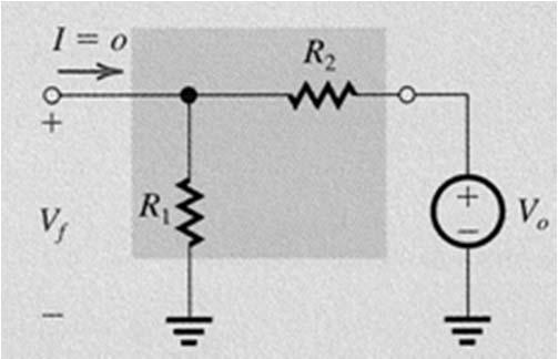
3 Example The feedback amplifier is based on an opamp with infinite input resistance and zero output resistance (a) Find an expression for the feedback factor. (b) Find the condition under which the closed-loop gain A f is almost entirely determined by the feedback network. (c) If the open-loop gain A = V/V, find R 2 /R 1 to obtain a closed-loop gain A f of 10 V/V. (d) What is the amount of feedback in decibel? (e) If V s = 1 V, find V o, V f and V i. (f) If A decreases by 20%, what is the corresponding decrease in A f? NTUEE Electronics L.H. Lu 9-3
4 9.2 Some Properties of Negative Feedback Gain desensitivity The negative reduces the change in the closed-loop gain due to open-loop gain variation Desensitivity factor: 1+ A Bandwidth extension High-frequency response of a single-pole amplifier: Low-frequency response of an amplifier with a dominant low-frequency pole: Negative feedback: Reduces the gain by a factor of (1+A M ) Extends the bandwidth by a factor of (1+A M ) NTUEE Electronics L.H. Lu 9-4
5 Interference reduction The signal-to-noise ratio: The amplifier suffers from interference introduced at the input of the amplifier Signal-to-noise ratio: S/I = V s /V n Enhancement of the signal-to-noise ratio: Precede the original amplifier A 1 by a clean amplifier A 2 Use negative feedback to keep the overall gain constant NTUEE Electronics L.H. Lu 9-5
6 Reduction in nonlinear distortion The amplifier transfer characteristic is linearized through the application of negative feedback = 0.01 A changes from 1000 to 100 NTUEE Electronics L.H. Lu 9-6
7 9.3 The Four Basic Feedback Topologies Voltage amplifiers The most suitable feedback topologies is voltage-mixing and voltage-sampling one Known as series-shunt feedback Example: NTUEE Electronics L.H. Lu 9-7
8 Current amplifiers The most suitable feedback topologies is current-mixing and current-sampling one Known as shunt-series feedback Example: NTUEE Electronics L.H. Lu 9-8
9 Transconductance amplifiers The most suitable feedback topologies is voltage-mixing and current-sampling one Known as series-series feedback Example: NTUEE Electronics L.H. Lu 9-9

10 Transresistance amplifiers The most suitable feedback topologies is current-mixing and voltage-sampling one Known as shunt-shunt feedback Example: NTUEE Electronics L.H. Lu 9-10


11 9.4 The Feedback Voltage Amplifier (Series-Shunt) Ideal case Input resistance of the feedback amplifier Output resistance of the feedback amplifier Voltage gain of the feedback amplifier NTUEE Electronics L.H. Lu 9-11


12 The practical case NTUEE Electronics L.H. Lu 9-12

13 NTUEE Electronics L.H. Lu 9-13

14 Analysis techniques NTUEE Electronics L.H. Lu 9-14

15 Example NTUEE Electronics L.H. Lu 9-15


16 Example NTUEE Electronics L.H. Lu 9-16
 Ideal case Input resistance of the")

17 9.5 The Feedback Transconductance Amplifier (Series-Series) Ideal case Input resistance of the feedback amplifier Output resistance of the feedback amplifier Voltage gain of the feedback amplifier NTUEE Electronics L.H. Lu 9-17


18 The practical case NTUEE Electronics L.H. Lu 9-18
19 Analysis techniques NTUEE Electronics L.H. Lu 9-19
 Ideal case Input resistance of the")

20 9.6 The Feedback Transresistance Amplifier (Shunt-Shunt) Ideal case Input resistance of the feedback amplifier Output resistance of the feedback amplifier Voltage gain of the feedback amplifier NTUEE Electronics L.H. Lu 9-20


21 9.7 The Feedback Current Amplifier (Shunt-Series) Ideal case Input resistance of the feedback amplifier Output resistance of the feedback amplifier Voltage gain of the feedback amplifier NTUEE Electronics L.H. Lu 9-21
22 9.9 Determining the Loop Gain An Alternative Approach for Finding Loop Gain Open-loop analysis with equivalent loading: Remove the external source Break the loop with equivalent loading Provide test signal V t Loop gain: Equivalent method for determining loop gain: Usually convenient to employ in simulation Remove the external source Break the loop Provide test signal V t Find the open-circuit voltage transfer function T oc Find the short-circuit current transfer function T sc Loop gain: The value of loop gain determined using the method discussed here may differ somewhat from the value determined by the approach studied in the previous session, but the difference is usually limited to a few percent. NTUEE Electronics L.H. Lu 9-22
23 Example NTUEE Electronics L.H. Lu 9-23
24 Characteristic Equation The gain of a feedback amplifier can be expressed as a transfer function (function of s) by taking the frequency-dependent properties into consideration. The denominator determines the poles of the system and the numerator defines the zeros. From the study of circuit theory that the poles of a circuit are independent of the external excitation. The poles or the natural modes can be determined by setting the external excitation to zero. The characteristic equation and the poles are completely determined by the loop gain. A given feedback loop may be used to general a number of circuits having the same poles but different transmission zeros. the closed-loop gain and the transmission zeros depend on how and where the input signal is injected into the loop. NTUEE Electronics L.H. Lu 9-24
25 9.10 The Stability Problem Transfer function of the feedback amplifier Transfer functions: Open-loop transfer function: A(s) Feedback transfer function: (s) Closed-loop transfer function: A f (s) For physical frequencies s = j Loop gain: Stability of the closed-loop transfer function: For loop gain smaller than unity at 180 : Becomes positive feedback Closed-loop gain becomes larger than open-loop gain The feedback amplifier is still stable For loop gain equal to unity at 180 : The amplifier will have an output for zero input (oscillation) For loop gain larger than unity at 180 : Oscillation with a growing amplitude at the output NTUEE Electronics L.H. Lu 9-25
26 The Nyquist plot A plot used to evaluate the stability of a feedback amplifier Plot the loop gain versus frequency on the complex plane Stability: The plot does not encircle the point (-1, 0) NTUEE Electronics L.H. Lu 9-26
27 9.11 Effect of Feedback on the Amplifier Poles Stability and pole location Consider an amplifier with a pole pair at The transient response contains the terms of the form NTUEE Electronics L.H. Lu 9-27
28 Poles of the feedback amplifier Characteristic equation: 1+A(s) (s) = 0 The feedback amplifier poles are obtained by solving the characteristic equation Amplifier with single-pole response The feedback amplifier is still a single-pole system The pole moves away from origin in the s-plane as feedback ( ) increases The bandwidth is extended by feedback at the cost of a reduction in gain Unconditionally stable system (the pole never enters the right-half plane) NTUEE Electronics L.H. Lu 9-28
29 Amplifier with two-pole response Feedback amplifier Still a two-pole system Characteristic equation The closed-loop poles are given by The plot of poles versus is called a root-locus diagram Unconditionally stable system (the pole never enters the right-half plane) NTUEE Electronics L.H. Lu 9-29
30 Amplifier with three or more poles Root-locus diagram As A 0 increases, the two poles become coincident and then become complex and conjugate. A value of A 0 exists at which this pair of complex-conjugate poles enters the right half of the s plane. The feedback amplifier is stable only if does not exceed a maximum value. Frequency compensation is adopted to ensure the stability. NTUEE Electronics L.H. Lu 9-30
31 9.12 Stability Study Using Bode Plots Gain and phase margin The stability of a feedback amplifier is determined by examining its loop gain as a function of frequency. One of the simplest means is through the use of Bode plot for A. Stability is ensured if the magnitude of the loop gain is less than unity at a frequency shift of 180. Gain margin: The difference between the value A of at 180 and unity. Gain margin represents the amount by which the loop gain can be increased while maintaining stability. Phase margin: A feedback amplifier is stable if the phase is less than 180 at a frequency for which A =1. A feedback amplifier is unstable if the phase is in excess of 180 at a frequency for which A =1. The difference between the a frequency for which A =1 and 180. NTUEE Electronics L.H. Lu 9-31
32 Effect of phase margin on closed-loop response Consider a feedback amplifier with a large low-frequency loop gain (A 0 >> 1). The closed-loop gain at low frequencies is approximately 1/. Denoting the frequency at which A =1 by 1 : The closed-loop gain at 1 peaks by a factor of 1.3 above the low-frequency gain for a phase margin of 45. This peaking increases as the phase margin is reduced, eventually reaching infinite when the phase margin is zero (sustained oscillations). NTUEE Electronics L.H. Lu 9-32
33 An alternative approach for investigating stability In a Bode plot, the difference between 20 log A(j ) and 20 log(1/ ) is 20 log A. Example: NTUEE Electronics L.H. Lu 9-33
34 9.13 Frequency Compensation Theory Modify the open-loop transfer function A(s) having three or more poles so that the closed-loop amplifier is stable for a given desirable value of closed-loop gain. The simplest method for frequency compensation is to introduce a new pole at sufficiently low frequency f D. The disadvantage of introducing a new pole at lower frequency is the significant bandwidth reduction. Alternatively, the dominant pole can be shifted to a lower frequency f D such that the amplifier is compensated without introducing a new pole. NTUEE Electronics L.H. Lu 9-34
35 Increase the time-constant of the dominant pole by adding additional capacitance Add external capacitance C C at the node which contributes to a dominant pole. The required value of C C is usually quite large, making it unsuitable for IC implementation. NTUEE Electronics L.H. Lu 9-35
36 Miller compensation and pole splitting Miller effect equivalently increase the capacitance by a factor of voltage gain. Use miller capacitance for compensation can reduce the need for large capacitance. Pole splitting: As C f increases, P1 reduces and P2 increases. It is beneficial for phase margin. NTUEE Electronics L.H. Lu 9-36
Microelectronic Circuits II. Ch 9 : Feedback
 Microelectronic Circuits II Ch 9 : Feedback 9.9 Determining the Loop Gain 9.0 The Stability problem 9. Effect on Feedback on the Amplifier Poles 9.2 Stability study using Bode plots 9.3 Frequency Compensation
Microelectronic Circuits - Fifth Edition Sedra/Smith Copyright 2004 by Oxford University Press, Inc.
 Feedback 1 Figure 8.1 General structure of the feedback amplifier. This is a signal-flow diagram, and the quantities x represent either voltage or current signals. 2 Figure E8.1 3 Figure 8.2 Illustrating
CHAPTER 11. Feedback. Microelectronic Circuits, Seventh Edition. Copyright 2015 by Oxford University Press
 CHAPTER 11 Feedback Figure 11.1 General structure of the feedback amplifier. This is a signal-flow diagram, and the quantities x represent either voltage or current signals. Figure 11.2 Determining the
Homework Assignment 10
 Homework Assignment 10 Question The amplifier below has infinite input resistance, zero output resistance and an openloop gain. If, find the value of the feedback factor as well as so that the closed-loop
Chapter 10 Feedback ECE 3120 Microelectronics II Dr. Suketu Naik
 1 Chapter 10 Feedback Operational Amplifier Circuit Components 2 1. Ch 7: Current Mirrors and Biasing 2. Ch 9: Frequency Response 3. Ch 8: Active-Loaded Differential Pair 4. Ch 10: Feedback 5. Ch 11: Output
Homework Assignment 13
 Question 1 Short Takes 2 points each. Homework Assignment 13 1. Classify the type of feedback uses in the circuit below (i.e., shunt-shunt, series-shunt, ) 2. True or false: an engineer uses series-shunt
Homework Assignment 13
 Question 1 Short Takes 2 points each. Homework Assignment 13 1. Classify the type of feedback uses in the circuit below (i.e., shunt-shunt, series-shunt, ) Answer: Series-shunt. 2. True or false: an engineer
BSNL TTA Question Paper Control Systems Specialization 2007
 BSNL TTA Question Paper Control Systems Specialization 2007 1. An open loop control system has its (a) control action independent of the output or desired quantity (b) controlling action, depending upon
Testing and Stabilizing Feedback Loops in Today s Power Supplies
 Keywords Venable, frequency response analyzer, impedance, injection transformer, oscillator, feedback loop, Bode Plot, power supply design, open loop transfer function, voltage loop gain, error amplifier,
Feedback (and control) systems
 systems") Feedback (and control) systems Stability and performance Copyright 2007-2008 Stevens Institute of Technology - All rights reserved 22-1/23 Behavior of Under-damped System Y() s s b y 0 M s 2n y0 2 2 2
Feedback (and control) systems Stability and performance Copyright 2007-2008 Stevens Institute of Technology - All rights reserved 22-1/23 Behavior of Under-damped System Y() s s b y 0 M s 2n y0 2 2 2
Microelectronic Circuits. Feedback Amplifiers. Slide 1. Lecture on Microelectronics Circuits. BITS Pilani, Dubai Campus. Dr. Vilas
 Microelectronic Circuits Feedback mplifiers Slide 1 General Structure of Feedback Comparison Circuit / Mixer x o = x i ; x f = b x o ; x i = x s - x f ; f = (x o /x s ) = / (1+b). lso, x f = bx s / (1+b)
Index. Small-Signal Models, 14 saturation current, 3, 5 Transistor Cutoff Frequency, 18 transconductance, 16, 22 transit time, 10
 Index A absolute value, 308 additional pole, 271 analog multiplier, 190 B BiCMOS,107 Bode plot, 266 base-emitter voltage, 16, 50 base-emitter voltages, 296 bias current, 111, 124, 133, 137, 166, 185 bipolar
Pole, zero and Bode plot
 Pole, zero and Bode plot EC04 305 Lecture notes YESAREKEY December 12, 2007 Authored by: Ramesh.K Pole, zero and Bode plot EC04 305 Lecture notes A rational transfer function H (S) can be expressed as
Specify Gain and Phase Margins on All Your Loops
 Keywords Venable, frequency response analyzer, power supply, gain and phase margins, feedback loop, open-loop gain, output capacitance, stability margins, oscillator, power electronics circuits, voltmeter,
Practical Testing Techniques For Modern Control Loops
 VENABLE TECHNICAL PAPER # 16 Practical Testing Techniques For Modern Control Loops Abstract: New power supply designs are becoming harder to measure for gain margin and phase margin. This measurement is
MAHALAKSHMI ENGINEERING COLLEGE TIRUCHIRAPALLI UNIT I FEEDBACK AMPLIFIERS PART A (2 Marks)
") MAHALAKSHMI ENGINEERING COLLEGE TIRUCHIRAPALLI-621213. UNIT I FEEDBACK AMPLIFIERS PART A (2 Marks) 1. Name the types of feedback amplifiers. (AUC MAY 13, DEC06) Voltage Series feedback amplifier Voltage
MAHALAKSHMI ENGINEERING COLLEGE TIRUCHIRAPALLI-621213. UNIT I FEEDBACK AMPLIFIERS PART A (2 Marks) 1. Name the types of feedback amplifiers. (AUC MAY 13, DEC06) Voltage Series feedback amplifier Voltage
JUNE 2014 Solved Question Paper
 JUNE 2014 Solved Question Paper 1 a: Explain with examples open loop and closed loop control systems. List merits and demerits of both. Jun. 2014, 10 Marks Open & Closed Loop System - Advantages & Disadvantages
ANNA UNIVERSITY :: CHENNAI MODEL QUESTION PAPER(V-SEMESTER) B.E. ELECTRONICS AND COMMUNICATION ENGINEERING EC334 - CONTROL SYSTEMS
 B.E. ELECTRONICS AND COMMUNICATION ENGINEERING EC334 - CONTROL SYSTEMS") ANNA UNIVERSITY :: CHENNAI - 600 025 MODEL QUESTION PAPER(V-SEMESTER) B.E. ELECTRONICS AND COMMUNICATION ENGINEERING EC334 - CONTROL SYSTEMS Time: 3hrs Max Marks: 100 Answer all Questions PART - A (10
ANNA UNIVERSITY :: CHENNAI - 600 025 MODEL QUESTION PAPER(V-SEMESTER) B.E. ELECTRONICS AND COMMUNICATION ENGINEERING EC334 - CONTROL SYSTEMS Time: 3hrs Max Marks: 100 Answer all Questions PART - A (10
Positive Feedback and Oscillators
 Physics 3330 Experiment #5 Fall 2011 Positive Feedback and Oscillators Purpose In this experiment we will study how spontaneous oscillations may be caused by positive feedback. You will construct an active
Homework Assignment 03 Solution
 Homework Assignment 03 Solution Question 1 Determine the h 11 and h 21 parameters for the circuit. Be sure to supply the units and proper sign for each parameter. (8 points) Solution Setting v 2 = 0 h
Dr Ian R. Manchester
 Week Content Notes 1 Introduction 2 Frequency Domain Modelling 3 Transient Performance and the s-plane 4 Block Diagrams 5 Feedback System Characteristics Assign 1 Due 6 Root Locus 7 Root Locus 2 Assign
ECEN 474/704 Lab 8: Two-Stage Miller Operational Amplifier
 ECEN 474/704 Lab 8: Two-Stage Miller Operational Amplifier Objective Design, simulate and test a two-stage operational amplifier Introduction Operational amplifiers (opamp) are essential components of
Testing Power Sources for Stability
 Keywords Venable, frequency response analyzer, oscillator, power source, stability testing, feedback loop, error amplifier compensation, impedance, output voltage, transfer function, gain crossover, bode
You will be asked to make the following statement and provide your signature on the top of your solutions.
 1 EE 435 Name Exam 1 Spring 216 Instructions: The points allocated to each problem are as indicated. Note that the first and last problem are weighted more heavily than the rest of the problems. On those
ECEN 474/704 Lab 7: Operational Transconductance Amplifiers
 ECEN 474/704 Lab 7: Operational Transconductance Amplifiers Objective Design, simulate and layout an operational transconductance amplifier. Introduction The operational transconductance amplifier (OTA)
Analog Integrated Circuits Fundamental Building Blocks
 Analog Integrated Circuits Fundamental Building Blocks Basic OTA/Opamp architectures Faculty of Electronics Telecommunications and Information Technology Gabor Csipkes Bases of Electronics Department Outline
BUCK Converter Control Cookbook
 BUCK Converter Control Cookbook Zach Zhang, Alpha & Omega Semiconductor, Inc. A Buck converter consists of the power stage and feedback control circuit. The power stage includes power switch and output
Department of Electrical Engineering and Computer Sciences, University of California
 Chapter 8 NOISE, GAIN AND BANDWIDTH IN ANALOG DESIGN Robert G. Meyer Department of Electrical Engineering and Computer Sciences, University of California Trade-offs between noise, gain and bandwidth are
New Techniques for Testing Power Factor Correction Circuits
 Keywords Venable, frequency response analyzer, impedance, injection transformer, oscillator, feedback loop, Bode Plot, power supply design, power factor correction circuits, current mode control, gain
Exercise 4: (More) Filters
 Filters") Exercise 4: (More) Filters Prof. Dr. P. Fischer Lehrstuhl für Schaltungstechnik und Simulation Uni Heidelberg CCS Exercise 4: Filters P. Fischer, ZITI, Uni Heidelberg Page1 Exercise 4.1 Analyze the following
Exercise 4: (More) Filters Prof. Dr. P. Fischer Lehrstuhl für Schaltungstechnik und Simulation Uni Heidelberg CCS Exercise 4: Filters P. Fischer, ZITI, Uni Heidelberg Page1 Exercise 4.1 Analyze the following
ETIN25 Analogue IC Design. Laboratory Manual Lab 2
 Department of Electrical and Information Technology LTH ETIN25 Analogue IC Design Laboratory Manual Lab 2 Jonas Lindstrand Martin Liliebladh Markus Törmänen September 2011 Laboratory 2: Design and Simulation
Friday, 1/27/17 Constraints on A(jω)
") Friday, 1/27/17 Constraints on A(jω) The simplest electronic oscillators are op amp based, and A(jω) is typically a simple op amp fixed gain amplifier, such as the negative gain and positive gain amplifiers
Friday, 1/27/17 Constraints on A(jω) The simplest electronic oscillators are op amp based, and A(jω) is typically a simple op amp fixed gain amplifier, such as the negative gain and positive gain amplifiers
PURPOSE: NOTE: Be sure to record ALL results in your laboratory notebook.
 EE4902 Lab 9 CMOS OP-AMP PURPOSE: The purpose of this lab is to measure the closed-loop performance of an op-amp designed from individual MOSFETs. This op-amp, shown in Fig. 9-1, combines all of the major
ECEN 474/704 Lab 5: Frequency Response of Inverting Amplifiers
 ECEN 474/704 Lab 5: Frequency Response of Inverting Amplifiers Objective Design, simulate and layout various inverting amplifiers. Introduction Inverting amplifiers are fundamental building blocks of electronic
EECE488: Analog CMOS Integrated Circuit Design Set 7 Opamp Design
 EECE488: Analog CMOS Integrated Circuit Design Set 7 Opamp Design References: Analog Integrated Circuit Design by D. Johns and K. Martin and Design of Analog CMOS Integrated Circuits by B. Razavi All figures
Linear Regulators: Theory of Operation and Compensation
 Linear Regulators: Theory of Operation and Compensation Introduction The explosive proliferation of battery powered equipment in the past decade has created unique requirements for a voltage regulator
856 Feedback Networks: Theory and Circuit Applications. Butterworth MFM response, 767 Butterworth response, 767
 Index I/O transfer admittance, 448 N stage cascade, 732, 734 S-parameter characterization, 226 ω max, 204 π-type, 148 π-type network model, 137 c-parameter, 151, 153 c-parameter matrix, 154 g-parameter
Lecture 18 Stability of Feedback Control Systems
 16.002 Lecture 18 Stability of Feedback Control Systems May 9, 2008 Today s Topics Stabilizing an unstable system Stability evaluation using frequency responses Take Away Feedback systems stability can
Current Feedback Loop Gain Analysis and Performance Enhancement
 Current Feedback Loop Gain Analysis and Performance Enhancement With the introduction of commercially available amplifiers using the current feedback topology by Comlinear Corporation in the early 1980
Feedback. Operational amplifiers invariably are incorporated within a circuit with negative feedback. Consider the inverting amplifier configuration :
 Feedback Operational amplifiers invariably are incorporated within a circuit with negative feedback. Consider the inverting amplifier configuration : Vt t fz V2 1 -t `,i 2z my rtmg amplifier The "loop-gain"
Thursday, 1/23/19 Automatic Gain Control As previously shown, 1 0 is a nonlinear system that produces a limit cycle with a distorted sinusoid for
 Thursday, 1/23/19 Automatic Gain Control As previously shown, 1 0 is a nonlinear system that produces a limit cycle with a distorted sinusoid for x(t), which is not a very good sinusoidal oscillator. A
AN increasing number of video and communication applications
 1470 IEEE JOURNAL OF SOLID-STATE CIRCUITS, VOL. 32, NO. 9, SEPTEMBER 1997 A Low-Power, High-Speed, Current-Feedback Op-Amp with a Novel Class AB High Current Output Stage Jim Bales Abstract A complementary
Advanced Operational Amplifiers
 IsLab Analog Integrated Circuit Design OPA2-47 Advanced Operational Amplifiers כ Kyungpook National University IsLab Analog Integrated Circuit Design OPA2-1 Advanced Current Mirrors and Opamps Two-stage
CMOS Operational-Amplifier
 CMOS Operational-Amplifier 1 What will we learn in this course How to design a good OP Amp. Basic building blocks Biasing and Loading Swings and Bandwidth CH2(8) Operational Amplifier as A Black Box Copyright
EE 501 Lab 4 Design of two stage op amp with miller compensation
 EE 501 Lab 4 Design of two stage op amp with miller compensation Objectives: 1. Design a two stage op amp 2. Investigate how to miller compensate a two-stage operational amplifier. Tasks: 1. Build a two-stage
Designer Series XV. by Dr. Ray Ridley
 Designing with the TL431 by Dr. Ray Ridley Designer Series XV Current-mode control is the best way to control converters, and is used by most power supply designers. For this type of control, the optimal
1.What is frequency response? A frequency responses the steady state response of a system when the input to the system is a sinusoidal signal.
 Control Systems (EC 334) 1.What is frequency response? A frequency responses the steady state response of a system when the input to the system is a sinusoidal signal. 2.List out the different frequency
Microelectronic Circuits II. Ch 10 : Operational-Amplifier Circuits
 Microelectronic Circuits II Ch 0 : Operational-Amplifier Circuits 0. The Two-stage CMOS Op Amp 0.2 The Folded-Cascode CMOS Op Amp CNU EE 0.- Operational-Amplifier Introduction - Analog ICs : operational
Operational Amplifiers
 Questions Easy Operational Amplifiers 1. Which of the following statements are true? a. An op-amp has two inputs and three outputs b. An op-amp has one input and two outputs c. An op-amp has two inputs
Multipath Miller Compensation for Switched-Capacitor Systems
 Multipath Miller Compensation for Switched-Capacitor Systems by Zhao Li A thesis presented to the University of Waterloo in fulfillment of the thesis requirement for the degree of Master of Applied Science
Position Control of DC Motor by Compensating Strategies
 Position Control of DC Motor by Compensating Strategies S Prem Kumar 1 J V Pavan Chand 1 B Pangedaiah 1 1. Assistant professor of Laki Reddy Balireddy College Of Engineering, Mylavaram Abstract - As the
Frequency Response Analysis and Design Tutorial
 1 of 13 1/11/2011 5:43 PM Frequency Response Analysis and Design Tutorial I. Bode plots [ Gain and phase margin Bandwidth frequency Closed loop response ] II. The Nyquist diagram [ Closed loop stability
EE 435. Lecture 16. Compensation Systematic Two-Stage Op Amp Design
 EE 435 Lecture 16 Compensation Systematic Two-Stage Op Amp Design Review from last lecture Review of Basic Concepts Pole Locations and Stability Theorem: A system is stable iff all closed-loop poles lie
Homework Assignment EE 435 Homework 4 Spring 2014 Due Wednesday Feb 26
 Homework Assignment EE 435 Homework 4 Spring 2014 Due Wednesday Feb 26 In the following problems, if reference to a semiconductor process is needed, assume processes with the following characteristics:
EC CONTROL SYSTEMS ENGINEERING
 1 YEAR / SEM: II / IV EC 1256. CONTROL SYSTEMS ENGINEERING UNIT I CONTROL SYSTEM MODELING PART-A 1. Define open loop and closed loop systems. 2. Define signal flow graph. 3. List the force-voltage analogous
System on a Chip. Prof. Dr. Michael Kraft
 System on a Chip Prof. Dr. Michael Kraft Lecture 4: Filters Filters General Theory Continuous Time Filters Background Filters are used to separate signals in the frequency domain, e.g. remove noise, tune
Operational Amplifiers
 Operational Amplifiers Table of contents 1. Design 1.1. The Differential Amplifier 1.2. Level Shifter 1.3. Power Amplifier 2. Characteristics 3. The Opamp without NFB 4. Linear Amplifiers 4.1. The Non-Inverting
ECEN 325 Lab 5: Operational Amplifiers Part III
 ECEN Lab : Operational Amplifiers Part III Objectives The purpose of the lab is to study some of the opamp configurations commonly found in practical applications and also investigate the non-idealities
Opamp stability using non-invasive methods
 Opamp stability using non-invasive methods Opamps are frequently use in instrumentation systems as unity gain analog buffers, voltage reference buffers and ADC input buffers as well as low gain preamplifiers.
Feedback and Oscillator Circuits
 Chapter 14 Chapter 14 Feedback and Oscillator Circuits Feedback Concepts The effects of negative feedback on an amplifier: Disadvantage Lower gain Advantages Higher input impedance More stable gain Improved
ELECTRICAL CIRCUITS 6. OPERATIONAL AMPLIFIERS PART III DYNAMIC RESPONSE
 77 ELECTRICAL CIRCUITS 6. PERATAL AMPLIIERS PART III DYNAMIC RESPNSE Introduction In the first 2 handouts on op-amps the focus was on DC for the ideal and non-ideal opamp. The perfect op-amp assumptions
Testing Power Factor Correction Circuits For Stability
 Keywords Venable, frequency response analyzer, impedance, injection transformer, oscillator, feedback loop, Bode Plot, power supply design, switching power supply, PFC, boost converter, flyback converter,
Control Design for Servomechanisms July 2005, Glasgow Detailed Training Course Agenda
 Control Design for Servomechanisms 12 14 July 2005, Glasgow Detailed Training Course Agenda DAY 1 INTRODUCTION TO SYSTEMS AND MODELLING 9.00 Introduction The Need For Control - What Is Control? - Feedback
Analysis and Design of Analog Integrated Circuits Lecture 20. Advanced Opamp Topologies (Part II)
") Analysis and Design of Analog Integrated Circuits Lecture 20 Advanced Opamp Topologies (Part II) Michael H. Perrott April 15, 2012 Copyright 2012 by Michael H. Perrott All rights reserved. Outline of Lecture
Analysis and Design of Analog Integrated Circuits Lecture 20 Advanced Opamp Topologies (Part II) Michael H. Perrott April 15, 2012 Copyright 2012 by Michael H. Perrott All rights reserved. Outline of Lecture
Lecture 2: Non-Ideal Amps and Op-Amps
 Lecture 2: Non-Ideal Amps and Op-Amps Prof. Ali M. Niknejad Department of EECS University of California, Berkeley Practical Op-Amps Linear Imperfections: Finite open-loop gain (A 0 < ) Finite input resistance
CMOS Operational-Amplifier
 CMOS Operational-Amplifier 1 What will we learn in this course How to design a good OP Amp. Basic building blocks Biasing and Loading Swings and Bandwidth CH2(8) Operational Amplifier as A Black Box Copyright
LDO Regulator Stability Using Ceramic Output Capacitors
 LDO Regulator Stability Using Ceramic Output Capacitors Introduction Ultra-low ESR capacitors such as ceramics are highly desirable because they can support fast-changing load transients and also bypass
Filters and Tuned Amplifiers
 CHAPTER 6 Filters and Tuned Amplifiers Introduction 55 6. Filter Transmission, Types, and Specification 56 6. The Filter Transfer Function 60 6.7 Second-Order Active Filters Based on the Two-Integrator-Loop
Bode plot, named after Hendrik Wade Bode, is usually a combination of a Bode magnitude plot and Bode phase plot:
 Bode plot From Wikipedia, the free encyclopedia A The Bode plot for a first-order (one-pole) lowpass filter Bode plot, named after Hendrik Wade Bode, is usually a combination of a Bode magnitude plot and
Chapter 12 Opertational Amplifier Circuits
 1 Chapter 12 Opertational Amplifier Circuits Learning Objectives 1) The design and analysis of the two basic CMOS op-amp architectures: the two-stage circuit and the single-stage, folded cascode circuit.
Analog Electronic Circuits Code: EE-305-F
 Analog Electronic Circuits Code: EE-305-F 1 INTRODUCTION Usually Called Op Amps Section -C Operational Amplifier An amplifier is a device that accepts a varying input signal and produces a similar output
ECE4902 C Lab 5 MOSFET Common Source Amplifier with Active Load Bandwidth of MOSFET Common Source Amplifier: Resistive Load / Active Load
 ECE4902 C2012 - Lab 5 MOSFET Common Source Amplifier with Active Load Bandwidth of MOSFET Common Source Amplifier: Resistive Load / Active Load PURPOSE: The primary purpose of this lab is to measure the
(1) Identify individual entries in a Control Loop Diagram. (2) Sketch Bode Plots by hand (when we could have used a computer
 Identify individual entries in a Control Loop Diagram. (2) Sketch Bode Plots by hand (when we could have used a computer") Last day: (1) Identify individual entries in a Control Loop Diagram (2) Sketch Bode Plots by hand (when we could have used a computer program to generate sketches). How might this be useful? Can more clearly
Last day: (1) Identify individual entries in a Control Loop Diagram (2) Sketch Bode Plots by hand (when we could have used a computer program to generate sketches). How might this be useful? Can more clearly
Chapter 2 CMOS at Millimeter Wave Frequencies
 Chapter 2 CMOS at Millimeter Wave Frequencies In the past, mm-wave integrated circuits were always designed in high-performance RF technologies due to the limited performance of the standard CMOS transistors
Chapter 6. Small signal analysis and control design of LLC converter
 Chapter 6 Small signal analysis and control design of LLC converter 6.1 Introduction In previous chapters, the characteristic, design and advantages of LLC resonant converter were discussed. As demonstrated
MAHALAKSHMI ENGINEERING COLLEGE TIRUCHIRAPALLI
 MAHALAKSHMI ENGINEERING COLLEGE TIRUCHIRAPALLI-621213. QUESTION BANK DEPARTMENT: EEE SUBJECT CODE: EE2203 SEMESTER : III SUBJECT NAME: ELECTRONIC DEVICES &CIRCUITS UNIT 4-AMPLIFIERS AND OSCILLATORS PART
Chapter 5. Operational Amplifiers and Source Followers. 5.1 Operational Amplifier
 Chapter 5 Operational Amplifiers and Source Followers 5.1 Operational Amplifier In single ended operation the output is measured with respect to a fixed potential, usually ground, whereas in double-ended
CDS 101/110: Lecture 8.2 PID Control
 CDS 11/11: Lecture 8.2 PID Control November 16, 216 Goals: Nyquist Example Introduce and review PID control. Show how to use loop shaping using PID to achieve a performance specification Discuss the use
Advanced AD/DA converters. Higher-Order ΔΣ Modulators. Overview. General single-stage DSM II. General single-stage DSM
 Advanced AD/DA converters Overview Higher-order single-stage modulators Higher-Order ΔΣ Modulators Stability Optimization of TF zeros Higher-order multi-stage modulators Pietro Andreani Dept. of Electrical
PHYSICS 330 LAB Operational Amplifier Frequency Response
 PHYSICS 330 LAB Operational Amplifier Frequency Response Objectives: To measure and plot the frequency response of an operational amplifier circuit. History: Operational amplifiers are among the most widely
CHAPTER 3. Instrumentation Amplifier (IA) Background. 3.1 Introduction. 3.2 Instrumentation Amplifier Architecture and Configurations
 Background. 3.1 Introduction. 3.2 Instrumentation Amplifier Architecture and Configurations") CHAPTER 3 Instrumentation Amplifier (IA) Background 3.1 Introduction The IAs are key circuits in many sensor readout systems where, there is a need to amplify small differential signals in the presence
CHAPTER 3 Instrumentation Amplifier (IA) Background 3.1 Introduction The IAs are key circuits in many sensor readout systems where, there is a need to amplify small differential signals in the presence
Course Outline. Time vs. Freq. Domain Analysis. Frequency Response. Amme 3500 : System Dynamics & Control. Design via Frequency Response
 Course Outline Amme 35 : System Dynamics & Control Design via Frequency Response Week Date Content Assignment Notes Mar Introduction 2 8 Mar Frequency Domain Modelling 3 5 Mar Transient Performance and
G m /I D based Three stage Operational Amplifier Design
 G m /I D based Three stage Operational Amplifier Design Rishabh Shukla SVNIT, Surat shuklarishabh31081988@gmail.com Abstract A nested Gm-C compensated three stage Operational Amplifier is reviewed using
FEEDBACK AMPLIFIER. Learning Objectives. A feedback amplifier is one in which a fraction of the amplifier output is fed back to the input circuit
 C H P T E R6 Learning Objectives es Feedback mplifiers Principle of Feedback mplifiers dvantages of Negative Feedback Gain Stability Decreased Distortion Feedback Over Several Stages Increased Bandwidth
Power supplies are one of the last holdouts of true. The Purpose of Loop Gain DESIGNER SERIES
 DESIGNER SERIES Power supplies are one of the last holdouts of true analog feedback in electronics. For various reasons, including cost, noise, protection, and speed, they have remained this way in the
EE301 Electronics I , Fall
 EE301 Electronics I 2018-2019, Fall 1. Introduction to Microelectronics (1 Week/3 Hrs.) Introduction, Historical Background, Basic Consepts 2. Rewiev of Semiconductors (1 Week/3 Hrs.) Semiconductor materials
Analog Design-filters
 Analog Design-filters Introduction and Motivation Filters are networks that process signals in a frequency-dependent manner. The basic concept of a filter can be explained by examining the frequency dependent
A 100MHz CMOS wideband IF amplifier
 A 100MHz CMOS wideband IF amplifier Sjöland, Henrik; Mattisson, Sven Published in: IEEE Journal of Solid-State Circuits DOI: 10.1109/4.663569 1998 Link to publication Citation for published version (APA):
LM13600 Dual Operational Transconductance Amplifiers with Linearizing Diodes and Buffers
 LM13600 Dual Operational Transconductance Amplifiers with Linearizing Diodes and Buffers General Description The LM13600 series consists of two current controlled transconductance amplifiers each with
CMOS 0.35 µm Low-Dropout Voltage Regulator using Differentiator Technique
 CMOS 0.35 µm Low-Dropout Voltage Regulator using Differentiator Technique 1 Shailika Sharma, 2 Himani Mittal, 1.2 Electronics & Communication Department, 1,2 JSS Academy of Technical Education,Gr. Noida,
6.776 High Speed Communication Circuits and Systems Lecture 14 Voltage Controlled Oscillators
 6.776 High Speed Communication Circuits and Systems Lecture 14 Voltage Controlled Oscillators Massachusetts Institute of Technology March 29, 2005 Copyright 2005 by Michael H. Perrott VCO Design for Narrowband
EE LINEAR INTEGRATED CIRCUITS & APPLICATIONS
 UNITII CHARACTERISTICS OF OPAMP 1. What is an opamp? List its functions. The opamp is a multi terminal device, which internally is quite complex. It is a direct coupled high gain amplifier consisting of
Chapter 13 Oscillators and Data Converters
 Chapter 13 Oscillators and Data Converters 13.1 General Considerations 13.2 Ring Oscillators 13.3 LC Oscillators 13.4 Phase Shift Oscillator 13.5 Wien-Bridge Oscillator 13.6 Crystal Oscillators 13.7 Chapter
High bandwidth low power operational amplifier design and compensation techniques
 Graduate Theses and Dissertations Graduate College 2009 High bandwidth low power operational amplifier design and compensation techniques Vaibhav Kumar Iowa State University Follow this and additional
EEL2216 Control Theory CT2: Frequency Response Analysis
 EEL2216 Control Theory CT2: Frequency Response Analysis 1. Objectives (i) To analyse the frequency response of a system using Bode plot. (ii) To design a suitable controller to meet frequency domain and
Bode Plot for Controller Design
 Bode Plot for Controller Design Dr. Bishakh Bhattacharya Professor, Department of Mechanical Engineering IIT Kanpur Joint Initiative of IITs and IISc - Funded by This Lecture Contains Bode Plot for Controller
EFFICIENT DRIVER DESIGN FOR AMOLED DISPLAYS
 EFFICIENT DRIVER DESIGN FOR AMOLED DISPLAYS CH. Ganesh and S. Satheesh Kumar Department of SENSE (VLSI Design), VIT University, Vellore India E-Mail: chokkakulaganesh@gmail.com ABSTRACT The conventional
FLASH rf gun. beam generated within the (1.3 GHz) RF gun by a laser. filling time: typical 55 μs. flat top time: up to 800 μs
 RF gun by a laser. filling time: typical 55 μs. flat top time: up to 800 μs") The gun RF control at FLASH (and PITZ) Elmar Vogel in collaboration with Waldemar Koprek and Piotr Pucyk th FLASH Seminar at December 19 2006 FLASH rf gun beam generated within the (1.3 GHz) RF gun by
The gun RF control at FLASH (and PITZ) Elmar Vogel in collaboration with Waldemar Koprek and Piotr Pucyk th FLASH Seminar at December 19 2006 FLASH rf gun beam generated within the (1.3 GHz) RF gun by
SECTION 6: ROOT LOCUS DESIGN
 SECTION 6: ROOT LOCUS DESIGN MAE 4421 Control of Aerospace & Mechanical Systems 2 Introduction Introduction 3 Consider the following unity feedback system 3 433 Assume A proportional controller Design
EES42042 Fundamental of Control Systems Bode Plots
 EES42042 Fundamental of Control Systems Bode Plots DR. Ir. Wahidin Wahab M.Sc. Ir. Aries Subiantoro M.Sc. 2 Bode Plots Plot of db Gain and phase vs frequency It is assumed you know how to construct Bode