Smart and high-performance digital-to-analog converters with dynamic-mismatch mapping Tang, Y.
|
|
|
- Paulina Franklin
- 6 years ago
- Views:
Transcription
1 Smart and high-performance digital-to-analog converters with dynamic-mismatch mapping Tang, Y. DOI: /IR Published: 01/01/2010 Document Version Publisher s PDF, also known as Version of Record (includes final page, issue and volume numbers) Please check the document version of this publication: A submitted manuscript is the author's version of the article upon submission and before peer-review. There can be important differences between the submitted version and the official published version of record. People interested in the research are advised to contact the author for the final version of the publication, or visit the DOI to the publisher's website. The final author version and the galley proof are versions of the publication after peer review. The final published version features the final layout of the paper including the volume, issue and page numbers. Link to publication Citation for published version (APA): Tang, Y. (2010). Smart and high-performance digital-to-analog converters with dynamic-mismatch mapping Eindhoven: Technische Universiteit Eindhoven DOI: /IR General rights Copyright and moral rights for the publications made accessible in the public portal are retained by the authors and/or other copyright owners and it is a condition of accessing publications that users recognise and abide by the legal requirements associated with these rights. Users may download and print one copy of any publication from the public portal for the purpose of private study or research. You may not further distribute the material or use it for any profit-making activity or commercial gain You may freely distribute the URL identifying the publication in the public portal? Take down policy If you believe that this document breaches copyright please contact us providing details, and we will remove access to the work immediately and investigate your claim. Download date: 08. Dec. 2017
2 Smart and High-Performance Digital-to-Analog Converters with Dynamic-Mismatch Mapping Yongjian Tang
3
4 Smart and High-Performance Digital-to-Analog Converters with Dynamic-Mismatch Mapping Yongjian Tang
5 This work was supported by the Foundation for Technical Sciences (STW), the Netherlands, under project This work was cooperated with NXP Semiconductors, Central R&D, Mixed-Signal Circuit and System Group. Cover designed by Jing Zhang and Yongjian Tang. Front cover: Chip micrograph of the work presented in this thesis Back cover: QR code of the author s signature
6 Smart and High-Performance Digital-to-Analog Converters with Dynamic-Mismatch Mapping PROEFSCHRIFT ter verkrijging van de graad van doctor aan de Technische Universiteit Eindhoven, op gezag van de rector magnificus, prof.dr.ir. C.J. van Duijn, voor een commissie aangewezen door het College voor Promoties in het openbaar te verdedigen op woensdag 6 oktober 2010 om uur door Yongjian Tang geboren te Rugao, China
7 Dit proefschrift is goedgekeurd door de promotor: prof.dr.ir. A.H.M. van Roermund Copromotor: dr.ir. J.A. Hegt Yongjian Tang Smart and High-Performance Digital-to-Analog Converters with Dynamic-Mismatch Mapping / Proefschrift Technische Universiteit Eindhoven, A catalogue record is available from the Eindhoven University of Technology Library ISBN: NUR 959 Key words: digital-to-analog converter / mismatch / calibration / correction / mapping / zero-if receiver All rights reserved c 2010 Yongjian Tang, Eindhoven No part of this publication may be reproduced or transmitted in any form or by any means, electronic, mechanical, including photocopy, recording, or any information storage and retrieval system without the prior written permission of the copyright owner.
8 To my parents and Jing
9 Samenstelling van de promotiecommissie: prof.dr.ir. A.C.P.M. Backx, Technische Universiteit Eindhoven, voorzitter prof.dr.ir. A.H.M. van Roermund, Technische Universiteit Eindhoven, promotor dr.ir. J.A. Hegt, Technische Universiteit Eindhoven, co-promotor prof.dr.ir. G. Gielen, Katholieke Universiteit Leuven prof.ir. A.J.M. van Tuijl, Universiteit Twente prof.dr. J. Pineda de Gyvez, Technische Universiteit Eindhoven/NXP Semiconductors prof.dr.ir. A.B. Smolders, Technische Universiteit Eindhoven dr. K. Doris, NXP Semiconductors
10 Contents Symbols and Abbreviations xi 1 Introduction Motivation Thesis Aim and Outline Digital-to-Analog Converters Introduction to DACs Time Domain Response Frequency Domain Response Applications Performance Specifications Static Performance (DC) Specifications Offset and Gain Errors Integral Non-Linearity (INL) Differential Non-Linearity (DNL) Dynamic Performance (AC) Specifications Single-tone SFDR/THD/NSD/SNR/SNDR Two-tone Intermodulation Distortion (IMD) Architectures Binary Architecture Thermometer (Unary) Architecture Segmented Architecture Physical Implementations Resistor DAC Capacitor DAC Current-Steering DAC (CS-DAC) State of The Art Conclusions Modeling and Analysis of Performance Limitations in CS-DACs Static Mismatch Error Error Source: Amplitude Error Effect on Static Performance Effect on Dynamic Performance i
11 CONTENTS Single-Tone SFDR/THD vs. Frequencies with Fixed Amplitude Error Single-Tone SFDR/THD vs. Amplitude Error with Fixed f s Dynamic Mismatch Error Error Sources: Amplitude & Timing Errors Introduction to Timing Error Single-Tone SFDR/THD vs. Frequencies with Fixed Timing Error Single-Tone SFDR/THD vs. Timing Error with Fixed f s Dynamic Mismatch in Frequency Domain New Parameters to Evaluate Dynamic Matching: Dynamic- DNL & Dynamic-INL Comparison to Traditional Static DNL & INL Non-Mismatch Error Sampling Jitter Common Duty-Cycle Error Finite Output Impedance Data-Dependent Switching Interference Summary of Performance Limitations Conclusions Design Techniques for High-Performance Intrinsic and Smart CS- DACs Introduction to Smart DACs Design Techniques for Intrinsic DACs Non-Mismatch-Error Focused Techniques Sampling Jitter Common Duty-Cycle Error Finite Output Impedance Data-Dependent Switching Interference Design Techniques for Multiple Non-Mismatch Errors Mismatch-Error Focused Techniques Design Techniques for Smart DACs Analog Calibration Techniques Techniques for Non-Mismatch Errors Techniques for Mismatch Errors ii
12 CONTENTS Digital Calibration Techniques Digital vs. Analog Calibration Techniques Existing Digital Calibration Techniques: Mapping A Novel Multi-Dimensional Mapping Technique: Dynamic- Mismatch Mapping Summary of Design Techniques for Intrinsic and Smart DACs Conclusions A Novel Digital Calibration Technique: Dynamic-Mismatch Mapping (DMM) Theory of Dynamic-Mismatch Mapping Measurement of Dynamic-Mismatch Error Measurement Flow Sine-Wave Demodulation vs. Square-Wave Demodulation Weight Function between Amplitude and Timing Errors Theoretical Evaluation of DMM Effect of f m on Performance Improvement Robustness of DMM Application of DMM and Comparison to Other Techniques Conclusions An On-chip Dynamic-Mismatch Sensor Based on a Zero-IF Receiver Architecture Considerations Analog Front-end Design Circuit Design Measurement Loading Mixer Filter & Gain Stage: Trans-Impedance Amplifier Signal Transfer Function Noise Analysis Noise Sources Noise Magnification Due to SC Effect Non-overlap LO vs. Overlap LO ADC Design Overall Performance Conclusions iii
13 7 Design Example Overview A 14-bit 650MS/s Intrinsic DAC Core Circuit Design Experimental Results Comparison to Other Works A 14-bit 200MS/s Smart DAC with DMM Circuit Design Experimental Results Improvement on Static Performance Improvement on Dynamic Performance Benchmark Conclusions Conclusions 161 Reference 163 List of Publications 171 Summary 173 Samenvatting 175 Acknowledgment 179 Biography 181
14 List of Figures 1.1 Thesis outline DAC in a wireless transceiver Magnitude of frequency responses of ideal NRZ and RZ DACs Application examples of Digital-to-Analog converters DC specs of a DAC An example of DAC output spectrum Graphic representation of IM3 and ACLR A 4-bit binary-coded DAC example A 4-bit thermometer-coded DAC example A 5-bit 3T-2B segmented DAC example A 5-bit R-2R ladder DAC example A 5-bit switched-cap DAC example A 5-bit 3T-2B segmented current-steering DAC example State-of-the-art DACs: sampling frequency versus technology node State-of-the-art DACs: SFDR at very low signal frequencies (near DC) versus static ENOB State-of-the-art DACs: SFDR at high signal frequencies (near Nyquist) versus input signal frequency Static Mismatch Error Amplitude error with the same fi f s at different f s Amplitude error at the DAC output Simulated power distribution of amplitude errors, mean value of 200 samples THD vs. normalized input signal frequency at 500MS/s. σ amp =0.2%. Bars: one sigma spread (200 samples) SFDR vs. normalized input signal frequency at 500MS/s. σ amp =0.2%. Bars: one sigma spread (200 samples) SFDR vs. normalized input signal frequency at different sampling frequency, σ amp =0.2%. Bars: one sigma spread (200 samples) SFDR vs. normalized input signal frequency with different σ amp, 500MS/s THD vs. normalized input signal frequency with different σ amp, 500MS/s Actual and simplified pulses Equivalent timing error in the rising edge of a current cell Amplitude and timing (delay & duty-cycle) errors v
15 LIST OF FIGURES 3.13 Error sources of the delay error A duty-cycle error caused by a threshold mismatch between differential switches Timing error pulses Frequency response of first-difference analog and digital differentiators Equivalent timing error per transition t eq,nts, 200 samples Simplification of original timing error pulses Simulated power distribution of timing error pulses, mean value of 200 samples THD, SFDR vs. normalized input signal frequency at 500MS/s, σ timing =5ps. Bars: one sigma spread (200 samples) THD vs. normalized input signal frequency at different sampling frequencies, σ timing =5ps (200 samples) SFDR vs. normalized input signal frequency at different sampling frequencies, σ timing =5ps (200 samples) THD vs. normalized input signal frequency with different σ timing at 500MS/s (200 samples) SFDR vs. normalized input signal frequency with different σ timing at 500MS/s (200 samples) Modulated rectangular output of current cells Dynamic mismatch in I-Q plane (for clarity, axis are not to scale) One-dimensional static transfer curve of the static DAC output Two-dimensional dynamic transfer curve of the fundamental component of the modulated DAC output dynamic-dnl, dynamic-inl vs. modulation frequency f m Sampling Jitter Jitter effect on the SNR of RZ and NRZ DACs Common duty-cycle error SFDR/HD2 vs. input signal frequency with different common dutycycle errors at 200MS/s SFDR/HD2 vs. normalized signal frequency with different sampling frequencies, D com =1ps Input-signal dependent output impedance Minimal R o required for -90dBc IM3 with different thermometer bit N HD3 and IM3 caused by finite output impedance versus f i Switching Interference Typical limitations on the DAC linearity by various error sources (fixed sampling frequency) vi
16 LIST OF FIGURES 4.1 Architecture of smart DACs Multi-stage clocked-latches to minimize the jitter generation CML logic vs. CMOS logic Simple cascoding Half-cell circuit at M2 on/off state Always-on cascoding Constant Switching Scheme Harmonic Suppression Spectrum spreading by DEM Crossover-point control technique Analog calibration techniques for the amplitude error Example of static-mismatch mapping (SMM) SFDR and THD with five randomly chosen switching sequences of MSBs for the same DAC Dynamic mismatch in time, frequency and I-Q domain Dynamic-Mismatch Mapping I/Q demodulation by a sine-wave LO I/Q demodulation by a square-wave LO Plots of E fm and E odd by sweeping φ LO E fm and E odd of current cells 1 to 10, measured with sine- or squarewave demodulation at different φ LO I/Q plots and optimized switching sequences at different f m Evaluation process for DMM Dynamic-INL/dynamic-DNL improved by DMM with different f m SFDR/THD improvement by DMM with different f m (f s =500MHz) HD2/HD3 improvement by DMM with different f m (f s =500MHz) SFDR improvement by DMM with f m =50MHz at different f s THD improvement by DMM with f m =50MHz at different f s Performance pyramid of design techniques Architecture of the proposed dynamic-mismatch sensor Function-block diagram of the dynamic-mismatch sensor Measurement output network and measurement loading Gilbert active Mixer and passive Mixer Passive Mixer terminated by a TIA Trans-impedance amplifier (TIA) OTA and buffer vii
17 6.8 Circuit diagram of the proposed dynamic-mismatch sensor Single-ended circuit model of the analog front-end before frequency translation Calculated and simulated signal transfer function Simulated I/Q measurement results of the analog front-end (f m =50MHz) Simulated noise performance and noise sources Noise transfer analysis of the OTA noise Simulated and calculated noise amplification factor due to SC effect for OTA Non-overlap LO Proposed DAC architecture with two modes Die photo Block diagram of the intrinsic DAC CML Master and slave latches LVDS interface and CMOS2CML converter Measured THD of the intrinsic DAC at 650MS/s Measured SFDR of the intrinsic DAC at 650MS/s SFDR of the intrinsic DAC core compared to state-of-the-art DACs Architecture of the proposed smart DAC with DMM Mapping engine Measured INL and DNL for 14-bit accuracy Measured IM3 and NSD at 200MS/s Measured SFDR and THD at 200MS/s DAC output spectrum with f i DAC output spectrum with proposed DMM at f i SFDR comparison with state-of-the-art CMOS DACs at similar f s Comparison of SFDR at near-dc f i versus static ENOB Comparison of SFDR at near-nyquist f i
18 List of Tables 2.1 State-of-the-art Nyquist DACs Summary of the effect of amplitude errors on the DAC performance Summary of the effect of timing error on the performance of NRZ DACs Summary of jitter effects on DACs and ADCs Summary of the effect of the common duty-cycle error on the dynamic performance Comparison between static mismatch and dynamic mismatch Summary of advanced design techniques for intrinsic DACs Existing analog calibration techniques for amplitude errors Summary of existing static-mismatch mapping techniques (SMM) Comparison of digital calibration techniques for mismatch errors Summary of emerging design techniques for high-performance intrinsic and smart DACs Existing analog calibration techniques for amplitude errors Dynamic-INL improvement by DMM with different f m Dynamic-DNL improvement by DMM with different f m SFDR improvement by DMM with different f m THD improvement by DMM with different f m Comparison between Gilbert and passive mixers Transfer mechanism of noise sources to the output of the analog front-end Simulated performance summary of the proposed dynamic-mismatch sensor Performance summary of the 14b 650MS/s intrinsic DAC core DAC Performance summary with dynamic-mismatch mapping (DMM) Benchmarking ix
19
20 List of Symbols and Abbreviations Symbol Description Unit ADC Analog-to-digital converter CML Current-mode logic D com Common duty-cycle error seconds DAC Digital-to-analog converter DEM Dynamic element matching DMM Dynamic-mismatch mapping DNL Differential non-linearity LSB Dynamic-DNL Dynamic differential non-linearity LSB Dynamic-DNL Dynamic integral non-linearity LSB DSP Digital signal processor ENOB Effective number of bits bit f i Input signal frequency Hz f m Modulation or measurement frequency Hz f s Sampling frequency Hz IM3 Third-order intermodulation dbc IMD Intermodulation distortion dbc INL Integral non-linearity LSB LO Local oscillator LVDS Low-voltage differential signaling NRZ Non-return-to-zero NSD Noise power spectral density dbm/hz OTA Operational transconductance amplifier RZ Return-to-zero SFDR Spurious-free dynamic range db SMM Static-mismatch mapping SNR Signal-to-noise ratio db SNDR Signal-to-(noise+distorion) ratio db TIA Trans-impedance amplifier THD Total harmonic distortion dbc T s Sampling period seconds ZOH Zero-order-hold xi
21 Symbols and Abbreviations Z out Output impedance Ω σ amp Deviation of Gaussian distributed amplitude errors % σ timing Deviation of Gaussian distributed timing errors seconds σ jitter Deviation of Gaussian distributed jitter seconds xii
22 1 Introduction 1.1 Motivation Since the invention of the first semiconductor transistor in the 1940s and the breakthrough in the 1960s, microelectronics has been one of the most rapidly developed technologies in the past few decades. The advanced microelectronics techniques, such as integrated circuits (ICs), dramatically reformed our daily life and scientific research, such as space technique, sensing technique, telecommunications, computer science and multimedia entertainment. As technology is moving to deep sub-micron or even nanometer scale, the complementary metal-oxide-semiconductor (CMOS) technology has become the dominant manufacturing technology for microelectronics in very large scale integration (VLSI) applications. Digital integrated circuits directly benefit from this CMOS technology scaling, since the minimal gate length of the transistor has a scaling factor of 0.7 from generation to generation (e.g. 0.18µm 0.13µm 90nm 65nm). This scaling to ever smaller dimensions leads to higher transistor-integration density, faster circuit speed, lower power dissipation and significantly reduced cost per function. As a result, nowadays, more and more signal processing is preferred to be performed in the digital domain by digital signal processors (DSPs). This trend significantly increases the demand for high quality interface circuits between analog and digital domain. Data converters, i.e. Analog-to-Digital converters (ADCs) and Digital-to-Analog converters (DACs), as essential devices in interface circuits, are required to achieved high 1
23 CHAPTER 1. INTRODUCTION performance with increased signal and sampling frequencies. In many emerging applications, such as wide-band or software-defined multi-mode communications, ADCs and DACs are already one of the major performance bottlenecks of the whole system. The research on high-speed high-performance data converters has become one of the key topics in microelectronics, in both academia and industry. 1.2 Thesis Aim and Outline The aim of this thesis is to develop design techniques for high-speed high-performance smart DACs, especially designing a DAC with high dynamic performance, e.g. high linearity, is the main concern of this work. The work focuses on Nyquist DACs with current-steering architecture since that is the most suitable topology for high speed applications. For investigating fundamental performance limitations, the effect of various error sources need to be analyzed. Based on that outcome, smart design techniques can be developed to overcome technology limitations so that a high performance can be achieved. Figure 1.1 shows the outline of this thesis. Chapter 2 covers the basics of Nyquist DACs, such as the definition, performance specifications, architectures and physical implementations. Recently published state-of-the-art Nyquist DACs are also summarized in that chapter. In chapter 3, mismatch and non-mismatch errors are analyzed to investigate their influence on the performance of current-steering DACs. In the signal frequency range from DC to a few hundreds of MHz, mismatch errors, such as amplitude and timing errors, are typically the dominant error sources in the linearity of a DAC. As signal and sampling frequencies increase, the effect of timing errors becomes more and more dominant than that of amplitude errors. Traditional integral-nonlinearity (INL) and differential-nonlinearity (DNL) are based on the static matching behavior between current cells, i.e. only based on amplitude errors. In chapter 3, two new parameters, named dynamic-inl and dynamic-dnl, are introduced to evaluate the dynamic matching behavior between current cells. Compared to traditional static INL and DNL, dynamic-inl and dynamic-dnl include both amplitude and timing errors, resulting in a new methodology to improve the performance of DACs. Chapter 4 introduces the concept of smart DACs. A smart DAC is an intrinsic DAC with additional techniques to acquire actual chip information and improve the performance, yield, reliability or flexibility. Existing design techniques for highperformance intrinsic and smart DACs are categorized and discussed. Based on the concept of the dynamic-inl, chapter 5 introduces a novel digital calibration technique, called dynamic-mismatch mapping (DMM), to correct the effect of 2
24 1.2. THESIS AIM AND OUTLINE both amplitude and timing errors in a digital way. Theoretical proofs of the proposed DMM technique are given with dedicated explanations. The application of the DMM technique and the comparison to other calibration techniques are also discussed in chapter 5. Since the proposed DMM technique requires the dynamic-mismatch errors to be accurately measured, an on-chip dynamic-mismatch sensor is designed in chapter 6. In order to verify the proposed DMM technique, chapter 7 gives a design example of a 14-bit current-steering DAC. The silicon experimental results of a 14-bit 650MS/s intrinsic DAC core and a 14-bit 200MS/s smart DAC with DMM are demonstrated. Benchmark comparison shows that this design achieves state-of-the-art performance. Finally, conclusions are drawn in chapter 8. Figure 1.1: Thesis outline 3
25
26 2 Digital-to-Analog Converters IN this chapter, the concept and performance specifications of digital-to-analog converters (DACs) are reviewed. Different DAC architectures and physical implementations are introduced. Recently published state-of-the-art DACs are summarized to show the performance limitations. 2.1 Introduction to DACs In this section, the general function and applications of digital-to-analog converters (DACs) are briefly discussed Time Domain Response In electronics, a Digital-to-Analog Converter (DAC) is a device that converts a finiteprecision digital-format number (the input, typically a finite-length binary-format number) to an analog electrical quantity (such as voltage, current or electric charge). Nowadays, with the development of digital technologies, for easy storage and processing, most analog signals are digitized by Analog-to-Digital converters (ADCs) and are processed by digital signal processors (DSPs) [1]. However, our perceptual world is still analog so that the digital signal has to be converted back into analog domain such that, for example, the data can be transmitted with high signal quality in communication systems or a human being can hear a music or watch a video. Therefore, a DAC is an essential device in scientific research, industry control and people s daily life. 5
27 CHAPTER 2. DIGITAL-TO-ANALOG CONVERTERS Figure 2.1 shows a simplified signal chain with a DAC in a wireless transceiver. The input information to a DAC can come from two sources: the digital signal processor (DSP) or the Analog-to-Digital converter (ADC). The difference between these two sources is that the information from the ADC is generated by digitizing an analog signal, while the DSP may directly generate this information. In order to construct an analog signal, there are two basic types of DAC output format: non-return-to-zero (NRZ) and return-to-zero (RZ). As shown in Figure 2.1, for NRZ, the DAC updates its analog output according to its digital input at a fixed time interval of T s and holds the output, where T s is called updating or sampling period. For RZ, after updating the output at each time interval T s, the DAC holds the output only for a certain time analog domain digital domain RF front-end ADC RF front-end 2 LPF LPF 1 DAC N-bit binary word T s : T s : T s : T s : Baseband DSP constructed analog signal quantization noise T h 1 DAC analog output DAC analog output T s 2T s 3T s 4T s 5T s 6T s time Non-return-to-zero (NRZ) T s 2T s 3T s 4T s 5T s 6T s time Return-to-zero (RZ) 2 DAC analog output T s 2T s 3T s 4T s 5T s 6T s time filtered DAC output Figure 2.1: DAC in a wireless transceiver 6
28 2.1. INTRODUCTION TO DACS (T h ), then goes back to zero. In both cases, the DAC s output is held for a certain time T h, where 0 < T h T s, known as zero-order-hold (ZOH). Compared to NRZ DACs, RZ DACs have a lower output power due to return-to-zero, e.g. half power when T h =0.5T s. The output of a DAC is typically a stepwise or pulsed analog signal and can be low-pass filtered to construct the required analog signal. Form a simple point of view, the DAC performs the reverse operation of the ADC. However, it should be noticed that unlike the ADC, the DAC itself does not add any quantization noise because the quantization noise is already generated before the DAC. This is due to the finite quantization levels of the ADC or the finite word length of the DSP, i.e. finite precision. The word length of the binary digital input of the DAC, i.e. N-bit, is called the number of bits. Though the DAC does not generate quantization noise, it will most likely generate conversion errors due to the non-ideality of the DAC. The conversion errors are often input-signal related and generate harmonic distortion. The relation between the conversion errors and the performance of DACs will be discussed in chapter Frequency Domain Response The magnitude of the frequency responses of ideal NRZ and RZ DACs are shown in Figure 2.2, where the RZ DAC example has a holding time (T h ) of a half of the sampling period (T s ). f s (= 1 T s ) is called updating rate or sampling frequency. The frequency responses are sinc-shaped because of the zero-order hold (ZOH) function in 1 RZ NRZ Amplitude response T h /T s =0.5 Nyquist band fs fs 1.5fs 2fs 2.5fs 3fs 3.5fs 4fs Frequency Figure 2.2: Magnitude of frequency responses of ideal NRZ and RZ DACs 7


29 CHAPTER 2. DIGITAL-TO-ANALOG CONVERTERS the DAC s output, and the shape is dependent on T h T s. As seen, in the Nyquist band, the RZ DAC has a larger signal attenuation than the NRZ DAC. Compared to the NRZ DAC, the maximum signal loss for the RZ DAC is 20log 10 T h T s db at DC, e.g. 6dB power loss at DC for T h T s =0.5. However, in the Nyquist band, a RZ DAC has a more flat magnitude response than a NRZ DAC. In this example, the magnitude drop is 3.9dB for NRZ and 0.9dB for RZ at 0.5f s, respectively. For some applications where a flat magnitude response is required in the Nyquist band, an anti-sinc digital filter can be placed before the DAC to compensate the sinc attenuation Applications Figure 2.3 shows a few typical applications of DACs. Oversampling DACs are dominant in audio applications, where 16- to 24-bit is required in a khz signal frequency range. This work focuses on Nyquist DACs for high signal frequencies (MHz- to GHz-range). This kind of DAC is widely used in high-speed instruments and telecommunications. oversampling DACs Nyquist DACs Number of bits audio instrument 8 video 6 industrial control mobile space 4 1M 10M 100M 1G 10G Signal frequency [Hz] Figure 2.3: Application examples of Digital-to-Analog converters 2.2 Performance Specifications In this section, static and dynamic performance specifications of DACs are briefly introduced. 8
30 2.2. PERFORMANCE SPECIFICATIONS Static Performance (DC) Specifications Static performance specifications introduced below are used to evaluate the DC performance of DACs Offset and Gain Errors The offset error of a DAC is defined as the deviation of the linearized transfer curve of the DAC output from the ideal zero. The linearized transfer curve is based on the actual DAC output, either a simple min-max line connecting the minimal and the maximal DAC output value or a best-fit line of all the output values of the DAC. A 3-bit DAC example is shown in Figure 2.4 with a simple line as the linearized transfer curve. The difference between the minimal value and the maximum value of the linearized transfer curve is called full-scale (FS) output range. The error between 1 and the ratio of the actual full-scale range over the ideal full-scale range is called the gain error (in percentage). The offset can be easily compensated by a DC auxiliary DAC and the gain error can be corrected by adjusting the full-scale range settings. Since the offset and gain errors do not introduce non-linearity, they have no effect on the spectral performance of DACs. value of actual DAC output linearized transfer curve value of DAC output 1LSB+DNL INL full-scale (FS) offset digital input code Figure 2.4: DC specs of a DAC 9
31 CHAPTER 2. DIGITAL-TO-ANALOG CONVERTERS Integral Non-Linearity (INL) As shown in Figure 2.4, integral non-linearity (INL) is defined as the deviation of the actual DAC output from the linearized transfer curve at every code input. The INL max is the worst value of the INL, as shown in Equation 2.1, where N is the number of bits of the DAC. As seen, the INL directly reflects the static linearity of the DAC. INL(code) = out dac (code) (offset + 1LSB stepsize code), where 1LSB stepsize = full-scale DAC output 2 N 1 INL max = max(inl(code)), code=0 full-scale digital input code Differential Non-Linearity (DNL) As shown in Figure 2.4, the differential non-linearity (DNL) is the deviation of the actual step size from the ideal step size (1LSB) between any two adjacent digital input codes. The DNL max is the worst case of the DNL. DNL(code) = out dac (code) out dac (code 1) 1LSB stepsize DNL max = max(dnl(code)), code=1 full-scale digital input code Dynamic Performance (AC) Specifications Dynamic performance specifications are used to evaluate the AC performance of DACs. These parameters are very important in many applications, such as in high-speed communication systems which is one of the targeted applications of this work Single-tone SFDR/THD/NSD/SNR/SNDR Figure 2.5 shows an example of the output spectrum of a Nyquist DAC with a singletone sine-wave input. The frequency axis is normalized to the sampling frequency (f s ). Several parameters are defined in the frequency domain to evaluate the dynamic performance of the DAC. Spurious-free Dynamic Range (SFDR): The ratio, in decibels, between the power of the fundamental component of the constructed output sine wave and the power of the largest spurious tone observed (excluding the DC component) in the frequency domain. Typically a high SFDR is required to suppress spurious emissions, especially in communication systems. 10
32 2.2. PERFORMANCE SPECIFICATIONS 10 0 fundamental SFDR dbc nd harmonic 3rd 4th 5th 6th 7th 8th Normalized frequency to f s Figure 2.5: An example of DAC output spectrum Total Harmonic Distortion (THD): The total power of all harmonics of the reconstructed output sine wave. The THD can be expressed in decibels if it is relative to the power of the fundamental component of the constructed output sine wave. Noise Power Spectral Density (NSD): The power density of the noise at the DAC s output in the frequency domain. It can be specified in dbm/hz. Signal-to-Noise Ratio (SNR): The ratio of the power of the measured output signal to the integrated power of the noise floor in the Nyquist band ([0, except DC and harmonics). The value for SNR is expressed in decibels. sampling frequency 2 ], Signal-to-(Noise+Distorion) Ratio (SNDR): The ratio of the power of the measured output signal to the integrated power of the noise floor in the Nyquist band plus the total power of the harmonics. The SNDR directly relates to the SNR and THD Two-tone Intermodulation Distortion (IMD) When a two-tone signal is applied to a nonlinear system, intermodulation distortion products are generated. Assuming the frequencies of the two tones are f 1 and f 2 (f 1 < f 2 ), the spectral components which are most close to the fundamental output 11
33 CHAPTER 2. DIGITAL-TO-ANALOG CONVERTERS tones are two third-order intermodulation distortion components 2f 1 f 2 (IM3 left ) and 2f 2 f 1 (IM3 right ), as shown in Figure 2.6. Then, the IM3 is defined as the worse one between IM3 right and IM3 left. As seen, if the frequencies of the two input tones are adjacent with close spacing, the IM3 falls very close to the desired signals. This is strongly not desired since the IM3 is then very difficult to be filtered out. The adjacent channel leakage ratio (ACLR) is also used to indicate the intermodulation performance, especially in multi-channel broadband systems such as WCDMA, CDMA2000, WiMAX, LTE, etc.. It is defined as a ratio, in dbc, of the transmitted power within a desired channel to the power in its adjacent channel. It has the same generation mechanism as the intermodulation and can be related to the IMDs. f 1 f 2 wanted signal IM3 left 2f 1 -f 2 2f 2 -f 1 IM3 right unwanted leakage frequency adjacent channel channel adjacent channel frequency Figure 2.6: Graphic representation of IM3 and ACLR 2.3 Architectures According to different decoding schemes, DACs have three basic architectures: binary, thermometer and segmented architectures. There are also other types of architectures which are optimized for specific input signals, such as sine-weighted DACs. In this section, only basic DAC architectures for general input signals are discussed Binary Architecture Since the input to a DAC is typically a binary digital word, the most straightforward way to implement the function of the DAC is to let every input bit corresponds to a binary-weighted element (voltage, current or charge). An example of 4-bit binarycoded DAC is shown in Figure 2.7. The advantage of a binary-coded DAC is that its decoding circuit and the number of switches are minimal, i.e. its chip area and power consumption are small. The disadvantage is that the ratio between the least significant element and the most significant element is so large that the matching between them is difficult to be guaranteed, resulting in large DNL and INL errors. Another drawback is that if the switching 12
34 2.3. ARCHITECTURES bit0 (LSB) bit1 x 2x x bit2 4x 4x x DAC output y bit3 (MSB) 8x 8x 8x DAC output y Binary-coded DAC e.g. digital input code=1101, y(1101)=8x+4x+x e.g. digital input code=1001, y(1001)=8x+x Figure 2.7: A 4-bit binary-coded DAC example of the elements are not perfectly synchronized, large glitch errors occur during input code transitions, especially when the most significant element is being switched Thermometer (Unary) Architecture In order to overcome the drawbacks of the binary-coded DAC architecture, a thermometercoded DAC architecture has been developed. As shown in Figure 2.8, an N-bit thermometer-coded DAC has 2 N 1 unary elements. Those unary elements are switched on or off in a certain sequence according to the input digital code. Compared to the binary-coded architecture, the thermometer-coded architecture reduces the INL/DNL and glitch errors. The costs are: a binary-to-thermometer decoder is needed and lots of switches have to be synchronized. Since the area and power consumption of the decoder and switches are exponentially increasing with the number of bits, a full thermometer-coded DAC architecture is seldom used with N above 10-bit. MSB LSB [bit(n-1),, bit0] N binary-to-thermometer decoder 2 N -1 x x x x x x x x x x x x x x x 2 N -1 elements x x x x x x x x x x x x x x x DAC output y x x x x x x x x x x x x x x x DAC output y Thermometer-coded DAC e.g. digital input code=1101, y(1101)=13x e.g. digital input code=1001, y(1101)=9x Figure 2.8: A 4-bit thermometer-coded DAC example 13
35 CHAPTER 2. DIGITAL-TO-ANALOG CONVERTERS Segmented Architecture The segmented architecture is the most widely used DAC architecture since it balances the pros and cons of binary and thermometer architectures. For a segmented DAC, part of the input digital code, typically several most significant bits, are implemented as unary elements and the other part is implemented as binary elements. In the 5-bit DAC example shown in Figure 2.9, the first three bits are implemented as a thermometer-coded sub-dac and the last two bits are implemented as a binarycoded sub-dac. As a result, the DAC has a 3thermometer-2binary (3T-2B) segmented architecture. How to segment the total bits into thermometer and binary parts is a trade-off between performance, area and power consumption. In a segmented DAC, the thermometer part is typically dominant in the whole performance of the DAC. 4x 4x 4x 4x 4x 4x MSB LSB [bit(n-1),, bit0] binary part [bit(t-1),, bit0] [bit(n-1),, bit(n-t)] thermometer part T N-T binary-to-thermometer decoder 2 T -1 4x 4x 4x 4x 4x 2x x Segmented DAC 2 T -1 unary elements B(=N-T) binary elements 4x 4x 4x 4x 4x x DAC output y e.g. digital input code=11001, y(11001)=6*4x+x 4x 4x 4x 4x 4x 2x DAC output y e.g. digital input code=10010, y(10010)=4*4x+2x Figure 2.9: A 5-bit 3T-2B segmented DAC example 2.4 Physical Implementations Depending on how an element is implemented, there are three basic DAC physical implementations: resistor DACs, capacitor DACs and current-steering DACs. In the following sections, examples of basic implementations of these three types of DACs and their applications are discussed Resistor DAC Figure 2.10 shows a frequently used R-2R ladder DAC. By connecting or disconnecting the resistors, the output voltage (Vout) is controlled by the input binary bits. The DAC accuracy depends on the matching of the resistors. Speed and linearity are main limits of resistor type DACs due to the nonlinear resistors and the bandwidth and linearity of the output buffer. 14
36 2.4. PHYSICAL IMPLEMENTATIONS Vref R R R R 2R 2R 2R 2R 2R 2R bit4 bit3 bit2 bit1 bit0 R Vout Figure 2.10: A 5-bit R-2R ladder DAC example Capacitor DAC Figure 2.11 shows an example of a switched-capacitor DAC. The operation needs two phases. During phase φ1, the input capacitors are connected either to a reference voltage (Vref) or to ground according to the input digital code, and the feedback capacitor is shorted. During phase φ2, all input capacitors are switched to ground and the feedback capacitor is connected around the amplifier. Based on charge conservation, the output voltage (Vout) is a fraction of Vref which is set by the input digital code. Similar to the resistor DAC, the capacitor DAC s accuracy depends on the matching of the capacitors. Speed and linearity are also main limits of this type of DAC. The advantage of capacitor DACs is that the power consumption is quite low since only a certain charge needs to be transferred. Φ1 C f 16C 8C 4C 2C C Vout bit4 bit3 bit2 bit1 bit0 Vref Figure 2.11: A 5-bit switched-cap DAC example 15
37 CHAPTER 2. DIGITAL-TO-ANALOG CONVERTERS Current-Steering DAC (CS-DAC) With the rapid development of communication systems, such as Direct-Digital-Synthesis (DDS) and novel RF transceivers in new applications, high-speed and high-resolution DACs are required. In these applications, very high sampling-rate DACs, which often need to be operated at hundreds of MHz and drive a 50ohm load, can directly generate RF/IF signals. Consequently, it is unnecessary to use traditional mixers for up-conversion. This is very suitable for multi-standard or long-term evolution applications because in this way, most of the signal processing can be done in the digital domain. The current-steering DAC is a suitable architecture for such applications, because of its intrinsic high speed and driving capability. An example of a 5-bit 3T-2B segmented current-steering DAC architecture with a differential output is shown in Figure In this figure, N is the total number of bits of the DAC (for simplicity, the binary-to-thermometer decoder shown in Figure 2.9 is not shown here). As seen, most significant T bits are implemented as unary elements, called MSB unit current cells which all provide the same current. The remaining B (=N-T) bits are implemented as binary elements, called binary current cells whose currents are binary-weighted. The current cell consists of a current source and differential switches: the current is switched to the positive output node or to the negative output node according to the input digital bits. Therefore, all current cells are acting as switched-current (SI) cells. The DAC s accuracy relies on the matching between current sources. R L R L + output - 4I 4I 4I 4I 4I 4I 4I 2I I most significant T bits implemented as unary elements: M(=2 T -1) MSB unit current cells B(=N-T) binary current cells Figure 2.12: A 5-bit 3T-2B segmented current-steering DAC example Since the output of a current-steering DAC is a current and has a high output impedance, it has very fast conversion speed and good intrinsic driving ability for low impedance loading. For high speed applications, a loading resistor (R L, typically 16
38 2.5. STATE OF THE ART 25Ω 300Ω) converts the current output to a voltage. The differential output voltage swing is 2I F S R L, where I F S is the full-scale output current of the DAC. As seen, a larger loading resistor leads to a larger output voltage swing, i.e. larger delivered power. Because the DAC output is a current and the resistor performs a linear I-V conversion, in theory, the linearity of the DAC is only determined by the linearity of the output current. Therefore, the linearity of the DAC, such as the SFDR or IM3, is independent of the output swing, as long as the linearity of the output current is not compromised by the large voltage swing, e.g. if there is not enough voltage headroom for correct current source biasing. However, in practice, due to technology limitations, the linearity of the output current can be compromised by a larger output voltage swing, so does the linearity of the DAC. 2.5 State of The Art Table 2.1 lists the main state-of-the-art Nyquist DACs published in the last twelve years. As seen, high speed, high performance and low power are major research trends. Especially, driven by new communication applications, the DAC is moving to the RF frequency where high speed and high dynamic performance are both required. How to meet those requirements is a challenge for the DAC design and will be addressed in this work. Figure 2.13 shows the sampling frequency of the published DACs in Table 2.1 versus the process technology. As expected, due to higher f T, a BiCMOS or bipolar technology can achieve a much higher sampling frequency than a CMOS technology. In the same category of CMOS technology, in general, more advanced technology nodes can achieve a higher sampling frequency. However, as seen, the sampling frequencies of most of the Nyquist CMOS DACs are still in the range of 100MHz to 1GHz. One reason for this is that in most traditional applications, due to a low signal frequency, a high-linearity performance is typically required rather than a very high sampling frequency. With increasing signal frequency in emerging applications, a DAC with >1GHz sampling frequency and high-linearity performance becomes very attractive [2, 12]. The SFDR of these published DACs at very low signal frequencies (near DC) versus static effective number of bits (static ENOB, based on the INL) is summarized in Figure As seen, most of these DACs have an 11-15bit ENOB for their static performance, which is limited by the static matching accuracy. The SFDRs at very low signal frequencies are mostly located between 70-85dBc, which are mainly limited by the static linearity of DACs, i.e. the INLs. The SFDR of these DACs at high input signal frequencies (near Nyquist frequency, 17
39 CHAPTER 2. DIGITAL-TO-ANALOG CONVERTERS Table 2.1: State-of-the-art Nyquist DACs Ref. Year Bits INL/DNL [LSB] fs [MS/s] fi [dbc] fi [dbc] Technology Power [2] ISSCC / nm CMOS, 2.5V 188mW [3] ISSCC / um CMOS, 1.5V 25mW [4] ISSCC um CMOS, 1.8V 150mW [5] ISSCC um SiGe, 1.8V 360mW [6] ISSCC / um CMOS, 5V 0.3mW [7] ISSCC um BiCMOS, 3.3V 6W [8] ISSCC GaAs, 5V 1.2W [9] ISSCC um BiCMOS, 3V 3W [10] ISSCC / um CMOS, 1.8V 216mW [11] ISSCC / um BiCMOS, 3.3V 1.2W [12] ISSCC / um CMOS, 1.8V 400mW [13] ISSCC / um CMOS, 1.8V 4mW [14] ISSCC / um CMOS, 1.8V 97mW [15] ISSCC / um CMOS, 3.3V 400mW [16] ISSCC / um CMOS, 1.5V 16.7mW [17] ISSCC / um CMOS, 3V 110mW [18] ISSCC / um CMOS, 3.3V 180mW [19] ISSCC / um CMOS, 2.7V 300mW [20] ISSCC / um CMOS, 5V 750mW [21] ISSCC / um CMOS, 5V 100mW [22] ISSCC / um CMOS, 3.3V 320mW [23] VLSI / um CMOS, 1.8V 127mW [24] ESSCIRC / um CMOS, 1.2V 2.4mW [25] ESSCIRC / um CMOS, 3.3V 270mW [26] ESSCIRC / um CMOS, 3.3V 103mW [27] JSSC GHz ft Bipolar 4.4W [28] JSSC / um CMOS, 3.3V 155mW [29] JSSC / um CMOS, 1.8V 60mW [30] JSSC / um CMOS, 3.3V 53mW [31] JSSC / um CMOS, 3V 110mW [32] JSSC / um CMOS, 18
40 SFDR [dbc] at very low signal frequency Sampling frequency [MHz] 2.5. STATE OF THE ART [11] [2] [24] [14] [3] [16] [5] [12] [10] [15] [29] [30] [13] [28] [23] [26] [4] [25] [7] [18] [9] [31] [17] [21] [22] [32] [19] CMOS BiCMOS SiGe [20] Technology [μm] 0.8 Figure 2.13: State-of-the-art DACs: sampling frequency versus technology node [29] [15] [24] [7] [23] [10] [2] [31] [21] [22] [32] [14] [20] [3] [18] [16] [25] [26] [17] [13] [28] [19] [30] ENOB [Bit] based on INL Figure 2.14: State-of-the-art DACs: SFDR at very low signal frequencies (near DC) versus static ENOB i.e near half of sampling frequency, unless specified in Table 2.1) are plotted in Figure At tens or hundreds of MHz signal frequencies, not only static non-linearity but also dynamic non-idealities limit the DAC s dynamic performance. As seen, the SFDR 19
41 SFDR [dbc] CHAPTER 2. DIGITAL-TO-ANALOG CONVERTERS at signal frequencies below 100MHz is hardly higher than 80dBc, and it drops pretty fast with further increasing signal frequencies. For CMOS technology, the state-ofthe-art DACs achieve 60dBc around 500MHz signal frequencies. For BiCMOS and III-V compounds technology, higher sampling and signal frequencies can be achieved, but the SFDR is still limited at 50dBc around 1GHz signal frequency [20] [18] [4] [23] [15] [30] CMOS BiCMOS SiGe GaAs [25] [16] [28] [13] [21] [3] [10] [19] [5] [14] [29] [31] [7] [12] [2] [8] [9] 40 [26] [22] [32] [17] input signal frequency [MHz] Figure 2.15: State-of-the-art DACs: SFDR at high signal frequencies (near Nyquist) versus input signal frequency Apparently, in order to achieve a good performance in a wide frequency range, it has to be analyzed how the DAC s static and dynamic performance are limited by various error sources. Accordingly, design techniques should be developed to overcome these design challenges. These issues are the main focus of this work. 2.6 Conclusions In this chapter, the function and performance specifications of digital-to-analog converters (DACs) are briefly introduced. Different DAC architectures (binary, thermometer and segmented) and physical implementations (resistor, switched-cap and current-steering) are also discussed. The performance of state-of-the-art published DACs is summarized. Due to its intrinsic high speed and driving ability, Nyquist current-steering DACs are most frequently used in high-speed, high-performance applications. Therefore, this work focuses on analysis and design techniques of current-steering DACs. 20
42 3 Modeling and Analysis of Performance Limitations in CS-DACs Dependent on where the errors are generated and how they affect the performance, errors in a current-steering DAC (CS-DAC) can be distinguished as non-mismatch errors (global errors) and mismatch errors (local errors). As mentioned in chapter 2.4.3, regardless of whether the CS-DAC has a binary or thermometer or segmented architecture, it is composed of many current cells. If those current cells deviate from their ideal behavior differently, mismatch errors (such as amplitude and timing errors) are generated. If current cells perfectly match, i.e. no mismatch errors, non-mismatch errors, such as clock jitter, absolute duty-cycle error, finite output impedance and switching interferences, may still limit the DAC performance. In this chapter, these mismatch and non-mismatch errors will be modeled and analyzed. The results of the analysis are confirmed by Matlab behaviorial-level simulations and are compared with other works. The achieved outcome gives a complete qualitative and quantitative overview of fundamental performance limitations for Return-to-Zero and Non-Return-to-Zero DACs, which will be the foundation to design a high-performance DAC. In order to evaluate both amplitude and timing mismatch errors, i.e. to evaluate the dynamic-mismatch errors, two new parameters (the dynamic-dnl and dynamic- INL) are introduced to evaluate the dynamic matching between current cells. Compared to the traditional static-linearity parameters (the INL and DNL), the proposed dynamic-dnl and dynamic-inl describe the matching between current cells more 21
43 CHAPTER 3. MODELING AND ANALYSIS OF PERFORMANCE LIMITATIONS IN CS-DACS completely and accurately. Based on this new concept, a novel smart design technique for the performance improvement will be developed in chapter Static Mismatch Error In this section, the static mismatch error of the current cells in a current-steering DAC, i.e. the amplitude error, will be discussed, including its effect on the DAC s static and dynamic performance Error Source: Amplitude Error Unit Current Cell I I DC,1 =I ideal +ΔI 1 I DC,2 =I ideal +ΔI 2 I DC,M =I ideal +ΔI M I ref V DS,1 V DS,2 V DS,M V GS,1 V GS,2... V GS,M 1 2 M Current Reference Current Sources in M Unit Current Cells Figure 3.1: Static Mismatch Error As described in chapter 2.4.3, in an ideal thermometer-coded current-steering DAC, current sources in all unit current cells should provide the same static output current. These current sources are typically biased by a current mirror, as shown in Figure 3.1. Assuming the transistors are operating in the saturation region, the static output current of a current source is given as: I DC = 1 2 µ nc ox W L (V GS V T H ) 2 (1 + λv DS )
44 3.1. STATIC MISMATCH ERROR where µ n, C ox are the mobility of electrons and gate capacitance per unit area, respectively. λ is the channel-length modulation coefficient. V T H is the threshold voltage, V GS V T H is the overdrive voltage and V DS is the source-drain voltage. In practice, due to process and operating condition variations, current mismatches ( I i ) always exits between the mirrored currents (I DC,i ) of current sources. Variations in process parameters such as doping, gate-oxide thickness, lateral diffusion, oxide encroachment, and oxide charge density can drastically affect the electrical characteristics of a MOS transistor, which causes mismatches in µ n, C ox and V T H. V T H is also affected by the mechanical stress caused by the asymmetry of layout, such as shallow trench isolation (STI) stress. Operating conditions such as the overdrive voltage and V DS can be affected by IR imbalance in the power supply network and by the environmental disturbance. In a word, all variations mentioned above contribute to the cell-dependent current mismatch ( I i ) between the DC-current of current cells. In this work, the amplitude error ( A) of a current cell is defined as the ratio of the DC-current mismatch ( I) of this current cell over its ideal DC-current value. In general, since the overall gain error of a DAC does not have an negative impact on the DAC s performance, the ideal DC-current value can be considered as the mean DC-current value of all unit current cells. Equation 3.2 gives the amplitude error for each of M unit current cells shown in Figure 3.1: A i = I i I ideal = (I DC,i I ideal ) I ideal 3.2 = I DC,i 1 N N i=1 I DC,i 1 N N i=1 I, (i=1, 2,..., M) DC,i As discussed earlier in this section, the magnitude of A is dependent on the process, circuit topology, transistor sizes, layout design, etc. Lots of mismatch models have been developed to investigate the transistor s parameters which can affect the current mismatch of current sources, such as electrical process parameters (threshold voltage V t, current factor β, etc.) and the transistor size [33, 34, 35, 32]. Though these references conclude with different models, the common point is that for a given technology, better intrinsic matching requires a larger transistor size. For example, as described in [32], the size of a transistor as a current source required to achieve 23
45 CHAPTER 3. MODELING AND ANALYSIS OF PERFORMANCE LIMITATIONS IN CS-DACS ceratin matching accuracy is given as: W L = A2 β + 4A 2 V T H (V GS V T H ) 2 2( σ I I ) 2 = A2 β + 4A 2 V T H (V GS V T H ) 2 2σamp where W, L are the width and length of the transistor s gate. A β and A V t are processrelated proportionality parameters as defined in [32]. V GS V T H is the overdrive voltage. σ I I is the relative standard deviation of current mismatch in current sources, which is equal to the standard deviation (σ amp ) of the amplitude error ( A) defined in Equation 3.2. As seen from Equation 3.3, the area of the current source has to be increased by a factor 4 for every extra bit of accuracy. The state-of-the-art accuracy achieved by non-calibrated DACs is 12-14bit [2, 10, 12, 20, 29]. Since the amplitude error is cell dependent, i.e. input-data dependent, harmonic distortion will be generated such that both DAC s static and dynamic performance will be affected. The detailed analysis of the amplitude error s effect on the DAC performance are given in next two sections Effect on Static Performance As introduced in chapter 2.2.1, the differential non-linearity (DNL) and integral nonlinearity (INL) are two parameters that show the static mismatch level of current cells and can be used to evaluate the static performance of DACs. Especially, the INL is most concerned since it directly affects the static linearity. Several models have been developed to investigate the relationship between σ amp and the INL [32, 36, 37]. The most accurate reported model for the INL max of a N-bit thermometer single-ended or differential DAC with Gaussian distributed amplitude errors, which is based on the min-max transfer curve explained in chapter , is given in [37] as: µ INLmax = 0.869σ amp 2N 1 LSB σ INLmax = σ amp 2N 1 LSB 3.4 where µ INLmax and µ INLmax are the mean and standard deviation of INL max, respectively. As can be seen from Equation 3.4, with fixed σ amp, larger N means larger summed amplitude errors relative to a LSB. Therefore, the INL max in LSB is approximately increased by 2 per extra bit in N. Note that if the INL max is based on the best-fit transfer curve, it will be typically better than the result in Equation
46 3.1. STATIC MISMATCH ERROR Effect on Dynamic Performance How amplitude errors affect the DAC dynamic performance will be discussed in this section. Amplitude errors are assumed to be Gaussian distributed. Single-Tone SFDR and THD are chosen to be analyzed. The analysis is based on statistical Monte-Carlo simulations in Matlab. The requirements on amplitude errors to achieve 3σ (99.7%) yield is also given Single-Tone SFDR/THD vs. Frequencies with Fixed Amplitude Error Since amplitude errors belong to the class of static errors, the effect of amplitude errors has two general characteristics: The effect of amplitude errors is independent of frequencies, such as the sampling frequency (f s ) and the signal frequency (f i ). For a given amplitude error, due to the fact that it is a static error, the effect of the amplitude error on the dynamic performance does not scale with the sampling frequency. As shown in Figure 3.2, the amplitude error is the same for the same normalized input signal frequency f i f s, such as 9MHz@100MS/s and 18MHz@200MS/s in this figure. Therefore, the dynamic performance, such as the THD and SFDR, will be the same for the same normalized input signal frequency. In addition, from the statistical perspective, if the power of the input sine-wave signal is constant, the power of the amplitude error should also be constant even with different input signal frequencies. As a result, the dynamic performance is also constant with the input signal frequency. With the same amplitude errors, the effects of amplitude errors on the performance of RZ and NRZ DACs are the same. Asin(2πf it), fi=9mhz Asin(2πf it), fi=18mhz DAC output amplitude error DAC output amplitude error 10ns 20ns time 5ns 10ns time (a) fs=100ms/s (b) fs=200ms/s Figure 3.2: Amplitude error with the same fi f s at different f s 25
47 CHAPTER 3. MODELING AND ANALYSIS OF PERFORMANCE LIMITATIONS IN CS-DACS Figure 3.3 shows the output of an NRZ DAC with and without amplitude errors. T s is the sampling period. Assuming the input signal is a sinusoid, for an N-bit thermometer-coded NRZ DAC, the rms value ( A output,rms ) of the amplitude error at the DAC output can be approximated as: A output,rms 2A 2 N 1 σ amp A 2 2A 2 N where A is the peak amplitude value of the full-scale input sinusoid, σ amp is the standard deviation of Gaussian distributed amplitude errors in current cells (relative to an ideal current cell, as defined in Equation 3.2). no amplitude error with amplitude error T s 2T s 3T s 4T s 5T s 6T s time ΔA output, amplitude error at the DAC output Figure 3.3: Amplitude error at the DAC output time as: Then, the total error power (P tot,amp ) generated by amplitude errors can be derived 2A P tot,amp = A 2 2 output,rms = 2 N 1 σ2 amp 3.6 In fact, due to the actual error distribution and correlation to the input signal, part of the total error power (P tot,amp ) might be located at the input signal frequency and at DC. In other words, P tot,amp includes both the nonlinear error power P nonlinear,amp, the linear error power P linear,amp (located at the signal frequency) and the error power P DC,amp (located at DC). To evaluate the DAC linearity, only the nonlinear error power (P nonlinear,amp ) needs to be considered. Figure 3.4 compares the simulated P linear,amp, P nonlinear,amp and P DC,amp to P tot,amp. As shown, P nonlinear,amp is only a small part of P tot,amp. The ratio is about 9dB. 26
48 3.1. STATIC MISMATCH ERROR 4.5 x P tot,amp, total power of amplitude errors P, error power at signal frequency linear,amp P, error power at DC DC,amp P nonlinear,amp, total power of harmonics power Normalized input signal frequency f i /f s Figure 3.4: Simulated power distribution of amplitude errors, mean value of 200 samples Thus, assuming there is no sinc-attenuation at the DAC output, the THD in dbc, i.e. inverted signal-to-distortion ratio (SDR), can be calculated as: T HD amp,no sinc = SDR amp,no sinc = 10log 10 (2 N 1) 10log 10 (σamp) dbc 3.7 As an example, Monte-Carlo statistical simulations with 200 samples are performed on a 14-bit 6T-8B segmented NRZ DAC. Since the thermometer part dominates the whole performance [38], the Gaussian distributed amplitude error is only assumed for the 6-bit thermometer part with a standard deviation σ amp =0.2%, relative to an ideal thermometer current cell. The THD from Monte-Carlo simulations and the approximating model in Equation 3.7, with input signal frequencies (f i ) normalized to a 500MHz sampling frequency (f s ), are shown in Figure 3.5. The simulated SFDR is shown in Figure 3.6. The mean value of the simulated INL, based on the min-max transfer curve, is 3.2LSB for 14-bit accuracy. This equals to a static effective number of bits (ENOB) of As seen in Figure 3.5(a) and Figure 3.6(a), the simulated THD and SFDR are dependent on input signal frequencies. This is expected due to the sinc-attenuation given by the zero-order-hold shown in Figure 2.2 for both signal and harmonic distortion: As the input signal frequency increases from very low frequencies, the harmonic distortion is moving to high frequencies faster than the signal itself (e.g. the second harmonic is moving 2x faster than the signal), resulting in a lager sincattenuation than for the signal. Therefore, the SFDR and THD are getting 27
49 CHAPTER 3. MODELING AND ANALYSIS OF PERFORMANCE LIMITATIONS IN CS-DACS simulated, with sinc attenuation, σ amp =0.2%, µ INL =3.2LSB (static ENOB=11.3b), σ INL =1LSB approximating model, no sinc attenuation simulated, with sinc attenuation, σ amp =0.2%, µ INL =3.2LSB (static ENOB=11.3b), σ INL =1LSB approximating model, no sinc attenuation THD [dbc] 80 THD [dbc] Normalized input signal frequency f i /f s Normalized input signal frequency f i /f s (a) with sinc-attenuation (b) no sinc-attenuation Figure 3.5: THD vs. normalized input signal frequency at 500MS/s. σ amp =0.2%. Bars: one sigma spread (200 samples) 90 µ INL =3.2LSB (static ENOB=11.3b) σ INL =1LSB 90 µ INL =3.2LSB (static ENOB=11.3b) σ INL =1LSB SFDR [db] 80 SFDR [db] Normalized input signal frequency f i /f s Normalized input signal frequency f i /f s (a) with sinc-attenuation (b) no sinc-attenuation Figure 3.6: SFDR vs. normalized input signal frequency at 500MS/s. σ amp =0.2%. Bars: one sigma spread (200 samples) better. When the signal frequency increases further, the harmonic distortion moves out of the first Nyquist band and folds back, resulting in a less sinc-attenuation than for the signal. Therefore, the SFDR and THD are getting worse. If there is no sinc-attenuation at the DAC output, the SFDR and THD are statistically independent of frequencies, as shown in Figure 3.5(b). Then, as seen, the approximating model in Equation 3.7 is well confirmed by the simulation 28
50 3.1. STATIC MISMATCH ERROR results. The analysis result of the SFDR is also in line with [39]. The effect of amplitude errors at different sampling frequencies is shown in Figure 3.7. The sampling frequency is set to 250MHz and 1GHz, respectively. Compared to the previous results of 500MS/s, with the same normalized input signal frequency, the SFDR is statistically independent of the sampling frequency. With different normalized input signal frequency, the SFDR is dependent on the sampling frequency due to the different sinc-attenuation. The same conclusion applies to the THD. 90 µ INL =3.2LSB (static ENOB=11.3b) σ INL =1LSB 90 µ INL =3.2LSB (static ENOB=11.3b) σ INL =1LSB SFDR [db] 80 SFDR [db] Normalized input signal frequency f i /f s Normalized input signal frequency f i /f s (a) sampling frequency f s=250mhz (b) sampling frequency f s=1ghz Figure 3.7: SFDR vs. normalized input signal frequency at different sampling frequency, σ amp =0.2%. Bars: one sigma spread (200 samples) Single-Tone SFDR/THD vs. Amplitude Error with Fixed f s For given frequencies (f s, f i ) and DAC architecture, larger amplitude errors cause larger harmonic distortion and more deterioration of the dynamic performance. Monte- Carlo statistical simulations (200 samples) of the relationship between the dynamic performance and the amplitude error were performed for this 14-bit 6T-8B segmented DAC. σ amp was set to 0.1%, 0.2% and 0.4%, respectively. f s is 500MHz. Figure 3.8 and 3.9 show the simulated THD and SFDR with the mean value and 3σ (99.7%) yield curves. It can be seen that larger amplitude errors result in a worse dynamic performance: both SFDR and THD show a 20dB/decade roll off with σ amp and the INL, or 6dB per static effective bit. Regarding the yield, for example, in order to have at least 99.7% samples achieving >60dB SFDR in the whole Nyquist band, σ amp should be smaller than 0.28% for this DAC example. Then, every extra 6dB requirement on the SFDR or THD with the same yield requires σ amp to be reduced by a factor of 2, independent on frequencies. According to Equation 3.3, the area of a transistor as a 29
51 CHAPTER 3. MODELING AND ANALYSIS OF PERFORMANCE LIMITATIONS IN CS-DACS current source has to be 4x larger in order to reduce σ amp by half. Instead of just increasing the transistor size, more efficient design techniques to reduce the effect of amplitude errors will be discussed in chapter 4 and 5. The dependence of the DAC performance on amplitude errors and frequencies are summarized in Table 3.1 to give a clear overview. Table 3.1: Summary of the effect of amplitude errors on the DAC performance variables INL or DNL SFDR or -THD amplitude error: σ amp -1bit/octave -20dB/decade frequencies: f s or f i fi f s 0.1 depends on fi f s > 0.1 SFDR [db] σ amp =0.1%, µ INL =1.6LSB (ENOB=12.3b) σ amp =0.2%, µ INL =3.2LSB (ENOB=11.3b) σ amp =0.4%, µ INL =6.4LSB (ENOB=10.3b) SFDR [db] σ amp =0.1% σ amp =0.2% σ amp =0.4% Normalized input signal frequency f i /f s Normalized input signal frequency f i /f s (a) SFDR mean value of 200 samples (b) SFDR 3σ (99.7%) yield curves of 200 samples Figure 3.8: SFDR vs. normalized input signal frequency with different σ amp, 500MS/s 95 σ amp =0.1%, µ INL =1.6LSB (ENOB=12.3b) 85 σ amp =0.1% 90 σ amp =0.2%, µ INL =3.2LSB (ENOB=11.3b) σ amp =0.4%, µ INL =6.4LSB (ENOB=10.3b) 80 σ amp =0.2% σ amp =0.4% THD [dbc] THD [dbc] Normalized input signal frequency f i /f s Normalized input signal frequency f i /f s (a) THD mean value of 200 samples (b) THD 3σ (99.7%) yield curves of 200 samples Figure 3.9: THD vs. normalized input signal frequency with different σ amp, 500MS/s 30
52 3.2. DYNAMIC MISMATCH ERROR 3.2 Dynamic Mismatch Error In the previous section, the static mismatch error (i.e. the amplitude error of current cells) and its effect on the performance has been discussed. However, in the applications with high signal and sampling frequencies, such as in communications and multimedia applications, the current cell is typically used as a switching current source rather than a static current source. Moreover, in those high-speed applications, the dynamic performance, such as SNDR, SFDR and IMD, are more important and concerned. With high signal and sampling frequencies, the dynamic performance is dominated by the dynamic switching behavior of current cells, instead of by their static behavior. Therefore, for high-speed high-performance DAC design, the mismatch between the dynamic switching behavior of current cells, called dynamic mismatch, has to be investigated Error Sources: Amplitude & Timing Errors Figure 3.10(a) shows the dynamic switching behavior of current cells. The difference in the shape comes from mismatch in current sources, mismatch in switches, layout asymmetry, clock skew, unbalanced interconnection, etc. This mismatch is called dynamic mismatch. It is difficult to directly analyze the actual pulse output of current cells as shown in Figure 3.10(a). In order to build an efficient model, these pulses with complex shape have to be simplified. As shown in 3.10(b), these pulses with complex shape can be translated into simple rectangular pulses with amplitude errors and equivalent timing errors in rising/falling edges. How to calculate the equivalent timing errors will be given in the next section Obviously, the dynamic mismatch between current cells is affected by both amplitude and timing errors. The effect of the static amplitude error on the DAC performance has already been discussed in section 3.1. In this section, the timing error and its effect on the DAC performance will be covered. amplitude error equivalent timing error in rising edge equivalent timing error in falling edge (a) actual pulse shape (b) simplified pulse shape Figure 3.10: Actual and simplified pulses 31
53 CHAPTER 3. MODELING AND ANALYSIS OF PERFORMANCE LIMITATIONS IN CS-DACS Introduction to Timing Error In order to simplify the pulses in Figure 3.10(a) into rectangular pulses in Figure 3.10(b), both amplitude errors of rectangular waves and the equivalent timing errors in rising and falling edges of rectangular waves should be found. The amplitude errors can be easily found by measuring the static output current of the current cells. For the timing error, by using the method introduced in [40], an equivalent timing error can be found for a rising or falling edge. As an example, Figure 3.11 shows the way to define the equivalent timing error in the rising edge of a pulse. The equivalent timing error (t r ) in the rising edge is given by: t r = Q A = t2 t 1 I dt A 3.8 where I is the glitch error between the actual switching behavior of a current cell and the ideal switching behavior, t 2 -t 1 is the duration of the glitch, A is the static amplitude of the output current of current cell, and Q is the total charge of the error waveform. In fact, the shape of the glitch is not really of importance, since the duration of the glitch is very short compared to the sampling period of the DAC. The shape of the glitch only influences the very high frequency components. Only the total charge of the glitch error influences the frequency spectrum inside the band of interest. This simplification is accurate enough in most cases as verified in [40]. A similar definition can be used for the equivalent timing error in the falling edge ( t f ). I I actual A simplified A ideal ideal t 1 t 2 t t actual error waveform simplified error waveform ΔI ΔQ same charge (area) ΔI ΔQ t 1 t 2 Δt r t t actual timing error pulse simplified timing error pulse Figure 3.11: Equivalent timing error in the rising edge of a current cell 32
54 3.2. DYNAMIC MISMATCH ERROR By this simplification, timing errors and amplitude errors are uncorrelated. In order to get more insight, the timing error can be decomposed into a delay error and a duty-cycle error, as shown in Figure The delay error ( t) is defined as the timing difference in the middle point of the rectangular waves between the actual case and the ideal case, and the duty-cycle error ( D) is defined as the difference between the pulse width of the actual waveform and that of the ideal waveform. Note that the duty-cycle error ( D) referred in this work is an absolute error (in seconds), not a traditional relative error (a ratio in percentage). As shown in Figure 3.13, the delay error ( t) is typically caused by clock skew, mismatch in switches and latches, and interconnection and power supply imbalance between current cells, while the dutycycle error ( D) is typically caused by the mismatch in the differential operation in individual current cells. Figure 3.14 shows an example of a duty-cycle error caused by the non-ideal differential switches (M1, M2) in a current cell. In Figure 3.14, the threshold to turn M1 on/off is higher than the threshold to turn M2 on/off. As can be seen, this threshold mismatch causes a duty-cycle error at the output (Iout) of the current cell. In fact, any non-ideal differential operation, such as mismatch between differential outputs of the latch, will cause duty-cycle errors. amplitude A=(1+ΔA)*A ideal actual D A A ideal ideal time Δt D ideal ΔD=D-D ideal Figure 3.12: Amplitude and timing (delay & duty-cycle) errors In summary, t is generated by the mismatch between the signal path of the current cells, while D is generated by the mismatch inside the signal path of the current cells. t and D can be derived from t r and t r as: t = ( t r + t f )/2 D = t r t f 3.9a 3.9b It should be noted that the ideal switching pulse is the averaged switching pulse of all unit current cells, similar to the definition of the ideal DC-current value mentioned in chapter The common amplitude and delay of an ideal switching pulse 33
55 CHAPTER 3. MODELING AND ANALYSIS OF PERFORMANCE LIMITATIONS IN CS-DACS R load switch mismatch interconnection imbalance... current cell current cell current cell latch mismatch Q D latch Q clk Q D latch Q clk Q D latch Q clk power supply imbalance clock clock skew decoder input data Figure 3.13: Error sources of the delay error + Iout - data+ 1 1 data+ M1 M2 data- 0 1 M1 threshold M2 threshold data- 0 0 current cell Iout actual duty cycle ideal duty cycle Figure 3.14: A duty-cycle error caused by a threshold mismatch between differential switches only give a gain error and a latency of a DAC, but have no impact on the DAC s linearity, i.e. no impact on the DAC performance. However, an ideal pulse with nonzero common duty-cycle error still contributes to non-linearities and decreases the dynamic performance, such as SFDR, THD and IMD. This common duty-cycle error is a non-mismatch global error and should be minimized by design as much as possi- 34
56 3.2. DYNAMIC MISMATCH ERROR ble. How this common duty-cycle error affects the DAC s dynamic performance will be discussed in section In this section, timing mismatch errors are assumed to be Gaussian distributed with zero mean, i.e. the common duty-cycle error is assumed zero. Timing errors, including delay and duty-cycle errors, have no impact on the static performance (DNL and INL). However, since timing errors are local errors and currentcell dependent, timing errors will cause harmonic distortion and deteriorate the dynamic performance. Moreover, as will be explained in the next section, this effect will become more dominant at high sampling frequencies. Since RZ DACs typically have a re-sampling stage at the output, RZ DACs do not suffer from timing mismatch errors, but still suffer from non-mismatch timing errors, such as clock jitter and the common duty-cycle error. Those errors will be analyzed for RZ DACs in section 3.3. The effect of linearly distributed timing mismatch error on the dynamic performance of NRZ DACs has been investigated in [41]. In the next section, the effect caused by Gaussian distributed timing mismatch errors on the dynamic performance of NRZ DACs will be analyzed Single-Tone SFDR/THD vs. Frequencies with Fixed Timing Error Figure 3.15 shows the DAC outputs with and without timing errors, and the related timing error pulses. T s is the sampling period. As seen, the magnitude of the timing without timing error with timing error T s 2T s 3T s 4T s 5T s 6T s time Δt eq,nts equivalent timing error per transition y[nt s] time Figure 3.15: Timing error pulses 35
57 CHAPTER 3. MODELING AND ANALYSIS OF PERFORMANCE LIMITATIONS IN CS-DACS error pulse is determined by the step size (y) of the DAC output transition. y depends on the difference between successive input digital codes (x): y[nt s ] = x[nt s ] x[(n 1)T s ] 3.10 Equation 3.10 behaves as a first-order discrete-time differentiator. This digital differentiator has a frequency magnitude response: H(ω) digital = 2sin( ω 2 ) [42], as shown in Figure The frequency axis in that figure covers the positive frequency range 0 ω π samples/radian, corresponding to a cyclic frequency range of 0 to 0.5f s, where f s is the sample rate in Hz [42]. For comparison reasons, the frequency magnitude response of an ideal analog differentiator, H(ω) analog = ω, i.e. the derivative of the input sine wave, is also shown in Figure As seen, H(ω) digital matches H(ω) analog accurately at very low frequencies. At high frequencies, H(ω) digital is smaller than H(ω) analog. The relationship between H(ω) digital and H(ω) analog is: H(ω) digital = H(ω) analog sin( fi f s π) f i f s π 3.11 where f i is the input signal frequency. Then, for a sine wave input signal Asin(2πf i t), the magnitude of timing error pulses can be derived as: y[nt s ] = dasin(2πf it) t=nts T s dt sin( fi f s π) f i f s π 3.12 π 0.75π H(ω) analog H(ω) 0.5π H(ω) digital 0.25π π 0.5π 0.75π π (0.5f s ) Figure 3.16: Frequency response of first-difference analog and digital differentiators ω 36
58 3.2. DYNAMIC MISMATCH ERROR The duration of the timing error pulse at the sampling moment nt s is called equivalent timing error per transition ( t eq,nts ). t eq,nts is calculated by averaging the timing errors of all current cells that need to be switched at the sampling moment nt s : t eq,nts sum of the timing errors of the current cells that need to be switched = number of the current cells that need to be switched 3.13 Figure 3.17 shows t eq,nts in a 14-bit 6T-8B segmented DAC (200 samples), with the step size sweeping from one thermometer current cell to 63 thermometer current cells. The timing error is assumed as Gaussian distributed with the standard deviation σ timing =5ps for the 6-bit thermometer part (the 8-bit binary part has no timing errors). As seen, due to averaging, t eq,nts is decreasing with the number of current cells that are switched together. 15 equivalent timing error per transition [ps] Step size [number of switched current cells] Figure 3.17: Equivalent timing error per transition t eq,nts, 200 samples Typically, t eq,nts is within pico-second level and is far smaller than the sampling period (T s ). For the DAC performance in the first Nyquist band, only the low frequency components of timing error pulses are interesting. Therefore, to simplify the analysis, the error pulse generated by the timing error can be approximated to a new pulse which has a duration of one sampling period (T s ). As shown in Figure 3.18, the equivalent amplitude error ( A eq,nts ) of the translated error pulse is calculated by keeping the same charge as for the original timing error pulse. The reason to keep the same charge/area is to let the original and the translated pulses have the same low frequency components which are dominant in the performance. This simplification is safe in most applications for the DAC performance in the first Nyquist band. 37
59 CHAPTER 3. MODELING AND ANALYSIS OF PERFORMANCE LIMITATIONS IN CS-DACS original timing error pulse Δt eq, nts translation with same charge (area) y[nt s] ΔA eq,nts nt s (n+1)t s translated error pulse time Figure 3.18: Simplification of original timing error pulses Therefore, for a Non-Return-to-Zero (NRZ) DAC with a sinusoid input signal Asin(2πf i nt s ), the equivalent amplitude error ( A eq,nts ) can be calculated as: A eq,nts = y[nt s ] t eq,nt s T s = 2Aπf i cos(2πf i nt s ) = dasin(2πf it) t=nts T s dt fi sin( f s π) f i t eq,nt s f s π T s fi sin( f s π) f i t eq,nts f s π where f i is the frequency of the input sinusoidal signal, A is its peak amplitude, f s is the sampling frequency. Then, for a N-bit thermometer NRZ DAC, the total error power (P tot,timing ) generated by timing errors can be derived as: P tot,timing = (2πf i A 2 σ timing πfi(2 N 1) 2fs 3.14 fi sin( f s π) ) f i f s π where σ timing is the standard deviation of Gaussian distributed timing errors in current cells. Since P tot,timing is the total power generated by timing errors, it includes both the linear error power P linear,timing (located at the signal frequency) and the nonlinear error power P nonlinear,timing. Also due to the actual error distribution, there may also be a part of error power located at DC (P DC,timing ). To evaluate the DAC linearity, only the nonlinear error power (P nonlinear,timing ) needs to be considered. Figure 3.19 compares the simulated P linear,timing, P nonlinear,timing and P DC,timing to P tot,timing. This Matlab simulation calculates the error power based on the original timing error pulses shown in Figure 3.18, i.e. without simplification. As seen, when f i f s, P nonlinear,timing almost equals to P tot,timing, and P linear,timing is only a small part of P tot,timing. This is because when f i f s, due to the small step size, the equivalent 38
60 3.2. DYNAMIC MISMATCH ERROR timing error per transition ( t eq,nts ) is highly random and largely spread as shown in Figure 3.18, such that the timing error pulses are very little correlated to the signal. As fi f s increases, due to the increased probability of large step size, t eq,nts becomes smaller and the spread is less because of averaging, such that the timing error pulses are more correlated to the signal. This results in a large portion of the total error power being locating at the signal frequency. As seen in Figure 3.19, as fi f s increases, the total error power (P tot,timing ) of timing errors pulses is more and more dominated by the error power at the signal frequency (P linear,timing ). P linear,timing is a linear error and should not be counted as harmonic distortion. The error power at DC (P DC,timing ) should not be counted in the distortion neither. By fitting, the simulation result in Figure 3.19 shows an empirical correlation factor between P nonlinear,timing and P tot,timing as: P nonlinear,timing = (1 0.83sin( f i f s π))p tot,timing 3.16 power 5 x P tot,timing, total power of timing error pulses P linear,timing, error power at signal frequency P DC,timing, power at DC P nonlinear,timing, total power of harmonics Normalized input signal frequency f i /f s Figure 3.19: Simulated power distribution of timing error pulses, mean value of 200 samples Then, the THD relative to the carrier, i.e. (SDR), can be calculated as: inverted signal-to-distortion ratio A 1 P 2 sig T HD timing = = ( ) 1 2 = ( sinc2 ( fi f s π) ) 1 SDR timing P nonlinear,timing P nonlinear,timing = 4 2πσ 2 timing f if s (2 N 1)sinc( fi f s π) (1 0.83sin( f i f s π))
61 CHAPTER 3. MODELING AND ANALYSIS OF PERFORMANCE LIMITATIONS IN CS-DACS Note that since the duration of timing error pulses is very short compared to T s, the sinc-attenuation for the distortion generated by timing error pulses is very small in the first Nyquist band. Therefore, as shown in Equation 3.17, no sinc-attenuation for the distortion, only sinc-attenuation exists for the signal itself. This is different from the case of amplitude errors, where both the signal and the distortion generated by amplitude errors have sinc-attenuation. The THD can also be expressed in dbc: T HD timing,dbc = SDR timing,dbc sin( fi = 10log 10 (2 N 1) 10log 10 (σtimingf 2 f i f s π) s ) 12.5dBc sinc( fi f s π) 3.18 Monte-Carlo statistical simulations (200 samples) have been performed on a 14- bit 6T-8B segment DAC to verify Equation The Matlab simulation is based on original timing error pulses without simplification. The standard deviation σ timing of timing errors is assumed to be 5ps for the 6-bit thermometer part (the 8-bit binary part has no timing errors). Figure 3.20(a) compares the THD results of Matlab Monte-Carlo simulation and Equation 3.18 at 500MS/s. As shown, Equation 3.18 is well confirmed by the simulation result. Unlike amplitude errors whose effect on the dynamic performance does not scale with frequencies, with given timing errors, the effect of timing errors on the dynamic performance does scale with frequencies. 80 simulated, σ timing =5ps, 500MS/s calculated, σ timing =5ps, 500MS/s simulated, σ timing =5ps, 500MS/s THD [dbc] SFDR [db] Normalized input signal frequency f i /f s Normalized input signal frequency f i /f s (a) Calculated and simulated THD (b) Simulated SFDR Figure 3.20: THD, SFDR vs. normalized input signal frequency at 500MS/s, σ timing =5ps. Bars: one sigma spread (200 samples) 40
62 3.2. DYNAMIC MISMATCH ERROR As shown in Figure 3.20(a), for f i f s, -THD shows a 10dB/decade roll off with f i at a fixed f s. The THD result for f i f s is similar to the result in [40] which is based on a power spectral density calculation. Compared to [40], this work also provided a simple equation for high fi f s. As seen, when fi f s is larger than 0.2, the curve of -THD becomes flat with f i, which is due to the correlation between the errors and the signal mentioned above. This conclusion also applies to the SFDR: as shown in Figure 3.20(b), the simulated SFDR has a -15dB/decade roll-off with f i until fi f s =0.2, then becomes flat. This phenomenon is also verified by the chip measurement results in chapter 7. The effect of timing errors at different sampling frequencies is easy to understand. When keeping the same normalized input signal frequency fi f s, the proportion of timing errors per sampling period doubles for doubled f s. Therefore, the DAC s dynamic performance is expected to decrease 6dB in that case. In other words, the dynamic performance should have a 20dB/decade roll-off with f s with the same normalized input frequency. This also means that as the signal and sampling frequencies increase, the effect of timing errors will dominate that of the amplitude errors. These expectations are confirmed by Equation 3.18 and Matlab Monte-Carlo simulations at different sampling frequencies (250MS/s, 500MS/s and 1GS/s) with σ timing =5ps, as shown in Figure 3.21 and In those figures, both the mean value and 3σ (99.7%) yield curves of the SFDR and THD are shown. For example, in order to have at least 99.7% samples achieving >65dB SFDR across the whole Nyquist band at 250MS/s, σ timing should be smaller than 5ps for this DAC example. Then, by keeping the ratio simulated calculated MS/s 500MS/s 1GS/s THD [dbc] MS/s 500MS/s THD [dbc] GS/s Normalized input signal frequency f i /f s Normalized input signal frequency f i /f s (a) Calculated and simulated THD mean value (b) Simulated THD 3σ (99.7%) yield curves Figure 3.21: THD vs. normalized input signal frequency at different sampling frequencies, σ timing =5ps (200 samples) 41
63 CHAPTER 3. MODELING AND ANALYSIS OF PERFORMANCE LIMITATIONS IN CS-DACS SFDR [db] MS/s 500MS/s 1GS/s Normalized input signal frequency f i /f s SFDR [db] MS/s 500MS/s 1GS/s Normalized input signal frequency f i /f s (a) Simulated SFDR mean value (b) Simulated SFDR 3σ (99.7%) yield curves Figure 3.22: SFDR vs. normalized input signal frequency at different sampling frequencies, σ timing =5ps (200 samples) of fi f s, every doubling of the sampling frequency will decrease the SFDR or THD by 6dB Single-Tone SFDR/THD vs. Timing Error with Fixed f s It s easy to understand that for a given sampling frequency (f s ), signal frequency (f i ) and DAC architecture, larger timing errors cause larger harmonic distortion and deteriorate the dynamic performance. The expected result is a 20dB/decade roll off with the timing error for both the THD and SFDR. Results of Equation 3.18 and Matlab Monte-Carlo simulations (200 samples) for this 14-bit 6T-8B DAC are shown in Figure 3.23 and Different Gaussian distributed timing errors are assumed for the 6-bit thermometer part with σ timing =2.5ps, 5ps and 10ps, respectively. The sampling frequency f s is 500MHz. It can be seen that larger delay errors result in a worse dynamic performance: both SFDR and THD show a 20dB/decade roll off with σ timing. The results are also in line with the analysis in [40]. For example, as can be seen from the 3σ yield curves in Figure 3.24, in order to have at least 99.7% samples achieving >65dB SFDR across the whole Nyquist band at 500MS/s, σ timing should be smaller than 2.5ps. Then, every doubling of the timing error will decrease the SFDR or THD by 6dB. The dependence of the DAC performance on timing errors and frequencies are summarized in Table 3.2 to give a clear overview. 42
64 3.2. DYNAMIC MISMATCH ERROR Table 3.2: Summary of the effect of timing error on the performance of NRZ DACs variables timing error: σ timing frequencies: f s or f i -THD or SFDR -20dB/decade -20dB/decade, when keeping the same f i f s for different f i f s, it depends on the actual situation as discussed 85 simulated calculated σ timing =2.5ps σ timing =5ps σ timing =10ps THD [dbc] ps 5ps THD [dbc] ps Normalized input signal frequency f i /f s Normalized input signal frequency f i /f s (a) Calculated and simulated THD mean value (b) Simulated THD 3σ (99.7%) yield curves Figure 3.23: THD vs. 500MS/s (200 samples) normalized input signal frequency with different σ timing at SFDR [db] σ =2.5ps timing σ timing =5ps σ =10ps timing Normalized input signal frequency f i /f s SFDR [db] σ timing =2.5ps σ =5ps timing σ timing =10ps Normalized input signal frequency f i /f s (a) Simulated SFDR mean value (b) Simulated SFDR 3σ (99.7%) yield curves Figure 3.24: SFDR vs. normalized input signal frequency with different σ timing at 500MS/s (200 samples) 43
65 CHAPTER 3. MODELING AND ANALYSIS OF PERFORMANCE LIMITATIONS IN CS-DACS Dynamic Mismatch in Frequency Domain As we have seen, the dynamic mismatch is caused by both amplitude and timing errors. It can be dominated by the amplitude error or the timing error, depending on their values and the frequency. For low frequencies, the amplitude error is typically dominant in the dynamic mismatch, and the dynamic mismatch approaches the static mismatch. With increasing sampling and signal frequencies, the timing error becomes more and more visible. Consequently, for high-speed high-performance DAC design, the dynamic mismatch has to be investigated and minimized, rather than just minimizing the static mismatch. The amplitude error can be measured by several methods, such as by means of current comparators and ADCs [18, 30, 16, 15, 14, 25]. However, measuring a timing error at pico-second level directly in the time domain is very difficult. In order to evaluate both amplitude and timing errors, measuring the dynamic mismatch in the frequency domain is an efficient way. Instead of keeping the current cells at their static states to evaluate the static matching in the time domain, in this analysis of the dynamic matching, the outputs of the current cells are modulated as rectangular waves. Figure 3.25 shows the rectangular-wave output of an ideal unit current cell (without mismatch) and of the i-th actual unit current cell (with mismatch), in both time and frequency domain. A i, D i are the amplitude and pulse width of the output of the i-th unit current cell, respectively. A i, D i, t i are respectively the amplitude error (relative to the ideal value), duty-cycle error and delay error of the i-th current cell, relative to the ideal current cell. f m is the modulation frequency. As shown in Figure 3.25(b), because of the property of the rectangular wave, the magnitude of frequency components are shaped by a sinc function, where F UND i, HC2 i, HC3 i, etc., are fundamental and harmonic components of the modulated output of the i-th cell. F UND ideal, HC3 ideal, etc., are fundamental and odd harmonic components of the ideal current cell. For an ideal current cell, due to its duty-cycle error is zero, the even harmonics of the ideal cell are zero. Then, dynamic-mismatch error E nfm (n=1, 2, 3,...) is defined as the mismatch error between an actual current cell and an ideal cell at the n-th order harmonic frequency, e.g. E fm,i and E 2fm,i are the mismatch errors in the fundamental component F UND i and the second harmonic component HC2 i of the i-th current cell, relative to an ideal cell, respectively. Since E nfm,i is a vector signal including both magnitude and phase information, it can be shown in an I-Q vector plane. Figure 3.26 shows the mismatch error E nfm,i (n=1, 2, 3, 4) of the fundamental up to the fourth harmonic components. How to measure the I-Q components will be given in 44
66 3.2. DYNAMIC MISMATCH ERROR amplitude A i =(1+ΔA i )*A ideal i-th cell D i A i A ideal ideal time Δt i D ideal T m (=1/f m ) (a) Time Domain ΔD i =D i -D ideal FUND i Magnitude FUND ideal HC3 HC2 i i HC3 ideal HC4 i... f m 2f m 3f m 4f m (b) Frequency Domain frequency Figure 3.25: Modulated rectangular output of current cells chapter 5 and 6. Due to the property of the rectangular wave, for realistic mismatch values, the mismatch error (E fm,i ) at the fundamental frequency is dominated by the amplitude error ( A) and the delay error ( t), and the mismatch error (E 2fm,i ) at second harmonic is dominated by the amplitude error ( A) and the duty-cycle error ( D). Therefore, the mismatch errors at the fundamental and the second harmonic, i.e. E fm,i and E 2fm,i, already include all mismatch information and can represent the mismatch errors at all other harmonics. For instance, if E fm,i and E 2fm,i are equal to zero, mismatch errors at all other higher-order harmonics are also equal to zero. Moreover, the mismatch errors at higher-order harmonic components are attenuated by the sinc function such that those mismatch errors are negligible compared to E fm,i and E 2fm,i. Therefore, it is enough to just use E fm and E 2fm to evaluate the dynamic matching performance of current cells. 45
67 CHAPTER 3. MODELING AND ANALYSIS OF PERFORMANCE LIMITATIONS IN CS-DACS Q fm Q 2fm FUNDideal E fm,i FUNDi E 2fm,i ideal I fm I 2fm i-th current cell mismatch at fundamental, E fm,i =FUND i -FUND ideal mismatch at 2nd harmonic, E 2fm,i =HC2 i due to HC2 ideal =0 Q 3fm Q 4fm HC3ideal E 3fm,i HC3i I 3fm E 4fm,i I 4fm mismatch 3rd harmonic, E 3m,i =HC3 i -HC3 ideal mismatch 4th harmonic, E 4fm,i =HC4 i due to HC4 ideal =0 Figure 3.26: Dynamic mismatch in I-Q plane (for clarity, axis are not to scale) New Parameters to Evaluate Dynamic Matching: Dynamic- DNL & Dynamic-INL As described in chapter 2.2, the traditional DNL and INL are related to the differences between the ideal and the measured static transfer functions and are the parameters to evaluate the DAC s static performance. An example of a static transfer function is shown in Figure Since the static transfer function is only determined by the DC amplitude of the current cells, it is a one-dimensional curve with the digital input codes. However, since both amplitude and timing errors together contribute to the dynamic non-linearity, just DNL and INL are not enough to evaluate the matching performance of current cells in current-steering DACs. Dynamic performance parameters, such as the SFDR, THD and IMD, only give a consequence of mismatch errors, but do not show the full relationship between the DAC s dynamic linearity and mismatch errors. In this section, two new parameters, called dynamic differential non-linearity (dynamic-dnl) and dynamic integral non-linearity (dynamic-inl), are introduced to 46
68 3.2. DYNAMIC MISMATCH ERROR amplitude of DAC output static mismatch Figure 3.27: One-dimensional static transfer curve of the static DAC output evaluate the dynamic matching of current cells. For the analysis of dynamic-inl and dynamic-dnl, a thermometer-coded DAC is chosen as an example. Dynamic-INL and dynamic-dnl can be derived based on the DAC s dynamic transfer function. As the digital input code is increased from zero to full scale, instead of measuring the static transfer function by sequentially turning on unit current cells as DC-current outputs, for the dynamic transfer function analysis, all unit current cells are sequentially turned-on and modulated as rectangular-wave outputs at frequency f m. In other words: for the static transfer function, the DAC s output is a summed DC current of the current cells, while for the dynamic transfer function, the DAC s output is a sum of the modulated rectangular-wave output of the current cells. Figure 3.28 shows an ideal and an actual dynamic transfer function of the fundamental component of the modulated DAC output in an I-Q plane. As shown, in the ideal case, with increasing input code, the fundamental component (F UND ideal ) of the DAC output linearly increases in magnitude, but keeps the same phase. However, in the actual case, due to amplitude and timing mismatch errors, the fundamental component (F UND actual ) has an non-linear increase in magnitude 47
69 CHAPTER 3. MODELING AND ANALYSIS OF PERFORMANCE LIMITATIONS IN CS-DACS Q fm E fm, E fm,101 E fm, E fm, E fm, transfer curve of fund ideal,code transfer curve of fund actual,code E fm, I fm Figure 3.28: Two-dimensional dynamic transfer curve of the fundamental component of the modulated DAC output and also has a varying phase. Compared to the one-dimensional static transfer curve shown in Figure 3.27, the dynamic transfer function includes both magnitude and phase information, and thus it is a two-dimensional curve with digital input codes. As seen, E fm,code (code=0 full scale digital input, i.e. 000, 001,..., 111) is the integral non-linearity error of the fundamental component at a given code input. E fm,code is a sum of E fm of the current cells that are turned-on at that code input, given as: E fm,code =F UND actual,code F UND ideal,code E fm,i, code=0 full scale digital input code = i= The same definition of E 2fm,code and E 3fm,code can be used for the integral nonlinearity errors of the second harmonic component (HC2) and the third harmonic 48
70 3.2. DYNAMIC MISMATCH ERROR component (HC3), and so on. For example, E 2fm,code can be derived as: E 2fm,code =HC2 actual,code HC2 ideal,code E 2fm,i, code=0 full scale digital input code = i= As mentioned in the previous section, E fm and E 2fm already include all mismatch information and they are the most dominant two errors. Therefore, the dynamic integral non-linearity (dynamic-inl) in LSB can be defined as the RMS value of the summed power of the integral dynamic mismatch of the fundamental and second harmonic at every input code, i.e. summation of the power of E fm,code and E 2fm,code, over the power of the fundamental component of the modulated rectangular-wave output of one ideal LSB cell: dynamic-inl code = E fm,code 2 + E 2fm,code 2 F UND ideal,1lsb 2 LSB, code=0 full scale 3.21 As seen, for optimization purposes, the dynamic-inl in Equation 3.21 is converted back to a one-dimensional scalar with a unit of LSB, the same as the traditional static INL. Similar to the INL max, the dynamic-inl max can be derived as: dynamic-inl max = max(dynamic-inl code ), code=0 full scale 3.22 Similar to the DNL, the dynamic differential non-linearity (dynamic-dnl) is defined as the RMS value of the power of the differential dynamic mismatch at every input code, over the power of the fundamental component of the modulated rectangularwave output of one ideal LSB cell: ( F UND code dynamic-dnl code = 2 + HC2 code 2 ) ( F UND code HC2 code 1 2 ) 1 F UND ideal,1lsb 2, code=1 full scale Then, the dynamic-dnl max can be derived as: dynamic-dnl max = max(dynamic-dnl code ), code=1 full scale Comparison to Traditional Static DNL & INL Compared to the traditional DNL and INL that are used to evaluate the static matching of current cells, the proposed dynamic-dnl and dynamic-inl include both ampli- 49
71 CHAPTER 3. MODELING AND ANALYSIS OF PERFORMANCE LIMITATIONS IN CS-DACS tude and timing mismatch errors to evaluate the dynamic matching of switched current cells. Both the static and dynamic-switching behaviors of current cells are evaluated by these two new parameters. By reducing the dynamic-dnl and dynamic-inl, both amplitude and timing errors effect on the DAC s static & dynamic performance will be reduced. While by only reducing the traditional DNL and INL, the DAC s static performance is improved and the DAC s dynamic performance is only partly improved since the timing errors still exist. This advantage of the dynamic-dnl and dynamic- INL over the traditional DNL and INL will be verified in chapter 5. In conclusion, the dynamic-dnl and dynamic-inl describe the matching behavior of current cells more completely and efficiently than the traditional DNL and INL. By definition, the dynamic-dnl and dynamic-inl are parameters not only related to amplitude and timing errors, but also modulation-frequency-dependent. Especially when the modulation frequency f m is zero, the modulated rectangular-wave used to measure the dynamic-dnl and dynamic-inl becomes a DC signal which is the same situation when measuring the traditional DNL and INL. As a result, when f m is zero, the dynamic-dnl and dynamic-inl are equal to the traditional DNL and INL, respectively. Figure 3.29 shows an example of the dynamic-dnl and dynamic-inl as f m increases. As can be seen, at f m = 0Hz, the dynamic-dnl and dynamic-inl are equal to the traditional DNL and INL. This is obvious because at f m = 0Hz, the dynamic-dnl and dynamic-inl are determined only by the amplitude error. As f m increases, the timing error comes in, and becomes more and more dominant in non-linearities. dynamic-dnl dynamic-inl in LSB contributed by timing errors contributed by amplitude errors traditional static DNL in LSB contributed by timing errors contributed by amplitude errors traditional static INL 0HZ (DC) f m 0HZ (DC) f m Figure 3.29: dynamic-dnl, dynamic-inl vs. modulation frequency f m In summary, if f m changes, the weight between the amplitude error and the timing error in the dynamic mismatch changes, resulting in a frequency-dependent dynamic- DNL and dynamic-inl. Actually, this opens a door to find an optimized weight function between amplitude and timing errors for different applications to achieve the best performance. For example, more weight on the timing error for high sampling-rate applications, and more weight on the amplitude error for low frequency applications. 50
72 3.3. NON-MISMATCH ERROR How to improve the DAC s performance based on the selection of f m and the optimization of the dynamic-dnl and dynamic-inl will be discussed in chapter Non-Mismatch Error Sampling Jitter Sampling jitter of a Digital-to-Analog Converter (DAC) is considered as the uncertainty in the updating time of the DAC output, as shown in Figure As can be seen, the jitter generates pulse-like errors in the DAC s output. The jitter can come from the device noise (thermal, 1/f), the power supply noise, interference crossmodulation, etc. It may include jitter from the clock source (phase noise) and jitter from the DAC itself. The jitter can be random or deterministic (such as sine or square-wave modulated), dependent on the mechanism of the jitter generation. If the sampling jitter is random and independent on the DAC s input data, the effect of the DAC output jitter nt s (n+1)t s time error time Figure 3.30: Sampling Jitter 51
73 CHAPTER 3. MODELING AND ANALYSIS OF PERFORMANCE LIMITATIONS IN CS-DACS jitter behaves like white noise. In other words, the random sampling jitter does not generate distortion, but only increases the noise floor and thus decreases the signal-tonoise ratio (SNR). If the jitter is non-random and has a specific frequency component, inter-modulation distortion will be generated. As mentioned in chapter 2.1.1, ideal DACs do not generate quantization noise. In order to show the jitter effect from the DAC itself, the quantization noise at the input of the DAC is removed in the following analysis. Since the jitter is also a kind of timing error, the translation of a timing error to an equivalent amplitude error introduced in section is used to convert the jitter error pulse into an equivalent amplitude error. Assuming the jitter is Gaussian randomly distributed, for a Return-to-Zero (RZ) DAC and a sine input signal, the equivalent amplitude error ( A RZ,nT s ) of the translated jitter error pulse can be calculated as: A RZ,nT s = Asin(ω i nt s ) t jitter,nt s T s 2 = Asin(2πf i nt s ) 2 t jitter,nt s f s 3.25 σ ARZ = A 2 2σ jitter f s where f i is the frequency of the input sinusoidal signal, A is its peak amplitude, f s is the sampling frequency and σ jitter is the variance of the jitter (rms value). For a Non-Return-to-Zero (NRZ) DAC, the equivalent amplitude error ( A NRZ,nT s ) of the translated jitter error pulse can be calculated as: A NRZ,nT s = dasin(2πf it) t=nts T s sinc( f iπ ) t jitter,nt s dt f s T s = 2Aπf i cos(2πf i nt s ) t jitter,nt s sinc( f iπ ) f s σ ANRZ = 2 A 2 πf i σ jitter sinc( f iπ f s ) 3.26 Then, the SNRs caused by the random jitter for a sinusoidal input signal in RZ and NRZ DACs can be calculated as: SNR jitter,rz = P sig,rz P noise,rz = A 2 2 sinc2 ( fiπ 2f s ) 1 2 ( A 2 2σjitter 2f s ) = sinc2 ( fiπ 2f s ) 8σ 2 jitter f 2 s 3.27a SNR jitter,nrz = P A 2 sig,nrz 2 = sinc2 ( fiπ f s ) P A noise,nrz (2πf i 2 σ jitter sinc( fiπ f s )) = 1 2 4π 2 σjitter 2 f i b 52
74 3.3. NON-MISMATCH ERROR For RZ DACs, the same Gaussian distributed jitter is assumed for both rising and falling edges. Due to the effect of return-to-zero, there are two jitter events in one sampling period for RZ DACs, resulting in a total jitter spread of 2σ jitter, as shown in Equation 3.27a. The SNRs in decibels relative to the carrier for RZ and NRZ DACs can also be derived as: SNR jitter,rz = 20log 10 ( σ jitterf s sinc( fiπ ) 9.03 dbc 2f s ) SNR jitter,nrz = 20log 10 (σ jitter f i ) dbc 3.28a 3.28b Equations 3.28a and 3.28b are verified by Matlab Monte-Carlo statistical simulations. The Matlab model calculates the SNR based on original jitter error pulses for RZ and NRZ DACs. The Matlab simulation results (1000 runs) and Equations 3.28a, 3.28b are all plotted in Figure The σ jitter is 1ps and 2ps, respectively. The sampling frequency is 100MHz and 200MHz, respectively. Since the jitter is common for all current cells, the jitter effect is independent on the DAC s architecture. As shown, with Gaussian distributed random jitter, the theoretical model of Equation 3.28a and 3.28b accurately match the Matlab simulation results. Figure 3.31 also shows that the translation error made during the translation from the jitter to the equivalent amplitude error does not affect the accuracy. The same analysis method can also be used for other types of jitter, such as sine-wave modulated jitter. In summary, for RZ DACs: the SNR has a 20dB/decade roll-off with σ jitter. the SNR has a 20dB/decade roll-off with the sampling frequency f s. When f s doubles, due to double switching, the noise power spectrum density (NSD) doubles. Together with the doubled noise bandwidth, it results totally in a 20dB/decade roll off in the SNR. the SNR is slightly affected by the sinc-attenuation, otherwise it is independent of the signal frequency f i. Because of the return-to-zero effect, the NSD is only dependent on the signal power, not the signal frequency. This is different from the jitter effect of the ADC, where the SNR has a 20dB/decade roll-off with the signal frequency and is independent of the sampling frequency. For NRZ DACs: the SNR has a 20dB/decade roll-off with σ jitter. the SNR is independent of the sampling frequency f s. When f s doubles, due to 53
75 CHAPTER 3. MODELING AND ANALYSIS OF PERFORMANCE LIMITATIONS IN CS-DACS RZ, simulated RZ, calculated NRZ, simulated NRZ, calculated SNR [dbc] ps 1ps ps 2ps Input signal frequency [MHz] (a) Calculated and simulated SNR at 100MS/s with different σ jitter RZ, simulated RZ, calculated NRZ, simulated NRZ, calculated SNR [dbc] MS/s MS/s MS/s 200MS/s Normalized input signal frequency (b) Calculated and simulated SNR with σ jitter =1ps for different f s Figure 3.31: Jitter effect on the SNR of RZ and NRZ DACs double switching and half transition step size, the NSD becomes half. Together with the doubled noise bandwidth, it results in a constant SNR. 54
76 3.3. NON-MISMATCH ERROR the SNR has a 20dB/decade roll-off with the signal frequency f i. When f i doubles, the transition step size of DAC s output doubles, resulting in a quadruple NSD. the SNR is much better than the SNR of RZ DAC at low normalized frequencies (low f i /f s ). This is because at low normalized frequencies, the amplitude of the transition step in a NRZ DAC is much smaller than that in a RZ DAC. Consequently, with the same jitter, the error in a NRZ DAC is also smaller than that in a RZ DAC at low normalized input frequencies. As a result, for those applications that have a critical noise requirement, a NRZ DAC will is a better choice. Table 3.3 gives a straight-forward summary of jitter effects in DACs, with the jitter effect in ADCs as a reference. Table 3.3: Summary of jitter effects on DACs and ADCs variables SNR of DAC RZ NRZ SNR of ADC σ jitter -20dB/decade -20dB/decade -20dB/decade f s -20dB/decade f i overall performance almost constant, slightly -20dB/decade -20dB/decade affected by sinc-attenuation Compared to the jitter analysis of DACs in literature [43, 44, 45, 40], the proposed analysis method is simple and straightforward, also with enough accuracy. References [43, 45] assume that the jitter analysis method of ADCs is also valid for NRZ DACs, but the proof is absent. In this work, based on a new and simple model, the analysis for both RZ and NRZ DACs are performed that are easy to understand. Previous research [44, 40] models the jitter effect based on a complicated PSD analysis of pulses, which gives the same result for NRZ DACs, but 0.9dB difference for RZ DACs. This 0.9dB difference for RZ DACs may come from the fact that the same jitter is assumed for both rising and falling edges in [44, 40] (i.e. the duration of a RZ pulse is fixed), while a different jitter is assumed between rising and falling edges in this proposed analysis (i.e. the duration of a RZ pulse is not fixed). In this work, a non-fixed 55
77 CHAPTER 3. MODELING AND ANALYSIS OF PERFORMANCE LIMITATIONS IN CS-DACS RZ pulse duration is used by assuming that the jitter in rising and falling edges are uncorrelated Common Duty-Cycle Error As mentioned in section , common amplitude, delay and duty-cycle errors in current cells have different effects on the DAC s performance: A common amplitude error gives a gain error of the DAC, but it has no impact on the DAC s performance. A common delay error gives an output latency of the DAC. This also has no impact on the DAC s performance. A common duty-cycle error is a global non-mismatch error and will decrease the DAC s dynamic performance. As mentioned in section , the duty-cycle error is caused by non-ideal differential operations in current cells. As a result, due to the common duty-cycle error, the DAC s dynamic performance will be suffer from a second harmonic distortion. Figure 3.32 shows the common duty-cycle errors in thermometer-coded RZ and NRZ DACs. As can be seen, for a sinusoidal input signal Asin(2πf i t), the amplitudes of the error pulses caused by the common duty-cycle error for RZ and NRZ DACs follow the envelopes of Asin(2πf i t) and 2πf i T s Acos(2πf i t)sinc( fiπ f s ), respectively. The Fourier series of f(t)= Asin(2πf i t) is given by: f(t) =A 4 π ( cos(2(2πf it)) 1 15 cos(4(2πf it)) 1 36 cos(6(2πf it)) 1... (2n) 2 1 cos(2n(2πf it))), -π 2πf i t π 3.29 Since the common duty-cycle error (D com ) is a common error for all current cells, similar to the jitter analysis in section 3.3.1, after converting the common duty-cycle error into equivalent amplitude errors, the dominant second harmonic (HD2) relative to the carrier, caused by the common duty-cycle error for RZ DACs can be calculated according to Equation 3.29: HD2 com duty,rz = ( P sig,rz ) 1 = ( P HD2,RZ 56 = 16 9π 2 D2 comf 2 s (2 + 2 cos(π 2f i A 2 2 sinc2 ( fiπ 2f s ) 1 2 ( A 4 D com 2 3π 2 2f s ) 2 (2 + 2 cos(π 2fi f s ) ) f s ) ) sinc 2 ( fiπ 2f s ) )
78 3.3. NON-MISMATCH ERROR DAC output common duty-cycle error, 0.5D com nts (n+1)ts Asin(2πf it) time error Asin(2πf it) (a) RZ DAC time DAC output common duty-cycle error, 0.5D com nts (n+1)ts time Asin(2πf it) error 2πf it sacos(2πf it)sinc(πf i/fs) (b) NRZ DAC time Figure 3.32: Common duty-cycle error where D com is the common duty-cycle error in seconds, and f s, f i are the sampling and input signal frequencies, respectively. According to the definition of the dutycycle error, timing errors in rising and falling edges are equal to half of the common duty-cycle error ( Dcom 2 ). Moreover, as shown in Figure 3.32(a), for RZ DACs, due to the effect of return-to-zero, there are two identical error events in one sampling period. These two error events have the same envelope, but with a input-frequency-dependent phase shift. Thus, the total error power includes a correlation of (2 + 2 cos(π 2fi f s ) ) for these two error events, as shown in Equation This also means that the HD2 will reach its minimal value when the input signal frequency is around 0.25f s. This expectation will be proven by later Matlab simulations. 57
79 CHAPTER 3. MODELING AND ANALYSIS OF PERFORMANCE LIMITATIONS IN CS-DACS For NRZ DACs, the HD2 can be derived as: HD2 com duty,nrz = ( P sig,nrz ) 1 = ( P HD2,NRZ = 16 9 D2 comf 2 i (2πf i A 2 4 3π A 2 2 sinc2 ( fiπ f s ) D com 2 sinc( fiπ f s )) 2 ) With the common duty-cycle error, the SFDR is dominated by the HD2. Thus, the SFDR for RZ and NRZ DACs, in decibel, can be derived as: SF DR com duty,rz = HD2 com duty,rz = 10log 10 ( D2 comfs 2 (2 + 2 cos(π 2fi f s ) ) sinc 2 ( fiπ ) dB 2f s ) SF DR com duty,nrz = HD2 com duty,nrz = 10log 10 (D 2 comf 2 i ) 2.5dB 3.32a 3.32b Equations 3.32a and 3.32b have been verified by Matlab simulations, as shown in Figures 3.33 and The common duty-cycle error (D com ) is set to 1ps, 2ps and 4ps, respectively. The sampling frequency is set to 200MHz, 400MHz and 800MHz, respectively. As can be seen, the calculated theoretical model in Equations 3.32a and 3.32b match Matlab simulation results very well. The Matlab model calculates the SFDR/HD2 based on original error pulses caused by the common duty-cycle error, i.e. without converting the timing error into the equivalent amplitude error. Thermometer-coded RZ and NRZ DACs are chosen as examples. Since the common duty-cycle error is a common error existing in all current cells, the DAC architecture, i.e. the number of thermometer bits, has no influence on the DAC performance. The analysis results also apply to segmented DACs where the thermometer part is dominant in the whole DAC performance. As can be seen from Figure 3.33, the SFDR has a 20dB/decade roll-off with D com for both RZ and NRZ DACs. Moreover, as expected in Equation 3.30, due to the correlation of error signals, the RZ DAC achieves the best SFDR when the input signal frequency (f i ) is around 0.25f s. Compared to the SFDR when f i is at very low or close to Nyquist rate, this best point of SFDR is 3dB better. For NRZ DACs, the SFDR has a 20dB/decade roll-off with f i. As shown in Figure 3.34 where f s is swept from 200MHz to 800MHz with normalized input frequencies, the SFDR has a 20dB/decade roll-off with f s for RZ DACs and is constant with f s for NRZ DACs at the same absolute input frequency, respectively. The results are all in line with the derived theoretical Equations 3.32a and 3.32b. The effects of the common duty-cycle error for RZ and NRZ DACs are summarized 58
80 3.3. NON-MISMATCH ERROR 85 RZ: Simulation RZ: Calculation 80 SFDR or HD2 [dbc] ps 2ps 65 4ps Normalized input signal frequency [MHz] NRZ: Simulation NRZ: Calculation 95 SFDR or HD2 [dbc] ps 2ps 70 4ps Normalized input signal frequency [MHz] Figure 3.33: SFDR/HD2 vs. input signal frequency with different common duty-cycle errors at 200MS/s 59
81 CHAPTER 3. MODELING AND ANALYSIS OF PERFORMANCE LIMITATIONS IN CS-DACS 85 RZ: Simulation RZ: Calculation 80 SFDR or HD2 [dbc] MS/s 400MS/s MS/s Normalized input signal frequency [MHz] NRZ: Calculation NRZ: Simulation 95 SFDR or HD2 [dbc] MS/s 400MS/s MS/s Normalized input signal frequency [MHz] Figure 3.34: SFDR/HD2 vs. frequencies, D com =1ps normalized signal frequency with different sampling 60
82 3.3. NON-MISMATCH ERROR in Table 3.4. Table 3.4: Summary of the effect of the common duty-cycle error on the dynamic performance variables RZ SFDR or -HD2 NRZ common duty-cycle error: D com -20dB/decade -20dB/decade f s -20dB/decade f i affected by correlation and sinc-attenuation as discussed -20dB/decade architecture: thermometer-bit N Overall Performance Finite Output Impedance Another non-mismatch error that degrades the linearity of current-steering DACs is the signal-dependent output impedance [46, 2]. As an example, a N-bit thermometer DAC with M (=2 N -1) current cells is shown in Figure The number of current cells on each side of the differential output depends on the input signal x ( 1 x 1), which equals (1+x)M 2 and (1 x)m 2 respectively. Since the output impedance (Z o ) of L V out,diff (1+x)M/2 (1-x)M/2 o 1 o 2 o M Figure 3.35: Input-signal dependent output impedance 61
83 CHAPTER 3. MODELING AND ANALYSIS OF PERFORMANCE LIMITATIONS IN CS-DACS a current cell is not infinite, the total output impedance is signal-dependent and therefore the DAC s linearity decreases. Assuming that a non-linear system is described as y(t)= α 1 x+α 2 x 2 +α 3 x 3, the third-order harmonic distortion (HD3) and the third-order intermodulation distortion (IM3), which are most concerned in many communication systems, are given in [47]: α 3 4 HD3 = 20log 10 ( α 1 + α3 IM3 = 20log 10 ( 4 3α 3 4 ( 1 2 )3 ) 20log 10 ( α 3 4α 1 ) dbc, for x = cos(ωt) α 1 + 9α3 4 ( 1 2 )2 ) 20log 10( 3α 3 ) dbc, for x = 1 32α 1 2 cos(ω 1t)+ 1 2 cos(ω 2t) 3.33 α 1, α 2, α 3 are assumed independent on the input signal. Compared to the HD3 analysis with a single input signal, half amplitude is assumed for both two input signals in the IM3 analysis. This is also a typical case in the practical IM3 measurement. According to Equation 3.33, for the same non-linear system, the IM3 is 8.52dB better than the HD3. The analysis of the non-linear behavior due to the finite output impedance was introduced in [2]. The result of that analysis is given here as follows: V out,diff = R LI o M(1 + x)z o R LI o M(1 x)z o R L M(1 + x) + 2Z o R L M(1 x) + 2Z o = R LMI o 1 + x ( R LM Z o (1 + x) 1 x 1 + 2R LM Z o (1 x) ) 3.34 Substituting a=r L M/2Z o, V out,diff can be written as: V out,diff = R LMI o 1 + x ( a(1 + x) + x a(1 x) ) = R LMI o x a 2 ( (1 + 1 a )2 x ) The Taylor expansion of equation 3.35 at x=0 is: V out,diff = R LI o M (a + 1) 2 (x + x 3 ( ) a )2 = R LI o M x3 ( R (x ) LM 2Z o + 1) 2 (1 + 2Zo R L M )
84 3.3. NON-MISMATCH ERROR Based on equation 3.33, the HD3 can be derived as: HD3 = 20log 10 ( = 20log 10 (( α 3 4 α 1 + 3α3 4 1 ) dbc 20log10( α 3 4 ) dbc Zo R L M )2 ) dbc 3.37 If Z o is dominated by the output resistance (R o ) of the current cell at low frequencies, the HD3 can be approximated as: HD3 Ro 20log 10 (( Ro R L (2 N 1) ) 2 ) dbc 3.38 As shown in Equation 3.33, for the same non-linear system, the IM3 is 8.52dB better than the HD3: IM3 Ro = 40log 10 ( Ro R L (2 N 1) ) 8.52 dbc 3.39 As seen, if Z o is dominated by the resistive part R o, the effect of the finite output impedance is independent of frequencies. In this case, the finite output impedance is a kind of static error. Figure 3.36 shows the minimal R o required for -90dBc IM3 performance with different thermometer bit N. R L is assumed to be 50ohm. If Z o is dominated by 1/jωC o at high frequencies, where C o is the effective output 10 7 R L =50 ohm required R o [ohm] N [bit] Figure 3.36: Minimal R o required for -90dBc IM3 with different thermometer bit N 63
85 CHAPTER 3. MODELING AND ANALYSIS OF PERFORMANCE LIMITATIONS IN CS-DACS capacitance of the current cell defined in [2], the HD3 can be approximated as: 1 HD3 Co 20log 10 (( 2 ) dbc = 40log 10 ( πf ir L C o (2N 1) ) dbc 2 jωr L C om ) And the corresponding IM3 can be expressed as: IM3 Co = 40log 10 ( πf ir L C o (2 N 1) ) 8.52 dbc In the case of Z o dominated by the capacitive part at high frequencies, plots of the relationship between the HD3/IM3 and the input signal frequency (f i ) are shown in Figure 3.37, where R L =50ohm, C o =6fF and N=6. As can be seen, the HD3 and IM3 have a 40dB/decade roll-off with f i. Therefore, for ultra high speed DACs, the finite output impedance will significantly decrease the dynamic performance and limit the SFDR/IMD. For example, depending on the process and circuit design, the output impedance starts to limit the SFDR and IMD at a signal frequency of 180MHz in a 0.25µm CMOS DAC [15] or 400MHz in a 65nm CMOS DAC [2]. 130 R L =50ohm, C o =6fF, N= HD3 IM3 100 dbc f [MHz] i Figure 3.37: HD3 and IM3 caused by finite output impedance versus f i 64
86 3.3. NON-MISMATCH ERROR Data-Dependent Switching Interference As shown in Figure 3.38, when switching a current cell, due to the parasitics and non-ideal switches, switching interference is generated: Depending on the crossover point of the differential data inputs of the switches (M1, M2), during the switching of the current from one side to another side, M1 and M2 may both be switched off or on for a short time. This both-off or both-on states will cause a bounce in V x at the common source node of M1 and M2. This voltage bounce will cause DAC non-linearities, e.g. the output current of the current source (M0) will be modulated by this voltage bounce. Due to parasitics coupling and common biasing, voltage bounces in one current cell might be coupled to other current cells. Then the output current of other current cells will also be modulated by this coupled voltage interference. Furthermore, the IR drops in the power supply network can also be affected by this voltage interference, resulting in a switching-dependent power supply for each current cell. Depending on the number of switching events at every sampling point, the strength of this disturbance is different and input-data dependent. data+ M1 M2 data- Vx C parasitic... biasing M0 current cell current cell current cell data+ Vx Both-OFF bounce datacrossover point Both-ON bounce crossover point biasing Figure 3.38: Switching Interference 65
87 CHAPTER 3. MODELING AND ANALYSIS OF PERFORMANCE LIMITATIONS IN CS-DACS As mentioned above, switching interference is related to the switching events and are input-data dependent. Therefore, these data-dependent switching interference will generate harmonic distortion and decrease the dynamic performance, such as the SFDR and IMD. How severe this effect on the dynamic performance depends on the topology of the current cells, biasing scheme and shielding techniques. Several design techniques to reduce this effect will be discussed in chapter Summary of Performance Limitations Based on the error properties, the non-idealities in CS-DACs are categorized into three kinds of errors: Non-mismatch error: jitter, common duty-cycle error, finite output impedance, data-dependent switching interference; Static-mismatch error: amplitude error; Dynamic-mismatch error: (amplitude + timing) errors. As discussed, both non-mismatch and mismatch errors limit the static and dynamic performance of DACs. Random sampling jitter contributes to white noise, which decreases the signal-to-noise ratio (SNR). In wireless communication applications where the requirement on noise performance is critical, a NRZ DAC is a better choice than a RZ DAC. Unlike the common amplitude or timing error, the common duty-cycle error is due to non-ideal differential operations and generates second harmonic distortion. Therefore, the common duty-cycle error has to be minimized by design as much as possible. Another non-mismatch error, finite output impedance, can become a dominant error source at high signal frequencies, such as above 180MHz in a 0.25µm CMOS DAC [15] or above 400MHz in a 65nm CMOS DAC [2], depending on the process and circuit design. For low to intermediate signal frequencies (from DC to around 400MHz), mismatch errors are still the typical dominant error sources in recently reported state-of-theart CMOS DACs [2, 12, 10]. For near-dc signal frequencies, static errors, such as amplitude errors, are dominant. The dynamic performance shows a 20dB/decade roll-off with the amplitude error. In addition, the effect of the amplitude error does not scale with frequencies: from a statistical point of view, the dynamic performance (such as the SFDR, THD and IM3) is constant with sampling and signal frequencies. However, the effect of the timing error does scale with frequencies: the dynamic performance shows a 20dB/decade roll-off with the sampling frequency when keeping the same normalized input signal frequencies. As a result, as signal and sampling 66
88 3.4. SUMMARY OF PERFORMANCE LIMITATIONS frequencies increase, the timing error will become more important and the effect of the timing error will exceed that of amplitude errors. Consequently, in order to achieve both good static and dynamic performance, both amplitude and timing errors have to be minimized. Figure 3.39 summaries how the DAC linearity, such as SFDR or IM3, is typically affected by various error sources for different input signal frequencies. -15dB/dec Linearity (SFDR, -IM3) [dbc] static error dominated e.g. amplitude error, output resistance 0.2f s timing error dominated output impedance dominated -40dB/dec Input signal frequency [MHz] Figure 3.39: Typical limitations on the DAC linearity by various error sources (fixed sampling frequency) In this chapter, we simplified the mismatch errors of current cells into amplitude and timing errors. Since the timing error can be decomposed into delay and duty-cycle errors, it can be said that the dynamic mismatch is based on three-dimensional (3- D) mismatch errors (amplitude, delay and duty-cycle errors), in contrast to that the static mismatch is based on one-dimensional (1-D) mismatch error (amplitude error). Actually, in more practical situations, due to the dynamic mismatch being measured in the frequency domain, not only amplitude and timing errors, but all other kinds of mismatch errors are also included in the final measured results. That is to say, the dynamic mismatch and dynamic-dnl/dynamic-inl are based on all mismatch errors, or in other words, based on any-dimensional (any-d) mismatch errors. Table 3.5 gives a summarized comparison between the concepts of the traditional static mismatch and the proposed dynamic mismatch. Moreover, as mentioned in section 3.2.4, dynamic-dnl and dynamic-inl are frequency-dependent. This property of modulation-frequency dependency in the dynamic- DNL and dynamic-inl gives an advantage of choosing a suitable weight function between amplitude and timing errors, so that the DAC s performance can be optimized for different applications. For example, more weight on the timing error for high frequencies and vice versa. Based on the optimization of the dynamic matching, the non-linearities caused by both amplitude and timing errors can be decreased. As a 67
89 CHAPTER 3. MODELING AND ANALYSIS OF PERFORMANCE LIMITATIONS IN CS-DACS Table 3.5: Comparison between static mismatch and dynamic mismatch Purpose Static Mismatch (Static Matching) evaluate the static behavior of current cells Dynamic Mismatch (Dynamic Matching) evaluate the dynamic behavior of current cells Measured at domain f m & 2f m@frequency domain Error covered Evaluation parameters 1-D: amplitude error DNL, INL any-d: all mismatch errors, or simplified 3-D: amplitude & timing (delay, duty-cycle) errors Dynamic-DNL, Dynamic-INL result, both static and dynamic performance will be improved. Chapter 5 will introduce a new design technique to improve the performance, based on the optimization of the dynamic-inl. 3.5 Conclusions In this chapter, the effect of various error sources on the DAC performance has been analyzed. Theoretical equations have been developed to describe the relation between these errors and the performance, and have been verified by Matlab simulations. The outcome provides guidelines to find bottlenecks of the performance during designing a high-performance CS-DAC. Two novel design parameters, i.e. dynamic-dnl and dynamic-inl, have been introduced to evaluate the matching of dynamic switching behavior between current cells. The traditional static DNL and INL are only based on the amplitude error and are used to only evaluate the DAC s static performance. The proposed dynamic-dnl and dynamic-inl are based on both amplitude and timing errors. Therefore, the dynamic-dnl and dynamic-inl describe the matching between current cells more completely and accurately. Moreover, the frequency-dependent characteristic of dynamic-dnl and dynamic- INL opens a door to choose a suitable weight function between amplitude and timing errors, so that the DAC s performance can be optimized for different applications. For example, more weight on the timing error for high frequencies and vice versa. Based on the optimization for the dynamic-dnl and dynamic-inl, the non-linearities caused by both amplitude and timing errors can be decreased. As a result, both DAC static and dynamic performance will be improved. A new design technique to improve the 68
90 3.5. CONCLUSIONS performance, based on the optimization of the dynamic-inl, will be introduced in chapter 5. 69
91
92 4 Design Techniques for High-Performance Intrinsic and Smart CS-DACs In the previous chapter, the non-idealities in CS-DACs have been discussed and their impact on the DAC performance have been analyzed. In order to overcome these performance limitations, emerging design techniques for high-performance intrinsic and smart CS-DACs are introduced in this chapter. Firstly, the concept of smart DACs is introduced as intrinsic DACs with additional intelligence to acquire and utilize the actual chip information so that the performance/yield/reliability/flexibilty can be improved. Then, existing design techniques for intrinsic and smart DACs are discussed and summarized. Finally, a novel digital calibration technique for smart DACs, called dynamic-mismatch mapping (DMM), is initially introduced in this chapter and will be discussed further in the next chapters. 4.1 Introduction to Smart DACs The smart concept implies on-chip intelligence to extract and use the actual chip information after manufacturing to improve the performance/yield/reliability/flexibility beyond intrinsic limitations. As shown in Figure 4.1, a smart DAC includes two main components: An intrinsic DAC. 71
93 CHAPTER 4. DESIGN TECHNIQUES FOR HIGH-PERFORMANCE INTRINSIC AND SMART CS-DACS Intrinsic DAC Smart DAC Digital pre-processing & decoder Current Cells digital domain correction analog domain Actuator Processing Smartness Info. Sensor Figure 4.1: Architecture of smart DACs A feedback loop with on-chip smartness, including information sensors, processing circuits and actuators. An intrinsic DAC is a basic DAC core designed based on a-priori knowledge. However, the actual chip information after manufacturing can not be accurately predicted by a-priori knowledge. On-chip intelligence in a smart DAC enables to have the actual chip information after chip production being fed back to the intrinsic DAC and utilize this information. The actual information of each chip is measured by information sensors. It might include error information, failure information, environment information, input signal information, user information, etc. After some necessary processing, actuators apply correction or optimization to the intrinsic DAC. This correction or optimization involves: Calibration of actual errors of current cells, including mismatch and non-mismatch errors, such that the DAC s performance and yield are improved. Replacement of current cells that fail due to some reasons (such as design errors, manufacturing failure, short life time, ESD breakdown, etc.) by redundant cells, so that the whole chip can still be functional. This will increase the chip s performance, yield, reliability and life time. Compared to calibrating the errors of current cells, replacing a failure cell is rather easy. Therefore, this work focuses on the calibration and so on design techniques for 72
94 4.2. DESIGN TECHNIQUES FOR INTRINSIC DACS high-performance DACs, i.e. design techniques that reduce the effect of non-idealities on the performance. In smart DACs, the feedback loop to improve the DAC s performance is often called a calibration loop which includes error measurement, error processing and error correction. Since the DAC output is an analog signal, the error measurement has to be done in analog domain. Depending on where and how the correction from the actuator is applied, the calibration loop can be named as analog or digital calibration techniques: Analog measurement, analog actuation analog calibration techniques Analog measurement, digital actuation digital calibration techniques For example, if the errors are corrected in the digital domain, i.e. the correction is done in digital pre-processing or decoding circuits, this calibration is called digital calibration technique; if the errors are corrected in the analog domain, i.e. the calibration is done in current cells, this calibration is called analog calibration technique. The comparison between analog and digital calibration techniques will be given in section The fundamental reason why a smart DAC can potentially achieve a better performance than an intrinsic DAC is that a smart DAC measures, utilizes and calibrates the actual information of every chip so that every chip can achieve its own optimized performance. A smart DAC may retain this value for the rest of its useful life, or can be reconfigured for a different environment or application. In other words, a smart DAC provides an additional performance improvement or flexibility on an intrinsic DAC. How much performance improvement can be obtained depends on how large the errors in the intrinsic DAC are and how the on-chip smartness is implemented. In the following sections, emerging design techniques for high-performance intrinsic DACs and smart DACs are introduced. After the analysis of these existing techniques, a novel calibration technique called dynamic-mismatch mapping (DMM), is introduced for smart DACs in the first place and is compared to other techniques. In chapter 5, the proposed DMM technique will be discussed in detail and the implementation will be given in chapters 6 and Design Techniques for Intrinsic DACs As discussed in Chapter 3, both non-mismatch and mismatch errors limit the performance of intrinsic DACs. In order to overcome these problems, many design techniques were proposed in recently published CS-DACs. Based on which error is focused 73
95 CHAPTER 4. DESIGN TECHNIQUES FOR HIGH-PERFORMANCE INTRINSIC AND SMART CS-DACS on, these design techniques are divided into two groups: non-mismatch error related techniques and mismatch error related techniques Non-Mismatch-Error Focused Techniques As introduced in Chapter 3, non-mismatch errors mainly include sampling jitter, common duty-cycle error, finite output impedance and data-dependent switching interference. In this section, design techniques to minimize the effects of these non-mismatch errors in intrinsic DACs are discussed Sampling Jitter As mentioned in Chapter 3.3.1, the sampling jitter in DACs has two sources: Jitter from clock sources, such as PLLs and oscillators. Jitter from the DAC itself. Minimizing the jitter from clock sources requires low phase noise clock generators, such as low phase noise PLLs and oscillators. Design of a low phase noise clock generator is beyond the scope of this work which focuses on the DAC s design. Jitter from the DAC itself is mainly due to the noise in switches and power supplies at the switching moment. In order to minimize the jitter effect due to the noise in switches, the rule of thumb is to use the smallest transistor size in switches and large drive current, so that the transition time of switching can be made as short as possible, i.e. maximizing the dv dt. Multiple clocked-latch stages are also often used to make the switching transitions as fast as possible in order to minimize the jitter generation, such as two latch stages in [10] and three latch stages in [2]. An example of three clocked latch stages is shown in Figure 4.2. As can be seen, with increasing drive ability of latch stages, the transition time becomes shorter and shorter. Another benefit of multiple latch stages is that the timing mismatch error is also reduced due to clock re-sampling. To minimize the jitter effect due to the noise from power supplies, the design of a clean, low-impedance power supply network is very important. If the requirement of the noise performance is highly concerned, it is recommended to use the current-mode logic (CML) in critical signal paths. As shown in Figure 4.3, compared to CMOS logic, CML logic has a constant, input signal independent current consumption, resulting in a lower noise injection and less cross-talk to power supplies and the substrate [10]. 74
96 4.2. DESIGN TECHNIQUES FOR INTRINSIC DACS latch stage 1 latch stage 2 latch stage 3 transition time input D Q D Q D Q to current cell Clk Clk Clk clock Figure 4.2: Multi-stage clocked-latches to minimize the jitter generation input-dependent current constant current CMOS logic CML logic Figure 4.3: CML logic vs. CMOS logic Common Duty-Cycle Error As mentioned in Chapter 3.3.2, the common duty-cycle error is due to non-ideal differential operations in DACs. It generates second-order distortion and limits the wide-band performance of the DAC. However, in some narrow-band applications where the third-order intermodulation (IM3) is most important, such as multi-carrier OFDM communication systems, the second-order intermodulation components (IM2) are out of the signal band. Therefore, in those applications, the effect of the common dutycycle error is not of too much concern. Current design techniques to minimize this common duty-cycle error in intrinsic DACs still rely on the intrinsic matching of the transistors and the matching on the layout. Measuring the common duty-cycle error is also difficult since it is at picosecond 75
97 CHAPTER 4. DESIGN TECHNIQUES FOR HIGH-PERFORMANCE INTRINSIC AND SMART CS-DACS or even sub-picosecond level. Up to now, in any published DAC, there is no such a technique or concept proposed yet to measure or calibrate this common duty-cycle error Finite Output Impedance Regarding the minimization of the impact of finite output impedance, simple cascoding [10, 17, 15, 20] and always-on cascoding [48, 2] were developed. As shown in Figure 4.4, simple cascoding is widely used to increase the output impedance of current cells, especially at low signal frequencies where the output resistance is dominant. As is well known, the output resistance is improved by g m r o per cascode stage. Figure 4.4: Simple cascoding However, at high signal frequencies, simple cascoding can not help too much. This is because at high frequencies, the output capacitance (C o ) is dominant in the output impedance (Z o ) of the current cells. A half-cell circuit of Figure 4.4 is shown in Figure 4.5. Depending on the ON or OFF state of the switch M2, the output impedance of the current cell at high frequencies can be derived as [2]: 76 Z o,on Z o,off 1 jωc o,on = 1 jωc o,off = 1 jω[(c gd4 + C p4 + ( Cgs4+C gd2+c p2 g mr o ) on + ( Cgs2+C gd1+c p1 (g mr o) ) 2 on +...] 1 jω[(c gd4 + C p4 + ( Cgs4+c gd2+c p2 g mr o ) off ] 4.1
98 4.2. DESIGN TECHNIQUES FOR INTRINSIC DACS C o,on C o,off C gd4 C p4 C gd4 C p4 M4 M4 C gs4 C gs4 C gd2 C p2 C gd2 C p2 M2 C gs2 C p1 M1 M0 M2 ON M2 OFF Figure 4.5: Half-cell circuit at M2 on/off state where C gd is the gate-drain capacitance, C gs is the gate-source capacitance, and C p is the parasitic capacitance in the source and drain. For simplification, these capacitors are assumed voltage-independent and all transistors are assumed to have the same gain g m r o. As can be seen from Equation 4.1, since the ON or OFF state is decided by the input signal, the difference (C o,diff ) between C o,on and C o,off results in a signaldependent output impedance: C o,diff = C o,on C o,off = ( C gs4 + C gd2 + C p2 g m r o where ( Cgs4+C gd2+c p2 g mr o ) on ( C gs4 + C gd2 + C p2 ) off + ( C gs2 + C gd1 + C p1 g m r o (g m r o ) 2 ) on ) on - ( Cgs4+C gd2+c p2 g mr o ) off is typically the dominant part. For example, if M4 is also totally turned off during the OFF state of M2, ( Cgs4+C gd2+c p2 g mr o will be zero. Adding another cascoding stage on top of M4 and M5 does not help because the signal-dependent output impedance is always dominated by the output capacitance of the most top cascode stage. In order to improve the output impedance at high frequencies, a special cascoding called always-on cascoding was developed in [48, 2], as shown in Figure 4.6. By always conducting a certain current in M4 and M5, i.e. ) off 77
99 CHAPTER 4. DESIGN TECHNIQUES FOR HIGH-PERFORMANCE INTRINSIC AND SMART CS-DACS always-on cascoding M4 M5 M2 M3 M1 M0 current cell Figure 4.6: Always-on cascoding by making ( Cgs4+C gd2+c p2 g mr o ) on more equal to ( Cgs4+C gd2+c p2 g mr o ) off, C o,diff can be significantly reduced. Then, the output impedance becomes more independent of the signal. Therefore, compared to simple cascoding, always-on cascoding can reduce the distortion due to the signal-dependent output impedance also at high signal frequencies Data-Dependent Switching Interference As mentioned in Chapter 3.3.4, if the switching interference is data-dependent, it will limit the DAC s dynamic performance. For intrinsic DACs, in order to minimize the effect of the switching interference generated during cell switching, a switching scheme called constant switching is proposed to make the switching interference dataindependent [49, 12], as shown in Figure 4.7. The constant switching scheme guarantees that there is always a switching action at every sampling clock in each current cell, i.e. the current (I cs ) interchanges its path between path A and path B at every sampling clock. However, the output current (I o ) of the current cell is still controlled by the input data (D1 to D4) of the switches (M1 to M4), i.e. the sign of I o will change or stay the same. By doing this, the switching interference is not input-data dependent anymore, but becomes clock-frequency dependent. As shown in Figure 4.7, the distortion caused by the switching interference after constant switching will appear at the clock frequency, which is unimportant for most applications. Besides constant switching to shift the switching interference to the clock frequency, another technique is also developed in [12] to really reduce the switching interference by controlling the crossover point of input data signal to the switches. 78
100 4.2. DESIGN TECHNIQUES FOR INTRINSIC DACS + I o - D1 M1 M2 D2 D3 M3 M4 D4 Path A I cs Path B current cell with constant switching fundamental fundamental image distortion 0.5f clk f clk frequency after constant switchng Figure 4.7: Constant Switching Scheme Since there is a feedback loop in this technique, it will be discussed in section , as a design technique for smart DACs. Other basic design techniques to reduce switching interferences for intrinsic DACs include local biasing, low impedance power supply and good layout shielding between current cells Design Techniques for Multiple Non-Mismatch Errors Though the DAC s non-linear behavior is caused by many error sources, if the DAC is considered as a black box with certain non-linear behavior, techniques can be developed to minimize the whole non-linear behavior of the DAC. Harmonic suppression is one of these techniques, as proposed in [50, 51]. The basic idea of harmonic suppression with a sine-wave input example is shown in Figure 4.8. Assuming DAC1 and DAC2 have the same non-linear behavior, after shifting the input signal of one DAC by 60, the third harmonic is shifted by 180 and will be canceled by that of the other DAC. However, in this harmonic suppres- 79
101 CHAPTER 4. DESIGN TECHNIQUES FOR HIGH-PERFORMANCE INTRINSIC AND SMART CS-DACS sion technique, the same non-linear behavior is assumed for both DACs. That is to say, harmonic suppression technique is particularly useful for global/systematic nonmismatch errors [50, 51]. However, for random mismatch errors, two DACs do not have the same non-linear behavior. Therefore, harmonic suppression technique with a fixed 60 phase shift will not improve so much in that case, unless the non-linear behavior of all sub-dacs is measured and certain algorithms are developed to cancel the errors. 60 o DAC2 Asinωt summed output DAC1 DAC2 60 o DAC1 DAC2 180 o DAC1 fundamental component the 3rd harmonic Figure 4.8: Harmonic Suppression Mismatch-Error Focused Techniques To overcome the performance limitations caused by mismatch errors mentioned in Chapter 3, minimizing mismatch errors in the design of intrinsic DACs is typically based on following basic design rules: Properly size and bias the transistors in current sources to minimize the amplitude error. Synchronize the data with the same clock and make the transition time of the switching signal as short as possible to minimize the timing error. Make the layout as symmetrical as possible to minimize both amplitude and timing errors. The size of the transistors in current sources required for certain accuracy is already discussed in Chapter The required size depends on the quality of the process 80
102 4.2. DESIGN TECHNIQUES FOR INTRINSIC DACS and the required accuracy. Besides sizing, the biasing for current sources is also very important. Local biasing helps to reduce the biasing mismatch, as introduced in [40]. In order to minimize the timing error, strong drivers, multiple latch stages and the symmetrical layout are often used in the clock and switching signal path [10, 2], as shown in Figure 4.2. Besides the basic rules, various advanced techniques were also proposed to improve the performance of intrinsic DACs [32, 30, 31, 17, 19, 52, 40, 10, 41, 4, 23, 53], as summarized in Table 4.1. Table 4.1: Summary of advanced design techniques for intrinsic DACs reference targeted mismatch error amplitude timing techniques [32, 30] common-centroid layout [31] double common-centroid layout [17] triple common-centroid layout [19, 52] Q 2 Random-Walk based switching sequence [40, 10] stochastic based switching sequence [41] delay-difference cancelation based switching sequence [4, 23, 53] dynamic element matching (DEM) The layout techniques introduced in previous work [32, 30, 31, 17, 19, 52, 40, 10] address amplitude errors caused by systematic process gradient errors. Those works decompose each unit current source into several sub-elements and find an optimized way to re-group these sub-elements into new unit current sources, so that the amplitude mismatch error is reduced. The number of sub-elements is typically an integer multiple of 2, such as 4 in [32, 31, 40] and even 32 in [30]. The more sub-elements, the better error averaging, but more complex layout and larger chip area. Since the DAC s static linearity is determined by the accumulated amplitude errors, the switching sequence of current cells is also optimized to improve the INL caused by the systematic amplitude error [19, 52, 40, 10] or to cancel the systematic delay errors [41]. However, those techniques are all based on the estimated systematic errors (i.e. process spatial gradient errors) and can not reduce random amplitude or timing errors. Since mismatch errors are random in a good design, most design techniques optimize those 81
103 CHAPTER 4. DESIGN TECHNIQUES FOR HIGH-PERFORMANCE INTRINSIC AND SMART CS-DACS random errors based on on-chip error measurement. Those design techniques to reduce random amplitude and timing errors belong to the design techniques of Smart DACs and will be discussed in the next section. Beside layout techniques, another famous circuit design technique, called dynamic element matching (DEM) or dynamic averaging, is proposed to optimize the effects of both amplitude and timing errors [4, 23, 53]. DEM is widely used as a digital performance-enhancement technique in many electronic designs, such as in ADCs, DACs and sensors. The basic idea of DEM for DACs is randomizing the way of using circuit elements, e.g. randomizing the switching sequence of current cells, so that no signal-dependent errors are generated and the errors are averaged over time. Therefore, with DEM, the error becomes a noise-like signal and no harmonic distortion can be observed. However, due to randomization and distortion spreading, the noise floor is significantly increased [12, 23], as shown in Figure 4.9. In short, DEM can only improve the SFDR/IMD, but not the SNR/SNDR. For applications requiring critical noise performance, such as in cellular base-stations, DEM is not suitable because of its high noise floor. fundamental distortion after DEM noise-like signal 0.5f clk Figure 4.9: Spectrum spreading by DEM 4.3 Design Techniques for Smart DACs Though lots of design techniques have been developed to improve the intrinsic DAC s performance, most of them can only deal with global non-mismatch errors and systematic mismatch errors, which is absolutely not enough to achieve excellent performance after chip manufacturing, as because of process variations, the random mismatch errors are quite different from die to die. Other design techniques for intrinsic DACs that can deal with local random mismatch errors, such as DEM, which is blind to actual errors, can only decouple the distortion from the input signal so that no harmonic distortion is generated, but at the cost of trading noise performance with harmonic distortion performance as shown in Figure
104 4.3. DESIGN TECHNIQUES FOR SMART DACS As mentioned in section 4.1, this work targets on designing a high-performance smart DAC, which is an intrinsic DAC with a calibration loop. By sensing and correcting the actual error, calibration techniques can be developed to cover both global non-mismatch and local mismatch errors, even together with the design techniques for intrinsic DACs which are already discussed in section 4.2. Obviously, smart DACs have a significantly strong potential to gain better performance than intrinsic DACs. As also mentioned in section 4.1, depending on whether the error is corrected in the analog domain or in the digital domain, the calibration techniques for smart DACs are divided by analog calibration techniques and digital calibration techniques. In the following, existing analog and digital calibration techniques are discussed and compared. Based on the new concept of dynamic-inl introduced in section 3.2, a novel digital calibration technique, called dynamic-mismatch mapping (DMM), is initially proposed in this section, and will be discussed in detail in next chapters Analog Calibration Techniques Techniques for Non-Mismatch Errors Currently, for non-mismatch errors in DACs, such as sampling jitter, common dutycycle error and finite output impedance, no related calibration techniques were published. To minimize the effect caused by these three non-mismatch errors, we still have to rely on the design techniques for intrinsic DACs, as discussed in section 4.2. To reduce the switching interference due to non-ideal cell switching which is described in Chapter 3.3.4, an analog calibration technique is proposed in [12] to control the crossover point of switching signals. As shown in Figure 4.10, by monitoring the voltage bounce in Vx, the crossover point is controlled by a feedback loop, so that the bounce in Vx and related interferences during switching can be minimized. data+ M1 Vx M2 data- crossover point control Vref data+ M0 current cell datacrossover point Figure 4.10: Crossover-point control technique 83
105 CHAPTER 4. DESIGN TECHNIQUES FOR HIGH-PERFORMANCE INTRINSIC AND SMART CS-DACS Techniques for Mismatch Errors Most of the analog design techniques for smart DACs focus on calibrating current sources, i.e. calibrating the amplitude error of current cells. Based on the literature investigation for published CMOS calibration DACs in recent 12 years, various silicon-proven analog calibration techniques for amplitude errors were investigated, as summarized in Table 4.2 [18, 30, 16, 15, 14, 25], with ascending order of their publishing date (earliest on the top). Table 4.2: Existing analog calibration techniques for amplitude errors reference existing analog calibration techniques static error sensing method calibration method performance [18] ISSCC 00 Σ ADC floating-gate trimming [30] JSSC 03 current comparator floating-gate trimming [16] ISSCC 03 off-chip 16b Σ ADC CAL-DAC [15] ISSCC 03 off-chip 6b SAR ADC CAL-DAC [14] ISSCC 04 current comparator floating-gate trimming [25] ESSCIRC 05 current comparator CAL-DAC As can be seen from Table 4.2, for the static accuracy of 14-bit and above, calibrating the amplitude error is necessary. Using current comparators (can be considered as 1-bit ADCs) and ADCs are two common methods to measure the amplitude error directly in time domain. For calibrating the amplitude error, the biasing voltage of the current source is trimmed using a floating-gate transistor [18, 30, 14], as shown in Figure 4.11(a). In [16, 15, 25], a small calibration current-steering DAC (CAL-DAC) is used to calibrate the amplitude errors of current cells, as shown in Figure 4.11(b). Regarding timing errors, up to this moment, no silicon-validated analog calibration techniques are published for DACs. Only some concepts are proposed in [54, 55]. In [54], by injecting a small current pulse, the glitch caused by the timing error can be compensated. However, this technique is still in concept phase and the circuits of measuring and calibrating the glitches are all missing, which could be a big challenge in the circuit design. In [55], timing errors in the rising and falling edges are separately measured by a phase detector and are calibrated by tuning the substrate voltage of switch transistors in latches. However, at this moment, no silicon was designed to prove this concept yet. 84
106 4.3. DESIGN TECHNIQUES FOR SMART DACS ADC floating-gate trimming current current cell cell current cell current cell (a) floating-gate trimming or feedback directly to DAC output ADC CAL- DAC feedback into current source current current cell cell current cell current cell (b) CAL-DAC Figure 4.11: Analog calibration techniques for the amplitude error Digital Calibration Techniques Digital vs. Analog Calibration Techniques As shown in the previous section, although the error-sensing circuits can be turned off when they are not used, analog calibration techniques still add additional active circuits into the DAC s core in order to correct mismatch errors. Those additional active circuits will create unwanted interference and add more parasitics. This is not desired for high-speed DACs that require the high-speed analog part to be small/clean/less parasitics as possible. However, digital calibration techniques perform the correction in the digital do- 85
107 CHAPTER 4. DESIGN TECHNIQUES FOR HIGH-PERFORMANCE INTRINSIC AND SMART CS-DACS main, such as in the digital pre-processing block or in the decoder, instead of in the analog domain (i.e. in current cells). This is a big advantage of digital calibration techniques over analog calibration techniques. This means less overhead, less parasitics & less interferences in the analog core of DACs, and more room for smartness. As CMOS technology is continuously scaling down, digital circuits become more costefficient and powerful. Therefore, this advantage will become more and more attractive in the future. Moreover, digital calibration techniques are very easy to be ported to another technology node. The fundamental difference between digital and analog calibration techniques is that digital calibration techniques improve the performance by reducing the effect of the error, while analog calibration techniques improve the performance by reducing the error itself. Although digital calibration techniques are quite different from analog calibration techniques, in most cases, they do not conflict with each other. In general, both digital and analog calibration techniques can be used together in one DAC. In this situation, digital calibration techniques add additional performance improvement on top of the performance achieved by analog calibration techniques. In this section, existing digital calibration techniques for smart DACs are firstly discussed. Based on the analysis of the deficiencies in existing techniques, a novel digital calibration technique is proposed in this work to overcome the design challenges which are not covered by existing techniques. This new technique is initially introduced in this section and will be discussed in detail in chapter Existing Digital Calibration Techniques: Mapping If the nonlinear realtime transfer function of the DAC can be accurately measured and modeled, the distortion can be digitally compensated by adding an inverse transfer function as digital pre-processing before the DAC. However, measuring and modeling the nonlinear realtime transfer function of the DAC are very difficult, since the transfer function is typically signal- and frequency- dependent. In practice, regarding digital calibration techniques, currently only mapping techniques are developed and implemented for the DAC design. Mapping concepts have been extensively developed to minimize the mismatch error in integrated circuits design. It defines a way of how to use existing circuit elements optimally based on the measured information. For current-steering DACs, mapping means that the default switching sequence of the thermometer current cells can be mapped to a new switching sequence, in order to optimize the DAC performance. The mapping operation is typically combined with normal binary-to-thermometer decoding operation. Since mapping techniques are based on 86
108 4.3. DESIGN TECHNIQUES FOR SMART DACS the measured mismatch errors, the optimized switching sequence is different from sample to sample. Thus, a large freedom in mapping is required. The freedom of mapping depends on how the mapping decoder is implemented. For full mapping freedom, a reconfigurable memory is often used as a mapping decoder [35, 56, 57]. Since mapping is done in the decoder, it is fully digital. Therefore, it has all advantages belonging to digital calibration techniques. According to how many kinds of errors are covered, mapping techniques can be categorized into one-dimensional and multi-dimensional mapping techniques. As the name suggests, one-dimensional mapping techniques only calibrate one specific kind of errors, while multi-dimensional mapping techniques calibrate multiple kinds of errors simultaneously. Obviously, multi-dimensional mapping techniques are more attractive and can have better performance than one-dimensional mapping techniques. I. One-Dimensional Mapping Similar to the situation of analog calibration techniques for smart DACs, all published one-dimensional mapping techniques with validated-silicon only focus on calibrating amplitude errors [35, 56, 51, 58], i.e. the main target is to improve the static performance (INL, DNL). Since amplitude errors are static errors, those mapping techniques belongs to static-mismatch mapping (SMM). Figure 4.12 shows an example of staticmismatch mapping. As can be seen, after mapping, the INL is improved since the integral amplitude error is reduced. Table 4.3 summarizes existing static-mismatch mapping techniques for smart DACs. In [35, 56, 58], by measuring amplitude errors, the switching sequence of the thermometer current cells is optimized to reduce the INL based on amplitude-error cancelation. While in [51], benefit from parallel sub- default switching sequence optimized switching sequence INL INL INL max INL max code code Figure 4.12: Example of static-mismatch mapping (SMM) 87
109 CHAPTER 4. DESIGN TECHNIQUES FOR HIGH-PERFORMANCE INTRINSIC AND SMART CS-DACS DACs, similar to changing the switching sequence, the codes distributed to sub-dacs can be optimized to reduce both DNL and INL. As also shown, with static-mismatch mapping, the INL reduction factor is typically around 2, i.e. 1-bit improvement on the static linearity. Since the timing error is not covered by static-mismatch mapping (SMM), the improvement by SMM on the DAC s dynamic performance is only observed at very low frequencies and is negligible at high frequencies [58, 51]. Table 4.3: Summary of existing static-mismatch mapping techniques (SMM) reference existing digital calibration techniques INL reduction error measurement correction method factor [35] JSSC 88 current comparator [56] TSCASI 05 VCO [51] current comparator [58] JSSC 07 current comparator SMM (change switching sequence) SMM (change switching sequence) SMM (change code distribution) SMM (change switching sequence) Several concepts of one-dimensional mapping for timing errors have been proposed in [59, 60, 38]. Similar to static-mismatch mapping, mapping for timing errors optimizes the switching sequence by sorting timing errors such that the dynamic performance can be improved. As mentioned before, the DAC s dynamic performance is affected by both amplitude and timing errors. Just mapping for amplitude errors or just mapping for timing errors is not enough to guarantee a good performance at high frequencies. Therefore, multi-dimensional mapping techniques are required to calibrate both amplitude and timing errors at the same time. II. Multi-Dimensional Mapping A concept for multi-dimensional mapping using cost function for the combination of amplitude and timing errors was firstly introduced in [61]. This concept requires both amplitude and timing errors to be separately measured. However, due to the limitation of the circuit implementation, it is very difficult to measure timing errors in sub-picosecond accuracy. In this work, a new method is proposed that combines amplitude and timing errors as vector errors in the frequency domain. Then, based on the measured vector errors, a novel multi-dimensional mapping technique called dynamic-mismatch mapping is introduced and validated with silicon results. 88
110 4.3. DESIGN TECHNIQUES FOR SMART DACS A Novel Multi-Dimensional Mapping Technique: Dynamic-Mismatch Mapping Though digital calibration techniques have lots of potential advantages as described previously in section , currently existing digital calibration techniques, such as static-mismatch mapping, are only based on the static mismatch error (i.e. the amplitude error of current cells) and their main achievement is the improvement on the DAC s static performance (e.g. the INL). However, as explained in chapter 3.2, the dominant source of mismatch errors in high-speed high-performance CS-DACs is the dynamic mismatch between current cells, not the static mismatch. This is because with increasing sampling frequency, the timing error becomes more and more important and dominant [15, 12, 10, 2], as proven in chapter and Therefore, in order to achieve high dynamic performance for DACs with high sampling rates, the dynamic mismatch that includes both amplitude and timing errors has to be optimized, instead of just optimizing the static mismatch. In this work, a novel digital calibration technique called dynamic-mismatch mapping (DMM) is introduced that is validated with experimental results in chapter 7. As a multi-dimensional mapping technique, dynamic-mismatch mapping calibrates both amplitude and timing mismatch errors. It optimizes the switching sequence of thermometer current cells based on reducing the dynamic-inl (a parameter introduced in chapter based on combining amplitude and timing errors as vector errors), instead of reducing the static-inl in traditional static-mismatch mapping techniques. Thus, not only the DAC static performance, but also the dynamic performance can be improved. The details of dynamic-mismatch mapping technique will be given in chapter 5. A dynamic-mismatch sensor based on a Zero-IF receiver has also been developed to measure the dynamic mismatch errors, as will be described in chapter 6. Since dynamic element matching (DEM) is also a digital performance-enhancement technique which can cover both amplitude and timing errors, it is necessary to compare dynamic-mismatch mapping (DMM) with DEM. Table 4.4 compares the proposed DMM calibration technique with existing digital calibration techniques, i.e. traditional static-mismatch mapping (SMM) and DEM. This work is the first reported DAC that measures both amplitude and timing mismatch errors, and corrects them in the digital domain. Moreover, due to the mismatch effect being reduced instead of randomized by DEM, the proposed DMM will not increase the noise floor. As will be verified by the experimental results of the proposed DMM DAC in chapter 7, the proposed DMM DAC provides a comparable harmonic-distortion performance to the state-of-the-art DEM DACs [4, 23, 53], and a much better noise performance than those DEM DACs. 89
111 CHAPTER 4. DESIGN TECHNIQUES FOR HIGH-PERFORMANCE INTRINSIC AND SMART CS-DACS Table 4.4: Comparison of digital calibration techniques for mismatch errors reference techniques targeted mismatch errors amplitude error timing error noise figure [35, 56, 57, 51] SMM [4, 23, 53] DEM this work DMM Only for systematic errors. For both systematic and random errors, but these errors are not being measured. And noise performance is sacrificed. Both systematic and random errors are measured. What has to be emphasized is that because mapping techniques improve the DAC s performance by only changing the switching sequence, the room of performance improvement in every chip sample depends on how good the default switching sequence is and how the mismatch error distributes. It s strongly recommended to design an intrinsic DAC as good as possible and have the mismatch errors linearly or Gaussian distributed, so that the errors can be easily canceled and mapping techniques can provide maximum benefits. In other words, mapping techniques are more suitable to achieve additional performance improvement on the top of an intrinsic DAC. If only relying on the design techniques for intrinsic DACs and analog calibration techniques for smart DACs, the improvement on the performance will become more and more difficult, or become less efficient. For example, in order to improve the performance of the state-of-the-art DACs, every extra bit in static accuracy or every additional 6dB in the SFDR/IMD will significantly increase the complexity and cost in analog design. In that case, as mentioned in section , digital calibration techniques, such as mapping techniques, can overcome this bottleneck and further improve the DAC s performance to the next level. 4.4 Summary of Design Techniques for Intrinsic and Smart DACs In order to overcome the design challenges analyzed in Chapter 3, emerging siliconproven design techniques for high-performance intrinsic and smart CS-DACs have been introduced in this chapter, as summarized in Table 4.5. In Table 4.5, digital techniques for the DAC s performance enhancement are marked with gray background color. 90
112 4.4. SUMMARY OF DESIGN TECHNIQUES FOR INTRINSIC AND SMART DACS Table 4.5: Summary of emerging design techniques for high-performance intrinsic and smart DACs technique reference always-on cascoding [48, 2] constant switching [49, 12] harmonic suppression [50, 51] Non-mismatch Error Mismatch Error output imp. SWI Amplitude Timing CS layout techniques [32, 30, 31, 17, 19, 52, 40] delay cancelation [41] dynamic element matching (DEM) [4, 23, 53] crossover control [12] CS floating-gate trimming [18, 30, 14] CAL-DAC [16, 15, 25] static-mismatch mapping (SMM) [35, 56, 57, 51] dynamic-mismatch mapping (DMM) this work Only for systematic errors. For both systematic and random errors, but these are not being measured. And noise performance is sacrificed. Both systematic and random errors are measured. Smart DACs Intrinsic DACs 91
113 CHAPTER 4. DESIGN TECHNIQUES FOR HIGH-PERFORMANCE INTRINSIC AND SMART CS-DACS For non-mismatch errors like sampling jitter and common duty-cycle error, currently we still rely on a good clock generator and intrinsic transistor/layout matching. For non-mismatch errors like finite output impedance and switching interference (SWI), always-on cascoding, constant switching, harmonic suppression and crossover control techniques are proposed to overcome these challenges, as discussed in section and For mismatch errors, most design techniques for intrinsic DACs, such as layout techniques for current sources and delay cancelation technique in [32, 30, 31, 17, 19, 52, 40, 10, 41, 4, 23, 53], can only deal with systematic amplitude or timing errors. Dynamic element matching (DEM) can reduce the harmonic distortion caused by both systematic and random amplitude or timing errors, however, at the cost of a significantly increased noise floor. In order to further reduce mismatch errors, analog and digital calibration techniques have been developed for smart DACs to measure and calibrate the actual mismatch errors. Analog calibration techniques, such as floating-gate trimming in current sources and current compensation by using a lite calibration-dac (CAL-DAC), are widely used in the published state-of-the-art DACs. Compared to analog calibration techniques, digital calibration techniques, such as traditional static-mismatch mapping (SMM) and the proposed dynamic-mismatch mapping (DMM), have less active circuits, less interference and less parasitics in the analog core of the DAC. Especially when pushing the DAC to extremely high performance, for analog calibration techniques, to increase one extra bit in the static accuracy or 6dB in the SFDR/IMD/THD, will require substantial design effort including dedicated analog circuits and resources of power and area. In this case, due to the errors being corrected in the digital domain, digital calibration techniques will have less challenges and will be more efficient than analog calibration techniques. Currently existing digital calibration techniques, i.e. static-mismatch mapping techniques (SMM) [35, 56, 57, 51], are only based on the amplitude error of current cells. As a result, the main benefit from those SMM techniques is the improvement on the DAC s static performance, such as the INL. However, the benefit on the DAC s dynamic performance is quite limited to low signal and sampling frequencies, because for high signal and sampling frequencies, the effects of timing errors becomes more and more visible. Therefore, in order to not only improve the DAC s static performance, but also improve the DAC s dynamic performance within the whole Nyquist band, both amplitude and timing mismatch errors have to be taken into account, especially for high sampling frequencies. Dynamic-INL is a new parameter introduced in chapter 3 to evaluate the dynamic mismatch between current cells, which covers both amplitude and timing mismatch 92
114 4.5. CONCLUSIONS errors. In contrast to static-mismatch mapping that optimizes the traditional static INL which is only based on amplitude errors of current cells, in this work, a novel digital calibration technique, called dynamic-mismatch mapping (DMM), is introduced to optimize the dynamic-inl so that both the DAC s static and dynamic performance can be improved. This technique will be discussed in detail in chapter 5. Compared to DEM, as will be verified by experimental results of the proposed DMM DAC in chapter 7, the proposed DMM DAC can provide a comparable harmonicdistortion performance to the state-of-the-art DEM DACs [4, 23, 53], and a much better noise performance than those DEM DACs. 4.5 Conclusions In this chapter, design techniques for high-performance current-steering DACs have been discussed. For classifying these design techniques, the concept of smart DACs is introduced. A smart DAC is an intrinsic DAC with additional on-chip intelligence to enhance the performance/yield/reliability/flexibility. It always includes a feedback loop which is typically composed of information sensing circuits, processing circuits and actuators. Based on the measured actual chip information, every chip sample can achieve its best performance/reliability/life time. This big potential advantage of smart DACs over intrinsic DACs makes the development of design techniques for smart DACs highly necessary. Based on where and how the errors are corrected, design techniques for smart DACs can be categorized by analog and digital calibration techniques. Comparison of analog and digital calibration techniques are given showing that digital calibration techniques have less overhead and less parasitics in the analog core of DACs. For a high speed design, a clean and small DAC core is preferred, which makes digital calibration techniques very attractive. Furthermore, in most cases, digital calibration techniques can be stacked on top of analog calibration techniques to achieve additional performance benefits. Current digital calibration techniques for smart DACs only address on amplitude errors. As signal and sampling frequencies increasing, the effect of timing errors becomes more dominant than that of amplitude errors. In order to reduce the effect of both amplitude and timing errors, a novel digital calibration technique, called dynamic-mismatch mapping (DMM), is initially proposed In this chapter and will be discussed in detail in the next chapter. Compared to traditional static-mismatch mapping (SMM), DMM can improve the performance across the whole Nyquist band, especially at high frequencies. This advantage of DMM over SMM is due to both amplitude and timing errors being corrected. Compared to dynamic element matching 93
115 CHAPTER 4. DESIGN TECHNIQUES FOR HIGH-PERFORMANCE INTRINSIC AND SMART CS-DACS (DEM), DMM does not increase the noise floor because the mismatch effect is reduced instead of randomized. 94
116 5 A Novel Digital Calibration Technique: Dynamic-Mismatch Mapping (DMM) In this chapter, a novel digital calibration technique, called dynamic-mismatch mapping (DMM), is proposed to correct the non-linear effect caused by both amplitude and timing mismatch errors. The theoretical background of this proposed DMM is firstly explained. How to implement DMM in an easy and efficient way is discussed next. Matlab Monte-Carlo statistical simulations are also performed in this section to show the performance improvement by DMM, with a comparison to traditional static-mismatch mapping techniques. Finally, the application of DMM is discussed and summarized. 5.1 Theory of Dynamic-Mismatch Mapping As introduced in chapter , mapping techniques for DACs are digital calibration techniques to optimize the switching sequence of current cells such that the DAC s performance can be improved. Figure 5.1 shows the Matlab simulation results of SFDR and THD of a 14-bit, 6Thermometer-8Binary (6T-8B) segmented DAC with five randomly chosen switching sequences of thermometer current cells (MSBs). As can be seen, with fixed amplitude and timing errors, the use of different switching sequences for MSBs in a very wide spread of performance. This implies that by just digitally optimizing the switching sequence of thermometer current cells (i.e. map the default switching sequence to an optimized switching sequence in the digital domain), 95
117 CHAPTER 5. A NOVEL DIGITAL CALIBRATION TECHNIQUE: DYNAMIC-MISMATCH MAPPING (DMM) bit, 6T 8B segmented s =1GHz 70 SFDR [dbc] Normalized input signal frequency bit, 6T 8B segmented s =1GHz 65 THD [dbc] Normalized input signal frequency Figure 5.1: SFDR and THD with five randomly chosen switching sequences of MSBs for the same DAC both performance and yield can be significantly improved. Existing static-mismatch mapping (SMM) techniques optimize the switching sequence only based on amplitude errors of current cells. However, in most applications, current cells are used as switched current cells, rather than static current sources. As defined in chapter 3.2, dynamic mismatch is the mismatch between the dynamic switching behavior of current cells, including both amplitude and timing errors. An example of the dynamic-mismatch error in the differential output of the i-th current cell, in time, frequency and I-Q domain, are given in Figure 5.2. Obviously, as concluded in chapter 3.2.4, compared to static mismatch, dynamic mismatch represents the matching of switched current cells more completely and accurately. Similar to that the INL and DNL are developed to evaluate the static-matching between current cells, in chapter 3.2, dynamic-inl and dynamic-dnl are also introduced to evaluate the dynamic-matching between current cells. 96
118 5.1. THEORY OF DYNAMIC-MISMATCH MAPPING amplitude error (static mismatch) i-th cell timing error at rising edges timing error at falling edges time dynamic mismatch ideal cell (a) dynamic mismatch in time domain FUND i Magnitude FUND ideal HC2 i f m 2f m 3f m 4f m...frequency (b) dynamic mismatch in frequency domain Q fm Q 2fm FUND i E fm,i =FUND i -FUND ideal E 2fm,i =HC2 i, due to HC2 ideal =0 FUND ideal I fm I 2fm mismatch at fundamental mismatch at second harmonic (c) dynamic mismatch in a I-Q plane Figure 5.2: Dynamic mismatch in time, frequency and I-Q domain Instead of the traditional static-mismatch mapping optimizing the switching sequence and improving the DAC s performance by reducing the integral static-mismatch error (i.e. the INL) based on only amplitude errors [35, 56, 57, 51], the proposed dynamic-mismatch mapping (DMM) technique improves the DAC s performance by reducing the integral dynamic-mismatch error (i.e. the dynamic-inl) so that the error effect of both amplitude and timing errors can be reduced. The advantage of dynamic-mismatch mapping over static-mismatch mapping is that dynamic-mismatch mapping can improve the DAC s dynamic performance even at high frequencies, where a significantly less improvement can often be seen in static-mismatch mapping in [35, 56, 57, 51]. This advantage will be verified by Monte-Carlo statistical analysis in 97
119 CHAPTER 5. A NOVEL DIGITAL CALIBRATION TECHNIQUE: DYNAMIC-MISMATCH MAPPING (DMM) section 5.3 and silicon measurement results in chapter 7. As defined in chapter 3.2.3, the dynamic-inl is given as: dynamic-inl code = = E fm,code 2 + E 2fm,code 2 F UND ideal,lsb 2 code i E fm,i 2 + code i E 2fm,i 2 F UND ideal,1lsb 2 LSB, code=0 full scale The proposed dynamic-mismatch mapping (DMM) reduces the dynamic-inl according to certain criteria. 5.1 A simple criterion is used in this work as an example: DMM changes the switching sequence of thermometer current cells, such that the dynamic-mismatch error of each cell can be maximally canceled by that of the following cell. dynamic-inl even more. More complex mapping criteria may reduce the However, this simple sorting criterion combines an easy implementation in hardware with also rather good performance. Clearly, if we want to find two current cells whose dynamic-mismatch errors can cancel each other, since dynamic-mismatch errors are vector signals, they should be canceled in the I-Q plane. As shown in Figure 5.3, the (i+1)-th current cell following the i-th current cell in the switching sequence is found by minimizing the summed dynamic-mismatch error of these two cells, i.e. find a cell from unsorted cells such that E fm,i + E fm,i E 2fm,i + E 2fm,i+1 2 = (I fm,i + I fm,i+1 ) 2 + (Q fm,i + Q fm,i+1 ) 2 + (I 2fm,i + I 2fm,i+1 ) 2 + (Q 2fm,i + Q 2fm,i+1 ) is minimal; the (i+2)-th, (i+3)-th current cells in the switching sequence and so on are found one-by-one from the unsorted current cells by the same principle. room for optimization reduces during mapping since the number of the unsorted cells become less and less. Therefore, the current cell with largest dynamic-mismatch error is compensated at the first place. By sorting all current cells in this way, the dynamic- INL can be reduced. In summary, the proposed dynamic-mismatch mapping technique finds the optimized switching sequence based on the relative position between dynamic-mismatch errors of all current cells in the I-Q plane. The The absolute values of the dynamicmismatch errors have no effect on finding an optimal switching sequence. Only the relative position between the dynamic-mismatch errors of all current cells in the I-Q plane is the deterministic factor in this digital mismatch-calibration technique. How 98
120 5.2. MEASUREMENT OF DYNAMIC-MISMATCH ERROR fm 2fm fm,i 2fm,i fm 2fm fm,i+1 cancelation cancelation 2fm,i+1 Figure 5.3: Dynamic-Mismatch Mapping much the dynamic-inl can be reduced and how much the DAC s static & dynamic performance can be improved by DMM will be discussed in section Measurement of Dynamic-Mismatch Error Measurement Flow In order to optimize the switching sequence with dynamic-mismatch mapping, the dynamic-mismatch errors of all current cells have to be accurately measured. As proposed in chapter 3.2.2, in contrast to static mismatch that can be easily measured in the time domain [18, 30, 16, 15, 14, 25], dynamic mismatch can be efficiently measured in the frequency domain by modulating current cells as rectangular-wave outputs. According to the definition of the dynamic-inl in Equation 5.1, only the dynamicmismatch errors at the fundamental and second harmonic (E fm and E 2fm ) need to be measured. Since E fm and E 2fm are vector signals, both I and Q components of E fm and E 2fm have to be measured. The easiest way to measure the I/Q component of a vector signal is using an I/Q mixer to convert both components of the signal to DC and then measure them. Based on this idea, a dynamic-mismatch error sensor based on a zero-if receiver is developed in this work. The block architecture of this dynamic-mismatch sensor is shown in Figure 5.4(a), and the circuit implementation will be given in chapter 6. Since an ideal current cell does not exist, the current cells are firstly measured relative to a reference cell (an arbitrary-chosen cell) as E nfm, then the actual dynamic-mismatch errors E nfm of current cells can be achieved by subtracting the averaged errors. As shown, the output of the i-th current cell and of the reference current cell are modulated with opposite phases as rectangular waves, 99
121 CHAPTER 5. A NOVEL DIGITAL CALIBRATION TECHNIQUE: DYNAMIC-MISMATCH MAPPING (DMM) so that the ac signal at the summation node only comprises the dynamic-mismatch error (E i,nfm ). Then, the mismatch signal is demodulated by a sine LO and downconverted to DC by a I/Q mixer. After converting E i,nfm to E i,nfm by subtracting the averaged error, the I-Q components, such as I fm,i and Q fm,i for E fm, will be digitized by ADCs. The LO can be chosen at f m or 2f m to measure E fm or E 2fm. averaging I' fm or I' 2fm I' fm,i or I' 2fm,i ADC + - I fm,i or I 2fm,i output ref(t) cell ref square wave at f m - + cell i output i(t) e' i(t) LO sin,i(t) LO at f m or 2f m 90 LO sin,q(t) ADC Q' fm,i or Q' 2fm,i + Q fm,i or Q 2fm,i - averaging Q' fm or Q' 2fm (a) Measurement flow of dynamic-mismatch error, sine-wave LO output i(t) output ref(t) D i A i A ref time Δt i D ref T m (=1/f m) A i=(1+δa i)*a ideal ΔD i=d i-d ref (b) Modulated output of i-th and reference cells in time domain Q fm Q fm Q' fm,i FUND i E' fm,i E fm,i Q fm,i=q' fm,i-q' fm,i FUND ref I' fm,i demodulated mismatch at fundamental, relative to the reference cell I fm I fm I fm,i=i' fm,i-i' fm,i demodulated mismatch at fundamental, relative to the ideal cell (c) Demodulated mismatch at fundamental in a I-Q plane Figure 5.4: I/Q demodulation by a sine-wave LO 100
122 5.2. MEASUREMENT OF DYNAMIC-MISMATCH ERROR As shown in Figure 5.4(b), the amplitude of the i-th current cell (cell i ) and of the reference cell (cell ref ) are A i and A ref, respectively. The duty-cycle of cell i and of cell ref are D i and D ref, respectively (note that in this work, the duty-cycle is defined as the absolute duration of the pulse width, not a ratio in percentage). The delay error of cell i, relative to cell ref, is t i. The modulation frequency and period are f m and T m, respectively. Then, the modulated rectangular-wave outputs of cell i and cell ref can be expressed as: output ref (t) = 4A ref D ref output i (t) = 4A id i T m T m n=1 n=1 sin 2πnfmDi 2 2πnf md i 2 sin 2πnfmD ref 2 2πnf md ref 2 sin(2πnf m t) sin(2πnf m t + n t i T m 2π) 5.3 as: Next, the dynamic-mismatch error e i (t) of cell i, relative to cell ref, can be derived e i(t) = output i (t) output ref (t) = n=1 e nfm,i(t) 5.4 Since the LO is a sine-wave signal, only the mismatch-error at the fundamental frequency, i.e. e fm,i, is converted to DC. e fm,i can be derived from e i as: e fm,i(t) = 4A id i T m sin 2πfmDi 2 2πf md i 2 sin(2πf m t + t i T m 2π) 4A ref D ref T m sin 2πfmDref 2 2πf md ref 2 sin(2πf m t) = 4A isin(πf m D i ) sin(2πf m t + t i 2π) 4A ref sin(πf m D ref ) sin(2πf m t) π T m π 5.5 With reasonable mismatch value and modulation frequency, sin(πf m D i ) 1, hence e fm,i can be simplified as: e fm,i(t) 4A i π sin(2πf mt + t i 2π) 4A ref T m π sin(2πf mt) 5.6 Then, the I-Q components (I fm,i, Q fm,i ) of the demodulated fundamental mis- 101
123 CHAPTER 5. A NOVEL DIGITAL CALIBRATION TECHNIQUE: DYNAMIC-MISMATCH MAPPING (DMM) match error (E fm,i ) of cell i, relative to cell ref, can be calculated as: I demodulation: e fm,i(t) LO sine,i (t) = e fm,i(t) A LO,sin sin(2πf m t φ LO ) 2A LO,sinA i [cos(2π2f m t + t i 2π φ LO ) cos( t i 2π + φ LO )]+ π T m T m 2A LO,sin A ref [cos(2π2f m t φ LO ) cos(φ LO )] π I fm,i 2A LO,sin [A i cos( t i 2π + φ LO ) A ref cos(φ LO )] π T m Q demodulation: e fm,i(t) LO sine,q (t) = e fm,i(t) A LO,sin cos(2πf m t φ LO ) 2A LO,sinA i [sin(2π2f m t + t i 2π φ LO ) + sin( t i 2π + φ LO )] π T m T m 2A LO,sin A ref [sin(2π2f m t φ LO ) + sin(φ LO )] π Q fm,i 2A LO,sin [A i sin( t i 2π + φ LO ) A ref sin(φ LO )] π T m where φ LO is the phase difference between LO and the reference cell. 5.7 Finally, as shown in Figure 5.4(c), the actual mismatch error (E fm,i ) of cell i relative to the ideal cell can be derived by subtracting the averaged errors: N I fm,i = I fm,i 1 N Q fm,i = Q fm,i 1 N n=1 I fm,i N Q fm,i, N=number of cells n=1 5.8 The measured E fm,i with I-Q components (I fm,i, Q fm,i ) in Equation 5.8 can be used in dynamic-mismatch mapping to optimize the switching sequence. The same calculation can be applied when measuring E 2fm,i. However, for practical circuit design, a square-wave LO is much easier to be generated than a sine-wave LO. With a square-wave LO, dynamic-mismatch errors at all other odd harmonics (e.g. E 3fm,i, E 5fm,i, etc.) will fold into DC together with the error (E fm,i ) at the fundamental. As will shown in the next section, this does not change the relative positions between the dynamic-mismatch errors of the current cells and will not affect the mapping performance. Figure 5.5 shows the measurement flow 102
124 5.2. MEASUREMENT OF DYNAMIC-MISMATCH ERROR averaging I' odd or I' even I' odd,i or I' even,i ADC + - I odd,i or I even,i output ref(t) cell ref square wave at f m - + cell i output i(t) e' i(t) LO square,i(t) LO at f m or 2f m 90 LO square,q(t) ADC Q' odd,i or Q' even,i + Q odd,i or Q even,i - averaging Q' odd or Q' even (a) Measurement flow of dynamic-mismatch error, square-wave LO Q odd Q odd Q' odd,i ODD i E' odd,i E odd,i Q odd,i=q' odd,i-q' odd,i ODD ref I odd I odd I' odd,i demodulated mismatch at odd harmonics, relative to the reference cell I odd,i=i' odd,i-i' odd,i (b) Demodulated mismatch at odd harmonics in a I-Q plane demodulated mismatch at odd harmonics, relative to the ideal cell Figure 5.5: I/Q demodulation by a square-wave LO with a square-wave LO demodulation. The square-wave LO is given as: LO square,i (t) = 4A LO π LO square,q (t) = 4A LO π n=1 n=1 1 2n 1 sin[2π(2n 1)f mt (2n 1)φ LO ] 1 2n 1 cos[2π(2n 1)f mt (2n 1)φ LO ] 5.9 where A LO is the peak amplitude of square wave and φ LO is the phase difference between LO and the reference cell. Then, the I-Q components (I odd,i, Q odd,i ) of demodulated odd harmonics mismatch 103
125 CHAPTER 5. A NOVEL DIGITAL CALIBRATION TECHNIQUE: DYNAMIC-MISMATCH MAPPING (DMM) error (E odd,i ), demodulated by the square-wave LO, can be derived as: I demodulation: e odd,i(t) LO square,i (t) = e (2n 1)f LO m,i square,i(t) n=1 I odd,i 8A LO A i π 2 ( (2n 1) 2 cos[(2n 1)( t i 2π + φ LO )] T m n=1 n=1 A ref (2n 1) 2 cos[(2n 1)φ LO]) Q demodulation: e odd,i LO square,q (t) = e (2n 1)f LO m,i square,q(t) n=1 Q odd,i 8A LO A i π 2 ( (2n 1) 2 sin[(2n 1)( t i 2π + φ LO )] T m n=1 n=1 A ref (2n 1) 2 sin[(2n 1)φ LO]) 5.10 According to the theory of Fourier series, 1 n=1 (2n 1) cos[(2n 1)x] = π 2 4 ( π 2 x) for 0 x π. Hence, I odd,i and Q odd,i can be rewritten as: I odd,i Q odd,i { 2ALO π 2A LO { 2ALO π 2A LO π {A i[ π 2 ( ti T m 2π + φ LO )] A ref ( π 2 φ LO)} if 0 φ LO π π { A i[ 3π 2 ( ti T m 2π + φ LO )] + A ref ( 3π 2 φ LO)} if π φ LO 2π {A i[π ( ti T m 2π + φ LO )] A ref (π φ LO )} if π 2 φ LO π 2 { A i[2π ( ti T m 2π + φ LO )] + A ref (2π φ LO )} if π 2 φ LO 3π Finally, as shown in Figure 5.5(b), the actual mismatch error (E odd,i ) of cell i relative to the ideal cell, demodulated by the square-wave LO at frequency f m, can be derived by subtracting the averaged errors: I odd,i = I odd,i 1 N N I odd,i, and Q odd,i = Q odd,i 1 N n=1 N n=1 Q odd,i 5.12 where N is number of measured current cells. The same calculation can be applied when measuring the I-Q components (I even,i, Q even,i ) of E even,i with a square-wave LO at 2f m frequency. With square-wave demodulation, the dynamic-mismatch mapping will use E odd,i and E even,i to optimize the switching sequence, instead of E fm,i and E 2fm,i. As will shown in the next section, the same switching sequence will be found by dynamic-mismatch mapping, no matter if it is a sine-demodulation or squaredemodulation. 104
126 5.2. MEASUREMENT OF DYNAMIC-MISMATCH ERROR Sine-Wave Demodulation vs. Square-Wave Demodulation It is clear that, with sine-wave demodulation, the measurement results E fm and E 2fm are demodulated from the fundamental and the second harmonic respectively, while with square-wave demodulation, the measurement result E odd and E even are demodulated from odd and even harmonics respectively. As an example, Figure 5.6 shows the difference between E fm and E odd for the same current cell. In this example, a sine-wave LO is assumed to be equal to the fundamental of a square-wave LO, i.e. A LO,sin = 4 π A LO. As shown in Figure 5.6, with LO phase (φ LO ) sweeping from 0 to 2π, the locus of the end points of E fm and E odd are a circle and a diamond respectively. Clearly, the absolute value of E fm measured by a sine-wave LO is different from the absolute value of E odd measured by a square-wave LO, and the difference depends on φ LO. However, as mentioned in section 5.1, dynamic-mismatch mapping is based on the relative positions of dynamic-mismatch errors of the current cells, not the absolute values. Therefore, if E odd of all current cells have the same relative position as E fm of all current cells, i.e. if the same optimized switching sequence can be found based on E fm or E odd, choosing sine- or square-demodulation will not affect the performance of dynamic-mismatch mapping. Figure 5.7 shows an example of Matlab simulation results of E fm and E odd for ten current cells with different φ LO. The first five current cells (1-5) have 0.1% amplitude error and (-2ps, -1ps, 0ps, 1ps 2ps) delay error, relative to a reference cell. The second E fm 0.2 E odd 0.1 Q φlo: 0~2π I Figure 5.6: Plots of E fm and E odd by sweeping φ LO 105
127 CHAPTER 5. A NOVEL DIGITAL CALIBRATION TECHNIQUE: DYNAMIC-MISMATCH MAPPING (DMM) Q x Efm, sin-wave LO Eodd, square-wave LO I (a) φ LO =0π x Q x I x 10 3 (b) φ LO =0.1π 1 x x Q I x 10 3 (c) φ LO =0.2π Q I x 10 4 (d) φ LO =0.3π x x Q 0 Q I x 10 3 (e) φ LO =0.4π I (f) φ LO =0.5π x 10 4 Figure 5.7: E fm and E odd of current cells 1 to 10, measured with sine- or square-wave demodulation at different φ LO 106
128 5.2. MEASUREMENT OF DYNAMIC-MISMATCH ERROR five current cells (6-10) have -0.1% amplitude error and (2ps, 1ps, 0ps, -1ps -2ps) delay error, relative to the reference cell. The measurement frequency (f m ) is 50MHz. As can be seen from Figure 5.7, as the phase difference between LO and the reference cell (φ LO ) changes from 0 to 2π, the absolute values of E fm and E odd of all cells are different: the absolute positions of E fm measured by a sin-wave LO are rotating with φ LO, while the absolute positions of E odd measured by a square-wave LO are rotating and parallelogram-like stretched with φ LO. However, the relative positions of E fm of these ten current cells are the same as the relative positions of E odd of these ten current cells, i.e. the most suitable current cell, whose dynamic-mismatch error can mostly cancel the dynamic-mismatch error of the previous cell, is the same for sineor square-wave demodulation. The same conclusion applies to E 2fm and E even. This means that with dynamic-mismatch mapping, the same optimal switching sequence will be found, no matter a sin- or square-wave LO is applied. Since a square-wave LO is much easier to be generated than a sine-wave LO in circuit design, in this work, a square-wave LO is used to measure the dynamic-mismatch error information Weight Function between Amplitude and Timing Errors As discussed in the previous section, though both the shape (sine or square) and the phase of the LO have no influence on finding an optimized switching sequence, a different modulation frequency f m will affect the relative positions of the dynamicmismatch errors of all current cells and will lead to a different optimized switching sequence after DMM. This is because f m changes the weight between amplitude errors and timing errors in the measurement results. This effect can be easily understood: for example, in the extreme case of f m = 0Hz where the dynamic-mismatch error only comprises amplitude errors, the switching sequence optimized by the proposed dynamic-mismatch mapping will be the same as that optimized by the traditional static-mismatch mapping. As an example, Table 5.1 gives a group of six current cells with amplitude and timing errors. Figure 5.8 shows the DMM-optimized switching sequence based on different measurement frequencies (f m =1MHz, 10MHz, 50MHz, 200MHz, 1GHz, respectively). The φ LO doesn t affect the optimized switching sequence, so it is arbitrarily chosen to be 0.2π. As can be seen from Figure 5.8(a), at a very low measurement frequency, the DMM-optimized switching sequence is only determined by the order of the amplitude errors given in Table 5.1. As f m increases, timing errors come in and become more and more dominant, resulting in different optimized switching sequences determined by the combined effect of amplitude and timing errors. When the measurement fre- 107
129 CHAPTER 5. A NOVEL DIGITAL CALIBRATION TECHNIQUE: DYNAMIC-MISMATCH MAPPING (DMM) Q x optimized switching sequence: I (a) f m=1mhz 3 6 x Q 10 x optimized switching sequence: I x 10 4 (b) f m=10mhz x x Q Q optimized switching sequence: I x 10 3 (c) f m=50mhz I 6 optimized switching sequence: (d) f m=100mhz x x Q optimized switching sequence: I x 10 3 (e) f m=200mhz Q optimized switching sequence: I (f) f m=1ghz Figure 5.8: I/Q plots and optimized switching sequences at different f m 108
130 5.3. THEORETICAL EVALUATION OF DMM quency is very high, as 1GHz shown in Figure 5.8(f), the DMM-optimized switching sequence is only determined by the order of timing errors given in Table 5.1. Clearly, it is f m that determines the weight function between amplitude and timing errors. Table 5.1: Existing analog calibration techniques for amplitude errors cell number amplitude error ( A) timing error (delay error, t) 1-0.1% 1ps % -2ps % 2ps % -3.5ps % -3ps 6 0.1% -0.5ps In summary, for a DAC with given mismatch errors, there is no universal best switching sequence; only a most suitable switching sequence exists for a defined application. As mentioned in chapter 3.2.4, the choice of f m depends on applications, i.e. more weight on timing errors for high frequency applications requires a higher f m and vice versa. 5.3 Theoretical Evaluation of DMM In this section, Matlab Monte-Carlo statistical analysis is performed to evaluate the improvement on the DAC performance by the proposed dynamic-mismatch mapping (DMM). The evaluation process for DMM is shown in Figure 5.9. Firstly, with given mismatch errors, the switching sequence is optimized by DMM based on the dynamicmismatch errors measured at various modulation frequency f m. The improvements by these optimized sequences on the DAC performance are analyzed to find the best f m for the given mismatch errors and applications (sampling and signal frequencies), i.e. to find the best weight function between amplitude and timing errors so that an switching sequence most suitable for the given application can be found. Then, in order to check the robustness of DMM, the switching sequence optimized at this best f m is checked for other applications (different sampling and signal frequencies) to show the performance improvement. Finally, the application of DMM and the comparison to other techniques are summarized. A 14-bit 6T-8B segmented NRZ DAC is chosen as an example. Since the perfor- 109
131 CHAPTER 5. A NOVEL DIGITAL CALIBRATION TECHNIQUE: DYNAMIC-MISMATCH MAPPING (DMM) m m m m Figure 5.9: Evaluation process for DMM mance of a segmented DAC is typically dominated by the thermometer part (MSBs), the proposed DMM finds an optimized switching sequence of MSBs to reduce the dynamic-inl and improve the DAC s performance. The amplitude and timing mismatch errors are assumed to be zero-mean Gaussian distributed. The sigma (RMS) values for amplitude, delay and duty-cycle errors are %, 5ps and 5ps, respectively Effect of f m on Performance Improvement As mentioned in section 5.2.3, the modulation frequency f m defines the weight function between amplitude and timing errors. Different weights between amplitude and timing errors results in different measurement results of dynamic-mismatch errors. As known, the proposed DMM reduces the dynamic-inl by optimizing the switching sequence of MSBs based on the measured dynamic-mismatch errors, so that the DAC s performance can be improved. Therefore, the performance improvement by DMM is also dependent on f m. In this section, the analysis of how f m affects the DMM s improvement on the DAC s performance is given. With the switching sequence being optimized by DMM at different f m (chosen 110
132 5.3. THEORETICAL EVALUATION OF DMM as 0Hz, 5MHz, 50MHz, 500MHz), the statistical Monte-Carlo simulation results of dynamic-inl, dynamic-dnl, SFDR and THD are summarized in Table 5.2 to 5.5. The mean value (µ dynamic INL, µ dynamic DNL, µ SF DR, µ T HD ) of these simulation results are also plotted in Figure 5.10 and Several important phenomenons can be observed in Figure 5.10 and 5.11: As discussed in chapter 3.2.4, the dynamic-inl is a frequency-dependent parameter. When the modulation frequency f m is 0Hz (DC), it is equal to the static INL. As can been seen in Figure 5.10(a), the dynamic-inl without DMM at 0Hz current-cell switching-rate, which is equal to the INL, is 2.1LSB. This is in line with the theoretical model given by Equation 3.4: for 6-bit thermome- Dynamic INL [LSB] w/o DMM DMM=SMM, optimized@f m =0Hz DMM, optimized@f m =5MHz DMM, optimized@f m =50MHz DMM, optimized@f =500MHz m Modulation frequency fm [MHz] (a) Dynamic-INL with the switching sequence optimized at different f m Dynamic DNL [LSB] w/o DMM DMM=SMM, optimized@f =0Hz m DMM, optimized@f =5MHz m DMM, optimized@f =50MHz m DMM, optimized@f =500MHz m Modulation frequency fm [MHz] (b) Dynamic-DNL with the switching sequence optimized at different f m Figure 5.10: Dynamic-INL/dynamic-DNL improved by DMM with different f m 111
133 CHAPTER 5. A NOVEL DIGITAL CALIBRATION TECHNIQUE: DYNAMIC-MISMATCH MAPPING (DMM) ter part with σ amp = , the INL is LSB for the 6-bit thermometer part and 2.2LSB (0.0086LSB*2 8 ) for the total 14-bit accuracy. As currentcell switching-rate increases, the dynamic-inl increases, which means that the DAC s performance will decrease with sampling and signal frequencies. If the switching sequence is optimized by DMM with f m =0Hz, the optimization is only based on amplitude errors and the proposed DMM becomes traditional SMM (static-mismatch mapping), resulting in an optimized dynamic-inl of 0.94LSB. The reduction factor is 2.2, i.e. roughly one bit benefit, which is a typical value in published SMM DACs [35, 56, 58, 51]. This one-bit improvement also gives around 9dB improvement for SFDR and 6dB for THD at very low signal frequencies, as shown in Figure However, as can be seen from Figure 5.10(a), this benefit decreases with the modulation frequency. For example, SFDR [dbc] w/o DMM DMM=SMM, f m =0Hz DMM, f m =5MHz DMM, f m =50MHz DMM, f m =500MHz input signal frequency [MHz] THD [dbc] w/o DMM DMM=SMM, f =0Hz m DMM, f m =5MHz DMM, f m =50MHz DMM, f m =500MHz input signal frequency [MHz] Figure 5.11: SFDR/THD improvement by DMM with different f m (f s =500MHz) 112
134 5.3. THEORETICAL EVALUATION OF DMM if the modulation frequency of the current cells are mostly at 200MHz, there is no benefit by SMM or DMM with f m =0Hz. This expectation is verified by simulation results of SFDR/THD in Figure As can be seen, with a 500MHz sampling frequency, at very low signal frequencies where the switching rate of the thermometer current cells are also very low, the SFDR/THD shows a 10dB/7dB improvement by SMM, while at high signal frequencies where the switching rate of the thermometer current cells are high, there is no improvement anymore. This observation is also often seen in silicon measurement results of published SMM DACs [58, 51]. This limitation further highlights the necessity of correcting the error effect of both amplitude and timing errors. With increasing f m, the weight of timing errors in the measured dynamicmismatch errors increases, and the weight of amplitude errors decreases. Thus, the switching sequence optimized by DMM tends to correct more on timing errors and less on amplitude errors. This means that the benefit from correcting amplitude errors is traded with the benefit from correcting timing errors. Fortunately, as can be seen from Figure 5.10(a), with f m increased from 0Hz to 50MHz, a very little loss in the dynamic-inl improvement at low modulation frequencies returns a significant more improvement at high modulation frequencies. For example, for f m =50MHz, the optimized dynamic-inl is 1.1LSB (0.16LSB less improvement than f m =0Hz; the reduction factor is 1.9 compared to w/o DMM) at low modulation frequencies, however, the optimized dynamic- INL is 2.7LSB (2.8LSB more improvement than f m =0Hz; the reduction factor is 2.1 compared to w/o DMM) at 200MHz modulation frequency. Obviously, in this 14-bit DAC example, the DMM with f m =50MHz is able to provide a 1-bit improvement for all modulation frequencies. This advantage will be more attractive at high sampling-rate DACs where the switching rate of the current cells is also high. For example, in this 500MS/s DAC, for the SFDR/THD in Figure 5.11, as f m increases from 0Hz to 50MHz, the SFDR/THD is comparable at very low signal frequencies, but a significant improvement can be seen at high signal frequencies. The SFDR/THD optimized by DMM with f m =50MHz is increased by at least 8dB/7dB at high frequencies. Further increasing f m continuously decreases the weight on correcting amplitude errors and increases the weight on correcting timing errors. As shown in Figure 5.10(a), with f m =500MHz, the DMM-optimized dynamic-inl almost equals the non-optimized dynamic-inl at low modulation frequencies, and the same is valid for the SFDR/THD at low signal frequencies. This is because f m is so high and amplitude errors are very little corrected. However, at high 113
135 CHAPTER 5. A NOVEL DIGITAL CALIBRATION TECHNIQUE: DYNAMIC-MISMATCH MAPPING (DMM) modulation frequencies, the optimized dynamic-inl with f m =500MHz shows a 2.4LSB improvement, similar to the case with f m =50MHz. The same situation is applied to the SFDR/THD optimized by DMM with f m =500MHz. This is because at 500MS/s, the timing error is dominant at high signal frequencies and is well corrected. However, the amplitude error is not well corrected with f m =500MHz, resulting in a slightly lower SFDR/THD than with f m =50MHz. As a result, there is a weight balance between amplitude and timing errors. For a certain application (i.e. how high the sampling and signal frequencies are) and a certain DAC (i.e. how large its amplitude and timing errors are), f m has to be properly chosen to maximize the benefit of DMM. For example, in this example of a 14-bit 500MS/s DAC with % amplitude error, 5ps delay error and 5ps duty-cycle error, f m at 50MHz is a good balance point. This is also the reason why we say there is no universal best switching sequence, but only a most suitable switching sequence exists for a defined application, as introduced in section Since the proposed DMM only changes the switching sequence of MSBs, it only reduces the effect of mismatch errors, not the actual mismatch errors. The dynamic-dnl is statistically the same with or without DMM, as shown in Figure 5.10(b). This is also the case for SMM, i.e. changing the switching sequence by mapping will not improve the DNL, which is confirmed by published SMM DACs in [56, 58]. With the performance being improved, there is a corresponding improvement on the yield. In this example, since the SFDR/THD is statistically improved by at least 8dB/7dB across the whole Nyquist band, taking the 1-sigma spread of SFDR/THD shown in Table 5.4 and 5.5 into consideration, this means at least 3σ improvement in the yield of SFDR/THD. The Matlab statistical Monte-Carlo simulation results of the second/third harmonic distortion (HD2/HD3) of this DAC example are given in Figure The results are in line with the discussions above. Especially for the HD3, which is related to the IM3 in multi-carrier narrow-band applications, an improvement of 10dB is achieved by DMM at f m =50MHz. The peak of HD2 around 0.5f s and the peak of HD3 around 0.33f s are because the harmonics are approaching the sampling frequency f s where the harmonics are strongly attenuated by the sinc function. 114
136 5.3. THEORETICAL EVALUATION OF DMM Table 5.2: Dynamic-INL improvement by DMM with different f m f m with DMM, the switching sequence is optimized at: dynamic-inl w/o DMM [Hz] f m=0hz (SMM) f m=5mhz f m=50mhz f m=500mhz 0 µ dynamic INL (= µ INL ) σ dynamic INL (= σ INL ) 2.1LSB 0.94LSB 0.94LSB 1.1LSB 1.8LSB 0.7LSB 0.2LSB 0.2LSB 0.4LSB 0.6LSB <30M µ dynamic INL 2.1LSB 0.94LSB 0.94LSB 1.1LSB 1.8LSB σ dynamic INL 0.7LSB 0.2LSB 0.2LSB 0.4LSB 0.6LSB 50M 63M 80M µ dynamic INL 2.3LSB 1.5LSB 1.2LSB 1.2LSB 1.9LSB σ dynamic INL 0.6LSB 0.4LSB 0.3LSB 0.3LSB 0.5LSB µ dynamic INL 2.5LSB 1.8LSB 1.4LSB 1.3LSB 1.9LSB σ dynamic INL 0.6LSB 0.5LSB 0.4LSB 0.3LSB 0.5LSB µ dynamic INL 2.7LSB 2.2LSB 1.6LSB 1.4LSB 2.0LSB σ dynamic INL 0.7LSB 0.6LSB 0.5LSB 0.3LSB 0.5LSB 100M µ dynamic INL 3.1LSB 2.8LSB 2.0LSB 1.5LSB 2.1LSB σ dynamic INL 0.8LSB 0.8LSB 0.6LSB 0.3LSB 0.5LSB 158M µ dynamic INL 4.5LSB 4.4LSB 3.1LSB 2.2LSB 2.5LSB σ dynamic INL 1.3LSB 1.3LSB 1.0LSB 0.4LSB 0.5LSB 200M µ dynamic INL 5.6LSB 5.5LSB 3.9LSB 2.7LSB 2.9LSB σ dynamic INL 1.7LSB 1.6LSB 1.2LSB 0.5LSB 0.6LSB Table 5.3: Dynamic-DNL improvement by DMM with different f m f m [Hz] dynamic-dnl w/o DMM with DMM, independent on switching sequences 0 <30M 50M 63M 80M 100M 158M 200M µ dynamic DNL (= µ DNL ) 0.85LSB 0.85LSB σ dynamic DNL (= σ DNL ) 0.14LSB 0.14LSB µ dynamic DNL 0.85LSB 0.85LSB σ dynamic DNL 0.14LSB 0.14LSB µ dynamic DNL 0.89LSB 0.89LSB σ dynamic DNL 0.14LSB 0.14LSB µ dynamic DNL 0.92LSB 0.92LSB σ dynamic DNL 0.13LSB 0.13LSB µ dynamic DNL 1.0LSB 1.0LSB σ dynamic DNL 0.12LSB 0.12LSB µ dynamic DNL 1.1LSB 1.1LSB σ dynamic DNL 0.14LSB 0.14LSB µ dynamic DNL 1.7LSB 1.7LSB σ dynamic DNL 0.23LSB 0.23LSB µ dynamic DNL 2.1LSB 2.1LSB σ dynamic DNL 0.29LSB 0.29LSB 115
137 CHAPTER 5. A NOVEL DIGITAL CALIBRATION TECHNIQUE: DYNAMIC-MISMATCH MAPPING (DMM) Table 5.4: SFDR improvement by DMM with different f m f i with DMM SFDR w/o DMM [Hz] f m=0hz (SMM) f m=5mhz f m=50mhz f m=500mhz 2.4M µ SF DR 83dB 93dB 93dB 92dB 85dB σ SF DR 3.5dB 2.2dB 2.2dB 3.6dB 3.6dB 15.1M µ SF DR 79dB 80dB 84dB 87dB 84dB σ SF DR 2.1dB 1.9dB 2.1dB 1.9dB 3.2dB 41.5M µ SF DR 74dB 74dB 78dB 82dB 81dB σ SF DR 2.3dB 2.8dB 2.4dB 2.4dB 2.6dB 83.5M µ SF DR 71dB 71dB 76dB 80dB 80dB σ SF DR 3.1dB 3.6dB 3.1dB 3.4dB 2.8dB 124.5M µ SF DR 71dB 71dB 75dB 80dB 80dB σ SF DR 3.9dB 4.3dB 3.6dB 3.5dB 3.1dB 166.5M µ SF DR 72dB 72dB 76dB 80dB 79dB σ SF DR 3.7dB 4.3dB 3.6dB 3.4dB 2.6dB 208.5M µ SF DR 72dB 72dB 76dB 80dB 78dB σ SF DR 2.8dB 3.1dB 2.8dB 2.8dB 2.5dB 247.6M µ SF DR 71dB 72dB 75dB 81dB 79dB σ SF DR 3.7dB 3.8dB 3.7dB 3.3dB 3.4dB Table 5.5: THD improvement by DMM with different f m f i with DMM THD w/o DMM [Hz] f m=0hz (SMM) f m=5mhz f m=50mhz f m=500mhz 2.4M µ T HD -79dB -86dB -87dB -87dB -81dB σ T HD 2.3dB 1.3dB 1.4dB 2.2dB 2.5dB 15.1M µ T HD -73dB -73dB -77dB -80dB -78dB σ T HD 1.7dB 1.3dB 1.4dB 1.3dB 1.8dB 41.5M µ T HD -70dB -70dB -73dB -77dB -76dB σ T HD 1.7dB 2.0dB 1.9dB 1.7dB 1.9dB 83.5M µ T HD -68dB -68dB -72dB -77dB -76dB σ T HD 2.3dB 2.6dB 2.4dB 2.1dB 1.9dB 124.5M µ T HD -68dB -68dB -72dB -76dB -76dB σ T HD 2.5dB 2.8dB 2.4dB 2.6dB 2.1dB 166.5M µ T HD -68dB -68dB -72dB -76dB -75dB σ T HD 2.4dB 3.0dB 2.5dB 2.1dB 1.8dB 208.5M µ T HD -68dB -68dB -72dB -75dB -74dB σ T HD 2.0dB 2.2dB 2.0dB 1.9dB 1.9dB 247.6M µ T HD -68dB -68dB -71dB -76dB -75dB σ T HD 2.4dB 2.6dB 2.6dB 2.3dB 2.2dB 116
138 5.3. THEORETICAL EVALUATION OF DMM HD2 [dbc] w/o DMM DMM=SMM, f m =0Hz DMM, f =5MHz m DMM, f m =50MHz DMM, f m =500MHz input signal frequency [MHz] HD3 [dbc] w/o DMM DMM=SMM, f m =0Hz DMM, f m =5MHz DMM, f m =50MHz DMM, f m =500MHz input signal frequency [MHz] Figure 5.12: HD2/HD3 improvement by DMM with different f m (f s =500MHz) Robustness of DMM As discussed in the previous section, for a given DAC, different applications, especially different sampling and signal frequencies, have different optimum switching sequences. If the maximum benefit from DMM is desired, dynamic-mismatch errors have to be measured at different f m for different applications. However, in order to reduce the circuit design complexity, in a practical situation, we expect to have a fixed f m to achieve a good enough performance improvement for most applications. By using the same 14-bit DAC example in the previous section, this section will check the robustness of the switching sequence optimized by DMM with f m =50MHz, to see how it behaves at different sampling frequencies. As shown in Figure 5.10(a), with the switching sequence optimized by DMM at f m =50MHz, the optimized dynamic-inl shows an almost constant reduction factor of 2 for all current-cell switching-rates, compared to w/o DMM. This implies that even 117
139 CHAPTER 5. A NOVEL DIGITAL CALIBRATION TECHNIQUE: DYNAMIC-MISMATCH MAPPING (DMM) though the DAC has different sampling frequencies, the performance improvement by DMM will be almost the same. Figure 5.13 and 5.14 show the Matlab Monte- Carlo simulation results of SFDR and THD for this 14-bit DAC at different sampling frequencies (f s =50M, 200M, 500M, 1GHz). As can be seen, the improvement on SFDR/THD by DMM with f m =50MHz is almost the same for different f s. The simulation results show that in this DAC example, with f m =50MHz, both amplitude and timing errors are well calibrated, resulting in a constant performance improvement across the whole Nyquist band. In summary, for a DAC with given mismatch errors, it is possible to find a fixed switching sequence that can improve the DAC performance for most applications. This fixed switching sequence may not be the best one for a specific application, but can be very close to it. In that sense, f m should be properly chosen. The choice is dependent on the level of amplitude and timing mismatch errors which can be estimated in the design phase w/o DMM with DMM w/o DMM with DMM SFDR [dbc] SFDR [dbc] normalized signal frequency (a) f s=50mhz normalized signal frequency (b) f s=200mhz w/o DMM with DMM w/o DMM with DMM SFDR [dbc] SFDR [dbc] input signal frequency [MHz] (c) f s=500mhz normalized signal frequency (d) f s=1ghz Figure 5.13: SFDR improvement by DMM with f m =50MHz at different f s 118
140 5.3. THEORETICAL EVALUATION OF DMM w/o mapping w/ mapping w/o mapping w/ mapping THD [dbc] THD [dbc] normalized signal frequency (a) f s=50mhz normalized signal frequency (b) f s=200mhz w/o DMM with DMM w/o mapping w/ mapping THD [dbc] THD [dbc] input signal frequency [MHz] (c) f s=500mhz normalized signal frequency (d) f s=1ghz Figure 5.14: THD improvement by DMM with f m =50MHz at different f s Application of DMM and Comparison to Other Techniques As discussed, the proposed DMM minimizes the effect of mismatch errors by optimizing the switching sequence of thermometer current cells, but does not reduce mismatch errors. In other words, minimizing the effect of mismatch errors can be done in the digital domain, while reducing mismatch errors should be done in the analog domain. This is a fundamental difference between digital calibration techniques and analog calibration techniques, as discussed in chapter 4. Based on the statistical analysis in section and 5.3.2, with DMM, the DAC s static performance is typically improved by 1-bit, and the DAC s dynamic performance is typically improved by 7-10dB. This improvement may not be interesting if we want to improve a DAC s dynamic performance from 60dB to 70dB, because this improvement can be easily done by good intrinsic circuit/layout design and analog calibration techniques. However, if we want to improve a DAC s dynamic performance from 70dB to 80dB even at hundreds MHz sampling frequency, the cost (area, power, 119
141 CHAPTER 5. A NOVEL DIGITAL CALIBRATION TECHNIQUE: DYNAMIC-MISMATCH MAPPING (DMM) design effort, etc.) of intrinsic circuit/layout design and analog calibration techniques becomes extremely high, especially because of timing errors. In such a situation, the proposed DMM is a very attractive last-mile solution, because as long as the DAC performance is dominated by mismatch errors, in theory, the DMM always provides almost 10dB improvement in the whole Nyquist band based on a simple sorting algorithm, without increasing the noise floor and regardless the starting point is 70dB or 90dB. Another advantage of the proposed DMM is that it leaves most of algorithm and circuitry complexity in the digital domain which will be more and more for free and powerful in the advanced CMOS technology, and keeps the DAC analog core clean. Figure 5.15 shows a pyramid of design techniques that indicates how to achieve a DAC with ultra-good performance. The techniques for intrinsic and smart DACs are separated with different background colors, and the digital techniques are marked with *. As can be seen, the design techniques in level 1 and level 2 can be used together to achieve a rather good performance. However, if we want to push the performance further, traditional analog design techniques are not efficient anymore. In that sense, the digital techniques in level 3 can be stacked on top of the design techniques in level 1 and 2 to improve the performance further and efficiently, because they minimize the errors effects in the digital domain and have minimal overhead of analog active circuits in the DAC core. Compared to static-mismatch mapping (SMM) and dynamic element matching (DEM), the advantages of the proposed DMM are significant: Compared to SMM that only improves the DAC s dynamic performance (e.g. LV3 LV2 LV1 current-source calibration crossover-point control DMM * SMM * DEM * harmonic suppression * constant switching * CML logic shielding clean power supply always-on cascoding multi-stage latches simple cascoding low-jitter clock source symmetry layout techniques Performance Pyramid Smart DAC Intrinsic DAC * digital techniques Figure 5.15: Performance pyramid of design techniques 120
142 5.4. CONCLUSIONS SFDR, THD) at very low frequencies, DMM can provide a constant and significant improvement (around 10dB in theory with a simple sorting algorithm) on the DAC s dynamic performance (e.g. SFDR, THD, HD2, HD3) across the whole Nyquist band even at high sampling frequencies, as long as the mismatch errors are dominant. Compared to DEM, the proposed DMM does not increase the noise floor because the mismatch effect is reduced instead of randomized. These advantages make the proposed DMM the best choice at level 3 of the performance pyramid shown in Figure It also suggests that a smart DAC can potentially achieve a better performance than an intrinsic DAC. 5.4 Conclusions In this chapter, a novel digital calibration technique, called dynamic-mismatch mapping (DMM), has been introduced. The theoretical background of DMM is based on a new parameter, dynamic-inl, which is introduced in Chapter 3. Compared to the traditional static INL that can only predict the DAC s dynamic performance at very low frequencies, the proposed dynamic-inl can efficiently predict the effect of mismatch errors (including amplitude and timing errors) on the DAC s dynamic performance at all frequency bands. Instead of the traditional INL that is only based on the static amplitude errors, the proposed dynamic-inl is based on all mismatch errors and can be efficiently measured in the frequency domain. This introduces a new design methodology to evaluate the matching between current cells, which is more insightful than the traditional INL evaluated in the time domain. By measuring the dynamic-mismatch errors in the frequency domain, an optimized switching sequence of the thermometer current cells is found by DMM to reduce the dynamic-inl, so that both the DAC s static and dynamic performance can be improved. In order to maximize the benefit from DMM, depending on the values of the amplitude and timing errors, a suitable measurement frequency (f m ) has to be chosen to balance the weight of calibration efforts between on amplitude errors and on timing errors. In general, more weights on timing errors for the applications with high sampling and signal frequencies requires a higher f m, and vice versa. Since both amplitude and timing errors are well corrected, compared to traditional current-source calibration techniques in [18, 30, 16, 15, 14, 25] or static-mismatch mapping (SMM) in [35, 56, 58, 51], as long as the DAC performance is dominated by mismatch errors, the proposed DMM is able to provide a constant and significant performance improvement (around 10dB in theory with a simple sorting algorithm) 121
143 CHAPTER 5. A NOVEL DIGITAL CALIBRATION TECHNIQUE: DYNAMIC-MISMATCH MAPPING (DMM) across the whole Nyquist band, even at high sampling and signal frequencies, without increasing the noise floor and with minimal overhead in the DAC analog core. Compared to dynamic element matching (DEM), the proposed DMM does not increase the noise floor because the mismatch effect is reduced instead of randomized. 122
144 6 An On-chip Dynamic-Mismatch Sensor Based on a Zero-IF Receiver THE proposed dynamic-mismatch mapping technique introduced in chapter 5 requires the dynamic-mismatch errors of current cells to be accurately measured. The architecture of a novel on-chip dynamic-mismatch sensor based on a zero-if receiver was already proposed in chapter 5. In this chapter, the circuit design and performance analysis of the proposed dynamic-mismatch sensor are discussed. 6.1 Architecture Considerations As described in chapter 5.2, a zero-if receiver based dynamic-mismatch sensor is an easy and efficient solution to the measurement of the mismatch between dynamic switching behavior of current cells. The implementation architecture of the proposed dynamic-mismatch sensor based on Figure 5.5 is shown in Figure 6.1. In stead of demodulating the I-Q at the same time by two paths as in Figure 5.5, in this silicon implementation, only one demodulation path is implemented to save the circuitry. The I/Q demodulation is chosen by a I-Q phase selection in the input modulated signal. As shown, the I or Q component of the dynamic-mismatch error of cell i, relative to the reference cell (cell ref ), is directly down-converted to DC and then measured. The advantages of choosing a zero-if or homodyne architecture are: Compared to a heterodyne architecture, the LO and the measurement frequency (f m ) can be easily generated. Both of them can be simply divided from the 123
145 CHAPTER 6. AN ON-CHIP DYNAMIC-MISMATCH SENSOR BASED ON A ZERO-IF RECEIVER outputref(t) 180 cellref square wave at fm + I e'i(t) I'odd,i or I'even,i Q + or Q'odd,i or Q'even,i celli outputi(t) ADC averaging + I'odd or I'even or Q'odd or Q'even - Iodd,i or Ieven,I or Qodd,i or Qeven,i square-wave LO at fm or 2fm Figure 6.1: Architecture of the proposed dynamic-mismatch sensor DAC s master sampling clock. Since a zero-if receiver performs a direct, quadrature down-conversion on the wanted signal to the DC baseband, the design requirements on the filter and ADC are significantly relaxed. The DC-offset voltage, a major disadvantage in zero-if receivers, has no influence on the proposed dynamic-mismatch mapping (DMM) calibration technique. It is explained in chapter 5 that the dynamic-mismatch mapping only relies on the relative mismatches between current cells, not on absolute mismatch values. A functional block diagram of the proposed on-chip dynamic-mismatch sensor is shown in Figure 6.2. During the measurement, the current cell under measurement (cell i ) and the reference current cell (cell ref ) are switched with opposite phases as rectangular waves at the measurement frequency (f m ), which can be shifted digitally by 90 o to measure I or Q, so that the AC part of the summed current output (I DAC,meas ) only comprises the relative mismatches between these two current cells. To simplify the circuitry, f m can be chosen at f clk 2n (f clk: master sampling clock, n= 1, 2, 3,...), dependent on the desired weight function between amplitude and timing errors as mentioned in chapter 5. The mismatch sensor includes an analog front-end to down-convert, filter and amplify the wanted signal, and an ADC to digitize the output of the analog front-end. The frequency of the LO can be chosen as f m or 2f m as required to measure the dynamic-mismatch errors. Since the wanted signal is directly converted to DC, the noise in the low frequency band, especially the 1/f noise, has to be minimized. As will be described in the following sections, special care has been taken in circuit design to achieve a low-noise dynamic-mismatch sensor. 124
146 6.2. ANALOG FRONT-END DESIGN On-chip Mismatch Sensor measurement loading Analog Front-end mixer filter gain A ADC I DAC,meas LO at f m or 2f m 1 2 cell i cell ref 180 n sampling clock at f clk 0 (I) 90 (Q) square wave at f m 2 Figure 6.2: Function-block diagram of the dynamic-mismatch sensor 6.2 Analog Front-end Design Circuit Design Measurement Loading Since the output of the current cell is current, the DAC is often terminated by a low impedance loading, e.g. the ac-equivalent differential 25Ω as shown in Figure 6.3. Therefore, the power of the mismatch signal will be too weak if it is directly measured at the normal output of the DAC. In order to increase the power of the mismatch signal, a second pair of cascode switches and a second output network are added to every current cell as shown in Figure 6.3, so that a higher impedance loading can be connected. This additional output network is called measurement output network, with respect to the DAC s normal output network which is low-impedance terminated. This measurement output network is laid-out side-by-side with the normal output network in order to have the same delay. All DAC cells have their own measurementenable signal to choose which output network they will be connected to. As shown in Figure 6.3, the loading block at the measurement output network 125
147 CHAPTER 6. AN ON-CHIP DYNAMIC-MISMATCH SENSOR BASED ON A ZERO-IF RECEIVER 50Ω measurement loading block DAC output termination 1:1 transformer DC-I bleeding 2kΩ VDD 25Ω 25Ω I DAC,meas measurement output network normal output network en eni normal cascode switch second cascode switch normal cascode switch second cascode switch cell ref cell i Figure 6.3: Measurement output network and measurement loading comprises a loading resistor and a DC-current bleeding source. The value of the loading resistor of the measurement output network is limited by the voltage headroom required for the normal operation of current cells. Since the mismatch signal is the AC part of I DAC,meas, a DC-bleeding source takes 50% DC current of I DAC,meas away from the loading resistor so that even larger loading resistor can be used to increase the signal gain. For a 6T-8B segmented DAC with 20mA full-scale output, in this 1.8V dynamic-mismatch sensor design, the measurement loading resistor is chosen to be 2kΩ. Compared to differential 25Ω at the normal output network, the power of the mismatch signal is amplified by 44dB with the proposed measurement loading block. Further increasing the current of the DC-bleeding source and loading resistor will give a large common-mode voltage variation at the measurement output network, when large current mismatches are present in current cells. If this cell-dependent common-mode voltage variation is large enough to affect the operation of current cells, a measurement inaccuracy will occur, especially for timing errors. Therefore, the measurement loading block has to be kept as a relatively DC low-impedance node. To achieve the minimal mismatch between current-bleeding sources and DAC current cells, the bias current for the current-bleeding source is generated from the same current source array as DAC current cells. 126
148 6.2. ANALOG FRONT-END DESIGN Mixer As mentioned before, to simplify the measurement circuitry, the wanted signal is directly down-converted to DC. Thus, a down-conversion Mixer with low 1/f noise is critical to the whole measurement sensitivity of the mismatch sensor. A traditional Gilbert mixer, as shown in Figure 6.4, has high 1/f noise, since the switching pair steers both the signal and the DC current to the load and the 1/f noise of the switching pair directly appears at the mixer s output without frequency conversion [62, 63, 64]. Passive mixers are widely used in zero-/low-if receivers in communication systems due to the advantage of the low 1/f noise [64]. Compared to a Gilbert active mixer, a passive mixer contributes ultra low 1/f noise and high linearity because no DC current flows through the switching pair [64]. However, the disadvantage of the passive mixer is a signal loss of 3.9dB, but this can be compensated by adding an amplifier stage after the passive mixer. A performance comparison between a Gilbert active mixer and a passive mixer is given in Table 6.1. Therefore, a passive mixer is more preferred in this design. R R output + LO+ LO+ input output LO- - input+ input- + LO - Gilbert Mixer Passive Mixer Figure 6.4: Gilbert active Mixer and passive Mixer Table 6.1: Comparison between Gilbert and passive mixers Gilbert mixer Passive mixer 1/f noise - + Linearity - + Conversion Gain log 10 ( 2 π g mr)db 20log 10 ( 2 π )=-3.9dB 127
149 CHAPTER 6. AN ON-CHIP DYNAMIC-MISMATCH SENSOR BASED ON A ZERO-IF RECEIVER In this work, an AC-coupled current-driven passive mixer loaded with a low-pass filtering trans-impedance amplifier (TIA) is developed, as shown in Figure 6.5. The passive mixer is loaded by a TIA with RC low-pass filtering to amplify the downconverted DC signal and filter out the high-frequency mixing products. Since the TIA creates a low impedance node at the output of the mixer, i.e. a virtual ground. The linearity of this current-driven passive mixer is high, because the V ds across the switches is very low so that the non-linearity of the switch s on-resistance is also low. Another source of the non-linearity of the on-resistance of the switch is the inputdependent V gs. If the signal is DC-coupled to the mixer, since the common-mode voltage of the input signal is cell-dependent, the switch s on-resistance is also celldependent. This changes the signal transfer function of the analog front-end, resulting in measurement inaccuracy. The detailed analysis of the signal transfer function will be given in section In order to achieve the required measurement accuracy, the size of the mixer s switches has to be increased so that this non-linearity effect due to the variation of V gs does not change too much the signal transfer function. However, larger switch transistors results in a larger capacitive load at the output of LO generator and additional power consumption. And what is more important is that even with large switch transistor size, it s still very difficult to achieve sub-ps timing error measurement accuracy because the variation of V gs still can be very large with DC-coupling. In this design, an AC-coupling capacitor (1pF, metal-fringe cap) is used to couple the input signal to the mixer so that both V ds and V gs are cell-independent. Compared to simply increasing the size of switches, it is a more efficient solution. Mixer TIA Vgs Vds mismatch signal to ADC LO Figure 6.5: Passive Mixer terminated by a TIA Filter & Gain Stage: Trans-Impedance Amplifier As mentioned above, the filter and gain stages of this dynamic-mismatch sensor are implemented by a trans-impedance amplifier (TIA) with low-pass filtering. As shown 128
150 6.2. ANALOG FRONT-END DESIGN in Figure 6.6, the main gain stage of this TIA is an operational transconductance amplifier (OTA). This OTA stage is followed by two buffers so that the low impedance loading at the output will not decrease the gain of the OTA. The value of the feedback resistor around the TIA is determined by the required mismatch-measurement dynamic range, the output swing of the buffers and the input swing of the ADC. In this design, a 40kΩ N-poly resistor is used as the feedback resistor to handle as large as 10µA input current of the TIA within the swing limitation of the buffer and the ADC. The feedback capacitor is a 1pF metal-fringe cap which is limited by the silicon area. As a result, this RC network provides a low-pass cut-off frequency of 4MHz to filter out the high-frequency mixing products from the output of the Mixer. 1pF 40kΩ buffer from Mixer OTA to ADC buffer Figure 6.6: Trans-impedance amplifier (TIA) The schematics of the OTA and the buffer are shown in Figure 6.7. As the main gain stage of the TIA, the OTA has a folded gain-boosting topology. The buffer is an unity-feedback amplifier. The simulated DC closed-loop gain of the TIA with feedback loading is 81dB. The unity-gain bandwidth of the closed loop is 184MHz and the phase margin is 57 o. The total power consumption of this TIA, including biasing, is 8mW at 1.8V supply. The noise performance of the analog front-end will be discussed later Signal Transfer Function Figure 6.8 shows the complete circuit diagram of the dynamic-mismatch sensor. As shown, the dynamic-mismatch current (I signal ), i.e. the AC part of I DAC,meas, is ac-coupled to the Mixer. I ac coupled is the effective current detected by the dynamicmismatch sensor. Then, I ac coupled is mixed down to DC and amplified by the TIA. Thus, the wanted signal at the output of TIA is a DC voltage (V o ) which will be 129
151 CHAPTER 6. AN ON-CHIP DYNAMIC-MISMATCH SENSOR BASED ON A ZERO-IF RECEIVER VDD CMFB bias3 + output - input+ input- input+ input- bias2 output bias1 OTA buffer Figure 6.7: OTA and buffer R L DC bleeding on-chip dynamic-mismatch sensor C f C ac 0 (I) 90 (Q) cell i I DAC,meas =I signal+i dc I ac_coupled R f + Vo - 5 th -order CT Δ-ADC square wave at f m 180 cell ref + LO - Figure 6.8: Circuit diagram of the proposed dynamic-mismatch sensor digitized by the ADC. A single-ended circuit model of the AC-coupled signal path to the Mixer is shown in Figure 6.9. C wire is the parasitic capacitance of the measurement output network, and r on is the on-resistance of the mixer switch. In this simplified circuit model, due to the high gain of the TIA, the input of the TIA can be considered as a virtual ground especially at low frequencies, i.e. the TIA has a zero input impedance (Z in,t IA ). It is obvious that a larger C ac, a smaller r on and a larger R L will increase the signal gain. However, those parameters are limited by the operation condition of the current cell, silicon area and power. In this design, after performance-area-power trade-off, C ac =1pF, r on =50Ω and R L =2kΩ are chosen. Based on the circuit model shown in Figure 6.9 and assuming Z in,t IA =0, I ac coupled 130
152 6.2. ANALOG FRONT-END DESIGN L ac on ac_coupled signal wire in,tia Figure 6.9: Single-ended circuit model of the analog front-end before frequency translation can be derived as: jωr L C ac I ac coupled = I signal 1 ω 2 R L r on C wire C ac + jω(r on C ac + R L C wire + R L C ac ) 6.1 where ω = 2πf m, and f m is the measurement frequency, i.e. LO frequency. Equation 6.1 is consistent with Cadence Spectre periodic-state simulation (PSS) results of transistor-level circuits, as shown in Figure For example, at 50MHz measurement frequency, together with R L =2kΩ, C wire =1.2pF, C ac =1pF, r on =50Ω, 37% of the mismatch current (I signal ) will be detected by this dynamic-mismatch sensor. For increasing measurement frequency, compared to the results calculated from Equation 6.1, the signal gain from Spectre PSS simulation shows a small drop above 50MHz (<3% up to 400MHz). This is because of non-ideal LO transitions in circuit simulations. Some signal power is lost during the transition time of the LO, and the proportion of lost signal power over the total signal power increases with increasing LO frequency. Finally, after I ac coupled is down-converted to DC by I or Q demodulation, the DC voltage (V o ) at the output of the TIA, which will be digitized by the ADC, can be derived as: V o,i = 2 π I ac coupled R f sin(φ LO ) V o,q = 2 π I ac coupled R f cos(φ LO ) 6.2 where φ LO is the phase difference between I ac coupled and the LO. Figure 6.11 shows the plot of the simulated I/Q measurement results of the transistorlevel analog front-end. In this circuit simulation, the timing error (delay error) of the DAC current cell is swept from -5ps to 5ps with 1ps steps, and its amplitude error is swept from -1µA to 1µA with 1µA steps. As can be seen, with a measurement frequency of 50MHz, the sensitivity of this dynamic-mismatch sensor is 9.9mV/µA 131
153 CHAPTER 6. AN ON-CHIP DYNAMIC-MISMATCH SENSOR BASED ON A ZERO-IF RECEIVER 0.5 Signal gain: I ac_coupled /I signal Circuit simulation Calculated model frequency [MHz] (a) Amplitude response versus frequency Phase(degree): phase(i ac_coupled ) phase(i signal ) Circuit simulation Calculated model frequency [MHz] (b) Phase response versus frequency Figure 6.10: Calculated and simulated signal transfer function for amplitude errors and 1.3mV/ps for timing errors in this I-Q vector plane. As discussed in chapter 5.2.2, the rotation angle of the I/Q plot is determined by the absolute phase difference between the signal and the LO. It has no influence on the dynamic-mismatch mapping because the rotation angle does not change the relative positions of the dynamic-mismatch errors. The centroid of the I/Q plot is not at zero due to the offset. However, the proposed dynamic-mismatch mapping technique only relies on the relative positions of the dynamic-mismatch errors, not absolute values. Therefore, any offsets also will not influence the performance of the dynamic-mismatch mapping. 132
154 6.2. ANALOG FRONT-END DESIGN V o,q [mv] uA 5ps~5ps 0uA 1uA V o,i [mv] Figure 6.11: Simulated I/Q measurement results of the analog front-end (f m =50MHz) Noise Analysis In zero-if receivers, noise can compromise the overall receiver sensitivity and most often the 1/f noise is the dominant noise source. In order to design for maximal measurement accuracy, the noise sources in the dynamic-mismatch sensor have to be analyzed. In this section, quantitative models to analyze the noise transfer function of the analog front-end are developed. The derived equations are verified by circuit simulations, and circuit optimizations to minimize the noise are also explained Noise Sources Since there is a mixer in the analog front-end of the dynamic-mismatch sensor, the analog front-end is a time-varying circuit. Therefore, Cadence Spectre PSS and PNOISE simulations are performed to simulate the noise performance. Figure 6.12(a) shows the simulated noise power of the whole analog front-end and the first four dominant noise sources, integrated in a bandwidth of [10Hz, 200kHz]. The percentages of the noise from these noise sources over the total noise of the analog front-end are shown in Figure 6.12(b). The noise from the DAC current sources and the measurement loading block has two parts: thermal noise and 1/f noise (also called flicker noise). The 1/f noise from the DAC current sources and the measurement loading block are both modulated to the LO frequency after the mixer, which means it is far away from the signal band and will not affect the signal sensitivity. However, their thermal white noise at all 133
155 CHAPTER 6. AN ON-CHIP DYNAMIC-MISMATCH SENSOR BASED ON A ZERO-IF RECEIVER 10 7 Integrated Noise Power [V 2 ] total noise of analog front end 1/f noise of the OTA thermal noise of the mixer thermal noise of measurement loading thermal noise of current sources thermal noise of TIA resistors f [MHz] LO (a) Simulated noise power of the analog front-end /f noise of the OTA thermal noise of the mixer thermal noise of measurement loading thermal noise of current sources thermal noise of TIA resistors 70 Percentage [%] f [MHz] LO (b) Percentage of the noise contribution of noise sources Figure 6.12: Simulated noise performance and noise sources 134
156 6.2. ANALOG FRONT-END DESIGN harmonic frequencies of the LO are down-converted to the signal band and affects the sensitivity. As can be seen from Figure 6.12(a), the noise contributed by these thermal noise sources also increases with LO frequency. This is because the thermal noise present at the input of the mixer is high-passed due to AC-coupling. Therefore, a higher LO frequency will convert more non-attenuated thermal noise into the signal band. This thermal noise can only be minimized by narrowing the signal bandwidth, i.e. using a longer measurement time. For the passive mixer, as mentioned before in section , the 1/f noise is very low due to the fact that no DC current flows through this mixer. Confirmed by the circuit simulation result in Figure 6.12(a), no 1/f noise from the mixer can be observed. However, as seen, thermal noise of the mixer which is caused by the resistive channel of the MOS transistor still contributes to the noise in the signal band. Though the onresistance of the switch is designed to be very low (50Ω in this design, limited by the area and LO driver strength), there are two magnification mechanisms to amplify the mixer s thermal noise. First, the thermal noise of the mixer is sampled at LO frequency due to switching. Due to aliasing, the thermal noise from the mixer in the signal band is significantly increased. Second, the thermal noise of the mixer is amplified by the TIA due to a so-called switched-capacitor effect. This noise amplification due to the switched-capacitor effect also operates on the noise from the OTA. As can be seen in Figure 6.12(a), both thermal noise of the Mixer and 1/f noise of the OTA are amplified by the same factor with increasing LO frequency. The amplification factor due to this switched-capacitor effect (SC effect) will be discussed in detail in the next section. The thermal white noise of two 40kΩ feedback resistors directly appears at the output of the analog front-end, and equals to 4kTR f *2=3.11e-10V 2 at 80 o C. The thermal noise from these resistors does not change with LO frequencies as shown in Figure 6.12(a). Table 6.2 summaries how noise sources contribute to the output noise of the analog front-end. As shown in Figure 6.12(b), due to the noise amplification by the SC effect, the 1/f noise from the OTA becomes the most dominant noise source at increasing LO frequency. A quantitative analysis of the noise amplification due to this SC effect will be given in the next section Noise Magnification Due to SC Effect In order to analyze the noise magnification due to the switched-capacitor (SC) effect, a differential equivalent circuit of the analog front-end is shown in Figure 6.13(a). V n, I n are the input-referred noise voltage and current of the OTA, where V n = I n Z in (Z in, the open-loop input impedance of the OTA). With impedance translation, the 135
157 CHAPTER 6. AN ON-CHIP DYNAMIC-MISMATCH SENSOR BASED ON A ZERO-IF RECEIVER Table 6.2: Transfer mechanism of noise sources to the output of the analog front-end Noise source 1/f noise thermal noise DAC current source itself No, converted to f LO Yes, aliased due to mixing Measurement loading block No, converted to f LO Yes, aliased due to mixing Passive Mixer No, too small Yes, aliased due to sampling, and amplified by the SC effect OTA Yes, amplified by the SC effect No, too small TIA feedback resistor - Yes impedance network on the left side of the Mixer can be recomposed into the one shown in Figure 6.13(b). As can be seen, when the Mixer is switching, the capacitor C eq is switched between the two inputs of the TIA. This generates a classic switchedcapacitor equivalent resistor across the inputs of the TIA for each C eq, which equals 1 to f LO C eq as shown in Figure 6.13(c). As a result, a low impedance path of R sc is created, and the noise of the OTA will be amplified to the output of the TIA. Since the interesting frequency-band is at very low frequencies, C f can be neglected. Then, the amplified OTA noise (V n,out ) at the output of the TIA due to this switched-capacitor effect can be derived as: V n,out = [ R sc R f A v + (1+ 1 Av )Rsc R f + Rsc A vz in R sc R scz in 1 A v + (R sc Z in ) 1+ 1 Av R f when Z in (i.e. normal case), V n,out = ( R f R sc + 1)V n ]V n 6.3 when Z in & R sc 0 (i.e. during short TIA inputs), V n,out = A v V n when Z in & R sc (i.e. during open TIA inputs), V n,out = V n where A v is the gain of the OTA. Then, the total noise amplification factor is contributed by the combination of these three cases. The contribution weight of each case is the ratio of its time slot over the LO period. Previous work [64, 65, 66] on the analysis of the OTA noise amplification for similar passive Mixer architectures only considered the normal case of Equation 6.3 and the input impedance network before the mixer was not taken into consideration. In this work, another two important circuit conditions, i.e. short and open TIA inputs, are also given in this noise transfer model. As seen, since the OTA noise could be significantly amplified, the OTA noise must be minimized, especially the 1/f noise. This noise minimization is done by circuit optimization, such as increasing the length 136
158 6.2. ANALOG FRONT-END DESIGN C f C ac R f R L C wire C par V n I n Z in C ac R L C wire C par (a) Equivalent circuit of the analog front-end with OTA noise C f R f R eq C eq V n I n Z in R eq C eq (b) Equivalent circuit after impedance translation f f n sc n in n,out R 2R sc eq f LO 1 2C eq (c) Equivalent circuit with switched-capacitor effect Figure 6.13: Noise transfer analysis of the OTA noise of the input transistors of the OTA. In this design, after power-area-performance trade-off, the simulated integrated input-referred noise (V n ) of the OTA is 7.7µV rms in a frequency band of [10Hz, 200kHz]. 137
159 CHAPTER 6. AN ON-CHIP DYNAMIC-MISMATCH SENSOR BASED ON A ZERO-IF RECEIVER Figure 6.14 shows the simulated amplification factor of the OTA noise due to the switched-capacitor effect. The simulation is based on Cadence Spectre PNOISE simulation on transistor-level circuits with a 100fF C par at different LO frequencies (f LO ). The normal case in Equation 6.3 is also plotted. As shown, the normal case in the derived Equation 6.3 is well matched with the circuit simulation results at low LO frequencies. With increasing LO frequencies, the circuit simulated noise amplification factor is larger than that calculated, which is due to a larger noise amplification during the non-ideal switching transition of the mixer. During the time of the nonideal switching transition, a lower impedance path is created between the inputs of the TIA, resulting in a larger noise amplification. This difference increases with LO frequencies because the weight of the non-ideal transition time in one LO period also increases with LO frequencies. 20 Amplification Factor Circuit simulation Calculated model f LO [MHz] Figure 6.14: Simulated and calculated noise amplification factor due to SC effect for OTA Non-overlap LO vs. Overlap LO Similar to the amplification mechanism of the OTA noise caused by the switchedcapacitor effect, if all Mixer s switches are ON due to an overlap LO, the OTA noise will be also amplified. This amplification factor during all switches are ON will be even higher than the case caused by the switched-capacitor effect because the path created when all switches are ON most likely has a much lower impedance. Therefore, a non-overlap LO is required to avoid the possibility that all Mixer switches can be switched on at the same time. This is guaranteed by keeping the common-mode voltage (V cm,lo ) of the differential LO below the switch s turn-on threshold voltage 138
160 6.3. ADC DESIGN shown in Figure 6.15, so that all switches can never be ON at the same time. On the other hand, V cm,lo should not be too low because a LO with too low V cm,lo can turn off all Mixer switches during transition and decreases the signal gain as mentioned in section The transition of the LO should be made as fast as possible to have a low r on so that the signal loss can be minimized. LO+ V x LO+ LO- V cm,lo<v x+v th LO- LO+ Figure 6.15: Non-overlap LO 6.3 ADC Design Since a sigma-delta ADC is very suitable to measure a signal in low frequency bands, in this dynamic-mismatch sensor design, the same 5 th -order continuous-time sigmadelta ADC with an integrated bandgap as in [67, 68] is used to digitize the output of the analog front-end. The reason to use a continuous-time (CT) Σ ADC rather than a discrete-time (DT) Σ ADC is that a CT Σ ADC can act as an anti-alias filter and provide further low-pass filtering on the input signal. With a full-scale input of 1V rms and a power consumption of 4.3mW, this ADC has a measured performance of 92dB SNR in a 200kHz bandwidth [67, 68], i.e. an integrated noise level of 25µV rms. 6.4 Overall Performance The overall simulated performance of the proposed dynamic-mismatch sensor is summarized in Table 6.3. By defining the noise level as 0.5LSB of the measurement resolution, a measurement resolution of 22.4nA for amplitude errors and 171fs for timing errors is achieved with a f m of 50MHz and a signal bandwidth of [10Hz, 200kHz]. Further improving measurement resolution requires a lower noise floor. This can be achieved by narrowing the signal bandwidth so that the noise, especially the thermal noise, can be reduced, but at the cost of a longer measurement time. 139
161 CHAPTER 6. AN ON-CHIP DYNAMIC-MISMATCH SENSOR BASED ON A ZERO-IF RECEIVER Table 6.3: Simulated performance summary of the proposed dynamic-mismatch sensor Technology 0.14µm 1P6M baseline CMOS Sensitivity@f m =50MHz amplitude error: 9.9mV/µA timing error: 1.3mV/ps Noise level@f m =50MHz analog front-end: 1.17e-8V 2, ADC: 6.25e-10V 2 bandwidth=[10hz, 200kHz] total: e-8V 2 or 111µV rms Resolution@f m =50MHz amplitude error: 22.4nA timing error: 171fs Power@1.8V analog front-end: 10.7mW, ADC: 4.3mW total: 15mW Area analog front-end: 0.08mm 2, ADC: 0.19mm 2 total: 0.27mm Conclusions In this chapter, the circuit design of the proposed dynamic-mismatch sensor has been discussed. In order to achieve a low noise level with simple circuit architecture, a zero- IF receiver based dynamic-mismatch sensor is proposed. By analyzing the signal and noise transfer function, circuit models have been built to help circuit optimization. The derived models are confirmed by the transistor-level circuit simulations. This sensor achieves a simulated measurement accuracy of 22.4nA for amplitude errors and 171fs for timing errors with a 50MHz measurement frequency and a signal bandwidth of [10Hz, 200kHz]. Further improving measurement accuracy requires a lower noise floor. This can be achieved by narrowing the signal bandwidth so that the noise, especially the thermal noise, can be reduced, but at the cost of a longer measurement time. 140
162 7 Design Example IN this chapter, a design example of a 14-bit 0.14µm CMOS current-steering DAC with the proposed dynamic-mismatch mapping (DMM) is described. The intrinsic DAC core shows a performance of SFDR>65dBc at 650MS/s across the whole Nyquist band. The smart DAC with the proposed DMM achieves a performance of IM3<- 83dBc, SFDR>78dBc and NSD<-163dBm/Hz across the Nyquist band at 200MS/s, which is at least 5dB linearity improvement in the whole Nyquist band compared to the intrinsic performance, and the noise floor is not increased. Benchmarks are given, showing that this design has a state-of-the-art performance. 7.1 Overview Figure 7.1 shows the architecture of the implemented 14-bit current-steering DAC. The DAC has a 6thermomter-8binary (6T-8B) segmented architecture: the six most significant bits (bit13 bit8) are implemented as thermometer current cells (63 MSB cells) and the eight least significant bits (bit7 bit0) are implemented as binary current cells. The DAC is implemented in a 1.8V 0.14µm CMOS baseline technology. The DAC can be configured in two modes: intrinsic-dac mode and smart-dac mode. The smart-dac mode is the intrinsic DAC plus the proposed dynamic-mismatch mapping (DMM) technique introduced in chapter 5. For the performance evaluation of the intrinsic DAC core, a standard binary-to-thermometer decoder is used and the dynamic-mismatch sensor is disabled. For the performance evaluation of the smart DAC with DMM, the dynamic-mismatch sensor is enabled and a mapping engine 141

163 CHAPTER 7. DESIGN EXAMPLE replaces the standard binary-to-thermometer decoder. The mapping engine integrates the function of the standard binary-to-thermometer decoder and the programming of the switching sequence of thermometer current cells. For flexibility, the sort logic for mapping is implemented off-chip in this prototype, but it is very easy to be integrated on-chip. The die photo of the 14-bit current-steering DAC with two modes is shown in Figure 7.2. The circuit details will be described in the following sections. dynamic-mismatch mapping technique (DMM) off-chip on-chip sort digitized dynamic-mismatch errors optimized switching sequence dynamic-mismatch sensor 14-bit input (bit13~bit0) thermometer part (bit13~bit8) binary part (bit7~bit0) mapping engine standard binaryto-thermometer decoder 14-bit 6T-8B segmented intrinsic current-steering DAC core DAC output delay equalizer Figure 7.1: Proposed DAC architecture with two modes Figure 7.2: Die photo 142
164 7.2. A 14-BIT 650MS/S INTRINSIC DAC CORE 7.2 A 14-bit 650MS/s Intrinsic DAC Core Circuit Design Figure 7.3 shows the block diagram of the 14-bit 650MS/s intrinsic DAC core that is implemented in a 0.14µm CMOS process. No calibrations or thick-oxide transistors are used in this intrinsic DAC. The design features are: The 14-bit current source array and two CML clocked-latch stages are reused from a 0.18µm 12-bit DAC which is an improved version of [10]. Besides that, an additional pair of cascode switches (M6, M7) is added to every thermometer current cell in order to measure its dynamic-mismatch errors. During the intrinsic-dac mode, M6 &M7 are switched off and the dynamic-mismatch sensor is disabled. The circuit topology of the CML latches is shown in Figure 7.4. For better signal integrity, a 50Ω-terminated LVDS interface is used to receive the 14-bit LVDS input data words. The circuit topology of the LVDS interface is shown in Figure 7.5. Instead of using a CML decoder as in [10], a CMOS binary-to-thermometer decoder with a pseudo differential output is used in this design to save area and power consumption. Since this CMOS decoder is tool-synthesized, the design time and design effort are also significantly reduced. Different power supply 50Ω 1:1 transformer bit13~bit Ω 6x LVDS 6 CMOS binary-to-thermometer decoder 63* pseudo differential CMOS output CMOS 2CML Master Latch Slave Latch Dynamic-mismatch Sensor M6 ctr M7 M4 25Ω M2 2.1V ctr 25Ω M3 M5 bit7~bit Ω 8x LVDS 8 Delay Equalizer VDD_digital (1.2V) 8*2 71x VDD_analog (1.8V) 63x thermometer + 8x binary current cells M1 M0 Figure 7.3: Block diagram of the intrinsic DAC 143
165 CHAPTER 7. DESIGN EXAMPLE domains are used to separate this CMOS decoder from the sensitive analog circuits, as shown in Figure 7.3. Since the CML master and slave latches are used after the CMOS decoder to minimize the timing errors with minimum noise injection to the supply/substrate, a CMOS2CML converter converts the CMOS signal to the CML signal as the input of following CML master latch. The circuit topology of the CMOS2CML is shown in Figure 7.5. Special care, such as dummies and tree-structure equal-length interconnection, has been taken in the layout to guarantee that each signal path has the same propagation delay. Figure 7.4: CML Master and slave latches Figure 7.5: LVDS interface and CMOS2CML converter This intrinsic DAC has a full-scale output current of 20mA. As shown in Figure 7.3, since the cascode switches (M4, M5) are thin-oxide transistors instead of thickoxide transistors which are often used to allow a larger output voltage swing [2], this DAC is terminated with an effective differential impedance of 25Ω due to the output impedance and process over-voltage limitation. This results in a differential output voltage swing of 0.5V pp or 0.177V rms. Therefore, assuming no transformer loss, the maximum power which can be delivered to the transformer s 50Ω load is -2dBm. As explained in chapter 2.4.3, if thick-oxide MOS are used as cascode switches (M4, M5) 144
166 7.2. A 14-BIT 650MS/S INTRINSIC DAC CORE to tolerate a higher output swing, due to the current output of the DAC, a higher impedance loading can be connected to increase the power while keeping the same performance as long as the loading performs a linear I-V conversion and the nonlinear output impedance is not a dominant error source. The total power consumption is 260mW at 650MHz sampling frequency, with 1.2V digital supply and 1.8V analog supply. The active area of the intrinsic DAC is 1.1mm Experimental Results As mentioned above, since the current source array and latches of this 14-bit 0.14µm intrinsic DAC are based on an improved version of a 12-bit 0.18µm DAC in [10], in order to compare the performance, five samples were measured to evaluate this intrinsic DAC core and compare it with the previous 0.18µm 12-bit DAC. Figures 7.6 and 7.7 show the measured THD (up to 11th harmonic) and SFDR with fullscale output at 650MS/s, respectively. This maximal sampling frequency is limited by the off-chip input-data generator (Agilent E4832A). The measured INL/DNL are 2.8LSB/1.4LSB, 1.8LSB/2.2LSB, 2.2LSB/1.6LSB, 3.2LSB/1.9LSB and 2LSB/1.4LSB for these five samples, respectively, based on the best-fit DC transfer curve. As shown, at 650MS/s, this 14b intrinsic DAC core achieves THD <-63dBc and SFDR>65dBc across the whole 325MHz Nyquist band. At signal frequencies below 25MHz, the DAC linearity is constant with frequencies, which shows the linearity is dominated by static errors, such as amplitude error and finite output resistance. At signal frequencies above 25MHz, timing errors start to dominate the linearity, resulting THD [dbc] µm 14b DAC, sample1@650ms/s; INL=2.8LSB 0.14µm 14b DAC, sample2@650ms/s; INL=1.8LSB 0.14µm 14b DAC, sample3@650ms/s; INL=2.2LSB 0.14µm 14b DAC, sample4@650ms/s; INL=3.2LSB 0.14µm 14b DAC, sample5@650ms/s; INL=2.0LSB previous version, 0.18µm 12b DAC@650MS/s, INL=0.5LSB Input Signal Frequency [MHz] Figure 7.6: Measured THD of the intrinsic DAC at 650MS/s 145
167 CHAPTER 7. DESIGN EXAMPLE SFDR [dbc] µm 14b DAC, INL=2.8LSB 0.14µm 14b DAC, INL=1.8LSB 0.14µm 14b DAC, INL=2.2LSB 0.14µm 14b DAC, INL=3.2LSB 0.14µm 14b DAC, INL=2.0LSB previous version, 0.18µm 12b INL=0.5LSB Input Signal Frequency [MHz] Figure 7.7: Measured SFDR of the intrinsic DAC at 650MS/s in an averaged 10dB/decade roll-off for -THD and an averaged 15dB/decade roll-off for SFDR. As also seen, this performance roll-off ends around 0.2f s (i.e. 130MHz) and then the DAC linearity becomes flat. This phenomenon is due to the timing error effect and is confirmed by the theoretical analysis results in chapter Compared to the previous version, which is a 12-bit 0.18µm intrinsic DAC, this 14-bit 0.14µm intrinsic DAC has similar SFDR/THD at low signal frequencies where static matching (i.e. the INL) is the dominant factor, but has around 5dB improvement at high signal frequencies above 150MHz. This improvement is partly due to the improved clock and signal interconnection so that the timing error is reduced, and partly due to the 2.1V output termination voltage instead of 1.8V so that the output impedance is improved. Table 7.1 summaries the performance of the 14b 650MS/s intrinsic DAC core Comparison to Other Works Figure 7.8 shows a comparison of the SFDR with published state-of-the-art DACs at high input signal frequencies (near Nyquist) shown in Table 2.1. As seen, this work, a 14b intrinsic DAC, achieves a performance of 65dBc SFDR for a 325MHz input signal frequency at 650MS/s, which is close to those state-of-the-art DACs. 146
168 SFDR [dbc] 7.2. A 14-BIT 650MS/S INTRINSIC DAC CORE Table 7.1: Performance summary of the 14b 650MS/s intrinsic DAC core Technology 0.14µm 1P6M 1.8V CMOS baseline Resolution 14-bit Sampling rate 650MHz Full-scale output 20mA, 1V pp,diff for dc signal (drive ability) 0.5V pp,diff for ac signal (-2dBm on 50Ω load) avg. INL/DNL of 5 samples 2.4LSB/1.7LSB SFDR, across whole Nyquist band >65dBc@650MS/s THD, across whole Nyquist band <-63dBc@650MS/s Power@650MS/s 260mW@1.2V/1.8V digital/analog supply Active area 1.1mm 2 Only thin-oxide transistors are used [20] [18] [4] [23] [30] [15] this work, intrinsic DAC CMOS BiCMOS SiGe GaAs 60 [25] [16] [21] [28] [13] [3] [10] [31] [7] [12] [2] [8] 50 [19] [14] [5] [29] [9] 40 [26] [22] [32] [17] input signal frequency [MHz] Figure 7.8: SFDR of the intrinsic DAC core compared to state-of-the-art DACs 147
169 CHAPTER 7. DESIGN EXAMPLE 7.3 A 14-bit 200MS/s Smart DAC with DMM Circuit Design The block diagram for the intrinsic DAC with the proposed dynamic-mismatch mapping (DMM) is shown in Figure 7.9. Since the thermometer part is dominant in the DAC s performance, only the dynamic-mismatch errors of the thermometer current cells are measured. The additional pair of cascode switches (M6, M7) is enabled during measuring the dynamic-mismatch errors of current cells. The dynamic-mismatch errors of the MSB cells, relative to a reference cell (an arbitrary MSB cell), are measured off-line one-by-one by the dynamic-mismatch sensor as introduced in chapter 6. The measurement frequency (f m ) is 45MHz. An optimized switching sequence of the MSB cells is achieved by sorting the measured dynamic-mismatch errors so that the dynamic-inl can be reduced, as explained in chapter 5. For flexibility, this sorting logic is implemented off-chip in this prototype, but it is very easy to be integrated on-chip. This optimized switching sequence with f m =45MHz will be used to evaluate the performance of the DMM technique. The memory-based mapping engine, highlighted in Figure 7.10, is based on a register file with a size of 64rows*63columns. The row decoder selects a row of the memory as the decoded output, according to the DAC s input word. The switching sequence of 63 MSB cells is programmed and preset through the write port of the memory, so that each row corresponds to the output state of the 63 MSB current cells for the corresponding DAC input. In order to increase the speed, four time-interleaved reading ports operating at a quarter of the DAC sampling frequency (0.25f s ) are used to read the memory. A 4:1 MUX array combines these four 63-bit outputs at 0.25f s into a 63-bit output stream at f s. This stream is synchronized by a DFF stage and is converted to pseudo differential CMOS signals. A CMOS2CML converter shown in Figure 7.9 converts the rail-to-rail pseudo differential CMOS signal to a real low-swing CML differential signal. Then two CML latch stages are used to minimize the timing errors as shown in Figure 7.9, with minimum noise injection into supply and substrate. The proposed DMM DAC, together with the dynamic-mismatch sensor, has an active area of 2.4mm 2 and consumes 270mW at 200MS/s with 1V digital supply and 1.8V analog supply. 148
170 7.3. A 14-BIT 200MS/S SMART DAC WITH DMM Off-chip On-chip sort Optimized switching sequence Digitized dynamic-mismatch errors Dynamic-mismatch Sensor 50Ω 25Ω 25Ω VDD 1:1 transformer bit13~bit Ω 6x LVDS 6 Memory-based Mapping Engine 63* pseudo differential CMOS output CMOS 2CML Master Latch Slave Latch M6 ctr M7 ctr M4 M5 M2 M3 bit7~bit Ω 8x LVDS 8 VDD_digital (1V) Delay Equalizer 8*2 71x VDD_analog (1.8V) 63x thermometer + 8x binary current cells M1 M0 Figure 7.9: Architecture of the proposed smart DAC with DMM Input binary code (thermometer part) bit13~bit8 50Ω 6x LVDS 6 Row decoder f s 64 MSB0 MSB1 MSB2 Memory write port (program port) 63 MSB60 Register file (64 rows, 63 columns) MSB61 MSB :1 Mux write port A memory cell D Clk 4 read p0 Q p90 p180 p270 4 Memory read ports (time-interleaved) 63 f s D Q Clk Q D Q Clk Q D Q Clk Q D Q Clk Q pseudo differential CMOS output CMOS 2CML 63x differential CML output Figure 7.10: Mapping engine 149
171 CHAPTER 7. DESIGN EXAMPLE Experimental Results Improvement on Static Performance As introduced in chapter 5, calibration techniques for DACs can be categorized into analog calibration techniques and digital calibration techniques. Analog calibration techniques improve the DAC s static performance by calibrating or trimming current sources, while digital calibration techniques improve the static performance only by digital pre-processing. The proposed dynamic-mismatch mapping (DMM) belongs to the digital calibration techniques. Therefore, in this section, the comparison to other digital calibration techniques, i.e. traditional static-mismatch mapping (SMM) techniques [35, 56, 57, 51], is given. For static-performance measurement, the transformer shown in Figure 7.9 is removed. Therefore, with 20mA full-scale current output, the full-scale output voltage for DC signal is 1V pp,diff. The DAC s static performance is dominated by the ther- INL [LSB] w/o mapping, INL max =3.19LSB with SMM, INL max =1.67LSB with DMM, INL max =1.83LSB input code 3 2 w/o mapping, DNL max =1.95LSB with SMM, DNL max =1.89LSB with DMM, DNL max =2.04LSB DNL [LSB] input code Figure 7.11: Measured INL and DNL for 14-bit accuracy 150
172 7.3. A 14-BIT 200MS/S SMART DAC WITH DMM mometer current cells (MSB cells). Figure 7.11 shows the measured INL and DNL for the MSB cells, without mapping technique, with traditional static-mismatch mapping (SMM; the optimized switching sequence is only based on measured amplitude errors) and with the proposed dynamic-mismatch mapping (DMM; the optimized switching sequence is based on dynamic-mismatch errors measured at 45MHz), respectively. As shown, with the same sorting algorithm, the INL is improved from 3.2LSB to 1.7LSB with SMM and to 1.8LSB with DMM. The INL reduction factor is 1.78 for DMM, which is close to the theoretical 1-bit improvement given in chapter Compared to the traditional SMM, the proposed DMM has a negligible less improvement (0.1LSB) on the DAC s static linearity (the INL), but as shown soon, it gains significant more improvement on the DAC s dynamic linearity (e.g. IM3, SFDR, THD), especially at high frequencies. As explained in chapter 5, since mapping techniques only change the switching sequence, the DNL will not be improved by mapping techniques. As shown in Figure 7.11, the DNL before and after mapping are all about 2LSB Improvement on Dynamic Performance Figure 7.12 shows the measured IM3 and noise power spectral density (NSD), without mapping, with traditional static-mismatch mapping (SMM) and proposed dynamicmismatch mapping (DMM), respectively. The sampling frequency is 200MHz which is limited by the switching interference from the mapping engine. As shown, with SMM the improvement on IM3 reduces gradually with signal frequencies, which means that the benefit from only correcting amplitude errors decreases and is almost negligible above 90MHz. However, the proposed DMM provides an additional benefit on IM3 by also correcting timing errors, especially at high frequencies, resulting in a total improvement of 10dB at low frequencies and still 5dB up to Nyquist frequency. As seen, compared to SMM, the improvement from DMM by correcting timing errors increases with frequencies. At frequencies above 70MHz, the improvement by DMM is limited by the finite output impedance, which is confirmed by the 40dB/decade roll-off in the IM3 plot. Unlike dynamic-element matching (DEM), DMM does not increase the noise floor because the mismatch effect is reduced instead of randomized. The NSD remains <-163dBm/Hz, independent of mapping, as shown in Figure Compared to without mapping, the SFDR with DMM across the whole Nyquist band is improved from >73dBc to >78dBc and the THD (up to 11th harmonic) is improved from <-70dBc to <-74dBc, as shown in Figure The SMM shows much less improvement on SFDR and THD due to timing errors being not corrected. Though the SFDR with DMM is always better than the SFDR with SMM, compared 151
173 CHAPTER 7. DESIGN EXAMPLE IM3 [dbc] benefit from correcting amplitude errors Original Performance with SMM with DMM benefit from correcting timing errors input signal frquency [MHz] NSD [dbm] Original Performance with SMM with DMM input signal frquency [MHz] Figure 7.12: Measured IM3 and NSD at 200MS/s to IM3 measurement results, the SFDR results do not show a clear differentiation in the improvement by correcting amplitude or timing errors. This is because the SFDR measurements check the spurs in the whole output spectrum, while the IM3 measurements only check the third intermodulation component. In this design, the SFDR is affected by the switching interference caused by digital circuits. Since the mapping engine has four time-interleaved decoding sub-blocks operating at a quarter of the sampling frequency (0.25f s =50MHz), most of the switching interference is within the Nyquist band. Due to the low-ohmic substrate and no deep-nwell as shielding, switching interference from the mapping engine is coupled to and modulated by the DAC s output. During measurements, it is observed that the interference at the DAC 152
174 7.3. A 14-BIT 200MS/S SMART DAC WITH DMM SFDR [dbc] dominated by non-mismatch errors Original Performance with SMM with DMM input signal frquency [MHz] Original Performance with SMM with DMM THD [dbc] input signal frquency [MHz] Figure 7.13: Measured SFDR and THD at 200MS/s output increases as the digital supply increases. This problem can be reduced by using deep-nwells to suppress the substrate coupling, implementing the mapping engine as current-mode logic or making the mapping engine not time-interleaved. Without modifying the design, using deep-nwell is recommended. With a deep-nwell, a 35dB substrate noise suppression at 100MHz is observed in [69]. An example of the DAC output spectrum measured at 200MS/s and generating a single output tone at 95.4MHz is shown in Figure 7.14 to As seen, the SFDR is 73.1dBc without mapping. With traditional SMM to correct amplitude errors, the SFDR is improved by 1.5dB to 74.6dBc. With the proposed DMM to correct both amplitude and timing errors, the SFDR is improved by 5.7dB to 78.8dBc. The performance of this DMM DAC is summarized in Table
175 CHAPTER 7. DESIGN EXAMPLE Max/Ref Lvl -3 dbm -3 dbm Delta 1 [T1] db MHz RBW 1 khz RF Att 30 db VBW 1 khz SWT 260 s Unit db m 1 1 [T1] dbm MHz 1 [T1] db MHz A SFDR = 73.1dBc 1AP -5 0 EX T Center MHz MHz/ Span MHz Date: 3.AUG :53:26 (a) DAC output spectrum without mapping with f i Max/Ref Lvl -3 dbm -3 dbm Delta 1 [T1] db MHz RBW 1 khz RF Att 30 db VBW 1 khz SWT 260 s Unit db m 1 1 [T1] dbm MHz 1 [T1] db MHz A SFDR = 74.6dBc 1AP -5 0 EX T Center MHz MHz/ Span MHz Date: 3.AUG :15:15 (b) DAC output spectrum with traditional SMM with f i 154 Figure 7.14: DAC output spectrum with f i
176 7.3. A 14-BIT 200MS/S SMART DAC WITH DMM Max/Ref Lvl -3 dbm -3 dbm Delta 1 [T1] db MHz RBW 1 khz RF Att 30 db VBW 1 khz SWT 260 s Unit db m 1 1 [T1] dbm MHz 1 [T1] db MHz A SFDR = 78.8dBc 1AP -5 0 EX T Center MHz Date: 3.AUG :59: MHz/ Span MHz Figure 7.15: DAC output spectrum with proposed DMM at f i Table 7.2: DAC Performance summary with dynamic-mismatch mapping (DMM) Technology 0.14µm 1P6M 1.8V CMOS baseline Resolution 14-bit Sampling rate 200MHz Full-scale output 20mA, 1V pp,diff for dc signal (drive ability) 0.5V pp,diff for ac signal (-2dBm on 50Ω load) without DMM with DMM max. INL/DNL 3.2LSB/2LSB 1.8LSB/2LSB IM3, across whole Nyquist band <-77dBc <-84dBc SFDR, across whole Nyquist band >73dBc >78dBc THD, across whole Nyquist band <-70dBc <-75dBc NSD, across whole Nyquist band <-163dBm/Hz, independent of mapping Power@200MS/s 270mW@1V/1.8V digital/analog supply Active area 2.4mm 2 155
177 SFDR [dbc] CHAPTER 7. DESIGN EXAMPLE Benchmark A comparison of the SFDR with published state-of-the-art CMOS DACs at similar sampling rate (f s ) is shown in Figure As seen, compared to the DACs with conventional calibrations [14, 3], this work achieves much better SFDR and maintains it above 78dBc in the whole 100MHz Nyquist band. Compared to the best published DEM DAC [23], this work has 21dB better NSD and comparable SFDR [23] VLSI'07, 150MS/s output: 16mA, 0.4V pp NSD : -142dBm/Hz technique: DEM [3] ISSCC'07, 200MS/s output: 5mA, 1V pp technique: trimming [14] ISSCC'04, 200MS/s output: 16mA, 0.4V pp NSD: -160dBm/Hz technique: trimming This work, 200MS/s output: 20mA, 0.5V pp NSD : -163dBm/Hz technique: DMM [10] ISSCC'05, 200MS/s output: 16mA, 0.5V pp NSD: -163dBm/Hz technique: intrinsic input signal frequency [MHz] Figure 7.16: SFDR comparison with state-of-the-art CMOS DACs at similar f s A benchmark comparison with literature in the recent twelve years is given in Table 7.3. In Figure 7.17, the comparison of the SFDR at very low signal frequencies (near DC) versus static effective number of bits (static ENOB, based on the INL) is given. Since the SFDR at very low signal frequency is dominated by amplitude errors, a 6dB per effective bit trend line for the SFDR caused by amplitude errors is also plotted. As seen, this work achieves a medium static performance of a 12.2bit ENOB. However, as concluded in chapter 3, a good static performance does not mean a good dynamic performance, especially at high frequencies. At those high frequencies, other error sources, such as timing errors, finite output impedance and switching interference are dominant in the DAC s dynamic performance. A comparison of the SFDR at high signal frequencies (near Nyquist frequency, i.e. 0.5f s, unless specified in the table) are plotted in Figure As the proposed dynamic-mismatch mapping corrects both amplitude and timing errors, this work achieves a state-of-the-art dynamic performance up to 100MHz which is a typical 156
178 7.3. A 14-BIT 200MS/S SMART DAC WITH DMM Table 7.3: Benchmarking Ref. Year Bit INL/DNL fs SFDR [dbc] SFDR [dbc] [LSB] fi Technology Power Design Techniques [2] ISSCC / nm CMOS, 2.5V 188mW always-on cascoding [3] ISSCC / um CMOS, 1.5V 25mW dynamic elelment matching (DEM) [4] ISSCC um CMOS, 1.8V 150mW DEM [5] ISSCC um SiGe, 1.8V 360mW - [6] ISSCC / um CMOS, 5V 0.3mW - [7] ISSCC um BiCMOS, 3.3V 6W DEM [8] ISSCC GaAs, 5V 1.2W RZ [9] ISSCC um BiCMOS, 3V 3W current source array optimization [10] ISSCC / um CMOS, 1.8V 216mW current source array optimization [11] ISSCC / um BiCMOS, 3.3V 1.2W - [12] ISSCC / um CMOS, 1.8V 400mW constant switching, crossover adjust [13] ISSCC / um CMOS, 1.8V 4mW fast switching+dummy [14] ISSCC / um CMOS, 1.8V 97mW current source calibration [15] ISSCC / um CMOS, 3.3V 400mW current source calibration, bootstrap [16] ISSCC / um CMOS, 1.5V 16.7mW foreground current source calibration [17] ISSCC / um CMOS, 3V 110mW current source array optimization [18] ISSCC / um CMOS, 3.3V 180mW current source calibration + RZ [19] ISSCC / um CMOS, 2.7V 300mW Q 2 current source array optimization [20] ISSCC / um CMOS, 5V 750mW RZ [21] ISSCC / um CMOS, 5V 100mW local biasing [22] ISSCC / um CMOS, 3.3V 320mW cascode switches [23] VLSI / um CMOS, 1.8V 127mW DEM [24] ESSCIRC / um CMOS, 1.2V 2.4mW - [25] ESSCIRC / um CMOS, 3.3V 270mW current source calibration [26] ESSCIRC / um CMOS, 3.3V 103mW static-mismatch mapping (SMM) [27] JSSC GHz ft Bipolar 4.4W sine-weighted DAC [28] JSSC / um CMOS, 3.3V 155mW - [29] JSSC / um CMOS, 1.8V 60mW DEM [30] JSSC / um CMOS, 3.3V 53mW current source calibration + RZ [31] JSSC / um CMOS, 3V 110mW boosted output impedance [32] JSSC / um CMOS, 3.3V 320mW optimized switch & latch This work VLSI / um CMOS, 1.8V 270mW dynamic-mismatch 157
179 SFDR [dbc] SFDR [dbc] at very low signal frequency CHAPTER 7. DESIGN EXAMPLE amplitude error, 6dB/bit 95 [29] [15] 90 this work, DMM DAC [24] [7] [23] [10] [2] [31] [22] [21] [32] [14] [20] [3] [18] [16] [25] [26] [17] [13] [28] [19] [30] ENOB [Bit] based on INL Figure 7.17: Comparison of SFDR at near-dc f i versus static ENOB [20] [18] [25] [23] [4] [16] [21] [15] [30] [28] [13] [10] [3] this work, DMM DAC -20dB/decade, timing error [31] [7] [12] [2] [8] 50 [19] [14] [5] [29] [9] -40dB/decade, Zout 40 [26] [22] [32] [17] input signal frequency, 0.5f s [MHz] Figure 7.18: Comparison of SFDR at near-nyquist f i 158
180 7.4. CONCLUSIONS frequency range dominated by mismatch errors. Compared to the DEM DAC in [23], this work has a competitive SFDR and has a 21dB better NSD. For very high signal frequencies, finite output impedance dominates the performance [2]. In Figure 7.18, the trend lines for timing errors and finite output impedance (Z out ) are also plotted to empirically show the trend of performance limitation. Since the normalized input signal frequency is always about 0.5 in this plot, the trend of the SFDR with signal frequencies for timing errors is 20dB/decade. Note that these two lines do not show the performance limitation quantitatively, but only the trends. 7.4 Conclusions In this chapter, a 14-bit current-steering DAC with the proposed digital calibration technique, i.e. dynamic-mismatch mapping (DMM), is demonstrated. The intrinsic DAC core has a performance of SFDR>65dBc across the whole Nyquist band at 650MS/s. Silicon experimental results show that the proposed dynamic-mismatch mapping (DMM) can correct both amplitude and timing errors, without increasing the noise floor. With DMM, the DAC achieves a state-of-the-art performance of SFDR>78dBc, IM3<-83dBc and NSD<-163dBm/Hz across the whole Nyquist band at 200MS/s. Comparing to the intrinsic performance shows at least 5dB linearity improvement in the whole Nyquist band by DMM. Regarding the comparison to other digital calibration techniques: compared to static-mismatch mapping (SMM), DMM can provide performance improvement in the whole Nyquist band by correcting both amplitude and timing errors; compared to dynamic element matching (DEM), DMM does not increase the noise floor. Benchmark comparing to other published DACs shows that both the intrinsic DAC core and the DMM DAC have a state-of-the-art performance, especially for the dynamic performance. 159
181
182 8 Conclusions In the signal frequency range from DC to several hundreds of MHz, mismatch errors, including amplitude and timing errors, are typical dominant factors in the linearity of current-steering DACs. Moreover, as signal and sampling frequencies increase, the effect of timing errors becomes more and more dominant over that of amplitude errors. New parameters, i.e. dynamic-inl and dynamic-dnl, can efficiently evaluate the dynamic-matching performance of current cells. Compared to traditional static INL and DNL, dynamic-inl and dynamic-dnl describe the matching performance between current cells more completely and accurately. The frequencydependent characteristic of dynamic-inl and dynamic-dnl allows to balance the weight between amplitude and timing errors to achieve the best performance for different applications. Technology limitations make it very difficult for an intrinsic DAC to achieve high performance at high sampling frequencies. A smart DAC can potentially achieve a better performance than an intrinsic DAC since it measures and corrects the actual error information. A novel digital calibration technique called dynamic-mismatch mapping (DMM) for smart DACs can significantly improve both the static and dynamic performance of current-steering DACs, without increasing the noise floor. The proposed DMM reduces the dynamic-inl by optimizing the switching sequence of thermometer current cells, so that the effect of both amplitude and timing 161
183 CHAPTER 8. CONCLUSIONS errors can be corrected.compared to static-mismatch mapping (SMM), DMM can improve the performance across the whole Nyquist band, especially at high frequencies. This advantage of DMM over SMM is due to the fact that the effects of both amplitude and timing errors are corrected. Compared to dynamic element matching (DEM), DMM does not increase the noise floor because the mismatch effect is reduced instead of randomized. This technique is validated by both theoretical and silicon measurement results. A feature of the proposed DMM is analog measurement, digital actuation, i.e. the error is measured in an analog way and corrected in a digital way. Therefore, it can be easily stacked on other techniques with analog actuation, e.g. current source calibration. In theory, as long as the performance is dominated by mismatch errors, DMM always provides almost 10dB improvement in the whole Nyquist band, without increasing the noise floor and regardless the starting point is 70dB or 90dB. This makes the proposed DMM a very attractive last-mile solution on the performance pyramid. The proposed on-chip dynamic-mismatch sensor based on a zero-if receiver can accurately measure the dynamic-mismatch errors of current cells. The design example of a 14-bit 0.14µm current-steering CMOS DAC which can be switched between intrinsic-dac and smart-dac modes has been demonstrated with experimental results. In the intrinsic-dac mode, the 14-bit 650MS/s intrinsic DAC core achieves a performance of SFDR>65dBc across the whole 325MHz Nyquist band. In the smart-dac mode, compared to the intrinsic DAC performance, DMM provides at least 5dB linearity improvement across the whole Nyquist band at 200MS/s, without increasing the noise floor. The 14- bit 200MS/s smart DAC with DMM achieves a performance of SFDR>78dBc, IM3<-83dBc and NSD<-163dBm/Hz across the whole Nyquist band. Both of two modes achieve a state-of-the-art performance. 162
184 Reference [1] W. Kester, Data Conversion Handbook (Analog Devices). Newnes, [2] C.-H. Lin, F. van der Goes, J. Westra, J. Mulder, Y. Lin, E. Arslan, E. Ayranci, X. Liu, and K. Bult, A 12b 2.9GS/s DAC with IM3<-60dBc beyond 1GHz in 65nm CMOS, in Solid-State Circuits Conference - Digest of Technical Papers, ISSCC IEEE International, Feb. 2009, pp ,75a. [3] M. Clara, W. Klatzer, B. Seger, A. Di Giandomenico, and L. Gori, A 1.5V 200MS/s 13b 25mW DAC with Randomized Nested Background Calibration in 0.13µm CMOS, in Solid-State Circuits Conference, ISSCC Digest of Technical Papers. IEEE International, feb. 2007, pp [4] K. L. Chan and I. Galton, A 14b 100MS/s DAC with Fully Segmented Dynamic Element Matching, in Solid-State Circuits Conference, ISSCC Digest of Technical Papers. IEEE International, Feb. 2006, pp [5] D. Baranauskas and D. Zelenin, A 0.36W 6b up to 20GS/s DAC for UWB Wave Formation, in Solid-State Circuits Conference, ISSCC Digest of Technical Papers. IEEE International, feb. 2006, pp [6] I. Knausz and R. Bowman, A 250µW 0.042mm 2 2MS/s 9b DAC for Liquid Crystal Display Drivers, in Solid-State Circuits Conference, ISSCC Digest of Technical Papers. IEEE International, feb. 2006, pp [7] B. Jewett, J. Liu, and K. Poulton, A 1.2GS/s 15b DAC for precision signal generation, in Solid-State Circuits Conference, Digest of Technical Papers. ISSCC IEEE International, feb. 2005, pp Vol. 1. [8] M.-J. Choe, K.-H. Baek, and M. Teshome, A 1.6GS/s 12b return-to-zero GaAs RF DAC for multiple Nyquist operation, in Solid-State Circuits Conference, Digest of Technical Papers. ISSCC IEEE International, , pp Vol. 1. [9] K.-H. Baek, E. Merlo, M.-J. Choe, A. Yen, and M. Sahrling, A 1.7GHz 3V direct digital frequency synthesizer with an on-chip DAC in 0.35µm SiGe BiCMOS, in Solid-State Circuits Conference, Digest of Technical Papers. ISSCC IEEE International, feb. 2005, pp Vol. 1. [10] K. Doris, J. Briaire, D. Leenaerts, M. Vertreg, and A. van Roermund, A 12b 500MS/s DAC with >70dB SFDR up to 120MHz in 0.18µm CMOS, in Solid- 163
185 Reference State Circuits Conference, Digest of Technical Papers. ISSCC IEEE International, Feb. 2005, pp Vol. 1. [11] P. Schvan, D. Pollex, and T. Bellingrath, A 22GS/s 6b DAC with integrated digital ramp generator, in Solid-State Circuits Conference, Digest of Technical Papers. ISSCC IEEE International, feb. 2005, pp Vol. 1. [12] B. Schafferer and R. Adams, A 3V CMOS 400mW 14b 1.4GS/s DAC for multicarrier applications, in Solid-State Circuits Conference, Digest of Technical Papers. ISSCC IEEE International, Feb. 2004, pp Vol.1. [13] J. Deveugele and M. Steyaert, A 10b 250MS/s binary-weighted current-steering DAC, in Solid-State Circuits Conference, Digest of Technical Papers. ISSCC IEEE International, feb. 2004, pp Vol.1. [14] Q. Huang, P. Francese, C. Martelli, and J. Nielsen, A 200MS/s 14b 97mW DAC in 0.18µm CMOS, in Solid-State Circuits Conference, Digest of Technical Papers. ISSCC IEEE International, Feb. 2004, pp Vol.1. [15] W. Schofield, D. Mercer, and L. Onge, A 16b 400MS/s DAC with <-80dBc IMD to 300MHz and <-160dBm/Hz noise power spectral density, in Solid-State Circuits Conference, Digest of Technical Papers. ISSCC IEEE International, 2003, pp vol.1. [16] Y. Cong and R. Geiger, A 1.5-V 14-bit 100-MS/s self-calibrated DAC, Solid- State Circuits, IEEE Journal of, vol. 38, no. 12, pp , Dec [17] A. Van Den Bosch, M. Borremans, M. Steyaert, and W. Sansen, A 12b 500MSample/s current-steering CMOS D/A converter, in Solid-State Circuits Conference, Digest of Technical Papers. ISSCC IEEE International, 2001, pp , 466. [18] A. Bugeja and B.-S. Song, A self-trimming 14-b 100-MS/s CMOS DAC, Solid- State Circuits, IEEE Journal of, vol. 35, no. 12, pp , Dec [19] J. Vandenbussche, G. Van der Plas, A. Van den Bosch, W. Daems, G. Gielen, M. Steyaert, and W. Sansen, A 14b 150Msample/s update rate Q 2 random walk CMOS DAC, in Solid-State Circuits Conference, Digest of Technical Papers. ISSCC IEEE International, 1999, pp [20] A. Bugeja, B.-S. Song, P. Rakers, and S. Gillig, A 14b 100Msample/s CMOS DAC designed for spectral performance, in Solid-State Circuits Conference, 164
186 REFERENCE Digest of Technical Papers. ISSCC IEEE International, 1999, pp [21] C.-H. Lin and K. Bult, A 10-b 500-MSample/s CMOS DAC in 0.6mm 2, Solid- State Circuits, IEEE Journal of, vol. 33, no. 12, pp , dec [22] A. Marques, J. Bastos, A. Van den Bosch, J. Vandenbussche, M. Steyaert, and W. Sansen, A 12b accuracy 300Msample/s update rate CMOS DAC, in Solid- State Circuits Conference, Digest of Technical Papers IEEE International, feb 1998, pp , 440. [23] K. L. Chan, J. Zhu, and I. Galton, A 150MS/s 14-bit Segmented DEM DAC with Greater than 83dB of SFDR Across the Nyquilst band, in VLSI Circuits, 2007 IEEE Symposium on, June 2007, pp [24] N. Ghittori, A. Vigna, P. Malcovati, S. D Amico, and A. Baschirotto, A 1.2-V, 600-MS/s, 2.4-mW DAC for WLAN and Wireless Transmitters, in Solid-State Circuits Conference, ESSCIRC Proceedings of the 32nd European, sept. 2006, pp [25] G. Radulov, P. Quinn, H. Hegt, and A. van Roermund, An on-chip selfcalibration method for current mismatch in D/A converters, in Solid-State Circuits Conference, ESSCIRC Proceedings of the 31st European, Sept. 2005, pp [26] T. Chen, P. Geens, G. Van der Plas, W. Dehaene, and G. Gielen, A 14-bit 130- MHz CMOS current-steering DAC with adjustable INL, in Solid-State Circuits Conference, ESSCIRC Proceeding of the 30th European, sept. 2004, pp [27] S. Turner and D. Kotecki, Direct Digital Synthesizer With Sine-Weighted DAC at 32-GHz Clock Frequency in InP DHBT Technology, Solid-State Circuits, IEEE Journal of, vol. 41, no. 10, pp , oct [28] K. Gulati, M. Peng, A. Pulincherry, C. Munoz, M. Lugin, A. Bugeja, J. Li, and A. Chandrakasan, A Highly Integrated CMOS Analog Baseband Transceiver With 180MSPS 13-bit Pipelined CMOS ADC and Dual 12-bit DACs, Solid- State Circuits, IEEE Journal of, vol. 41, no. 8, pp , aug [29] K. O Sullivan, C. Gorman, M. Hennessy, and V. Callaghan, A 12-bit 320- MSample/s current-steering CMOS D/A converter in 0.44mm 2, Solid-State Circuits, IEEE Journal of, vol. 39, no. 7, pp , July
187 Reference [30] J. Hyde, T. Humes, C. Diorio, M. Thomas, and M. Figueroa, A 300-MS/s 14-bit digital-to-analog converter in logic CMOS, Solid-State Circuits, IEEE Journal of, vol. 38, no. 5, pp , May [31] A. van den Bosch, M. Borremans, M. Steyaert, and W. Sansen, A 10-bit 1- GSample/s Nyquist current-steering CMOS D/A converter, Solid-State Circuits, IEEE Journal of, vol. 36, no. 3, pp , Mar [32] J. Bastos, A. Marques, M. Steyaert, and W. Sansen, A 12-bit intrinsic accuracy high-speed CMOS DAC, Solid-State Circuits, IEEE Journal of, vol. 33, no. 12, pp , Dec [33] K. Lakshmikumar, R. Hadaway, and M. Copeland, Characterisation and modeling of mismatch in MOS transistors for precision analog design, Solid-State Circuits, IEEE Journal of, vol. 21, no. 6, pp , Dec [34] M. Pelgrom, A. Duinmaijer, and A. Welbers, Matching properties of MOS transistors, Solid-State Circuits, IEEE Journal of, vol. 24, no. 5, pp , Oct [35] C. Conroy, W. Lane, and M. Moran, Statistical design techniques for D/A converters, Solid-State Circuits, IEEE Journal of, vol. 24, no. 4, pp , aug [36] A. van den Bosch, M. Steyaert, and W. Sansen, Static and Dynamic Performance Limitations for High Speed D/A Converters. Kluwer Academic Publishers, [37] G. I. Radulov, M. Heydenreich, R. W. van der Hofstad, J. A. Hegt, and A. H. M. van Roermund, Brownian-Bridge-Based Statistical Analysis of the DAC INL Caused by Current Mismatch, Circuits and Systems II: Express Briefs, IEEE Transactions on, vol. 54, no. 2, pp , Feb [38] Y. Tang, H. Hegt, A. van Roermund, K. Doris, and J. Briaire, Statistical analysis of mapping technique for timing error correction in current-steering dacs, in Circuits and Systems, ISCAS IEEE International Symposium on, , pp [39] J. Wikner, Studies on CMOS Digital-to-Analog Converters. PhD Thesis: Linkoping University, [40] K. Doris, A. van Roermund, and D. Leenaerts, Wide-Bandwidth High Dynamic Range D/A Converters. Springer,
188 REFERENCE [41] T. Chen and G. Gielen, The analysis and improvement of a current-steering DACs dynamic SFDR -I: the cell-dependent delay differences, Circuits and Systems I: Regular Papers, IEEE Transactions on, vol. 53, no. 1, pp. 3 15, Jan [42] R. Lyons. (2007, Nov.) A differentiator with a [Online]. Available: [43] J. Gonzalez and E. Alarcon, Clock-jitter induced distortion in high speed CMOS switched-current segmented digital-to-analog converters, in Circuits and Systems, ISCAS The 2001 IEEE International Symposium on, vol. 1, May 2001, pp vol. 1. [44] K. Doris, A. van Roermund, and D. Leenaerts, A general analysis on the timing jitter in D/A converters, in Circuits and Systems, ISCAS IEEE International Symposium on, vol. 1, 2002, pp. I 117 I 120 vol.1. [45] R. van der Plassche, Integrated Analog-to-Digital and Digital-to-Analog Converters. Kluwer Academic Publishers, [46] P. Palmers and M. Steyaert, A 11mW 68dB SFDR 100MHz bandwidth sigmadelta DAC based on a 5-bit 1GS/s core in 130nm, in Solid-State Circuits Conference, ESSCIRC th European, Sept. 2008, pp [47] B. Razavi, RF Microelectronics. Prentice Hall PTR, [48] B. H.J., D. E.C., and T. H.A.H., Current DAC design and measurements, Philips/NXP Technical Note, [49] S. Park, G. Kim, S.-C. Park, and W. Kim, A digital-to-analog converter based on differential-quad switching, Solid-State Circuits, IEEE Journal of, vol. 37, no. 10, pp , Oct [50] G. Radulov, P. Quinn, P. Harpe, H. Hegt, and A. van Roermund, Parallel current-steering D/A Converters for Flexibility and Smartness, in Circuits and Systems, ISCAS IEEE International Symposium on, May 2007, pp [51] G. Radulov, Flexible and Self-Calibrating Current-Steering Digital-to-Analog Converters: Analysis, Classification and Design. PhD Thesis: Eindhoven University of Technology,
189 Reference [52] F. F. Dai, W. Ni, S. Yin, and R. Jaeger, A direct digital frequency synthesizer with fourth-order phase domain Σ noise shaper and 12-bit current-steering DAC, Solid-State Circuits, IEEE Journal of, vol. 41, no. 4, pp , April [53] K. L. Chan, N. Rakuljic, and I. Galton, Segmented Dynamic Element Matching for High-Resolution Digital-to-Analog Conversion, Circuits and Systems I: Regular Papers, IEEE Transactions on, vol. 55, no. 11, pp , Dec [54] B. Catteau, P. Rombouts, and L. Weyten, A Digital Calibration Technique for the Correction of Glitches in High-Speed DACs, in Circuits and Systems, ISCAS IEEE International Symposium on, May 2007, pp [55] Y. Tang, H. Hegt, and A. van Roermund, Predictive timing error calibration technique for RF current-steering DACs, in Circuits and Systems, ISCAS IEEE International Symposium on, May 2008, pp [56] K. Rafeeque and V. Vasudevan, A new technique for on-chip error estimation and reconfiguration of current-steering digital-to-analog converters, Circuits and Systems I: Regular Papers, IEEE Transactions on, vol. 52, no. 11, pp , Nov [57] T. Chen and G. Gielen, The Analysis and Improvement of a Current-Steering DAC s Dynamic SFDR -II: The Output-Dependent Delay Differences, Circuits and Systems I: Regular Papers, IEEE Transactions on, vol. 54, no. 2, pp , Feb [58], A 14-bit 200-MHz Current-Steering DAC With Switching-Sequence Post- Adjustment Calibration, Solid-State Circuits, IEEE Journal of, vol. 42, no. 11, pp , Nov [59] K. Doris, C. Lin, D. Leenaerts, and A. van Roermund, D/a conversion: amplitude and time error mapping optimization, in Electronics, Circuits and Systems, ICECS The 8th IEEE International Conference on, vol. 2, 2001, pp vol.2. [60] Y. Tang, H. Hegt, and A. van Roermund, Ddl-based calibration techniques for timing errors in current-steering dacs, in Circuits and Systems, ISCAS Proceedings IEEE International Symposium on, , p. 4 pp. [61] K. Doris, A. van Roermund, C. Lin, and D. Leenaerts, Error Optimization in Digital to Analog Conversion. Patent WO/2003/021790,
190 REFERENCE [62] M. Terrovitis and R. Meyer, Noise in current-commutating CMOS mixers, Solid-State Circuits, IEEE Journal of, vol. 34, no. 6, pp , jun [63] H. Darabi and A. Abidi, Noise in RF-CMOS mixers: a simple physical model, Solid-State Circuits, IEEE Journal of, vol. 35, no. 1, pp , jan [64] W. Redman-White and D. Leenaerts, 1/f noise in passive CMOS mixers for low and zero IF integrated receivers, in Solid-State Circuits Conference, ESSCIRC Proceedings of the 27th European, sept. 2001, pp [65] E. Sacchi, I. Bietti, S. Erba, L. Tee, P. Vilmercati, and R. Castello, A 15mW, 70kHz 1/f corner direct conversion CMOS receiver, in Custom Integrated Circuits Conference, Proceedings of the IEEE 2003, sept. 2003, pp [66] M. Valla, G. Montagna, R. Castello, R. Tonietto, and I. Bietti, A 72-mW CMOS a direct conversion front-end with 3.5-dB NF and 200-kHz 1/f noise corner, Solid-State Circuits, IEEE Journal of, vol. 40, no. 4, pp , april [67] R. van Veldhoven, A tri-mode continuous-time sigma-delta modulator with switched-capacitor feedback DAC for a GSM-EDGE/CDMA2000/UMTS receiver, in Solid-State Circuits Conference, Digest of Technical Papers. ISSCC IEEE International, 2003, pp vol.1. [68], A triple-mode continuous-time Sigma-Delta modulator with switchedcapacitor feedback DAC for a GSM-EDGE/CDMA2000/UMTS receiver, Solid- State Circuits, IEEE Journal of, vol. 38, no. 12, pp , dec [69] K. W. Chew, J. Zhang, K. Shao, W. B. Loh, and S.-F. Chu, Impact of Deep N- well Implantation on Substrate Noise Coupling and RF Transistor Performance for Systems-on-a-Chip Integration, in Solid-State Device Research Conference, Proceeding of the 32nd European, september 2002, pp
191
192 List of Publications 1. Yongjian Tang, Kostas Doris, J. Briaire, Robert van Veldhoven, Pieter van Beek, Hans Hegt, Arthur van Roermund, Fundamental Limitations by Mismatch Errors in Current-Steering DACs, in JSSC, to be submitted. 2. Yongjian Tang, J. Briaire, Kostas Doris, Robert van Veldhoven, Pieter van Beek, Hans Hegt, Arthur van Roermund, A 14b 200MS/s DAC with SFDR>78dBc, IM3<-83dBc and NSD<-163dBm/Hz across the whole Nyquist Band enabled by Dynamic-Mismatch Mapping, in JSSC, to be submitted. 3. Yongjian Tang, J. Briaire, Kostas Doris, Robert van Veldhoven, Pieter van Beek, Hans Hegt, Arthur van Roermund, A 14b 200MS/s DAC with SFDR>78dBc, IM3<-83dBc and NSD<-163dBm/Hz across the whole Nyquist Band enabled by Dynamic-Mismatch Mapping, in VLSI Circuits, 2010 IEEE Symposium on, Honolulu, USA, June 2010, pp Yongjian Tang, Hans Hegt, Arthur van Roermund, Predictive timing error calibration technique for RF current-steering DACs, in proc. IEEE ISCAS 2008, Seattle, USA, May 2008, pp Yongjian Tang, Hans Hegt, Arthur van Roermund, Smart DACs: On the Road Towards Giga-Hz RF DACs, in proc. ProRisc 2007, Veldhoven, the Netherlands. 6. Yongjian Tang, Kostas Doris, Joost Briaire, Hans Hegt, Arthur van Roermund, Statistical Analysis of Mapping Technique for Timing Error Correction in Current-Steering DACs, in proc. IEEE ISCAS 2007, New Orleans, USA, May 2007, pp Yongjian Tang, Hans Hegt, Arthur van Roermund, DDL-based Calibration Techniques for Timing Errors in Current-Steering DACs, in proc. IEEE ISCAS 2006, Kos, Greece, May Note: A number of journal and conference publications resulting from this work are under preparation, review and submission process. 171
193
194 Summary The trends of advanced communication systems, such as the high data rate in multichannel base-stations and digital IF conversion in software-defined radios, have caused a continuously increasing demand for high performance interface circuits between the analog and the digital domain. A Digital-to-Analog converter (DAC) is such an interface circuit in the transmitter path. High bandwidth, high linearity and low noise are the main design challenges in high performance DACs. Current-steering is the most suitable architecture to meet these performance requirements. The aim of this thesis is to develop design techniques for high-speed high-performance Nyquist current-steering DACs, especially for the design of DACs with high dynamic performance, e.g. high linearity and low noise. The thesis starts with an introduction to DACs in chapter 2. The function in time/frequency domain, performance specifications, architectures and physical implementations of DACs are briefly discussed. Benchmarks of state-of-the-art published Nyquist DACs are also given. Chapter 3 analyzes performance limitations by various error sources in Nyquist current-steering DACs. The outcome shows that in the frequency range of DC to hundreds of MHz, mismatch errors, i.e. amplitude and timing errors, dominate the DAC linearity. Moreover, as frequencies increase, the effect of timing errors becomes more and more dominant over that of amplitude errors. Two new parameters, i.e. dynamic-inl and dynamic-dnl, are proposed to evaluate the matching of current cells. Compared to the traditional static-inl/dnl, the dynamic-inl/dnl can describe the matching between current cells more accurately and completely. By reducing the dynamic-inl/dnl, the non-linearities caused by all mismatch errors can be reduced. Therefore, both the DAC static and dynamic performance can be improved. The dynamic-inl/dnl are frequency-dependent parameters based on the measurement modulation frequency f m. This f m determines the weight between amplitude and timing errors in the dynamic-inl/dnl. Actually, this gives a freedom to optimize the DAC performance for different applications, e.g. low f m for low frequency applications and high f m for high frequency applications. Chapter 4 summarizes the existing design techniques for intrinsic and smart DACs. Due to technology limitations, it is difficult to reduce the mismatch errors just by intrinsic DAC design with reasonable chip area and power consumption. Therefore, calibration techniques are required. An intrinsic DAC with calibration is called a smart DAC. Existing analog calibration techniques mainly focus on current source calibration, so that the amplitude error can be reduced. Dynamic element matching is a kind of digital calibration technique. It can reduce the non-linearities caused by 173
195 Summary all mismatch errors, but at the cost of an increased noise floor. Mapping is another kind of digital calibration technique and will not increase the noise. Mapping, as a highly digitized calibration technique, has many advantages. Since it corrects the error effects in the digital domain, the DAC analog core can be made clean and compact, which reduces the parasitics and the interference generated in the analog part. Traditional mapping is static-mismatch mapping, i.e. mapping only for amplitude errors, which many publications have already addressed on. Several concepts have also been proposed on mapping for timing errors. However, just mapping for amplitude or timing error is not enough to guarantee a good performance. This work focuses on developing mapping techniques which can correct both amplitude and timing errors at the same time. Chapter 5 introduces a novel mapping technique, called dynamic-mismatch mapping (DMM). By modulating current cells as square-wave outputs and measuring the dynamic-mismatch errors as vectors, DMM optimizes the switching sequence of current cells based on dynamic-mismatch error cancelation such that the dynamic-inl can be reduced. After reducing the dynamic-inl, the non-linearities caused by both amplitude and timing errors can be significantly reduced in the whole Nyquist band, which is confirmed by Matlab behavioral-level Monte-Carlo simulations. Compared to traditional static-mismatch mapping (SMM), DMM can reduce the non-linearities caused by both amplitude and timing errors. Compared to dynamic element matching (DEM), DMM does not increase the noise floor. The dynamic-mismatch error has to be accurately measured in order to gain the maximal benefit from DMM. An on-chip dynamic-mismatch error sensor based on a zero-if receiver is proposed in chapter 6. This sensor is especially designed for low 1/f noise since the signal is directly down-converted to DC. Its signal transfer function and noise analysis are also given and confirmed by transistor-level simulations. Chapter 7 gives a design example of a 14-bit current-steering DAC in 0.14µm CMOS technology. The DAC can be configured in an intrinsic-dac mode or a smart-dac mode. In the intrinsic-dac mode, the 14-bit 650MS/s intrinsic DAC core achieves a performance of SFDR>65dBc across the whole 325MHz Nyquist band. In the smart-dac mode, compared to the intrinsic DAC performance, DMM improves the DAC performance in the whole Nyquist band, providing at least 5dB linearity improvement at 200MS/s and without increasing the noise floor. This 14-bit 200MS/s smart DAC with DMM achieves a performance of SFDR>78dBc, IM3<-83dBc and NSD<-163dBm/Hz across the whole Nyquist band. A linearity benchmark shows that both of these two modes achieve a state-of-the-art performance. Finally, conclusions are drawn in chapter
196 Samenvatting De ontwikkelingen op het gebied van geavanceerde communicatiesystemen, zoals de hoge datasnelheid in meerkanaals basisstations en digitale IF-conversie in softwaredefined radio s, hebben een steeds verdere toename veroorzaakt van de vraag naar zeer goed presterende omzetters tussen het analoge en het digitale domein. Een Digitaal Analoog Converter (DAC) is zo n omzetter in een zendketen. De belangrijkste ontwerpeisen bij deze zeer goed presterende DAC s zijn: hoge bandbreedte, uitstekende lineariteit en lage ruis. De meest geschikte architectuur om aan deze eisen tegemoet te komen, maakt gebruik van stroomsturing. Het doel van dit proefschrift is om ontwerptechnieken te ontwikkelen voor zeer snelle, zeer goed presterende stroomgestuurde Nyquist DAC s, met nadruk op het ontwerp van DAC s met goede dynamische eigenschappen, zoals een hoge lineariteit en weinig ruis. Het proefschrift begint met een inleiding over DAC s in hoofdstuk 2. De functie in tijd- en frequentiedomein, specificaties, architecturen en fysische implementaties van DAC s worden kort beschreven. Vergelijkingen van state-of-the-art gepubliceerde Nyquist DAC s worden hierbij eveneens gemaakt. In hoofdstuk 3 worden de beperkende factoren ten gevolge van verschillende foutoorzaken in stroomgestuurde Nyquist DAC s geanalyseerd. Hieruit blijkt, dat in het frequentiegebied vanaf DC tot enkele honderden MHz, mismatch fouten, d.w.z. amplitudeen timing-fouten, een dominante rol spelen wat betreft de lineariteit van de DAC. Naarmate de frequenties toenemen, worden de gevolgen van timing-fouten meer en meer dominant t.o.v. amplitudefouten. Twee nieuwe parameters: dynamische INL en dynamische DNL worden geintroduceerd om te matching van de stroomcellen te evalueren. Vergeleken met de traditionele statische INL/DNL, kan deze dynamishe INL/DNL de matching van stroomcellen nauwkeuriger en meer compleet beschrijven. Door de dynamische INL/DNL te reduceren, kunnen de niet-lineariteiten, veroorzaakt door alle mismatch fouten, worden verminderd. Op deze wijze kunnen zowel de statische als de dynamische eigenschappen worden verbeterd. De dynamische INL/DNL zijn frequentieafhankelijke parameters, gebaseerd op de modulatiefrequentie. Deze frequentie bepaalt het relatieve gewicht tussen amplitude- en timingfouten in de dynamische INL/DNL. Dit biedt de mogelijkheid om de eigenschappen van de DAC te optimaliseren voor verschillende toepassingen, bijv. het gebruik van een lage voor laagfrequente toepassingen en een hoge voor hoogfrequente toepassingen. In hoofdstuk 4 worden de bestaande ontwerptechnieken voor intrinsieke en smart DAC s samengevat. Een intrinsieke DAC met daaraan calibratie toegevoegd, wordt een smart DAC genoemd. Ten gevolge van technologische beperkingen is het moeilijk om, met een redelijk gebruik van oppervlak en vermogensdissipatie, de fouten 175
197 Samenvatting t.g.v. mismatch te reduceren door uitsluitend gebruik te maken van intrinsieke DAC ontwerptechnieken. Voor dit doel zijn calibratietechnieken vereist. Bestaande analoge calibratietechnieken richten zich vooral op het calibreren van de stroombronnen, zodat de amplitudefouten kunnen worden gereduceerd. Dynamic element matching is een vorm van een digitale calibratie techniek. Deze kan de niet-lineariteiten verminderen, die worden veroorzaakt door alle mismatch fouten, maar dit gaat ten koste van een toename van de ruisvloer. Mapping is een ander voorbeeld van een digitale calibratiemethode en deze zal de ruisvloer niet laten toenemen. Mapping, als sterk gedigitaliseerde calibratietechniek, heeft vele voordelen. Omdat deze de gevolgen van de fouten corrigeert in het digitale domein, kan de kern van de DAC puur en compact worden gehouden, hetgeen leidt tot minder parasieten en minder interferentie in het analoge deel. Traditioneel is mapping een vorm van statische mismatch mapping, d.w.z. alleen ter vermindering van amplitudefouten, waaraan al veel publicaties zijn gewijd. Verschillende concepten zijn al voorgesteld voor mapping ter vermindering van timing-fouten. Echter, mapping uitsluitend voor amplitude- f timing-fouten is onvoldoende om goede prestaties te kunnen garanderen. Dit proefschrift richt zich op het ontwikkelen van mapping-technieken waarmee tegelijkertijd zowel amplitude- als timing-fouten kunnen worden gecorrigeerd. Hoofdstuk 5 introduceert een nieuwe mapping-techniek, genaamd dynamic-mismatch mapping (DMM). Door stroomcellen te moduleren zodat zij een blokvormig uitgangssignaal produceren en de dynamische mismatch-fouten te meten als vectoren, kan DMM de schakelvolgorde van de stroomcellen zodanig optimaliseren, dat de dynamische INL wordt gereduceerd. Nadat de dynamische INL is verminderd, kunnen de niet-lineariteiten, veroorzaakt door zowel amplitude- als timing-fouten sterk worden verminderd in de gehele Nyquist band. Dit wordt bevestigd d.m.v. Monte-Carlo simulaties met gedragsmodellen in Matlab. Vergeleken met de traditionele statische mismatch-mapping (SMM), kan DMM de niet-lineariteiten verminderen, die worden veroorzaakt door zowel amplitude- als timing-fouten. Vergeleken met dynamic element matching (DEM), zal DMM de ruisvloer niet doen toenemen. Om maximaal profijt te hebben van DMM, zullen de dynamische mismatch-fouten nauwkeurig gemeten moeten worden. Een on-chip sensor, die gebaseerd is op een zero- IF ontvanger, ontwikkeld voor het meten van dynamische mismatch-fouten, wordt beschreven in hoofdstuk 6. Aangezien het signaal rechtstreeks omlaag wordt gemengd naar DC, is deze sensor speciaal ontworpen voor zeer geringe 1/f-ruis. Zijn signaaloverdrachtsfunctie er ruisanalyse worden eveneens gegeven en bevestigd d.m.v. simulaties op transistorniveau. Hoofdstuk 7 geeft een ontwerpvoorbeeld van een 14bit stroomgestuurde DAC in 0,14µm CMOS technologie. Deze DAC kan zowel als intrinsieke, maar ook als smart 176
198 Samenvatting DAC worden geconfigureerd. In de intrinsieke DAC modus bereikt de 14bit 650MS/s intrinsieke DAC-kern een SFDR>65dBc over de gehele 325MHz brede Nyquist band. In de smart DAC modus, verbetert de lineariteit over de gehele Nyquist band bij 200MS/s met minstens 5dB t.o.v. de intrinsieke modus, zonder dat de ruisvloer toeneemt. Deze 14bit 200MS/s smart DAC met DMM bereikt een SFDR>78dBc, IM3<-83dBc en NSD<-163dBm/Hz over de hele Nyquist band. Een vergelijking van de lineariteit toont aan, dat beide modi een state-of-the-art resultaat opleveren. Als laatste worden conclusies getrokken in hoofdstuk
199
200 Acknowledgment It is a great pleasure to thank many people for their direct and indirect help to make this thesis possible. First and foremost, I would like to deeply thank my promotor Prof. Arthur van Roermund and co-promotor Hans Hegt for offering me a position in Mixer-Signal Microelectronics Group to pursue my Ph.D. You are the most respectable scholars I ever met, in both academic and personality level. Thank you for all the efforts you put in supporting, guiding and reviewing the work. Your enthusiasms, encouragements and trust are essential to this success. Without your insightful guidance, impressive kindness and patience, I could not have completed my thesis. Your keen and vigorous academic observation enlightens me not only in this thesis but also in my future career. I would like to particularly extend my sincere appreciation to my tutors in NXP Semiconductors, Joost Briaire and Kostas Doris, who have helped me to develop the fundamental and essential academic competence of this work. I am deeply grateful of their instructive advice and great contribution in the completion of this thesis. Their profound knowledge and professional experience helped to improve the quality of the work. Without their consistent and illuminating input, this thesis could not have reached its present form. I thank Robert van Veldhoven (NXP) for his involvement in the ADC part of this project and Pieter van Beek (NXP) for helping the PCB design. Also, a special thanks to Robert Rutten and Gerard van de Weide in NXP for their technical supports during the tape-out. I am grateful to the core members of my defense committee, Prof. Georges Gielen (K.U. Leuven), Prof. Ed van Tuijl (University of Twente) and Prof. José Pineda de Gyvez, for their time and insightful suggestions to improve this thesis. I am also deeply indebted to all the other colleges and friends, Pieter Harpe, Georgi Radulov, Hammad Cheema, Piet Klessens, Margot van den Heuvel, Yu Pu, Yifan He, Hao Hu, Yikun Yu, Yu Lin, Wei Deng and Xiaopeng Yu for their helpful discussions and other pleasant moments. Without all of you, my life in Eindhoven won t be so enjoyable. Finally, I specially thank my parents for their continuous unconditional support and encouragement. I also thank my wife Jing for her love, support and understanding. Without her care and encouragement in those difficult times, completion of this thesis would not have been possible. Yongjian Tang Eindhoven, June
201

202 Biography Yongjian Tang was born in August, 1981, in Rugao, Jiangsu, China. He received the B.Sc. degree and the M.Sc. degree (with honor) from Zhejiang University, Hangzhou, China, in 2002 and 2005, respectively. Since 2005, he has been with the Mixed- Signal Microelectronics group in Eindhoven University of Technology, the Netherlands, working towards the Ph.D. degree on the subject of high performance data converters. From the end of 2005, he was working on his Ph.D project in NXP semiconductors (Eindhoven) where he become a full-time employee in
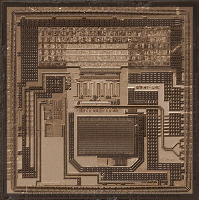
203
ANALOG CIRCUITS AND SIGNAL PROCESSING
 ANALOG CIRCUITS AND SIGNAL PROCESSING Series Editors Mohammed Ismail, The Ohio State University Mohamad Sawan, École Polytechnique de Montréal For further volumes: http://www.springer.com/series/7381 Yongjian
Calibration of current-steering D/A Converters
 Calibration of current-steering D/A Converters Citation for published version (APA): Radulov,. I., Quinn, P. J., Hegt, J. A., & Roermund, van, A. H. M. (2009). Calibration of current-steering D/A Converters.
DESIGN OF MULTI-BIT DELTA-SIGMA A/D CONVERTERS
 DESIGN OF MULTI-BIT DELTA-SIGMA A/D CONVERTERS DESIGN OF MULTI-BIT DELTA-SIGMA A/D CONVERTERS by Yves Geerts Alcatel Microelectronics, Belgium Michiel Steyaert KU Leuven, Belgium and Willy Sansen KU Leuven,
A 14-bit 2.5 GS/s DAC based on Multi-Clock Synchronization. Hegang Hou*, Zongmin Wang, Ying Kong, Xinmang Peng, Haitao Guan, Jinhao Wang, Yan Ren
 Joint International Mechanical, Electronic and Information Technology Conference (JIMET 2015) A 14-bit 2.5 GS/s based on Multi-Clock Synchronization Hegang Hou*, Zongmin Wang, Ying Kong, Xinmang Peng,
On the Study of Improving Noise Shaping Techniques in Wide Bandwidth Sigma Delta Modulators
 On the Study of Improving Noise Shaping Techniques in Wide Bandwidth Sigma Delta Modulators By Du Yun Master Degree in Electrical and Electronics Engineering 2013 Faculty of Science and Technology University
Concepts for smart AD and DA converters
 Concepts for smart AD and DA converters Harpe, P.J.A. DOI: 10.6100/IR656578 Published: 01/01/2010 Document Version Publisher s PDF, also known as Version of Record (includes final page, issue and volume
A novel output transformer based highly linear RF-DAC architecture Bechthum, E.; Radulov, G.I.; Briaire, J.; Geelen, G.; van Roermund, A.H.M.
 A novel output transformer based highly linear RF-DAC architecture Bechthum, E.; Radulov, G.I.; Briaire, J.; Geelen, G.; van Roermund, A.H.M. Published in: Proceedings of the 2st European Conference on
Chapter 2 Basics of Digital-to-Analog Conversion
 Chapter 2 Basics of Digital-to-Analog Conversion This chapter discusses basic concepts of modern Digital-to-Analog Converters (DACs). The basic generic DAC functionality and specifications are discussed,
Fundamentals of Data Converters. DAVID KRESS Director of Technical Marketing
 Fundamentals of Data Converters DAVID KRESS Director of Technical Marketing 9/14/2016 Analog to Electronic Signal Processing Sensor (INPUT) Amp Converter Digital Processor Actuator (OUTPUT) Amp Converter
Lecture 9, ANIK. Data converters 1
 Lecture 9, ANIK Data converters 1 What did we do last time? Noise and distortion Understanding the simplest circuit noise Understanding some of the sources of distortion 502 of 530 What will we do today?
Document Version Publisher s PDF, also known as Version of Record (includes final page, issue and volume numbers)
") A 2V Iductorless Receiver Front-End for Multi-Standard Wireless Applications Vidojkovic, V; Sanduleanu, MAT; van der Tang, JD; Baltus, PGM; van Roermund, AHM Published in: IEEE Radio and Wireless Symposium,
A 2V Iductorless Receiver Front-End for Multi-Standard Wireless Applications Vidojkovic, V; Sanduleanu, MAT; van der Tang, JD; Baltus, PGM; van Roermund, AHM Published in: IEEE Radio and Wireless Symposium,
Appendix A Comparison of ADC Architectures
 Appendix A Comparison of ADC Architectures A comparison of continuous-time delta-sigma (CT ), pipeline, and timeinterleaved (TI) SAR ADCs which target wide signal bandwidths (greater than 100 MHz) and
ISSCC 2004 / SESSION 25 / HIGH-RESOLUTION NYQUIST ADCs / 25.4
 ISSCC 2004 / SESSION 25 / HIGH-RESOLUTION NYQUIST ADCs / 25.4 25.4 A 1.8V 14b 10MS/s Pipelined ADC in 0.18µm CMOS with 99dB SFDR Yun Chiu, Paul R. Gray, Borivoje Nikolic University of California, Berkeley,
Design of 8 Bit Current steering DAC
 Vineet Tiwari 1,Prof.Sanjeev Ranjan 2,Prof. Vivek Baghel 3 1 2 Department of Electronics and Telecommunication Engineering 1 2 Disha Institute of Management & Technology,Raipur,India 3 Department of Electronics
Pipeline vs. Sigma Delta ADC for Communications Applications
 Pipeline vs. Sigma Delta ADC for Communications Applications Noel O Riordan, Mixed-Signal IP Group, S3 Semiconductors noel.oriordan@s3group.com Introduction The Analog-to-Digital Converter (ADC) is a key
Enhancing Analog Signal Generation by Digital Channel Using Pulse-Width Modulation
 Enhancing Analog Signal Generation by Digital Channel Using Pulse-Width Modulation Angelo Zucchetti Advantest angelo.zucchetti@advantest.com Introduction Presented in this article is a technique for generating
Lecture #6: Analog-to-Digital Converter
 Lecture #6: Analog-to-Digital Converter All electrical signals in the real world are analog, and their waveforms are continuous in time. Since most signal processing is done digitally in discrete time,
Chapter 3 Novel Digital-to-Analog Converter with Gamma Correction for On-Panel Data Driver
 Chapter 3 Novel Digital-to-Analog Converter with Gamma Correction for On-Panel Data Driver 3.1 INTRODUCTION As last chapter description, we know that there is a nonlinearity relationship between luminance
Smart AD and DA Conversion
 Smart AD and DA Conversion ANALOG CIRCUITS AND SIGNAL PROCESSING Consulting Editor: Mohammed Ismail. Ohio State University For other titles published in this series, go to www.springer.com/series/7381
Design Strategy for a Pipelined ADC Employing Digital Post-Correction
 Design Strategy for a Pipelined ADC Employing Digital Post-Correction Pieter Harpe, Athon Zanikopoulos, Hans Hegt and Arthur van Roermund Technische Universiteit Eindhoven, Mixed-signal Microelectronics
FUNDAMENTALS OF ANALOG TO DIGITAL CONVERTERS: PART I.1
 FUNDAMENTALS OF ANALOG TO DIGITAL CONVERTERS: PART I.1 Many of these slides were provided by Dr. Sebastian Hoyos January 2019 Texas A&M University 1 Spring, 2019 Outline Fundamentals of Analog-to-Digital
Low-Power Pipelined ADC Design for Wireless LANs
 Low-Power Pipelined ADC Design for Wireless LANs J. Arias, D. Bisbal, J. San Pablo, L. Quintanilla, L. Enriquez, J. Vicente, J. Barbolla Dept. de Electricidad y Electrónica, E.T.S.I. de Telecomunicación,
2.4 A/D Converter Survey Linearity
 2.4 A/D Converter Survey 21 mum and minimum power spectral density (PSD) levels. In the case of a single-channel receiver, this implies the gain control range of the VGA, while in a multi-channel receiver
APPLICATION NOTE 3942 Optimize the Buffer Amplifier/ADC Connection
 Maxim > Design Support > Technical Documents > Application Notes > Communications Circuits > APP 3942 Maxim > Design Support > Technical Documents > Application Notes > High-Speed Interconnect > APP 3942
A 7 bit 3.52 GHz Current Steering DAC for WiGig Applications
 A 7 bit 3.52 GHz Current Steering DAC for WiGig Applications Trindade, M. Helena Abstract This paper presents a Digital to Analog Converter (DAC) with 7 bit resolution and a sampling rate of 3.52 GHz to
CMOS ADC & DAC Principles
 CMOS ADC & DAC Principles Willy Sansen KULeuven, ESAT-MICAS Leuven, Belgium willy.sansen@esat.kuleuven.be Willy Sansen 10-05 201 Table of contents Definitions Digital-to-analog converters Resistive Capacitive
Cascaded Noise-Shaping Modulators for Oversampled Data Conversion
 Cascaded Noise-Shaping Modulators for Oversampled Data Conversion Bruce A. Wooley Stanford University B. Wooley, Stanford, 2004 1 Outline Oversampling modulators for A/D conversion Cascaded noise-shaping
Workshop ESSCIRC. Low-Power Data Acquisition System For Very Small Signals At Low Frequencies With12-Bit- SAR-ADC. 17. September 2010.
 Workshop ESSCIRC Low-Power Data Acquisition System For Very Small Signals At Low Frequencies With12-Bit- SAR-ADC 17. September 2010 Christof Dohmen Outline System Overview Analog-Front-End Chopper-Amplifier
Digital Calibration for Current-Steering DAC Linearity Enhancement
 Digital Calibration for Current-Steering DAC Linearity Enhancement Faculty of Science and Technology, Division of Electronics & Informatics Gunma University Shaiful Nizam Mohyar, Haruo Kobayashi Gunma
A triple-mode continuous-time sigma delta modulator with switched-capacitor feedback DAC for a GSM- EDGE/CDMA2000/UMTS Receiver van Veldhoven, R.H.M.
 A triple-mode continuous-time sigma delta modulator with switched-capacitor feedback DAC for a GSM- EDGE/CDMA2000/UMTS Receiver van Veldhoven, R.H.M. Published in: IEEE Journal of Solid-State Circuits
Design of a Low Power Current Steering Digital to Analog Converter in CMOS
 Design of a Low Power Current Steering Digital to Analog Converter in CMOS Ranjan Kumar Mahapatro M. Tech, Dept. of ECE Centurion University of Technology & Management Paralakhemundi, India Sandipan Pine
Lab.3. Tutorial : (draft) Introduction to CODECs
 Introduction to CODECs") Lab.3. Tutorial : (draft) Introduction to CODECs Fig. Basic digital signal processing system Definition A codec is a device or computer program capable of encoding or decoding a digital data stream or
Lab.3. Tutorial : (draft) Introduction to CODECs Fig. Basic digital signal processing system Definition A codec is a device or computer program capable of encoding or decoding a digital data stream or
IF-Sampling Digital Beamforming with Bit-Stream Processing. Jaehun Jeong
 IF-Sampling Digital Beamforming with Bit-Stream Processing by Jaehun Jeong A dissertation submitted in partial fulfillment of the requirements for the degree of Doctor of Philosophy (Electrical Engineering)
CHAPTER. delta-sigma modulators 1.0
 CHAPTER 1 CHAPTER Conventional delta-sigma modulators 1.0 This Chapter presents the traditional first- and second-order DSM. The main sources for non-ideal operation are described together with some commonly
Sigma-Delta ADC Tutorial and Latest Development in 90 nm CMOS for SoC
 Sigma-Delta ADC Tutorial and Latest Development in 90 nm CMOS for SoC Jinseok Koh Wireless Analog Technology Center Texas Instruments Inc. Dallas, TX Outline Fundamentals for ADCs Over-sampling and Noise
Assoc. Prof. Dr. Burak Kelleci
 DEPARTMENT OF ELECTRICAL &ELECTRONICS ENGINEERING ANALOG-TO-DIGITAL AND DIGITAL- TO-ANALOG CONVERTERS Assoc. Prof. Dr. Burak Kelleci Fall 2018 OUTLINE Nyquist-Rate DAC Thermometer-Code Converter Hybrid
Testing A/D Converters A Practical Approach
 Testing A/D Converters A Practical Approach Mixed Signal The seminar entitled Testing Analog-to-Digital Converters A Practical Approach is a one-day information intensive course, designed to address the
High-Linearity CMOS. RF Front-End Circuits
 High-Linearity CMOS RF Front-End Circuits Yongwang Ding Ramesh Harjani iigh-linearity CMOS tf Front-End Circuits - Springer Library of Congress Cataloging-in-Publication Data A C.I.P. Catalogue record
Receiver Architecture
 Receiver Architecture Receiver basics Channel selection why not at RF? BPF first or LNA first? Direct digitization of RF signal Receiver architectures Sub-sampling receiver noise problem Heterodyne receiver
Integrated Microsystems Laboratory. Franco Maloberti
 University of Pavia Integrated Microsystems Laboratory Power Efficient Data Convertes Franco Maloberti franco.maloberti@unipv.it OUTLINE Introduction Managing the noise power budget Challenges of State-of-the-art
Analysis and Design of 180 nm CMOS Transmitter for a New SBCD Transponder SoC
 WCAS2016 Analysis and Design of 180 nm CMOS Transmitter for a New SBCD Transponder SoC Andrade, N.; Toledo, P.; Cordova, D.; Negreiros, M.; Dornelas, H.; Timbó, R.; Schmidt, A.; Klimach, H.; Frabris, E.
Advantages of Analog Representation. Varies continuously, like the property being measured. Represents continuous values. See Figure 12.
 Analog Signals Signals that vary continuously throughout a defined range. Representative of many physical quantities, such as temperature and velocity. Usually a voltage or current level. Digital Signals
A 3.3-m W sigma delta modular for UMTS in m CMOS with 70-dB dynamic range in 2-MHz bandwidth
 A 3.3-m W sigma delta modular for UMTS in 0.18- m CMOS with 70-dB dynamic range in 2-MHz bandwidth Citation for published version (APA): Veldhoven, van, R. H. M., Minnis, B. J., Hegt, J. A., & Roermund,
Multiple Reference Clock Generator
 A White Paper Presented by IPextreme Multiple Reference Clock Generator Digitial IP for Clock Synthesis August 2007 IPextreme, Inc. This paper explains the concept behind the Multiple Reference Clock Generator
Data Converters. Specifications for Data Converters. Overview. Testing and characterization. Conditions of operation
 Data Converters Overview Specifications for Data Converters Pietro Andreani Dept. of Electrical and Information Technology Lund University, Sweden Conditions of operation Type of converter Converter specifications
Analog and RF circuit techniques in nanometer CMOS
 Analog and RF circuit techniques in nanometer CMOS Bram Nauta University of Twente The Netherlands http://icd.ewi.utwente.nl b.nauta@utwente.nl UNIVERSITY OF TWENTE. Outline Introduction Balun-LNA-Mixer
ADC1006S055/ General description. 2. Features. 3. Applications. Single 10 bits ADC, up to 55 MHz or 70 MHz
 Rev. 03 2 July 2012 Product data sheet 1. General description The are a family of Bipolar CMOS (BiCMOS) 10-bit Analog-to-Digital Converters (ADC) optimized for a wide range of applications such as cellular
12 Bit 1.5 GS/s Return to Zero DAC
 12 Bit 1.5 GS/s Return to Zero DAC RDA112RZ Features 12 Bit Resolution 1.5 GS/s Sampling Rate 10 Bit Static Linearity LVDS Compliant Digital Inputs Power Supply: -5.2V, +3.3V Input Code Format: Offset
A 10 Bit Low Power Current Steering Digital to Analog Converter Using 45 nm CMOS and GDI Logic
 ISSN 2278 0211 (Online) A 10 Bit Low Power Current Steering Digital to Analog Converter Using 45 nm CMOS and GDI Logic Mehul P. Patel M. E. Student (Electronics & communication Engineering) C.U.Shah College
EE247 Lecture 22. Figures of merit (FOM) and trends for ADCs How to use/not use FOM. EECS 247 Lecture 22: Data Converters 2004 H. K.
 and trends for ADCs How to use/not use FOM. EECS 247 Lecture 22: Data Converters 2004 H. K.") EE247 Lecture 22 Pipelined ADCs Combining the bits Stage implementation Circuits Noise budgeting Figures of merit (FOM) and trends for ADCs How to use/not use FOM Oversampled ADCs EECS 247 Lecture 22:
EE247 Lecture 22 Pipelined ADCs Combining the bits Stage implementation Circuits Noise budgeting Figures of merit (FOM) and trends for ADCs How to use/not use FOM Oversampled ADCs EECS 247 Lecture 22:
Solution to Homework 5
 Solution to Homework 5 Problem 1. a- Since (1) (2) Given B=14, =0.2%, we get So INL is the constraint on yield. To meet INL
Architectures and circuits for timeinterleaved. Sandeep Gupta Teranetics, Santa Clara, CA
 Architectures and circuits for timeinterleaved ADC s Sandeep Gupta Teranetics, Santa Clara, CA Outline Introduction to time-interleaved architectures. Conventional Sampling architectures and their application
The Fundamentals of Mixed Signal Testing
 The Fundamentals of Mixed Signal Testing Course Information The Fundamentals of Mixed Signal Testing course is designed to provide the foundation of knowledge that is required for testing modern mixed
A SWITCHED-CAPACITOR POWER AMPLIFIER FOR EER/POLAR TRANSMITTERS
 A SWITCHED-CAPACITOR POWER AMPLIFIER FOR EER/POLAR TRANSMITTERS Sang-Min Yoo, Jeffrey Walling, Eum Chan Woo, David Allstot University of Washington, Seattle, WA Submission Highlight A fully-integrated
AN increasing number of video and communication applications
 1470 IEEE JOURNAL OF SOLID-STATE CIRCUITS, VOL. 32, NO. 9, SEPTEMBER 1997 A Low-Power, High-Speed, Current-Feedback Op-Amp with a Novel Class AB High Current Output Stage Jim Bales Abstract A complementary
NPTEL. VLSI Data Conversion Circuits - Video course. Electronics & Communication Engineering.
 NPTEL Syllabus VLSI Data Conversion Circuits - Video course COURSE OUTLINE This course covers the analysis and design of CMOS Analog-to-Digital and Digital-to-Analog Converters,with about 7 design assigments.
A GHz Quadrature ring oscillator for optical receivers van der Tang, J.D.; Kasperkovitz, D.; van Roermund, A.H.M.
 A 9.8-11.5-GHz Quadrature ring oscillator for optical receivers van der Tang, J.D.; Kasperkovitz, D.; van Roermund, A.H.M. Published in: IEEE Journal of Solid-State Circuits DOI: 10.1109/4.987097 Published:
ISSCC 2001 / SESSION 23 / ANALOG TECHNIQUES / 23.2
 ISSCC 2001 / SESSION 23 / ANALOG TECHNIQUES / 23.2 23.2 Dynamically Biased 1MHz Low-pass Filter with 61dB Peak SNR and 112dB Input Range Nagendra Krishnapura, Yannis Tsividis Columbia University, New York,
Reconfigurable 6 GHz Vector Signal Transceiver with I/Q Interface
 SPECIFICATIONS PXIe-5645 Reconfigurable 6 GHz Vector Signal Transceiver with I/Q Interface Contents Definitions...2 Conditions... 3 Frequency...4 Frequency Settling Time... 4 Internal Frequency Reference...
How to turn an ADC into a DAC: A 110dB THD, 18mW DAC using sampling of the output and feedback to reduce distortion
 How to turn an ADC into a DAC: A 110dB THD, 18mW DAC using sampling of the output and feedback to reduce distortion Axel Thomsen, Design Manager Silicon Laboratories Inc. Austin, TX 1 Why this talk? A
METHODOLOGY FOR THE DIGITAL CALIBRATION OF ANALOG CIRCUITS AND SYSTEMS
 METHODOLOGY FOR THE DIGITAL CALIBRATION OF ANALOG CIRCUITS AND SYSTEMS METHODOLOGY FOR THE DIGITAL CALIBRATION OF ANALOG CIRCUITS AND SYSTEMS with Case Studies by Marc Pastre Ecole Polytechnique Fédérale
A single-slope 80MS/s ADC using two-step time-to-digital conversion
 A single-slope 80MS/s ADC using two-step time-to-digital conversion The MIT Faculty has made this article openly available. Please share how this access benefits you. Your story matters. Citation As Published
Acronyms. ADC analog-to-digital converter. BEOL back-end-of-line
 Acronyms ADC analog-to-digital converter BEOL back-end-of-line CDF cumulative distribution function CMOS complementary metal-oxide-semiconductor CPU central processing unit CR charge-redistribution CS
MSP430 Teaching Materials
 MSP430 Teaching Materials Chapter 9 Data Acquisition A/D Conversion Introduction Texas Instruments t Incorporated University of Beira Interior (PT) Pedro Dinis Gaspar, António Espírito Santo, Bruno Ribeiro,
A Low-Noise Self-Calibrating Dynamic Comparator for High-Speed ADCs
 1 A Low-Noise Self-Calibrating Dynamic Comparator for High-Speed ADCs Masaya Miyahara, Yusuke Asada, Daehwa Paik and Akira Matsuzawa Tokyo Institute of Technology, Japan Outline 2 Motivation The Calibration
ANALYSIS AND DESIGN OF A LOW POWER ADC
 ANALYSIS AND DESIGN OF A LOW POWER ADC MSC. THESIS - VINCENT PETERS - JULY 2012 Supervisors: prof. dr. ir. B. Nauta dr. ing. E.A.M. Klumperink ir. H. Kundur-Subramaniyan dr. ir. A.B.J. Kokkeler Report:
The need for Data Converters
 The need for Data Converters ANALOG SIGNAL (Speech, Images, Sensors, Radar, etc.) PRE-PROCESSING (Filtering and analog to digital conversion) DIGITAL PROCESSOR (Microprocessor) POST-PROCESSING (Digital
TUTORIAL 283 INL/DNL Measurements for High-Speed Analog-to- Digital Converters (ADCs)
") Maxim > Design Support > Technical Documents > Tutorials > A/D and D/A Conversion/Sampling Circuits > APP 283 Maxim > Design Support > Technical Documents > Tutorials > High-Speed Signal Processing > APP
Maxim > Design Support > Technical Documents > Tutorials > A/D and D/A Conversion/Sampling Circuits > APP 283 Maxim > Design Support > Technical Documents > Tutorials > High-Speed Signal Processing > APP
Session 3. CMOS RF IC Design Principles
 Session 3 CMOS RF IC Design Principles Session Delivered by: D. Varun 1 Session Topics Standards RF wireless communications Multi standard RF transceivers RF front end architectures Frequency down conversion
ISSN:
 1391 DESIGN OF 9 BIT SAR ADC USING HIGH SPEED AND HIGH RESOLUTION OPEN LOOP CMOS COMPARATOR IN 180NM TECHNOLOGY WITH R-2R DAC TOPOLOGY AKHIL A 1, SUNIL JACOB 2 1 M.Tech Student, 2 Associate Professor,
Design of Pipeline Analog to Digital Converter
 Design of Pipeline Analog to Digital Converter Vivek Tripathi, Chandrajit Debnath, Rakesh Malik STMicroelectronics The pipeline analog-to-digital converter (ADC) architecture is the most popular topology
ADC1206S040/055/ General description. 2. Features. 3. Applications. Single 12 bits ADC, up to 40 MHz, 55 MHz or 70 MHz
 Rev. 03 2 July 2012 Product data sheet 1. General description The are a family of BiCMOS 12-bit Analog-to-Digital Converters (ADC) optimized for a wide range of applications such as cellular infrastructures,
A 12-bit Interpolated Pipeline ADC using Body Voltage Controlled Amplifier
 A 12-bit Interpolated Pipeline ADC using Body Voltage Controlled Amplifier Hyunui Lee, Masaya Miyahara, and Akira Matsuzawa Tokyo Institute of Technology, Japan Outline Background Body voltage controlled
SUCCESSIVE approximation register (SAR) analog-todigital
 analog-todigital") 426 IEEE TRANSACTIONS ON CIRCUITS AND SYSTEMS II: EXPRESS BRIEFS, VOL. 62, NO. 5, MAY 2015 A Novel Hybrid Radix-/Radix-2 SAR ADC With Fast Convergence and Low Hardware Complexity Manzur Rahman, Arindam
426 IEEE TRANSACTIONS ON CIRCUITS AND SYSTEMS II: EXPRESS BRIEFS, VOL. 62, NO. 5, MAY 2015 A Novel Hybrid Radix-/Radix-2 SAR ADC With Fast Convergence and Low Hardware Complexity Manzur Rahman, Arindam
Deep-Submicron CMOS Design Methodology for High-Performance Low- Power Analog-to-Digital Converters
 Deep-Submicron CMOS Design Methodology for High-Performance Low- Power Analog-to-Digital Converters Abstract In this paper, we present a complete design methodology for high-performance low-power Analog-to-Digital
Modulator with Op- Amp Gain Compensation for Nanometer CMOS Technologies
 A. Pena Perez, V.R. Gonzalez- Diaz, and F. Maloberti, ΣΔ Modulator with Op- Amp Gain Compensation for Nanometer CMOS Technologies, IEEE Proceeding of Latin American Symposium on Circuits and Systems, Feb.
Frequency Synthesizers for RF Transceivers. Domine Leenaerts Philips Research Labs.
 Frequency Synthesizers for RF Transceivers Domine Leenaerts Philips Research Labs. Purpose Overview of synthesizer architectures for RF transceivers Discuss the most challenging RF building blocks Technology
A Low-Power 6-b Integrating-Pipeline Hybrid Analog-to-Digital Converter
 A Low-Power 6-b Integrating-Pipeline Hybrid Analog-to-Digital Converter Quentin Diduck, Martin Margala * Electrical and Computer Engineering Department 526 Computer Studies Bldg., PO Box 270231 University
A 130mW 100MS/s Pipelined ADC with 69dB SNDR Enabled by Digital Harmonic Distortion Correction. Andrea Panigada, Ian Galton
 A 130mW 100MS/s Pipelined ADC with 69dB SNDR Enabled by Digital Harmonic Distortion Correction Andrea Panigada, Ian Galton University of California at San Diego, La Jolla, CA INTEGRATED SIGNAL PROCESSING
Tuesday, February 22nd, 9:15 11:10. Snorre Aunet Nanoelectronics group Department of Informatics University of Oslo
 Nyquist Digital to Analog Converters Tuesday, February 22nd, 9:15 11:10 Snorre Aunet (sa@ifi.uio.no) Nanoelectronics group Department of Informatics University of Oslo February the 15th 1.1 The ideal data
Summary Last Lecture
 Interleaved ADCs EE47 Lecture 4 Oversampled ADCs Why oversampling? Pulse-count modulation Sigma-delta modulation 1-Bit quantization Quantization error (noise) spectrum SQNR analysis Limit cycle oscillations
AD9772A - Functional Block Diagram
 F FEATURES single 3.0 V to 3.6 V supply 14-Bit DAC Resolution 160 MPS Input Data Rate 67.5 MHz Reconstruction Passband @ 160 MPS 74 dbc FDR @ 25 MHz 2 Interpolation Filter with High- or Low-Pass Response
SP 22.3: A 12mW Wide Dynamic Range CMOS Front-End for a Portable GPS Receiver
 SP 22.3: A 12mW Wide Dynamic Range CMOS Front-End for a Portable GPS Receiver Arvin R. Shahani, Derek K. Shaeffer, Thomas H. Lee Stanford University, Stanford, CA At submicron channel lengths, CMOS is
DATASHEET HI5805. Features. Applications. Ordering Information. Pinout. 12-Bit, 5MSPS A/D Converter. FN3984 Rev 7.00 Page 1 of 12.
 12-Bit, 5MSPS A/D Converter NOT RECOMMENDED FOR NEW DESIGNS NO RECOMMENDED REPLACEMENT contact our Technical Support Center at 1-888-INTERSIL or www.intersil.com/tsc DATASHEET FN3984 Rev 7.00 The HI5805
Architectures and Design Methodologies for Very Low Power and Power Effective A/D Sigma-Delta Converters
 0 Architectures and Design Methodologies for Very Low Power and Power Effective A/D Sigma-Delta Converters F. Maloberti University of Pavia - Italy franco.maloberti@unipv.it 1 Introduction Summary Sigma-Delta
National Instruments Flex II ADC Technology The Flexible Resolution Technology inside the NI PXI-5922 Digitizer
 National Instruments Flex II ADC Technology The Flexible Resolution Technology inside the NI PXI-5922 Digitizer Kaustubh Wagle and Niels Knudsen National Instruments, Austin, TX Abstract Single-bit delta-sigma
Asynchronous SAR ADC: Past, Present and Beyond. Mike Shuo-Wei Chen University of Southern California MWSCAS 2014
 Asynchronous SAR ADC: Past, Present and Beyond Mike Shuo-Wei Chen University of Southern California MWSCAS 2014 1 Roles of ADCs Responsibility of ADC is increasing more BW, more dynamic range Potentially
A 25MS/s 14b 200mW Σ Modulator in 0.18µm CMOS
 UT Mixed-Signal/RF Integrated Circuits Seminar Series A 25MS/s 14b 200mW Σ Modulator in 0.18µm CMOS Pio Balmelli April 19 th, Austin TX 2 Outline VDSL specifications Σ A/D converter features Broadband
THE pressure to reduce cost in mass market communication
 1948 IEEE JOURNAL OF SOLID-STATE CIRCUITS, VOL. 33, NO. 12, DECEMBER 1998 A 10-b, 500-MSample/s CMOS DAC in 0.6 mm Chi-Hung Lin and Klaas Bult Abstract A 10-b current steering CMOS digital-to-analog converter
A 24-GHz Quadrature Receiver Front-end in 90-nm CMOS
 A 24GHz Quadrature Receiver Frontend in 90nm CMOS Törmänen, Markus; Sjöland, Henrik Published in: Proc. 2009 IEEE Asia Pacific Microwave Conference Published: 20090101 Link to publication Citation for
Improvement of Output Impedance Modulation Effect of High Speed DAC
 nternational Conference on Artificial ntelligence and Engineering Applications (AEA 2016) mprovement of Output mpedance Modulation Effect of High Speed DAC Dongmei Zhu a, Xiaodan Zhou b, Jun Liu c, Luncai
A 2GS/s 14-bit currentsteering. technology for wireless transmitter
 This article has been accepted and published on J-STAGE in advance of copyediting. Content is final as presented. A 2GS/s 14-bit currentsteering DAC in 65nm CMOS technology for wireless transmitter Luxun
An All CMOS, 2.4 GHz, Fully Adaptive, Scalable, Frequency Hopped Transceiver
 An All CMOS, 2.4 GHz, Fully Adaptive, Scalable, Frequency Hopped Transceiver Farbod Behbahani John Leete Alexandre Kral Shahrzad Tadjpour Karapet Khanoyan Paul J. Chang Hooman Darabi Maryam Rofougaran
SPT BIT, 30 MSPS, TTL, A/D CONVERTER
 12-BIT, MSPS, TTL, A/D CONVERTER FEATURES Monolithic 12-Bit MSPS Converter 6 db SNR @ 3.58 MHz Input On-Chip Track/Hold Bipolar ±2.0 V Analog Input Low Power (1.1 W Typical) 5 pf Input Capacitance TTL
A 1.9GHz Single-Chip CMOS PHS Cellphone
 A 1.9GHz Single-Chip CMOS PHS Cellphone IEEE JSSC, Vol. 41, No.12, December 2006 William Si, Srenik Mehta, Hirad Samavati, Manolis Terrovitis, Michael Mack, Keith Onodera, Steve Jen, Susan Luschas, Justin
UNIVERSITY OF CALIFORNIA College of Engineering Department of Electrical Engineering And Computer Sciences MULTIFREQUENCY CELL IMPEDENCE MEASUREMENT
 UNIVERSITY OF CALIFORNIA College of Engineering Department of Electrical Engineering And Computer Sciences MULTIFREQUENCY CELL IMPEDENCE MEASUREMENT EE247 Term Project Eddie Ng Mounir Bohsali Professor
A 35 fj 10b 160 MS/s Pipelined- SAR ADC with Decoupled Flip- Around MDAC and Self- Embedded Offset Cancellation
 Y. Zu, C.- H. Chan, S.- W. Sin, S.- P. U, R.P. Martins, F. Maloberti: "A 35 fj 10b 160 MS/s Pipelined-SAR ADC with Decoupled Flip-Around MDAC and Self- Embedded Offset Cancellation"; IEEE Asian Solid-
A 2GHz, 17% tuning range quadrature CMOS VCO with high figure of merit and 0.6 phase error
 Downloaded from orbit.dtu.dk on: Dec 17, 2017 A 2GHz, 17% tuning range quadrature CMOS VCO with high figure of merit and 0.6 phase error Andreani, Pietro Published in: Proceedings of the 28th European
A 100MHz CMOS wideband IF amplifier
 A 100MHz CMOS wideband IF amplifier Sjöland, Henrik; Mattisson, Sven Published in: IEEE Journal of Solid-State Circuits DOI: 10.1109/4.663569 1998 Link to publication Citation for published version (APA):
ISSCC 2003 / SESSION 20 / WIRELESS LOCAL AREA NETWORKING / PAPER 20.5
 ISSCC 2003 / SESSION 20 / WIRELESS LOCAL AREA NETWORKING / PAPER 20.5 20.5 A 2.4GHz CMOS Transceiver and Baseband Processor Chipset for 802.11b Wireless LAN Application George Chien, Weishi Feng, Yungping