ANALYZING OF SWITCHING PROPERTIES OF IGBT TRANSISTOR USING PSCAD-EMTDC SIMULATION PROGRAM
|
|
|
- Zoe Ryan
- 6 years ago
- Views:
Transcription
1 2 ANALYZING OF SWITCHING POPETIES OF IGBT TANSISTO USING PSCAD-EMTDC SIMULATION POGAM CUNŢAN Corina Daniela BACIU Ioan UNIVESITATEA POLITEHNICA TIMIŞOAA, FACULTATEA DE INGINEIE HUNEDOAA ABSTACT In this paper is presented functioning of the IGBT transistor in switching process, being presented mathematical model for those two stages, on and off. Based on this model result on equivalent scheme of IGBT transistor, which is tested with PSCAD-EMTDC simulation program. KEYWODS transistor IGBT, simulation, switching. INTODUCTION The IGBT Transistor is an integrat monolithic structure, which contains, in Darlington connexion, a bipolar transistor and a MOSFET one, which need a simple command and which has a reduced value of the voltage drop collector-emitter in conduction at saturation. The duration of getting into conduction of the IGBT corresponds to the time necessary for getting into conduction of the bipolar transistor, and its blocking is made in a longer time than the one of a separate bipolar transistor, because the charge stocked in the base's junction is eliminated more slower. The speed of cancelling the current is reduced and is similar with the one of the collector current from an usual bipolar transistor, when the base is open (the MOSFET transistorul is blocked long before the bipolar transistor). 2. WOK'S PESENTATION In this work is studied the funcitioning of the transistor into a simple circuit fed from a continuous voltage source, having a L charge circuit. I tis achieved a mathematic model of the collector-emitter junction for the IGBT transistor in the commutation process in the two situations: blocking in conduction at saturation and, in revers, from saturation to blocking.
2 In fig..a. is shown the electric diagram of a simple circuit with IGBT and in fig..b the equivalent electric diagram of the circuit shown in fig..a. E L IGB L E C E/ sl I( ) E T /s I (s ) I 2 (s ) /s C a) b) c) Fig. In order to determine the current through the circuit, will be used the Laplace transformation method, in fig..c, being presented the equivalent electric diagram of the circuit in operational. The equation for I(s) is obtained by solving the equation system (). E = s E = s I ( sl)() I s I () s ( sl)() I s I () s () s = I () s I () s 2 2 sc E s T () For I(s) results the following equation: I () s E C T = (2) s Ex. numerical: E E [( sl)( sc ) ] ( sl)( sc ) I = s ( s s 20) s s 20 Using the MATHCAD programming menu, is obtained the equation (3) for the expression of the current in real field. 69
3 i(t) = e (. 00. ) t. cosh t C C. (. 00. ) sinh t C C C C 0. e 0. e /( 0. ) ( C C. 00. ) t C C ( C C ) t C C (3) For =0Ω, C=0-8 F, i(t ) = e ( t) (. cosh( t ) sinh( t )) e ( t) e ( t) By using a program written in Matlab, will be drawn the graphic of the current shape for the values considered in the situation of switching from blocking to conduction, following to repeat the procedure for the switching situation in reverse. In fig. 2.a, is shown the variation form of the current at the switching blocked-saturated and in fig. 2.b the variation form of the current for the switching saturated-blocked. The obtained results will be compared with the wave shapes obtained in an identical circuit with the one presented in fig. and achieved by simulation with the PSCAD EMTDC program. 70
 Fig.")
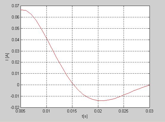
4 a) Fig.2 b) Fig.3 a) 7
 From the analysis of the two graphics, we find a longer time for the switching to blocking, which imposes that in the current's circuit to be provided some protection circuits, especially to")
5 In fig. 3.a is shown the circuit achieved in PSCAD EMTDC and in fig. 3.b. the wave shape which is corresponding to the curent through the circuit. Fig.3 b) From the analysis of the two graphics, we find a longer time for the switching to blocking, which imposes that in the current's circuit to be provided some protection circuits, especially to strongly inductive charges. The protection effect which is connected on the transistor can be seen on the graphic from fig. 4 and in the mathematic model the protection circuit is found included in the value of the capacitor from the equivalent electric diagram. It can be seen a similarity of the two situations concerning the shape of the current in the case of the proposed equivalent circuit and in the one resulted by simulation with the PSCAD EMTDC program. 72

6 CONCLUSIONS: Analysis of the functioning of the IGBT transistor monitors its behavior only in the power part, without studying also its effect on the control circuit. The proposed mathematic model approximates quite well the behavior in switching of the transistor, emphasizing the delay especially at blocking, the effect being more pronounced as the collector current is higher, or the charge circuit's inductance de sarcină has a higher value. EFEENCES: Fig.4. Şora C., Bazele electrotehnicii, Editura D.P. Bucuresti,983; 2. Viorel Popoescu., Electronică de putere; Editura de Vest, Timişoara, 998; 3. Alexa D.,Hrubaru O., Aplicaţii ale convertoarelor statice de putere; Editura Tehnică, Bucureşti, Nicolae P.M., Calitatea energiei electrice in sisteme electroenrgetice de putere limitată, Editura Tehnica, Bucuresti, 998; 5. Chiuta I.. Conecini.N., Compensarea regimului energetic deformat Editura Tehnică, Bucuresti, 989; 6. Lucian Tutelea., Metode de modulare în lpţime de puls pentru invertoare de tensiune, Editura Politehnica, Timişoara, Ghinea A M., Fireţeanu V., Matlab-calcul numeric, grafică, aplicaţii, Editura Teora,
Functioning Analysis of a High Frequency Electro Thermal Installation with Electromagnetic Induction Using PSCAD-EMTDC Tool
 Functioning Analysis of a High Frequency Electro Thermal Installation with Electromagnetic Induction Using PSCAD-EMTDC Tool RALUCA ROB *, IOAN SORA **, CAIUS PANOIU *, MANUELA PANOIU *, * Electrical Engineering
FACULTATEA DE INGINERIE ELECTRICĂ. Ing. Lucian Diodiu. PHD Thesis ABSTRACT
 FACULTATEA DE INGINERIE ELECTRICĂ Ing. Lucian Diodiu PHD Thesis ABSTRACT DETERMINATION OF ENERGY LOSSES IN MEDIUM VOLTAGE TRANSPORT AND DISTRIBUTION ELECTRICAL NETWORKS Thesis advisor, Prof.dr.ing. Nicolae
Researches Regarding the Pollution with Harmonics by the Frequency Converters
 ANALELE UNIVERSITĂłII EFTIMIE MURGU REŞIłA ANUL XV, NR., 008, ISSN 453-7394 Ioan Ruja, Florin Breaban, Ladislau Augustinov, Daniel Jurca Researches Regarding the Pollution with Harmonics by the Frequency
UPON ACHIEVEMENT OF THE USUAL FUNCTIONS OF TIME WITH PS-3 PLC KLÖCKNER- MOELLER
 UPON ACHIEVEMENT OF THE USUAL FUNCTIONS OF TIME WITH PS-3 PLC KLÖCKNER- MOELLER Iosif Popa, Assoc. Prof. PhD. Eng., Faculty of Engineering Hunedoara, Politehnica University Timişoara Gabriel Nicolae Popa,,
Simulation Results on the Currents Harmonics Mitigation on the Railway Station Line Feed
 Proceedings of the 7th WSEAS Int. Conf. on Signal Processing, Computational Geometry & Artificial Vision, Athens, Greece, August 4-6, 7 69 Simulation Results on the Currents Harmonics Mitigation on the
MODELING THE ELECTROMAGNETIC POLLUTION OF THE ELECTRIC ARC FURNACES
 MODELING THE ELECTROMAGNETIC POLLUTION OF THE ELECTRIC ARC FURNACES MANUELA PĂNOIU 1, CAIUS PĂNOIU 2, IOAN ŞORA 3 Key words: Power quality, Electromagnetic pollution, Harmonics, Electric arc furnace (EAF),
MEASUREMENT OF THE PARAMETERS FOR ELECTRIC ENERGY QUALITY. (1) Gabriel VLADUT, (2) Petre-Marian NICOLAE
 Gabriel VLADUT, (2) Petre-Marian NICOLAE") MEASUREMENT OF THE PARAMETERS FOR ELECTRIC ENERGY QUALITY (1) Gabriel VLADUT, (2) Petre-Marian NICOLAE (1)IPA CIFATT Craiova office@ipacv.ro, (2) University of Craiova, pnicolae@elth.ucv.ro Abstract The
MEASUREMENT OF THE PARAMETERS FOR ELECTRIC ENERGY QUALITY (1) Gabriel VLADUT, (2) Petre-Marian NICOLAE (1)IPA CIFATT Craiova office@ipacv.ro, (2) University of Craiova, pnicolae@elth.ucv.ro Abstract The
Using LabVIEW Tool for Verifying the Functioning of an Electronic Programmable Circuit
 Using LabVIEW Tool for Verifying the Functioning of an Electronic Programmable Circuit Corina Daniela Cunţan, Ioan Baciu, Caius Panoiu, Raluca Rob Abstract This paper presents an electronic circuit that
Programmable Encoder Designed in LabVIEW
 Programmable Encoder Designed in LabVIEW CORINA DANIELA CUNTAN, IOAN BACIU, CAIUS PANOIU, RALUCA ROB Electrical Engineering and Industrial Informatics Department, Timisoara Polytechnical University, Faculty
LM125 Precision Dual Tracking Regulator
 LM125 Precision Dual Tracking Regulator INTRODUCTION The LM125 is a precision, dual, tracking, monolithic voltage regulator. It provides separate positive and negative regulated outputs, thus simplifying
UNIT 4 BIASING AND STABILIZATION
 UNIT 4 BIASING AND STABILIZATION TRANSISTOR BIASING: To operate the transistor in the desired region, we have to apply external dec voltages of correct polarity and magnitude to the two junctions of the
Electronics Prof. D. C. Dube Department of Physics Indian Institute of Technology, Delhi
 Electronics Prof. D. C. Dube Department of Physics Indian Institute of Technology, Delhi Module No # 05 FETS and MOSFETS Lecture No # 06 FET/MOSFET Amplifiers and their Analysis In the previous lecture
Power Electronics. P. T. Krein
 Power Electronics Day 10 Power Semiconductor Devices P. T. Krein Department of Electrical and Computer Engineering University of Illinois at Urbana-Champaign 2011 Philip T. Krein. All rights reserved.
THE BALANCING OF TOTAL LOSSES IN THREE-LEVELS VOLTAGE SOURCE CONVERTERS
 U.P.B. Sci. Bull., Series C, Vol. 70, Iss. 4, 2008 ISSN 454234x THE BALANCING OF TOTAL LOSSES IN THREELEVELS VOLTAGE SOURCE CONVERTERS Dan FLORICǍU Proiectarea convertoarelor statice de putere trebuie
EBERS Moll Model. Presented by K.Pandiaraj Assistant Professor ECE Department Kalasalingam University
 EBERS Moll Model Presented by K.Pandiaraj Assistant Professor ECE Department Kalasalingam University BJT Device Models The primary function of a model is to predict the behaviour of a device in particular
Workshop Matlab/Simulink in Drives and Power electronics Lecture 4
 Workshop Matlab/Simulink in Drives and Power electronics Lecture 4 : DC-Motor Chopper design SimPowerSystems Ghislain REMY Jean DEPREZ 1 / 20 Workshop Program 8 lectures will be presented based on Matlab/Simulink
Buletinul AGIR nr. 3/2012 iunie-august. Assis. Eng. Ciprian AFANASOV PhD. University "Ştefan cel Mare" Suceava
 STEP-DOWN VOLTAGE CONVERTER FOR STUDENTS STUDY STEP-DOWN VOLTAGE CONVERTER FOR STUDENTS STUDY Assis. Eng. Ciprian AFANASOV PhD University "Ştefan cel Mare" Suceava REZUMAT. În cadrul lucrării s-au s studiat
Electronics Fundamentals BIPOLAR TRANSISTORS. Construction, circuit symbols and biasing examples for NPN and PNP junction transistors.
 IPOLA TANSISTOS onstruction, circuit symbols and biasing examples for NPN and PNP junction transistors Slide 1 xternal bias voltages create an electric field, which pulls electrons (emitted into the base
4.7 k V C 10 V I B. (b) V ma V. 3.3 k ma. (c)
 V ma V. 3.3 k ma. (c)") 380 Chapter 6 Bipolar Junction Transistors (BJTs) Example 6.4 Consider the circuit shown in Fig. 6., which is redrawn in Fig. 6. to remind the reader of the convention employed throughout this book for
380 Chapter 6 Bipolar Junction Transistors (BJTs) Example 6.4 Consider the circuit shown in Fig. 6., which is redrawn in Fig. 6. to remind the reader of the convention employed throughout this book for
SYSTEM OF CONTROLLING THE PROCESS OF STEEL ELABORATION IN DC ELECTRIC ARC FURNACES
 1 SYSTEM OF CONTROLLING THE PROCESS OF STEEL ELABORATION IN DC ELECTRIC ARC FURNACES GHERMAN Petre Lucian, RUSU Nicolae, ANGHEL Stela UNIVERSITY POLITEHNICA OF TIMIŞOARA, FACULTY OF ENGINEERING OF HUNEDOARA,
b b Fig. 1 Transistor symbols
 TRANSISTORS Transistors have three terminals which are referred to as emitter (e), base (b) and collector (c). Fig 1 shows the symbols used for the two types of transistors in common use. c c b b e e npn
Improving Amplifier Voltage Gain
 15.1 Multistage ac-coupled Amplifiers 1077 TABLE 15.3 Three-Stage Amplifier Summary HAND ANALYSIS SPICE RESULTS Voltage gain 998 1010 Input signal range 92.7 V Input resistance 1 M 1M Output resistance
output passes full first (positive) hump and 1/2-scale second hump
 hump and 1/2-scale second hump") 3. For V i > 0, V o 0. For V i < 0, V o V i. The resulting waveform consists only of the negative "humps" of the original cosine wave. Each hump has a duration of 0.5s there is a 0.5s gap between each
3. For V i > 0, V o 0. For V i < 0, V o V i. The resulting waveform consists only of the negative "humps" of the original cosine wave. Each hump has a duration of 0.5s there is a 0.5s gap between each
Choosing the Appropriate Component from Data Sheet Ratings and Characteristics
 Technical Information Choosing the Appropriate Component from Data Sheet Ratings and Characteristics Choosing the Appropriate Component from Data Sheet Ratings and Characteristics This application note
Modulated Field Synchronous Generator for Wind Turbines
 ANALELE UNIVERSITĂłII EFTIMIE MURGU REŞIłA ANUL XX, NR. 2, 2013, ISSN 1453-7397 Petru Chioncel, Cristian Paul Chioncel Modulated Field Synchronous Generator for Wind Turbines This paper presents a modern
SPEED CONTROL OF DC MOTOR USING FOUR-QUADRANT CHOPPER AND BIPOLAR CONTROL STRATEGY
 SPEED CONTROL OF DC MOTOR USING FOUR-QUADRANT CHOPPER AND BIPOLAR CONTROL STRATEGY TEGY Lecturer Eng. Ciprian AFANASOV PhD, Assoc. Prof. Eng. Mihai RAŢĂ PhD, Assoc. Prof. Eng. Leon MANDICI PhD Ştefan cel
Power Semiconductors. Brian K. Johnson and Herbert L. Hess University of Idaho P.O. Box Moscow, ID USA
 Power Semiconductors Brian K. Johnson and Herbert L. Hess University of Idaho P.O. Box 441023 Moscow, ID 83844-1023 USA Transient Simulation Applications Medium to high power applications Converter applications
Switching and Semiconductor Switches
 1 Switching and Semiconductor Switches 1.1 POWER FLOW CONTROL BY SWITCHES The flow of electrical energy between a fixed voltage supply and a load is often controlled by interposing a controller, as shown
Transistors and Applications
 Chapter 17 Transistors and Applications DC Operation of Bipolar Junction Transistors (BJTs) The bipolar junction transistor (BJT) is constructed with three doped semiconductor regions separated by two
PartIIILectures. Multistage Amplifiers
 University of missan Electronic II, Second year 2015-2016 PartIIILectures Assistant Lecture: 1 Multistage and Compound Amplifiers Basic Definitions: 1- Gain of Multistage Amplifier: Fig.(1-1) A general
Lecture 23 Review of Emerging and Traditional Solid State Switches
 Lecture 23 Review of Emerging and Traditional Solid State Switches 1 A. Solid State Switches 1. Circuit conditions and circuit controlled switches A. Silicon Diode B. Silicon Carbide Diodes 2. Control
Microelectronics Circuit Analysis and Design. Differential Amplifier Intro. Differential Amplifier Intro. 12/3/2013. In this chapter, we will:
 Microelectronics Circuit Analysis and Design Donald A. Neamen Chapter 11 Differential Amplifiers In this chapter, we will: Describe the characteristics and terminology of the ideal differential amplifier.
HGTG12N60A4D, HGTP12N60A4D, HGT1S12N60A4DS
 HGTGN6AD, HGTPN6AD, HGT1SN6ADS Data Sheet December 21 6V, SMPS Series N-Channel IGBT with Anti-Parallel Hyperfast Diode The HGTGN6AD, HGTPN6AD and HGT1SN6ADS are MOS gated high voltage switching devices
Modelling and Simulation of Locomotives with Traction Induction Motors and Three Levels Converters
 Proceedings o the 7th WSEAS International Conerence on Systems Theory and Scientiic Computation, Athens, Greece, August 4-6, 007 175 Modelling and Simulation o Locomotives with Traction Induction Motors
UNIT I BIASING OF DISCRETE BJT AND MOSFET PART A
 UNIT I BIASING OF DISCRETE BJT AND MOSFET PART A 1. Why do we choose Q point at the center of the load line? 2. Name the two techniques used in the stability of the q point.explain. 3. Give the expression
The shape of the waveform will be the same, but its level is shifted either upward or downward. The values of the resistor R and capacitor C affect
 Diode as Clamper A clamping circuit is used to place either the positive or negative peak of a signal at a desired level. The dc component is simply added or subtracted to/from the input signal. The clamper
Understanding VCO Concepts
 Understanding VCO Concepts OSCILLATOR FUNDAMENTALS An oscillator circuit can be modeled as shown in Figure 1 as the combination of an amplifier with gain A (jω) and a feedback network β (jω), having frequency-dependent
Lecture 14. Field Effect Transistor (FET) Sunday 26/11/2017 FET 1-1
 Sunday 26/11/2017 FET 1-1") Lecture 14 Field Effect Transistor (FET) Sunday 26/11/2017 FET 1-1 Outline Introduction to FET transistors Types of FET Transistors Junction Field Effect Transistor (JFET) Characteristics Construction
Lecture 14 Field Effect Transistor (FET) Sunday 26/11/2017 FET 1-1 Outline Introduction to FET transistors Types of FET Transistors Junction Field Effect Transistor (JFET) Characteristics Construction
POWER ELECTRONICS. Alpha. Science International Ltd. S.C. Tripathy. Oxford, U.K.
 POWER ELECTRONICS S.C. Tripathy Alpha Science International Ltd. Oxford, U.K. Contents Preface vii 1. SEMICONDUCTOR DIODE THEORY 1.1 1.1 Introduction 1.1 1.2 Charge Densities in a Doped Semiconductor 1.1
SCHMITT TRIGGER. Typical ``real world'' signals consist of a superposition of a ``noise'' signal and a
 SCHMITT TRIGGER Typical ``real world'' signals consist of a superposition of a ``noise'' signal and a signal or signals of interest. For example, the signal at the bottom of Figure 19 shows a superposition
ased Models of Power Semico for the Circuit Simulator S
 ased Models of Power Semico for the Circuit Simulator S R. Kraus, P. Tiirkes*, J. Sigg* University of Bundeswehr Munich, Werner-Heisenberg-Weg 39, D-85577 Neubiberg, Germany Phone: (+49) 89 6004-3665,
MAHARASHTRA STATE BOARD OF TECHNICAL EDUCATION (Autonomous) (ISO/IEC Certified) Summer 2016 EXAMINATIONS.
 (ISO/IEC Certified) Summer 2016 EXAMINATIONS.") Summer 2016 EXAMINATIONS Subject Code: 17321 Model Answer Important Instructions to examiners: 1) The answers should be examined by key words and not as word-to-word as given in the answer scheme. 2) The
Summer 2016 EXAMINATIONS Subject Code: 17321 Model Answer Important Instructions to examiners: 1) The answers should be examined by key words and not as word-to-word as given in the answer scheme. 2) The
Basic Electronics Prof. Dr. Chitralekha Mahanta Department of Electronics and Communication Engineering Indian Institute of Technology, Guwahati
 Basic Electronics Prof. Dr. Chitralekha Mahanta Department of Electronics and Communication Engineering Indian Institute of Technology, Guwahati Module: 3 Field Effect Transistors Lecture-8 Junction Field
Study for the electric arc of alternative current at the single phase welding machine using the Matlab/Simulink environment
 IOP Conference Series: Materials Science and Engineering PAPER OPEN ACCESS Study for the electric arc of alternative current at the single phase welding machine using the Matlab/Simulink environment To
LM125 Precision Dual Tracking Regulator
 LM125 Precision Dual Tracking Regulator INTRODUCTION The LM125 is a precision dual tracking monolithic voltage regulator It provides separate positive and negative regulated outputs thus simplifying dual
Modeling and Simulation of STATCOM
 Modeling and Simulation of STATCOM Parimal Borse, India Dr. A. G. Thosar Associate Professor, India Samruddhi Shaha, India Abstract:- This paper attempts to model and simulate Flexible Alternating Current
ES 330 Electronics II Homework # 2 (Fall 2016 Due Wednesday, September 7, 2016)
") Page1 Name ES 330 Electronics II Homework # 2 (Fall 2016 Due Wednesday, September 7, 2016) Problem 1 (15 points) You are given an NMOS amplifier with drain load resistor R D = 20 k. The DC voltage (V RD
Page1 Name ES 330 Electronics II Homework # 2 (Fall 2016 Due Wednesday, September 7, 2016) Problem 1 (15 points) You are given an NMOS amplifier with drain load resistor R D = 20 k. The DC voltage (V RD
Analysis on IGBT Developments
 Analysis on IGBT Developments Mahato G.C., Niranjan and Waquar Aarif Abu RVS College of Engineering and Technology, Jamshedpur India Abstract Silicon based high power devices continue to play an important
Gechstudentszone.wordpress.com
 UNIT 4: Small Signal Analysis of Amplifiers 4.1 Basic FET Amplifiers In the last chapter, we described the operation of the FET, in particular the MOSFET, and analyzed and designed the dc response of circuits
SPECIFIC SYMPTOMS OF SINGLE-PHASE INVERTERS FAULTS THAT ARE REQUIRED FOR AN EXPERT SYSTEM DESIGN
 U.P.B. Sci. Bull., Series C, Vol. 78, Iss. 1, 2016 ISSN 2286-3540 SPECIFIC SYMPTOMS OF SINGLE-PHASE INVERTERS FAULTS THAT ARE REQUIRED FOR AN EXPERT SYSTEM DESIGN Sergiu Valentin POPESCU 1, Constantin
Features TO-264 E. Symbol Description SGL50N60RUFD Units V CES Collector-Emitter Voltage 600 V V GES Gate-Emitter Voltage ± 20 V Collector T
 Short Circuit Rated IGBT General Description Fairchild's RUFD series of Insulated Gate Bipolar Transistors (IGBTs) provide low conduction and switching losses as well as short circuit ruggedness. The RUFD
Basic Electronics SYLLABUS BASIC ELECTRONICS. Subject Code : 15ELN15/25 IA Marks : 20. Hrs/Week : 04 Exam Hrs. : 03. Total Hrs. : 50 Exam Marks : 80
 SYLLABUS BASIC ELECTRONICS Subject Code : /25 IA Marks : 20 Hrs/Week : 04 Exam Hrs. : 03 Total Hrs. : 50 Exam Marks : 80 Course objectives: The course objective is to make students of all the branches
HGTP7N60C3D, HGT1S7N60C3D, HGT1S7N60C3DS
 A M A A January 1997 SEMICONDUCTOR HGTP7N6C3D, HGT1S7N6C3D, HGT1S7N6C3DS 14A, 6V, UFS Series N-Channel IGBT with Anti-Parallel Hyperfast Diodes Features 14A, 6V at T C = 2 o C 6V Switching SOA Capability
System and equipment for measurement, registration of parameters and analyse of the quality of the electric energy
 System and equipment for measurement, registration of parameters and analyse of the quality of the electric energy Gabriel VLADUT*, Ion PURCARU **, Petre-Marian NICOLAE,*** Camelia COJOCARU* * IPA, Craiova,
Exercises 6.1, 6.2, 6.3 (page 315 on 7 th edition textbook)
") Exercises 6.1, 6.2, 6.3 (page 315 on 7 th edition textbook) Recapitulation and Equivalent Circuit Models Previous slides present first order BJT model. Assumes npn transistor in active mode. Basic relationship
Exercises 6.1, 6.2, 6.3 (page 315 on 7 th edition textbook) Recapitulation and Equivalent Circuit Models Previous slides present first order BJT model. Assumes npn transistor in active mode. Basic relationship
Chapter 3. Bipolar Junction Transistors
 Chapter 3. Bipolar Junction Transistors Outline: Fundamental of Transistor Common-Base Configuration Common-Emitter Configuration Common-Collector Configuration Introduction The transistor is a three-layer
Learning Material Ver 1.1
 Insulated Gate Bipolar Transistor (IGBT) ST2701 Learning Material Ver 1.1 An ISO 9001:2008 company Scientech Technologies Pvt. Ltd. 94, Electronic Complex, Pardesipura, Indore - 452 010 India, + 91-731
EE105 Fall 2015 Microelectronic Devices and Circuits
 EE105 Fall 2015 Microelectronic Devices and Circuits Prof. Ming C. Wu wu@eecs.berkeley.edu 511 Sutardja Dai Hall (SDH) 11-1 Transistor Operating Mode in Amplifiers Transistors are biased in flat part of
Basic Electronics Prof. Dr. Chitralekha Mahanta Department of Electronics and Communication Engineering Indian Institute of Technology, Guwahati
 Basic Electronics Prof. Dr. Chitralekha Mahanta Department of Electronics and Communication Engineering Indian Institute of Technology, Guwahati Module: 3 Field Effect Transistors Lecture-3 MOSFET UNDER
2 Marks - Question Bank. Unit 1- INTRODUCTION
 Two marks 1. What is power electronics? EE6503 POWER ELECTRONICS 2 Marks - Question Bank Unit 1- INTRODUCTION Power electronics is a subject that concerns the applications electronics principles into situations
The Common Source JFET Amplifier
 The Common Source JFET Amplifier Small signal amplifiers can also be made using Field Effect Transistors or FET's for short. These devices have the advantage over bipolar transistors of having an extremely
To Study The MATLAB Simulation Of A Single Phase STATCOM And Transmission Line
 To Study The MATLAB Simulation Of A Single Phase And Transmission Line Mr. Nileshkumar J. Kumbhar Abstract-As an important member of FACTS family, (Static Synchronous Compensator) has got more and more
E B C. Two-Terminal Behavior (For testing only!) TO-92 Case Circuit Symbol
 TO-92 Case Circuit Symbol") Physics 310 Lab 5 Transistors Equipment: Little silver power-supply, little black multimeter, Decade Resistor Box, 1k,, 470, LED, 10k, pushbutton switch, 270, 2.7k, function generator, o scope, two 5.1k
Physics 310 Lab 5 Transistors Equipment: Little silver power-supply, little black multimeter, Decade Resistor Box, 1k,, 470, LED, 10k, pushbutton switch, 270, 2.7k, function generator, o scope, two 5.1k
Tutorial #5: Emitter Follower or Common Collector Amplifier Circuit
 Tutorial #5: Emitter Follower or Common Collector Amplifier Circuit This tutorial will help you to build and simulate a more complex circuit: an emitter follower. The emitter follower or common collector
LOW LEVEL CURRENTS AND VOLTAGES MEASUREMENTS
 LOW LEVEL CURRENTS AND VOLTAGES MEASUREMENTS CĂTĂLIN VOINA 1, SIMONA MORARU 2, ANDREEA COSAC Key words: analogical data, acquisition. This paper presents one modern solution in order to read electrical
ECE321 Electronics I Fall 2006
 ECE321 Electronics I Fall 2006 Professor James E. Morris Lecture 11 31 st October, 2006 Bipolar Junction Transistors (BJTs) 5.1 Device Structure & Physics 5.2 I-V Characteristics Convert 5.1 information
EXPERIMENT 5 CURRENT AND VOLTAGE CHARACTERISTICS OF BJT
 EXPERIMENT 5 CURRENT AND VOLTAGE CHARACTERISTICS OF BJT 1. OBJECTIVES 1.1 To practice how to test NPN and PNP transistors using multimeter. 1.2 To demonstrate the relationship between collector current
Power Amplifiers. Class A Amplifier
 Power Amplifiers The Power amplifiers amplify the power level of the signal. This amplification is done in the last stage in audio applications. The applications related to radio frequencies employ radio
A New ZVS-PWM Full-Bridge Boost Converter
 Western University Scholarship@Western Electronic Thesis and Dissertation Repository March 2012 A New ZVS-PWM Full-Bridge Boost Converter Mohammadjavad Baei The University of Western Ontario Supervisor
Communication Microelectronics (W17)
") Communication Microelectronics (W17) Lecture 4: Bipolar Junction Transistor Assistant Professor Office: C3.315 E-mail: eman.azab@guc.edu.eg 1 Bipolar Junction Transistor (BJT) Physical Structure and I-V
Communication Microelectronics (W17) Lecture 4: Bipolar Junction Transistor Assistant Professor Office: C3.315 E-mail: eman.azab@guc.edu.eg 1 Bipolar Junction Transistor (BJT) Physical Structure and I-V
DOWNLOAD PDF POWER ELECTRONICS DEVICES DRIVERS AND APPLICATIONS
 Chapter 1 : Power Electronics Devices, Drivers, Applications, and Passive theinnatdunvilla.com - Google D Download Power Electronics: Devices, Drivers and Applications By B.W. Williams - Provides a wide
Chapter 8: Field Effect Transistors
 Chapter 8: Field Effect Transistors Transistors are different from the basic electronic elements in that they have three terminals. Consequently, we need more parameters to describe their behavior than
I C I E =I B = I C 1 V BE 0.7 V
 Guide to NPN Amplifier Analysis Jason Woytowich 1. Transistor characteristics A BJT has three operating modes cutoff, active, and saturation. For applications, like amplifiers, where linear characteristics
Bipolar Junction Transistors (BJTs)
") C H A P T E R 6 Bipolar Junction Transistors (BJTs) Figure 6.1 A simplified structure of the npn transistor and pnp transistor. Table 6.1: BJT modes of Operation Mode Cutoff Active Saturation EBJ Reverse
C H A P T E R 6 Bipolar Junction Transistors (BJTs) Figure 6.1 A simplified structure of the npn transistor and pnp transistor. Table 6.1: BJT modes of Operation Mode Cutoff Active Saturation EBJ Reverse
Exercise 6-2. The IGBT EXERCISE OBJECTIVES
 Exercise 6-2 The IGBT EXERCISE OBJECTIVES At the completion of this exercise, you will know the behaviour of the IGBT during switching operation. You will be able to explain how IGBT switching can be improved.
1 Basics V GG. V GS(th) V GE(th) , i C. i D I L. v DS. , v CE V DD V CC. V DS(on) VCE(sat) (IGBT) I t MOSFET MOSFET.
 V GE(th) , i C. i D I L. v DS. , v CE V DD V CC. V DS(on) VCE(sat) (IGBT) I t MOSFET MOSFET.") Reverse operation During reverse operation (Figure 1.10, III rd quadrant) the IGBT collector pn-junction is poled in reverse direction and there is no inverse conductivity, other than with MOSFETs. Although,
Reverse operation During reverse operation (Figure 1.10, III rd quadrant) the IGBT collector pn-junction is poled in reverse direction and there is no inverse conductivity, other than with MOSFETs. Although,
AN OVER-CURRENT PROTECTION OF POWER MODULES USING IGBT
 AN OVER-CURRENT PROTECTION OF POWER MODULES USING IGBT Mincho Rumenov Zhivkov, Georgi Bogomilov Georgiev, Vencislav Cekov Valchev Department of Electronic Engineering and Microelectronics, Technical University
COLLECTOR DRAIN BASE GATE EMITTER. Applying a voltage to the Gate connection allows current to flow between the Drain and Source connections.
 MOSFETS Although the base current in a transistor is usually small (< 0.1 ma), some input devices (e.g. a crystal microphone) may be limited in their output. In order to overcome this, a Field Effect Transistor
Class D Power Amplifiers
 Class D Power Amplifiers A Class D amplifier is a switching amplifier based on pulse-width modulation (PWM) techniques Purpose: high efficiency, 80% - 95%. The reduction of the power dissipated by the
Low Voltage High Current Controlled Rectifier with IGBT A.C Controller on Primary Side of the Transformer
 AU J.T. 6(4):193-198 (Apr. 2003) ow Voltage High Current Controlled Rectifier with IGBT A.C Controller on Primary Side of the Transformer Seshanna Panthala Faculty of Engineering, Assumption University
Q.1: Power factor of a linear circuit is defined as the:
 Q.1: Power factor of a linear circuit is defined as the: a. Ratio of real power to reactive power b. Ratio of real power to apparent power c. Ratio of reactive power to apparent power d. Ratio of resistance
COATED ELECTRODE MANUAL-METAL ARC WELDING WITH HIGH FREQUENCY WELDING INVERTER POWER SOURCES
 6 TH INTERNATIONAL CONFERENCE ON ELECTROMECHANICAL AND POWER SYSTEMS October 4-6, 2007 - Chiinu, Rep.Moldova COATED ELECTRODE MANUAL-METAL ARC WELDING WITH HIGH FREQUENCY WELDING INVERTER POWER SOURCES
Section 4: Operational Amplifiers
 Section 4: Operational Amplifiers Op Amps Integrated circuits Simpler to understand than transistors Get back to linear systems, but now with gain Come in various forms Comparators Full Op Amps Differential
Impedance of HART Transmitters Nesebar, Inc.
 Impedance of HART Transmitters Nesebar, Inc. A 2Wire 420 ma Process Transmitter is essentially a current regulator. The compliance impedance of the regulator is often tens of megohms near DC but drops
INTEGRATED CIRCUITS. AN1221 Switched-mode drives for DC motors. Author: Lester J. Hadley, Jr.
 INTEGRATED CIRCUITS Author: Lester J. Hadley, Jr. 1988 Dec Author: Lester J. Hadley, Jr. ABSTRACT The purpose of this paper is to demonstrate the use of integrated switched-mode controllers, generally
Structure of Actual Transistors
 4.1.3. Structure of Actual Transistors Figure 4.7 shows a more realistic BJT cross-section Collector virtually surrounds entire emitter region This makes it difficult for electrons injected into base to
EE320L Electronics I. Laboratory. Laboratory Exercise #6. Current-Voltage Characteristics of Electronic Devices. Angsuman Roy
 EE320L Electronics I Laboratory Laboratory Exercise #6 Current-Voltage Characteristics of Electronic Devices By Angsuman Roy Department of Electrical and Computer Engineering University of Nevada, Las
M328 version ESR inductance capacitance meter multifunctional tester DIY
 M328 version ESR inductance capacitance meter multifunctional tester DIY About transistor Multifunction Tester: The tester uses 3.7V rechargeable lithium battery (battery model: 14500) powered portable
5.1 BJT Device Structure and Physical Operation
 11/28/2004 section 5_1 BJT Device Structure and Physical Operation blank 1/2 5.1 BJT Device Structure and Physical Operation Reading Assignment: pp. 377-392 Another kind of transistor is the Bipolar Junction
Physics S123 HW 3: Bipolar Transistors I
 S123 HW 3: Bipolar Transistors I 1 Physics S123 HW 3: Bipolar Transistors I Total Points: 18 REV 0; June 27, 2008. DUE Thursday, July 3, 2008 If a question baffles you, email one of us. The fault may lie
Contributions Concerning the Command of the Brushless D.C. Servomotor
 Proceedings of the th WSEAS International Conference on SYSTEMS, Vouliagmeni, Athens, Greece, July -, (pp-) Contributions Concerning the Command of the Brushless D.C. Servomotor GHEORGHE BALUTA and NIKOLAOS
GT50J301 GT50J301 HIGH POWER SWITCHING APPLICATIONS MOTOR CONTROL APPLICATIONS. MAXIMUM RATINGS (Ta = 25 C) EQUIVALENT CIRCUIT
 EQUIVALENT CIRCUIT") TOSHIBA INSULATED GATE BIPOLAR TRANSISTOR SILICON N CHANNEL IGBT GT50J301 GT50J301 HIGH POWER SWITCHING APPLICATIONS MOTOR CONTROL APPLICATIONS Unit: mm Third generation IGBT Enhancement mode type High
TOSHIBA INSULATED GATE BIPOLAR TRANSISTOR SILICON N CHANNEL IGBT GT50J301 GT50J301 HIGH POWER SWITCHING APPLICATIONS MOTOR CONTROL APPLICATIONS Unit: mm Third generation IGBT Enhancement mode type High
STATIC CHARACTERISTICS OF TRANSISTOR
 STAT CHARACTERISTS OF TRANSISTOR OBJECTIVE The purpose of the experiment is to study the characteristics of bipolar transistor in common emitter (CE) configuration. From the characteristic curve it is
Physics 623 Transistor Characteristics and Single Transistor Amplifier Sept. 12, 2017
 Physics 623 Transistor Characteristics and Single Transistor Amplifier Sept. 12, 2017 1 Purpose To measure and understand the common emitter transistor characteristic curves. To use the base current gain
Design and Simulation of Passive Filter
 Chapter 3 Design and Simulation of Passive Filter 3.1 Introduction Passive LC filters are conventionally used to suppress the harmonic distortion in power system. In general they consist of various shunt
IXBX25N250 = 2500V = 25A 3.3V. High Voltage, High Gain BIMOSFET TM Monolithic Bipolar MOS Transistor. Symbol Test Conditions Maximum Ratings
 High Voltage, High Gain BIMOSFET TM Monolithic Bipolar MOS Transistor IXBX25N25 V CES 9 = 25V = 25A V CE(sat) 3.3V Symbol Test Conditions Maximum Ratings V CES = 25 C to 15 C 25 V V CGR = 25 C to 15 C,
Linear Voltage Regulators Power supplies and chargers SMM Alavi, SBU, Fall2017
 Linear Voltage Regulator LVRs can be classified based on the type of the transistor that is used as the pass element. The bipolar junction transistor (BJT), field effect transistor (FET), or metal oxide
The Norwegian University of Science and Technology ENGLISH. EXAM IN TFY 4185 Measurement Technique/Måleteknikk. 1 Dec 2014 Time: 09:00-13:00
 Page 1 of 9 The Norwegian University of Science and Technology ENGLISH Department of Physics Contact person: Name: Patrick Espy Tel: +47 73 55 10 95 (office) or +47 41 38 65 78 (mobile) EXAM IN TFY 4185
THE JFET. Script. Discuss the JFET and how it differs from the BJT. Describe the basic structure of n-channel and p -channel JFETs
 Course: B.Sc. Applied Physical Science (Computer Science) Year & Sem.: Ist Year, Sem - IInd Subject: Electronics Paper No.: V Paper Title: Analog Circuits Lecture No.: 12 Lecture Title: Analog Circuits
Analog Circuits Prof. Jayanta Mukherjee Department of Electrical Engineering Indian Institute of Technology - Bombay
 Analog Circuits Prof. Jayanta Mukherjee Department of Electrical Engineering Indian Institute of Technology - Bombay Week - 08 Module - 04 BJT DC Circuits Hello, welcome to another module of this course