Sigma-Delta Fractional-N Frequency Synthesis
|
|
|
- Nicholas Shaw
- 6 years ago
- Views:
Transcription
1 Sigma-Delta Fractional-N Frequency Synthesis Scott Meninger Michael Perrott Massachusetts Institute of Technology June 7, 2004 Copyright 2004 by Michael H. Perrott All rights reserved.
2 Note: Much of this material is taken from MITOpenCourseWare Course: 6.976
3 Outline Integer-N synthesis - Bandwidth constraints Fractional-N synthesis - Issue of fractional spurs Σ Fractional-N Synthesis - Quantization noise impact on the PLL Recent developments for lowering the impact of quantization noise Conclusions Q&A
4 Bandwidth Constraints for Integer-N Synthesizers 1/T Loop Filter Bandwidth << 1/T ref(t) (1/T = 20 MHz) PFD Loop Filter out(t) Divider N[k] PFD output has a periodicity of 1/T - 1/T = reference frequency Loop filter must have a bandwidth << 1/T - PFD output pulses must be filtered out and average value extracted Closed loop PLL bandwidth often chosen to be a factor of ten lower than 1/T
5 Bandwidth Versus Frequency Resolution 1/T Loop Filter Bandwidth << 1/T ref(t) (1/T = 20 MHz) PFD Loop Filter out(t) Divider N[k] N[k] S out (f) 1/T out(t) frequency resolution = 1/T GHz Frequency resolution set by reference frequency (1/T) - Higher resolution achieved by lowering 1/T
6 Increasing Resolution in Integer-N Synthesizers 1/T Loop Filter Bandwidth << 1/T 20 MHz 100 ref(t) (1/T = 200 khz) PFD Loop Filter out(t) Divider N[k] 9001 N[k] 9000 out(t) frequency resolution = 1/T S out (f) 1/T GHz Use a reference divider to achieve lower 1/T - Leads to a low PLL bandwidth ( < 20 khz here )
7 The Issue of Noise 1/T Loop Filter Bandwidth << 1/T 20 MHz 100 ref(t) (1/T = 200 khz) PFD Loop Filter out(t) Divider N[k] 9001 N[k] 9000 out(t) frequency resolution = 1/T S out (f) 1/T GHz Lower 1/T leads to higher divide value - Increases PFD noise at synthesizer output
8 Background: Classical Linearized PLL Model PFD-referred Noise S En (f) VCO-referred Noise S Φvn (f) -20 db/dec 0 e n (t) 1/T f 0 Φ vn (t) f Φ ref [k] Φ div [k] α π PFD e(t) I cp Charge Pump Divider 1 N H(f) Loop Filter v(t) K V jf VCO Φ out (t) N[k] Classical PLL model - Predicts impact of PFD and VCO referred noise sources - Does not allow straightforward modeling of impact due to dynamic divide value variations More on this shortly
9 Background: Classical Linearized PLL Model PFD-referred Noise S En (f) VCO-referred Noise S Φvn (f) -20 db/dec 0 e n (t) 1/T f 0 Φ vn (t) f Φ ref [k] Φ div [k] α π PFD e(t) I cp Charge Pump Divider 1 N H(f) Loop Filter v(t) K V jf VCO Φ out (t) N[k] Parameterizing in terms of G(f) helps visualize the nature (high-pass or low-pass) and gain of the noise transfer functions
10 Parameterized Version of Classical Model PFD-referred Noise S En (f) e n (t) f o Φ npfd (t) Divider Control of Frequency Setting (assume noiseless for now) 0 1/T 2π N α Φ c (t) f G(f) VCO-referred Noise S Φvn (f) -20 db/dec 0 Φ vn (t) f o f 1-G(f) Φ nvco (t) Φ n (t) Φ out (t) G(f) represents the PLL closed loop dynamics G(f) is low-pass Nature of noise transfer very easily seen from the parameterized model
11 Modeling PFD Noise Multiplication PFD-referred Noise S En (f) 0 e n (t) 1/T f VCO-referred Noise S Φvn (f) -20 db/dec 0 Φ vn (t) f Radians 2 /Hz 0 (f o ) opt α π N 2 S en (f) S Φvn (f) f f o Φ npfd (t) Divider Control of Frequency Setting (assume noiseless for now) Φ c (t) α π N G(f) Φ n (t) f o Φ nvco (t) 1-G(f) Φ out (t) PFD spectral density multiplied by N 2 before influencing PLL output phase noise Radians 2 /Hz S Φnpfd (f) (f o ) opt S Φnvco (f) High divide values high phase noise at low frequencies 0 f
12 Fractional-N Frequency Synthesizers ref(t) (1/T = 20 MHz) PFD Loop Filter out(t) 91 N sd [k] 90 Dithering Modulator N[k] Divider N sd [k] out(t) S out (f) 1/T frequency resolution << 1/T GHz Break constraint that divide value be integer - Dither divide value dynamically to achieve fractional values - Frequency resolution is now arbitrary regardless of 1/T Want high 1/T to allow a high PLL bandwidth
13 Classical Fractional-N Synthesizer Architecture ref(t) PFD e(t) Loop Filter out(t) div(t) N/N+1 frac[k] Accumulator 1-bit carry_out[k] N sd [k] = N + frac[k] Use an accumulator to perform dithering operation - Fractional input value fed into accumulator - Carry out bit of accumulator fed into divider
14 Accumulator Operation clk(t) frac[k] M-bit Accumulator M-bit 1-bit residue[k] carry_out[k] residue[k] frac[k] =.25 carry_out[k] Carry out bit is asserted when accumulator residue reaches or surpasses its full scale value - Accumulator residue increments by input fractional value each clock cycle
15 Fractional-N Synthesizer Signals with N = 4.25 carry_out(t) out(t) div(t) ref(t) e(t) phase error(t) Divide value set at N = 4 most of the time - Resulting frequency offset causes phase error to accumulate - Reset phase error by swallowing a VCO cycle Achieved by dividing by 5 every 4 reference cycles
16 The Issue of Spurious Tones ref(t) PFD e(t) Loop Filter out(t) div(t) N/N+1 frac[k] Accumulator 1-bit carry_out[k] N sd [k] = N + frac[k] PFD error is periodic - Note that actual PFD waveform is series of pulses the sawtooth waveform represents pulse width values over time Periodic error signal creates spurious tones in synthesizer output - Ruins noise performance of synthesizer
17 The Phase Interpolation Technique ref(t) PFD e(t) Loop Filter out(t) div(t) α N/N+1 D/A frac[k] M-bit Accumulator M-bit residue[k] 1-bit carry_out[k] Phase error due to fractional technique is predicted by the instantaneous residue of the accumulator - Cancel out phase error based on accumulator residue
18 The Problem With Phase Interpolation ref(t) PFD e(t) Loop Filter out(t) div(t) α N/N+1 D/A frac[k] M-bit Accumulator M-bit residue[k] 1-bit carry_out[k] Gain matching between PFD error and scaled D/A output must be extremely precise - Any mismatch will lead to spurious tones at PLL output
19 Is There a Better Way?
20 A Better Dithering Method: Sigma-Delta Modulation Time Domain M-bit Input Digital Σ Modulator 1-bit D/A Analog Output Digital Input Spectrum Quantization Noise Frequency Domain Analog Output Spectrum Input Σ Sigma-Delta dithers in a manner such that resulting quantization noise is shaped to high frequencies
21 Linearized Model of Sigma-Delta Modulator r[k] S r (e j2πft )= NTF z=e j2πft STF q[k] x[k] y[k] x[k] y[k] H Σ s (z) z=e j2πft H n (z) S q (e j2πft )= 1 H n (e j2πft ) 2 12 Composed of two transfer functions relating input and noise to output - Signal transfer function (STF) Filters input (generally undesirable) - Noise transfer function (NTF) Filters (i.e., shapes) noise that is assumed to be white
22 Example: Cutler Sigma-Delta Topology x[k] u[k] y[k] H(z) - 1 e[k] Output is quantized in a multi-level fashion Error signal, e[k], represents the quantization error Filtered version of quantization error is fed back to input - H(z) is typically a highpass filter whose first tap value is 1 i.e., H(z) = 1 + a 1 z -1 + a 2 z H(z) 1 therefore has a first tap value of 0 Feedback needs to have delay to be realizable
23 Linearized Model of Cutler Topology x[k] u[k] y[k] x[k] u[k] r[k] y[k] H(z) - 1 e[k] H(z) - 1 e[k] Represent quantizer block as a summing junction in which r[k] represents quantization error - Note: It is assumed that r[k] has statistics similar to white noise - This is a key assumption for modeling often not true!
24 Calculation of Signal and Noise Transfer Functions x[k] u[k] y[k] x[k] u[k] r[k] y[k] H(z) - 1 e[k] H(z) - 1 e[k] Calculate using Z-transform of signals in linearized model - NTF: H n (z) = H(z) - STF: H s (z) = 1
25 Choice of H(z) 8 7 m = 3 6 Magnitude m = 2 m = Frequency (Hz) 1/(2T)
26 Example: First Order Sigma-Delta Modulator Choose NTF to be x[k] u[k] y[k] H(z) - 1 e[k] Plot of output in time and frequency domains with input of 1 Amplitude Magnitude (db) 0 0 Sample Number Frequency (Hz) 1/(2T)
27 Example: Second Order Sigma-Delta Modulator Choose NTF to be x[k] u[k] y[k] H(z) - 1 e[k] Plot of output in time and frequency domains with input of 2 Amplitude 1 0 Magnitude (db) -1 0 Sample Number Frequency (Hz) 1/(2T)
28 Example: Third Order Sigma-Delta Modulator Choose NTF to be x[k] u[k] y[k] H(z) - 1 e[k] Plot of output in time and frequency domains with input of Amplitude Magnitude (db) Sample Number Frequency (Hz) 1/(2T)
29 Observations Low order Sigma-Delta modulators do not appear to produce shaped noise very well - Reason: low order feedback does not properly scramble relationship between input and quantization noise Quantization noise, r[k], fails to be white Higher order Sigma-Delta modulators provide much better noise shaping with fewer spurs - Reason: higher order feedback filter provides a much more complex interaction between input and quantization noise
30 Warning: Higher Order Modulators May Still Have Tones Quantization noise, r[k], is best whitened when a sufficiently exciting input is applied to the modulator - Varying input and high order helps to scramble interaction between input and quantization noise Worst input for tone generation are DC signals that are rational with a low valued denominator - Examples (third order modulator): x[k] = 0.1 x[k] = /1024 Magnitude (db) Magnitude (db) 0 Frequency (Hz) 1/(2T) 0 Frequency (Hz) 1/(2T)
31 Dither The sigma-delta noise shaping analysis assumes a white quantization noise spectrum In order to make the input look sufficiently exciting a dither signal can be added to it Dithering methods are directly taken from sigma-delta ADC and DAC design - This makes sense since the synthesizer is really a DAC (digital to phase) - Most common method is to add a random sequence to the LSB s of the input
32 Cascaded Sigma-Delta Modulator Topologies x[k] Σ M 1 [k] q 1 [k] Σ M 2 [k] q 2 [k] Σ M 3 [k] M 1 1 y 1 [k] y 2 [k] y 3 [k] Digital Cancellation Logic y[k] Multibit output Achieve higher order shaping by cascading low order sections and properly combining their outputs Advantage over single loop approach - Allows pipelining to be applied to implementation High speed or low power applications benefit Disadvantages - Relies on precise matching requirements when combining outputs (not a problem for digital implementations) - Requires multi-bit quantizer for orders > 1 (single loop does not)
33 MASH topology x[k] Σ M 1 [k] r 1 [k] Σ M 2 [k] r 2 [k] Σ M 3 [k] M 1 1 y 1 [k] y 2 [k] y 3 [k] 1-z -1 (1-z -1 ) 2 u[k] y[k] Cascade first order sections Combine their outputs after they have passed through digital differentiators
34 Calculation of STF and NTF for MASH topology x[k] Σ M 1 [k] r 1 [k] Σ M 2 [k] r 2 [k] Σ M 3 [k] M 1 1 y 1 [k] y 2 [k] y 3 [k] 1-z -1 (1-z -1 ) 2 u[k] y[k] Individual output signals of each first order modulator Addition of filtered outputs
35 Calculation of STF and NTF for MASH topology x[k] Σ M 1 [k] r 1 [k] Σ M 2 [k] r 2 [k] Σ M 3 [k] M 1 1 y 1 [k] y 2 [k] y 3 [k] 1-z -1 (1-z -1 ) 2 u[k] y[k] Overall modulator behavior - STF: H s (z) = 1 - NTF: H n (z) = (1 z -1 ) 3
36 Sigma-Delta Frequency Synthesizers F ref F out = M.F F ref ref(t) div(t) N sd [m] PFD e(t) Σ Modulator Charge Pump N[m] Divider Loop Filter M+1 M Σ Quantization Noise v(t) VCO f out(t) Riley et. al., JSSC, May 1993 Use Sigma-Delta modulator rather than accumulator to perform dithering operation - Achieves much better spurious performance than classical fractional-n approach
37 Background: The Need for A Better PLL Model PFD-referred Noise S En (f) VCO-referred Noise S Φvn (f) -20 db/dec 0 e n (t) 1/T f 0 Φ vn (t) f Φ ref [k] Φ div [k] α π PFD e(t) I cp Charge Pump Divider 1 N H(f) Loop Filter v(t) K V jf VCO Φ out (t) Classical PLL model - Predicts impact of PFD and VCO referred noise sources - Does not allow straightforward modeling of impact due to divide value variations N[k] This is a problem when using fractional-n approach
38 A PLL Model Accommodating Divide Value Variations PFD-referred Noise S En (f) VCO-referred Noise S Φvn (f) -20 db/dec Φ ref [k] PFD Tristate: α=1 XOR: α=2 α T 2π 0 e n (t) 1/T e(t) f C.P. I cp Loop Filter H(f) v(t) VCO K V jf 0 Φ vn (t) f Φ out (t) Φ div [k] 1 N nom Φ d [k] Divider 1 T n[k] 2π z-1 z=e j2πft 1 - z-1 See derivation in Perrott et. al., A Modeling Approach for Sigma-Delta Fractional-N Frequency Synthesizers, JSSC, Aug 2002
39 Parameterized Version of New Model Noise Φ jit [k] e spur (t) α T π PFD-referred Noise S En (f) 0 e n (t) 1/T f VCO-referred Noise S Φvn (f) -20 db/dec 0 Φ vn (t) f Ι cpn (t) 1 Ι f o π α Nnom G(f) f o 1-G(f) Φ npfd (t) Φ nvco (t) Divide value variation n[k] n[k] 2π z z -1 G(f) Φ d (t) z=e j2πft F c (t) T G(f) f o Alternate Representation f o 1 jf Φ c (t) Φ c (t) Φ n (t) Φ out (t) D/A and Filter Freq. Phase
40 Divider Impact For Classical Vs Fractional-N Approaches Classical Synthesizer 1 1/T n(t) 1 T n[k] G(f) f o F out (t) D/A and Filter Fractional-N Synthesizer 1 1/T n sd (t) 1 T n sd [k] Dithering Modulator n[k] G(f) f o D/A and Filter F out (t) Note: 1/T block represents sampler (to go from CT to DT)
41 Focus on Sigma-Delta Frequency Synthesizer n[k] F out (t) n sd [k] 1 1/T n sd (t) 1 T n sd [k] Σ n[k] G(f) f o F out (t) freq=1/t D/A and Filter Divide value can take on fractional values - Virtually arbitrary resolution is possible PLL dynamics act like lowpass filter to remove much of the quantization noise
42 Quantifying the Quantization Noise Impact PFD-referred Noise S En (f) VCO-referred Noise S Φvn (f) -20 db/dec n sd [k] S r (e j2πft )= 1 12 NTF STF H s (z) r[k] Σ H n (z) q[k] n[k] z=e j2πft Σ Quantization Noise S q (e j2πft ) 0 2π z z -1 f Φ n [k] z=e j2πft 0 E n (t) f o Φ vn (t) T G(f) Φ tn,pll (t) Φ div (t) Φ out (t) f o 1/T f π α Nnom G(f) 0 f o f 1-G(f) Calculate by simply attaching Sigma-Delta model - We see that quantization noise is integrated and then low-pass filtered before impacting PLL output
43 Summary: Sources of Phase Noise in Σ Synthesis -60 f o = 84 khz In Digital Σ N[k] Σ Noise Parasitic Pole Synth Output Spectral Density (dbc/hz) PFD-referred noise S Φout,En (f) Σ noise S Φout, Σ (f) VCO-referred noise S Φout,vn (f) Charge-pump / Phase Detector / Reference fc khz 100 khz 1 MHz 10 MHz Frequency f 0 1/T - Low-pass filtered by PLL, dominant at low offset frequencies VCO - High-pass filtered by PLL, dominant at high offset frequencies Σ dithered quantization noise - Low-pass filtered by PLL, noise/bandwidth tradeoff exists
44 A quick note on the linearized model Parasitic Pole In Digital Σ N[k] Σ Noise Synth Output Non-linearities break the assumptions of the linear model - The shaped noise can be folded down to lower frequencies due to non-linearities in the synthesizer PFD/Charge-pump design This process is best seen through behavioral simulation fc
45 A Well Designed Sigma-Delta Synthesizer -60 f o = 84 khz Spectral Density (dbc/hz) PFD-referred noise S Φout,En (f) Σ noise S Φout, Σ (f) VCO-referred noise S Φout,vn (f) khz 100 khz 1 MHz 10 MHz Frequency f 0 1/T Order of G(f) is set to equal to the Sigma-Delta order - Sigma-Delta noise falls at -20 db/dec above G(f) bandwidth Bandwidth of G(f) is set low enough such that synthesizer noise is dominated by intrinsic PFD and VCO noise
46 Impact of Increased Sigma-Delta Order m = 2 m = 3 Spectral Density (dbc/hz) PFD-referred noise S Φout,En (f) Σ noise S Φout, Σ (f) VCO-referred noise S Φout,vn (f) khz 100 khz 1 MHz 10 MHz Frequency f 0 1/T Spectral Density (dbc/hz) PFD-referred noise S Φout,En (f) Σ noise S Φout, Σ (f) VCO-referred noise S Φout,vn (f) khz 100 khz 1 MHz 10 MHz f Frequency 0 1/T PFD and VCO noise unaffected Sigma-Delta noise no longer attenuated by G(f) such that a -20 db/dec slope is achieved above its bandwidth
47 Impact of Increased PLL Bandwidth f o = 84 khz f o = 160 khz Spectral Density (dbc/hz) PFD-referred noise S Φout,En (f) Σ noise S Φout, Σ (f) VCO-referred noise S Φout,vn (f) Spectral Density (dbc/hz) PFD-referred noise S Φout,En (f) VCO-referred noise S Φout,vn (f) Σ noise S Φout, Σ (f) khz 100 khz 1 MHz 10 MHz Frequency f 0 1/T khz 100 khz 1 MHz 10 MHz f Frequency 0 1/T Allows more PFD noise to pass through Allows more Sigma-Delta noise to pass through Increases suppression of VCO noise
48 Can the Quantization Noise Impact be reduced?
49 Impact of Increasing the PLL Bandwidth Ref PFD Loop Filter Out Div N/N+1 Frequency Selection M-bit Σ Modulator 1-bit Quantization Noise Spectrum Output Spectrum Noise Frequency Selection F out Σ PLL dynamics Higher PLL bandwidth leads to less quantization noise suppression - There is a direct trade-off between PLL bandwidth and jitter
50 Method 1 of Reducing Quantization Noise ref(t) PFD e(t) Charge Pump Loop Filter v(t) VCO out(t) N phases div(t) Divider Phase Shifting Logic N sd [m] Σ Modulator N[m] Lower quantization step size by switching between multiple phases of the VCO output - Generate phases by using a ring oscillator or delay locked loop Issue: noise induced by mismatch between phases
51 Method 2 of Reducing Quantization Noise ref(t) PFD e(t) Charge Pump D/A Loop Filter v(t) VCO out(t) div(t) Divider N sd [m] Accumulator Residue Carry Out Use classical fractional-n approach of phase interpolation to cancel out quantization noise - Use a D/A converter matched to PFD/Charge Pump output Issue: limited by mismatch between gain of D/A and PFD/Charge Pump output and nonlinearity in D/A
52 Comparison of Approaches Phase shifting - Vertical approach dq = 4 4 I chp T vco Vertical Slicing with B = I chp T vco 2 4 I chp T vco 1 4 I chp T vco 0 4 I chp T vco Charge Pump Output Phase interpolation Charge Pump Output I chp - Horizontal approach dq = 0 I chp 0 T vco T vco T vco T vco 4 4 I chp T vco Horizontal Slicing with B = I chp T vco 2 4 I chp T vco 1 4 I chp T vco T vco T vco T vco T vco T vco 0 4 I chp T vco T vco ε = 0 4 ε = 1 4 ε = 2 4 ε = 3 4 ε = 4 4 dq = Charge Transferred In Dashed Box
53 Comparison of Approaches Phase shifting - Limited by number of phases that can be generated and their mismatch - Ring oscillators have poor phase noise Phase interpolation - Limited by ability to match DAC output to that of the PFD/Charge pump - High spurious noise can result due to DAC nonlinearity Key observation - Phase interpolation allows us to take advantage of advances in DAC design over the last 20 years We can now largely overcome the above limitations!
54 Two Recent Phase Interpolation Methods A Wideband 2.4-GHz Delta-Sigma Fractional-N PLL With 1-Mb/s In-Loop Modulation, Sudhakar Pamarti and Ian Galton, JSSC, Nov Impact of DAC mismatch mitigated by using Σ- modulator rather than accumulator to perform dithering - Impact of DAC nonlinearity mitigated by using mismatch noise shaping techniques - Overall: reliably achieves 20 db noise suppression A Fractional-N frequency synthesizer architecture utilizing a mismatch compensated PFD/DAC structure, Scott Meninger and M.H. Perrott, TCAS II, Nov Utilizes a mismatch compensated PFD/DAC structure - Simulations show that 40 db noise suppression is achievable!
55 Key Element: A PFD/DAC Structure PFD PFD PFD PFD T vco T vco Leverages application of selective delays of parallel PFD outputs to realize the D/A function - No explicit D/A required - Delay of one VCO cycle can be easily achieved using registers clocked by the VCO Illustrate the idea through animation
56 Apply Phase Shift to Two out of the Four PFD s PFD PFD PFD PFD T vco T vco Net horizontal level shifts to halfway point
57 Apply Phase Shift to Three out of the Four PFD s PFD PFD PFD PFD T vco T vco Net horizontal point shifts up DAC function is self-aligned in gain to PFD output!
58 Actual PFD/DAC Implementation Ref Div VCO Register Based Delay Timing Mismatch Compensation and Re-synchronization Φ0 Φ1 PFD0 PFD1 Charge Pump To Loop Filter Swap From Σ B DAC Mismatch Shaping 2 B 2 B Current Sources A current DAC is used, but is self-aligned to PFD output using the phase shifting method just discussed Nonlinearity of the DAC is removed using mismatch noise shaping techniques Note: approach overcomes mismatch limitations of prior art: Y. Dufour, Fractional Division Charge Compensation, US Patent 6,130,561
59 A quick note on simulation Our group has developed some CAD tools for PLL design PLL Design Assistant - GUI tool which returns required open loop PLL parameters for a desired closed loop response - Also performs noise transfer analysis CppSim - A C++ behavioral level simulator - Has a GUI and schematic capture tool for design and simulation of systems URL: -

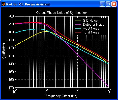
60 PLL Design Assistant

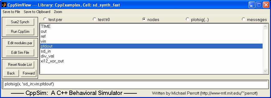

61 CppSim A Fast Behavioral Simulator
62 Goal: Wide bandwidth, low noise synthesizer! Plots below compare classical Σ synth vs. phase interpolation with a 6 bit DAC 36dB Σ noise reduction! BW=1MHz, = 1 BW=1MHz, = 1/64 - Left: Calculated Performance with =1 (classical synth) - Right: Calculated Performance with =1/64
63 Goal: Wide bandwidth, low noise synthesizer! Behavioral simulations verify this is possible (CppSim) 80 Simulated Phase Noise of Freq. Synth Σ Noise Total Noise L(f) (dbc/hz) Frequency Offset from Carrier (Hz) BW=1MHz, = 1/64 BW=1MHz, = 1/64 - Left: Calculated Performance (PLL Design Assistant) - Right: Simulated Performance (CppSim Behavioral)
64 Other Issues to Consider Additional non-idealities must be dealt with - Timing mismatch - Impact of shape of horizontal cancellation waveforms - Impact of both DAC element and timing mismatch sources on achievable spurious performance Note: detailed analytical examination of the above items is difficult - CppSim is an invaluable tool for exploring such issues More details in the paper: A Fractional-N Frequency Synthesizer Architecture Utilizing a Mismatch Compensated PFD/DAC Structure, Scott Meninger, Michael Perrott, TCASII, Nov 2003
65 Conclusions Sigma-Delta Fractional-N Synthesis overcomes the bandwidth limitations of Integer-N synthesis and the spurious limitations of Fractional-N synthesis - Cost is management of the shaped quantization noise Also have to be cautious of tones with the sigma-delta - Can use higher order modulators - Can use dithered input Recent work demonstrates that it is possible to reduce the level of the phase quantization noise using multiphase or multilevel cancellation approach
66 Appendix A sampling of references on Fractional-N, Sigmadelta Fractional-N, and general PLL design - Frequency Synthesis by Phase lock Egan, W.F. - The Design of CMOS Radio Frequency Integrated Circuits Lee, T.H. - Phase Locking in High-Performance Systems edited by Razavi, B. - Monolithic Phase-locked loops and clock recovery circuits edited by Razavi, B. - Delta-Sigma Data Converters edited by Norsworthy, S.R. et. al. Book does not explicitly cover synthesizers, but is a good reference for sigma-delta concepts
6.976 High Speed Communication Circuits and Systems Lecture 17 Advanced Frequency Synthesizers
 6.976 High Speed Communication Circuits and Systems Lecture 17 Advanced Frequency Synthesizers Michael Perrott Massachusetts Institute of Technology Copyright 2003 by Michael H. Perrott Bandwidth Constraints
6.776 High Speed Communication Circuits Lecture 23. Design of Fractional-N Frequency Synthesizers and Bandwidth Extension Techniques
 6.776 High Speed Communication Circuits Lecture 23 Design of Fractional-N Frequency Synthesizers and Bandwidth Extension Techniques Michael Perrott Massachusetts Institute of Technology May, 2005 Copyright
Analog Frequency Synthesizers: A Short Tutorial. IEEE Distinguished Lecture SSCS, Dallas Chapter
 Analog Frequency Synthesizers: A Short Tutorial IEEE Distinguished Lecture SSCS, Dallas Chapter Michael H. Perrott April 2013 Copyright 2013 by Michael H. Perrott All rights reserved. What is a Phase-Locked
High Performance Digital Fractional-N Frequency Synthesizers
 High Performance Digital Fractional-N Frequency Synthesizers Michael Perrott October 16, 2008 Copyright 2008 by Michael H. Perrott All rights reserved. Why Are Digital Phase-Locked Loops Interesting? PLLs
Chapter 2 Analysis of Quantization Noise Reduction Techniques for Fractional-N PLL
 Chapter 2 Analysis of Quantization Noise Reduction Techniques for Fractional-N PLL 2.1 Background High performance phase locked-loops (PLL) are widely used in wireless communication systems to provide
High Performance Digital Fractional-N Frequency Synthesizers. IEEE Distinguished Lecture Lehigh Valley SSCS Chapter
 High Performance Digital Fractional-N Frequency Synthesizers IEEE Distinguished Lecture Lehigh Valley SSCS Chapter Michael H. Perrott October 2013 Copyright 2013 by Michael H. Perrott All rights reserved.
Short Course On Phase-Locked Loops IEEE Circuit and System Society, San Diego, CA. Digital Frequency Synthesizers
 Short Course On Phase-Locked Loops IEEE Circuit and System Society, San Diego, CA Digital Frequency Synthesizers Michael H. Perrott September 6, 2009 Copyright 2009 by Michael H. Perrott All rights reserved.
6.976 High Speed Communication Circuits and Systems Lecture 16 Noise in Integer-N Frequency Synthesizers
 6.976 High Speed Communication Circuits and Systems Lecture 16 in Integer-N Frequency Synthesizers Michael Perrott Massachusetts Institute o Technology Copyright 23 by Michael H. Perrott Frequency Synthesizer
A Low Area, Switched-Resistor Loop Filter Technique for Fractional-N Synthesizers Applied to a MEMS-based Programmable Oscillator
 A Low Area, Switched-Resistor Loop Filter Technique for Fractional-N Synthesizers Applied to a MEMS-based Programmable Oscillator ISSCC 00, Session 3. M.H. Perrott, S. Pamarti, E. Hoffman, F.S. Lee, S.
A VCO-based analog-to-digital converter with secondorder sigma-delta noise shaping
 A VCO-based analog-to-digital converter with secondorder sigma-delta noise shaping The MIT Faculty has made this article openly available. Please share how this access benefits you. Your story matters.
Low Phase Noise, High Bandwidth Frequency Synthesis Techniques. Scott Edward Meninger
 Low Phase Noise, High Bandwidth Frequency Synthesis Techniques by Scott Edward Meninger Bachelor of Science in Electrical Engineering and Computer Science Boston University, June 1996 Master of Science
An analytical phase noise model of charge pump mismatch in sigma-delta frequency synthesizer
 Analog Integr Circ Sig Process (2006) 48:223 229 DOI 10.1007/s10470-006-7832-3 An analytical phase noise model of charge pump mismatch in sigma-delta frequency synthesizer Xiaojian Mao Huazhong Yang Hui
Multiple Reference Clock Generator
 A White Paper Presented by IPextreme Multiple Reference Clock Generator Digitial IP for Clock Synthesis August 2007 IPextreme, Inc. This paper explains the concept behind the Multiple Reference Clock Generator
Short Course On Phase-Locked Loops and Their Applications Day 5, AM Lecture. Advanced PLL Examples (Part I)
") Short Course On Phase-Locked Loops and Their Applications Day 5, AM Lecture Advanced PLL Examples (Part I) Michael Perrott August 15, 2008 Copyright 2008 by Michael H. Perrott All rights reserved. Outline
Short Course On Phase-Locked Loops and Their Applications Day 5, AM Lecture Advanced PLL Examples (Part I) Michael Perrott August 15, 2008 Copyright 2008 by Michael H. Perrott All rights reserved. Outline
CHAPTER. delta-sigma modulators 1.0
 CHAPTER 1 CHAPTER Conventional delta-sigma modulators 1.0 This Chapter presents the traditional first- and second-order DSM. The main sources for non-ideal operation are described together with some commonly
A Wide-Bandwidth 2.4GHz ISM Band Fractional-N PLL with Adaptive Phase Noise Cancellation. Outline
 A Wide-Bandwidth 2.4GHz ISM Band Fractional-N PLL with Adaptive Phase Noise Cancellation Ashok Swaminathan,2, Kevin J. Wang, Ian Galton University of California, San Diego, CA 2 NextWave Broadband, San
Integrated Circuit Design for High-Speed Frequency Synthesis
 Integrated Circuit Design for High-Speed Frequency Synthesis John Rogers Calvin Plett Foster Dai ARTECH H O US E BOSTON LONDON artechhouse.com Preface XI CHAPTER 1 Introduction 1 1.1 Introduction to Frequency
Behavior Model of Noise Phase in a Phase Locked Loop Employing Sigma Delta Modulator
 Behavior Model of Noise Phase in a Phase Locked Loop Employing Sigma Delta Modulator Tayebeh Ghanavati Nejad 1 and Ebrahim Farshidi 2 1,2 Electrical Department, Faculty of Engineering, Shahid Chamran University
Choosing Loop Bandwidth for PLLs
 Choosing Loop Bandwidth for PLLs Timothy Toroni SVA Signal Path Solutions April 2012 1 Phase Noise (dbc/hz) Choosing a PLL/VCO Optimized Loop Bandwidth Starting point for setting the loop bandwidth is
6.976 High Speed Communication Circuits and Systems Lecture 21 MSK Modulation and Clock and Data Recovery Circuits
 6.976 High Speed Communication Circuits and Systems Lecture 21 MSK Modulation and Clock and Data Recovery Circuits Michael Perrott Massachusetts Institute of Technology Copyright 2003 by Michael H. Perrott
ECEN620: Network Theory Broadband Circuit Design Fall 2012
 ECEN620: Network Theory Broadband Circuit Design Fall 2012 Lecture 20: CDRs Sam Palermo Analog & Mixed-Signal Center Texas A&M University Announcements Exam 2 is on Friday Nov. 9 One double-sided 8.5x11
Bluetooth based Synthesizer for Wireless Sensor Measurement Applicable in Health Net Environment
 Bulletin of Environment, Pharmacology and Life Sciences Bull. Env. Pharmacol. Life Sci., Vol 3 [10] September 2014: 99-104 2014 Academy for Environment and Life Sciences, India Online ISSN 2277-1808 Journal
FREQUENCY synthesizers based on phase-locked loops
 IEEE TRANSACTIONS ON CIRCUITS AND SYSTEMS II: EXPRESS BRIEFS, VOL. 54, NO. 8, AUGUST 2007 725 Reduced Complexity MASH Delta Sigma Modulator Zhipeng Ye, Student Member, IEEE, and Michael Peter Kennedy,
Summary Last Lecture
 Interleaved ADCs EE47 Lecture 4 Oversampled ADCs Why oversampling? Pulse-count modulation Sigma-delta modulation 1-Bit quantization Quantization error (noise) spectrum SQNR analysis Limit cycle oscillations
Phase-Locked Loops and Their Applications. Advanced PLL Examples (Part II)
") Short Course On Phase-Locked Loops and Their Applications Day 5, PM Lecture Advanced PLL Examples (Part II) Michael Perrott August 15, 2008 Copyright 2008 by Michael H. Perrott All rights reserved. Outline
Short Course On Phase-Locked Loops and Their Applications Day 5, PM Lecture Advanced PLL Examples (Part II) Michael Perrott August 15, 2008 Copyright 2008 by Michael H. Perrott All rights reserved. Outline
f o Fig ECE 6440 Frequency Synthesizers P.E. Allen Frequency Magnitude Spectral impurity Frequency Fig010-03
 Lecture 010 Introduction to Synthesizers (5/5/03) Page 010-1 LECTURE 010 INTRODUCTION TO FREQUENCY SYNTHESIZERS (References: [1,5,9,10]) What is a Synthesizer? A frequency synthesizer is the means by which
A 0.2-to-1.45GHz Subsampling Fractional-N All-Digital MDLL with Zero-Offset Aperture PD-Based Spur Cancellation and In-Situ Timing Mismatch Detection
 A 0.2-to-1.45GHz Subsampling Fractional-N All-Digital MDLL with Zero-Offset Aperture PD-Based Spur Cancellation and In-Situ Timing Mismatch Detection Somnath Kundu 1, Bongjin Kim 1,2, Chris H. Kim 1 1
INF4420. ΔΣ data converters. Jørgen Andreas Michaelsen Spring 2012
 INF4420 ΔΣ data converters Spring 2012 Jørgen Andreas Michaelsen (jorgenam@ifi.uio.no) Outline Oversampling Noise shaping Circuit design issues Higher order noise shaping Introduction So far we have considered
A Multiphase Compensation Method with Dynamic Element Matching Technique in Σ- Fractional-N Frequency Synthesizers
 JOURNAL OF SEMICONDUCTOR TECHNOLOGY AND SCIENCE, VOL.8, NO.3, SEPTEMBER, 008 179 A Multiphase Compensation Method with Dynamic Element Matching Technique in Σ- Fractional-N Frequency Synthesizers Zuow-Zun
The Case for Oversampling
 EE47 Lecture 4 Oversampled ADCs Why oversampling? Pulse-count modulation Sigma-delta modulation 1-Bit quantization Quantization error (noise) spectrum SQNR analysis Limit cycle oscillations nd order ΣΔ
MULTI-BIT DELTA-SIGMA MODULATION TECHNIQUE FOR FRACTIONAL-N FREQUENCY SYNTHESIZERS WOOGEUN RHEE
 MULTI-BIT DELTA-SIGMA MODULATION TECHNIQUE FOR FRACTIONAL-N FREQUENCY SYNTHESIZERS BY WOOGEUN RHEE B.S., Seoul National University, 1991 M.S., University of California at Los Angeles, 1993 THESIS Submitted
A Wide Tuning Range (1 GHz-to-15 GHz) Fractional-N All-Digital PLL in 45nm SOI
 Fractional-N All-Digital PLL in 45nm SOI") 7- A Wide Tuning Range ( GHz-to-5 GHz) Fractional-N All-Digital PLL in 45nm SOI Alexander Rylyakov, Jose Tierno, George English 2, Michael Sperling 2, Daniel Friedman IBM T. J. Watson Research Center Yorktown
7- A Wide Tuning Range ( GHz-to-5 GHz) Fractional-N All-Digital PLL in 45nm SOI Alexander Rylyakov, Jose Tierno, George English 2, Michael Sperling 2, Daniel Friedman IBM T. J. Watson Research Center Yorktown
Techniques for High-Performance Digital Frequency Synthesis and Phase Control. Chun-Ming Hsu
 Techniques for High-Performance Digital Frequency Synthesis and Phase Control by Chun-Ming Hsu Bachelor of Science in Engineering National Taiwan University, June 1997 Master of Science National Taiwan
A Modeling Approach for 6 1 Fractional-N Frequency Synthesizers Allowing Straightforward Noise Analysis
 1028 IEEE JOURNAL OF SOLID-STATE CIRCUITS, VOL. 37, NO. 8, AUGUST 2002 A Modeling Approach for 6 1 Fractional-N Frequency Synthesizers Allowing Straightforward Noise Analysis Michael H. Perrott, Mitchell
EE247 Lecture 26. EE247 Lecture 26
 EE247 Lecture 26 Administrative Project submission: Project reports due Dec. 5th Please make an appointment with the instructor for a 15minute meeting on Monday Dec. 8 th Prepare to give a 3 to 7 minute
DSM Fractional-N PLLs Spur Optimization
 1. Introduction DSM Fractional-N PLLs Spur Optimization Peregrine s Delta-Sigma modulated (DSM) Fractional-N PLLs include PE9763, PE83363 and some of new products yet to be released. They all have excellent
MAX2769/MAX2769C PLL Loop Filter Calculator User Guide UG6444; Rev 0; 6/17
 MAX2769/MAX2769C PLL Loop Filter Calculator User Guide UG6444; Rev 0; 6/17 Abstract This document briefly covers PLL basics and explains how to use the PLL loop filter spreadsheet calculator for the MAX2769/MAX2769C.
EE247 Lecture 24. EE247 Lecture 24
 EE247 Lecture 24 Administrative EE247 Final exam: Date: Wed. Dec. 15 th Time: -12:30pm-3:30pm- Location: 289 Cory Closed book/course notes No calculators/cell phones/pdas/computers Bring one 8x11 paper
MOST wireless communication systems require local
 IEEE JOURNAL OF SOLID-STATE CIRCUITS, VOL. 43, NO. 12, DECEMBER 2008 2787 Spurious Tone Suppression Techniques Applied to a Wide-Bandwidth 2.4 GHz Fractional-N PLL Kevin J. Wang, Member, IEEE, Ashok Swaminathan,
EE247 Lecture 26. This lecture is taped on Wed. Nov. 28 th due to conflict of regular class hours with a meeting
 EE47 Lecture 6 This lecture is taped on Wed. Nov. 8 th due to conflict of regular class hours with a meeting Any questions regarding this lecture could be discussed during regular office hours or in class
Fractional- N PLL with 90 Phase Shift Lock and Active Switched- Capacitor Loop Filter
 J. Park, F. Maloberti: "Fractional-N PLL with 90 Phase Shift Lock and Active Switched-Capacitor Loop Filter"; Proc. of the IEEE Custom Integrated Circuits Conference, CICC 2005, San Josè, 21 September
ECEN720: High-Speed Links Circuits and Systems Spring 2017
 ECEN720: High-Speed Links Circuits and Systems Spring 2017 Lecture 12: CDRs Sam Palermo Analog & Mixed-Signal Center Texas A&M University Announcements Project Preliminary Report #2 due Apr. 20 Expand
Phase-Locked Loop Engineering Handbook for Integrated Circuits
 Phase-Locked Loop Engineering Handbook for Integrated Circuits Stanley Goldman ARTECH H O U S E BOSTON LONDON artechhouse.com Preface Acknowledgments xiii xxi CHAPTER 1 Cetting Started with PLLs 1 1.1
THE UNIVERSITY OF NAIROBI
 THE UNIVERSITY OF NAIROBI ELECTRICAL AND INFORMATION ENGINEERING DEPARTMENT FINAL YEAR PROJECT. PROJECT NO. 085. TITLE: A PHASE-LOCKED LOOP FREQUENCY SYNTHESIZER BY: TUNDULI W. MICHAEL F17/2143/2004. SUPERVISOR:
Modeling And Implementation of All-Digital Phase-Locked Loop Based on Vernier Gated Ring Oscillator Time-to-Digital Converter
 Master s Thesis Modeling And Implementation of All-Digital Phase-Locked Loop Based on Vernier Gated Ring Oscillator Time-to-Digital Converter Ji Wang Department of Electrical and Information Technology,
264 IEEE TRANSACTIONS ON CIRCUITS AND SYSTEMS I: REGULAR PAPERS, VOL. 58, NO. 2, FEBRUARY 2011
 264 IEEE TRANSACTIONS ON CIRCUITS AND SYSTEMS I: REGULAR PAPERS, VOL. 58, NO. 2, FEBRUARY 2011 A Discrete-Time Model for the Design of Type-II PLLs With Passive Sampled Loop Filters Kevin J. Wang, Member,
ECEN620: Network Theory Broadband Circuit Design Fall 2014
 ECEN620: Network Theory Broadband Circuit Design Fall 2014 Lecture 16: CDRs Sam Palermo Analog & Mixed-Signal Center Texas A&M University Announcements Project descriptions are posted on the website Preliminary
A single-slope 80MS/s ADC using two-step time-to-digital conversion
 A single-slope 80MS/s ADC using two-step time-to-digital conversion The MIT Faculty has made this article openly available. Please share how this access benefits you. Your story matters. Citation As Published
ECEN620: Network Theory Broadband Circuit Design Fall 2012
 ECEN620: Network Theory Broadband Circuit Design Fall 2012 Lecture 11: Charge Pump Circuits Sam Palermo Analog & Mixed-Signal Center Texas A&M University Announcements & Agenda Exam 1 is on Wed. Oct 3
System on a Chip. Prof. Dr. Michael Kraft
 System on a Chip Prof. Dr. Michael Kraft Lecture 5: Data Conversion ADC Background/Theory Examples Background Physical systems are typically analogue To apply digital signal processing, the analogue signal
Telecommunication Electronics
 Politecnico di Torino ICT School Telecommunication Electronics C5 - Special A/D converters» Logarithmic conversion» Approximation, A and µ laws» Differential converters» Oversampling, noise shaping Logarithmic
Phase-Noise Cancellation Design Tradeoffs in Delta Sigma Fractional-N PLLs
 IEEE TRANSACTIONS ON CIRCUITS AND SYSTEMS II: ANALOG AND DIGITAL SIGNAL PROCESSING, VOL. 50, NO. 11, NOVEMBER 2003 829 Phase-Noise Cancellation Design Tradeoffs in Delta Sigma Fractional-N PLLs Sudhakar
Cascaded Noise-Shaping Modulators for Oversampled Data Conversion
 Cascaded Noise-Shaping Modulators for Oversampled Data Conversion Bruce A. Wooley Stanford University B. Wooley, Stanford, 2004 1 Outline Oversampling modulators for A/D conversion Cascaded noise-shaping
High Speed Communication Circuits and Systems Lecture 14 High Speed Frequency Dividers
 High Speed Communication Circuits and Systems Lecture 14 High Speed Frequency Dividers Michael H. Perrott March 19, 2004 Copyright 2004 by Michael H. Perrott All rights reserved. 1 High Speed Frequency
A 60GHz Sub-Sampling PLL Using A Dual-Step-Mixing ILFD
 A 60GHz Sub-Sampling PLL Using A Dual-Step-Mixing ILFD Teerachot Siriburanon, Tomohiro Ueno, Kento Kimura, Satoshi Kondo, Wei Deng, Kenichi Okada, and Akira Matsuzawa Tokyo Institute of Technology, Japan
SPUR REDUCTION TECHNIQUES IN DIRECT DIGITAL SYNTHESIZERS
 Published in the Proceedings of the 1993 International Frequency Control Symposium. SPUR REDUCTION TECHNIQUES IN DIRECT DIGITAL SYNTHESIZERS Victor S. Reinhardt Hughes Space and Communications Company
Summary Last Lecture
 EE47 Lecture 5 Pipelined ADCs (continued) How many bits per stage? Algorithmic ADCs utilizing pipeline structure Advanced background calibration techniques Oversampled ADCs Why oversampling? Pulse-count
Chapter 2 DDSM and Applications
 Chapter DDSM and Applications. Principles of Delta-Sigma Modulation In order to explain the concept of noise shaping in detail, we start with a stand-alone quantizer (see Fig..a) with a small number of
/$ IEEE
 IEEE TRANSACTIONS ON CIRCUITS AND SYSTEMS II: EXPRESS BRIEFS, VOL. 53, NO. 11, NOVEMBER 2006 1205 A Low-Phase Noise, Anti-Harmonic Programmable DLL Frequency Multiplier With Period Error Compensation for
BandPass Sigma-Delta Modulator for wideband IF signals
 BandPass Sigma-Delta Modulator for wideband IF signals Luca Daniel (University of California, Berkeley) Marco Sabatini (STMicroelectronics Berkeley Labs) maintain the same advantages of BaseBand converters
A Straightforward - Fractional-N Phase-Locked Loop HDL Design for RF Applications
 A Straightforward - Fractional-N Phase-Locked Loop HDL Design for RF Applications AHMED EL OUALKADI, DENIS FLANDRE Department of Electrical Engineering Université Catholique de Louvain Maxwell Building,
Chapter 2 Architectures for Frequency Synthesizers
 Chapter 2 Architectures for Frequency Synthesizers 2.1 Overview This chapter starts with an overview of the conventional frequency synthesis techniques as well as the hybrid architectures that can be used
Direct Digital Synthesis Primer
 Direct Digital Synthesis Primer Ken Gentile, Systems Engineer ken.gentile@analog.com David Brandon, Applications Engineer David.Brandon@analog.com Ted Harris, Applications Engineer Ted.Harris@analog.com
A CMOS Frequency Synthesizer with an Injection-Locked Frequency Divider for a 5 GHz Wireless LAN Receiver. Hamid Rategh
 A CMOS Frequency Synthesizer with an Injection-Locked Frequency Divider for a 5 GHz Wireless LAN Receiver Hamid Rategh Center for Integrated Systems Stanford University OUTLINE Motivation Introduction
Introduction to CMOS RF Integrated Circuits Design
 VI. Phase-Locked Loops VI-1 Outline Introduction Basic Feedback Loop Theory Circuit Implementation VI-2 What is a PLL? A PLL is a negative feedback system where an oscillatorgenerated signal is phase and
ECEN620: Network Theory Broadband Circuit Design Fall 2014
 ECEN620: Network Theory Broadband Circuit Design Fall 2014 Lecture 7: Phase Detector Circuits Sam Palermo Analog & Mixed-Signal Center Texas A&M University Announcements & Agenda HW2 is due Oct 6 Exam
ECEN620: Network Theory Broadband Circuit Design Fall 2014
 ECEN60: Network Theory Broadband Circuit Design Fall 014 Lecture 13: Frequency Synthesizer Examples Sam Palermo Analog & Mixed-Signal Center Texas A&M University Agenda Frequency Synthesizer Examples Design
ECEN689: Special Topics in High-Speed Links Circuits and Systems Spring 2010
 ECEN689: Special Topics in High-Speed Links Circuits and Systems Spring 010 Lecture 7: PLL Circuits Sam Palermo Analog & Mixed-Signal Center Texas A&M University Announcements Project Preliminary Report
Analog-to-Digital Converters
 EE47 Lecture 3 Oversampled ADCs Why oversampling? Pulse-count modulation Sigma-delta modulation 1-Bit quantization Quantization error (noise) spectrum SQNR analysis Limit cycle oscillations nd order ΣΔ
National Instruments Flex II ADC Technology The Flexible Resolution Technology inside the NI PXI-5922 Digitizer
 National Instruments Flex II ADC Technology The Flexible Resolution Technology inside the NI PXI-5922 Digitizer Kaustubh Wagle and Niels Knudsen National Instruments, Austin, TX Abstract Single-bit delta-sigma
ECE 627 Project: Design of a High-Speed Delta-Sigma A/D Converter
 ECE 627 Project: Design of a High-Speed Delta-Sigma A/D Converter Brian L. Young youngbr@eecs.oregonstate.edu Oregon State University June 6, 28 I. INTRODUCTION The goal of the Spring 28, ECE 627 project
THE serial advanced technology attachment (SATA) is becoming
 is becoming") IEEE TRANSACTIONS ON CIRCUITS AND SYSTEMS II: EXPRESS BRIEFS, VOL. 54, NO. 11, NOVEMBER 2007 979 A Low-Jitter Spread Spectrum Clock Generator Using FDMP Ding-Shiuan Shen and Shen-Iuan Liu, Senior Member,
IEEE TRANSACTIONS ON CIRCUITS AND SYSTEMS II: EXPRESS BRIEFS, VOL. 54, NO. 11, NOVEMBER 2007 979 A Low-Jitter Spread Spectrum Clock Generator Using FDMP Ding-Shiuan Shen and Shen-Iuan Liu, Senior Member,
Other Effects in PLLs. Behzad Razavi Electrical Engineering Department University of California, Los Angeles
 Other Effects in PLLs Behzad Razavi Electrical Engineering Department University of California, Los Angeles Example of Up and Down Skew and Width Mismatch Approximating the pulses on the control line by
A FREQUENCY SYNTHESIZER STRUCTURE BASED ON COINCIDENCE MIXER
 3 A FREQUENCY SYNTHESIZER STRUCTURE BASED ON COINCIDENCE MIXER Milan STORK University of West Bohemia UWB, P.O. Box 314, 30614 Plzen, Czech Republic stork@kae.zcu.cz Keywords: Coincidence, Frequency mixer,
A 1.9GHz Single-Chip CMOS PHS Cellphone
 A 1.9GHz Single-Chip CMOS PHS Cellphone IEEE JSSC, Vol. 41, No.12, December 2006 William Si, Srenik Mehta, Hirad Samavati, Manolis Terrovitis, Michael Mack, Keith Onodera, Steve Jen, Susan Luschas, Justin
ECEN620: Network Theory Broadband Circuit Design Fall 2014
 ECEN620: Network Theory Broadband Circuit Design Fall 2014 Lecture 8: Charge Pump Circuits Sam Palermo Analog & Mixed-Signal Center Texas A&M University Announcements & Agenda HW2 is due Oct 6 Exam 1 is
Literature Number: SNAP002
 Literature Number: SNAP002 PLL Fundamentals Part 2: PLL Behavior Dean Banerjee Overview General PLL Performance Concepts PLL Loop Theory Lock Time Spurs Phase Noise Fractional PLL Performance Concepts
A 2.2GHZ-2.9V CHARGE PUMP PHASE LOCKED LOOP DESIGN AND ANALYSIS
 A 2.2GHZ-2.9V CHARGE PUMP PHASE LOCKED LOOP DESIGN AND ANALYSIS Diary R. Sulaiman e-mail: diariy@gmail.com Salahaddin University, Engineering College, Electrical Engineering Department Erbil, Iraq Key
ADVANCES in VLSI technology result in manufacturing
 INTL JOURNAL OF ELECTRONICS AND TELECOMMUNICATIONS, 2013, VOL. 59, NO. 1, PP. 99 104 Manuscript received January 8, 2013; revised March, 2013. DOI: 10.2478/eletel-2013-0012 Rapid Prototyping of Third-Order
Phase-Locked Loop Related Terminology & Definitions
 9 Jan 2008 U14063 PLL Terminology.doc 1 Phase-Locked Loop Related Terminology & Definitions References 1. Crawford, J.A., Advanced Phase-Lock Techniques, Artech House, 2007. 2. Crawford, J.A., Frequency
2. ADC Architectures and CMOS Circuits
 /58 2. Architectures and CMOS Circuits Francesc Serra Graells francesc.serra.graells@uab.cat Departament de Microelectrònica i Sistemes Electrònics Universitat Autònoma de Barcelona paco.serra@imb-cnm.csic.es
Improved offline calibration for DAC mismatch in low OSR Sigma Delta ADCs with distributed feedback
 Improved offline calibration for DAC mismatch in low OSR Sigma Delta ADCs with distributed feedback Maarten De Bock, Amir Babaie-Fishani and Pieter Rombouts This document is an author s draft version submitted
A Mostly Digital Variable-Rate Continuous- Time ADC Modulator
 A Mostly Digital Variable-Rate Continuous- Time ADC Modulator Gerry Taylor 1,2, Ian Galton 1 1 University of California at San Diego, La Jolla, CA 2 Analog Devices, San Diego, CA INTEGRATED SIGNAL PROCESSING
Tuesday, March 29th, 9:15 11:30
 Oscillators, Phase Locked Loops Tuesday, March 29th, 9:15 11:30 Snorre Aunet (sa@ifi.uio.no) Nanoelectronics group Department of Informatics University of Oslo Last time and today, Tuesday 29th of March:
Oversampling Converters
 Oversampling Converters Behzad Razavi Electrical Engineering Department University of California, Los Angeles Outline Basic Concepts First- and Second-Order Loops Effect of Circuit Nonidealities Cascaded
A Novel Implementation of Dithered Digital Delta-Sigma Modulators via Bus-Splitting
 B. Fitzgibbon, M.P. Kennedy, F. Maloberti: "A Novel Implementation of Dithered Digital Delta- Sigma Modulators via Bus- Splitting"; IEEE International Symposium on Circuits, ISCAS 211, Rio de Janeiro,
Lecture 160 Examples of CDR Circuits in CMOS (09/04/03) Page 160-1
 Page 160-1") Lecture 160 Examples of CDR Circuits in CMOS (09/04/03) Page 160-1 LECTURE 160 CDR EXAMPLES INTRODUCTION Objective The objective of this presentation is: 1.) Show two examples of clock and data recovery
Lecture 160 Examples of CDR Circuits in CMOS (09/04/03) Page 160-1 LECTURE 160 CDR EXAMPLES INTRODUCTION Objective The objective of this presentation is: 1.) Show two examples of clock and data recovery
EE247 Lecture 26. EE247 Lecture 26
 EE247 Lecture 26 Administrative EE247 Final exam: Date: Mon. Dec. 18 th Time: 12:30pm-3:30pm Location: 241 Cory Hall Extra office hours: Thurs. Dec. 14 th, 10:30am-12pm Closed book/course notes No calculators/cell
5.5: A 3.2 to 4GHz, 0.25µm CMOS Frequency Synthesizer for IEEE a/b/g WLAN
 5.5: A 3.2 to 4GHz, 0.25µm CMOS Frequency Synthesizer for IEEE 802.11a/b/g WLAN Manolis Terrovitis, Michael Mack, Kalwant Singh, and Masoud Zargari 1 Atheros Communications, Sunnyvale, California 1 Atheros
Sigma-Delta ADC Tutorial and Latest Development in 90 nm CMOS for SoC
 Sigma-Delta ADC Tutorial and Latest Development in 90 nm CMOS for SoC Jinseok Koh Wireless Analog Technology Center Texas Instruments Inc. Dallas, TX Outline Fundamentals for ADCs Over-sampling and Noise
SiNANO-NEREID Workshop:
 SiNANO-NEREID Workshop: Towards a new NanoElectronics Roadmap for Europe Leuven, September 11 th, 2017 WP3/Task 3.2 Connectivity RF and mmw Design Outline Connectivity, what connectivity? High data rates
Minimizing Spurious Tones in Digital Delta-Sigma Modulators
 Minimizing Spurious Tones in Digital Delta-Sigma Modulators ANALOG CIRCUITS AND SIGNAL PROCESSING Series Editors: Mohammed Ismail Mohamad Sawan For other titles published in this series, go to http://www.springer.com/series/7381
Fractional N Frequency Synthesis
 Fractional N Frequency Synthesis 1.0 Introduction The premise of fractional N frequency synthesis is to use a feedback (N) counter that can assume fractional values. In many applications, this allows a
Institutionen för systemteknik
 Institutionen för systemteknik Department of Electrical Engineering Examensarbete Investigation of Mechanisms for Spur Generation in Fractional-N Frequency Synthesizers Examensarbete utfört i Elektroniksystem
A 5GHz, 32mW CMOS Frequency Synthesizer with an Injection Locked Frequency Divider. Hamid Rategh, Hirad Samavati, Thomas Lee
 A 5GHz, 32mW CMOS Frequency Synthesizer with an Injection Locked Frequency Divider Hamid Rategh, Hirad Samavati, Thomas Lee OUTLINE motivation introduction synthesizer architecture synthesizer building
Digital Waveform with Jittered Edges. Reference edge. Figure 1. The purpose of this discussion is fourfold.
 Joe Adler, Vectron International Continuous advances in high-speed communication and measurement systems require higher levels of performance from system clocks and references. Performance acceptable in
Understanding Low Phase Noise Signals. Presented by: Riadh Said Agilent Technologies, Inc.
 Understanding Low Phase Noise Signals Presented by: Riadh Said Agilent Technologies, Inc. Introduction Instabilities in the frequency or phase of a signal are caused by a number of different effects. Each
Glossary of VCO terms
 Glossary of VCO terms VOLTAGE CONTROLLED OSCILLATOR (VCO): This is an oscillator designed so the output frequency can be changed by applying a voltage to its control port or tuning port. FREQUENCY TUNING
Taheri: A 4-4.8GHz Adaptive Bandwidth, Adaptive Jitter Phase Locked Loop
 Engineering, Technology & Applied Science Research Vol. 7, No. 2, 2017, 1473-1477 1473 A 4-4.8GHz Adaptive Bandwidth, Adaptive Jitter Phase Locked Loop Hamidreza Esmaeili Taheri Department of Electronics
Design of Bandpass Delta-Sigma Modulators: Avoiding Common Mistakes
 Design of Bandpass Delta-Sigma Modulators: Avoiding Common Mistakes R. Jacob Baker and Vishal Saxena Department of Electrical and Computer Engineering Boise State University 1910 University Dr., ET 201