VK-1 AUDIO OSCILLATOR
|
|
|
- Julius Lawson
- 6 years ago
- Views:
Transcription
1 VK-1 AUDIO OSCILLATOR An audio oscillator is intended for use in audio, therefore the frequency range of its sine wave output should lie between 20Hz and 20kHz. A widened, for example 5Hz-100kHz, range is more preferable, it allows also to investigate some audio circuits whose behavior can be explained by their amplitude and phase responses at the frequencies just outside 20Hz-20kHz. However, this standard audio range is quite sufficient for distortion measurements, it s only important to maintain the oscillator own distortion as low as possible in the whole range, down to 20Hz and up to 20kHz. The main sources of this distortion are the oscillator s active components and some specific passive components in its controlling path. An audio oscillator usually consists of one or several amplifiers and a loop of the positive feedback. Applying this feedback forces the amplifier(s) to start generation which, without control, produces the signal being far from a sinusoid, the signal amplitude quickly reaching a maximum determined only by the supply voltage. To turn the wild generation into stable sine wave oscillation, the negative feedback should be used. It tries to suppress generation, but both opposite processes act simultaneously and, as a result, their equilibrium is finally achieved. The control is performed by the system of amplitude stabilization containing the elements of negative feedback and all the associated circuitry which helps to set the above equilibrium at any desired level of the sine wave output and maintain this level stable. In most simple form, the oscillator can be built around a single operational amplifier, its inputs being the points of applying the signals of positive and negative feedbacks. Both are taken from the oscillator output, the first passes through the Wien bridge network and initiates generation at a certain frequency, the second is regulated by the elements of amplitude stabilization, it makes the amplifier operation linear and its output sinusoidal. All this is illustrated in Fig.1. Fig.1. Wien bridge oscillator. First of all, assume that the op amp A is ideal, i.e. its inverting and non-inverting inputs have the same potential V IN and their input currents are negligibly small. At the negative feedback side we have a simple voltage divider, so R 1 V OUT R 1 + R 2 V IN = V OUT ; K - = = (1) R 1 + R 2 V IN R 1 At the positive feedback side, the Wien bridge network, consisting of the elements R and C, has the following transfer function: 1 R ll sc 1 R K + = , here R ll = parallel connection of resistor R and capacitor C. 1 1 sc RCs + 1 R R ll sc sc Rearrangement of the above expression leads to its final form: R 1 K + = = (2) 1 1 R 2 Cs + 3R RCs sc RCs 1
2 Oscillation takes place when the resulting loop gain becomes unity: K - K + = 1 (3) At the oscillation frequency ω 0 = 1 / RC the Wien bridge network s behavior is very simple: K + = = = = (4) jω ω 0 ω ω 0 j ( 1 1 ) j ( ) + 3 ω 0 jω ω 0 ω The regulated element R 1 of the negative feedback can be therefore calculated from (1) and (4). R 1 + R 2 1 R = 1 ; R 1 = R This element is included in the system of amplitude stabilization whose detector produces from the oscillator output a DC voltage compared then with a reference voltage V 0. The system acts on R 1 and allows to establish any desired, depending on V 0 level of the output V OUT, after that this level being maintained stable. Usually, R 1 is a junction of constant resistors and the electronically variable resistance of such devices as a FET or an optocoupler. In this mode the latter devices are principally non-linear, so it s difficult to minimize distortion contributed by them. The necessary for that reduction of the voltage applied to these devices immediately results in worse static and dynamic stability of the oscillator output. Therefore, the main target of an audio oscillator design is to find a reasonable compromise between low distortion and good stability of its sinusoidal output. It s also important to make the right choice of op amp for the oscillator, but now this seems to be not a problem because a good modern op amp easily ensures its own distortion being well below 0,01% in the whole audio range. Moreover, such op amps are available in packages containing two and four identical devices, so the oscillator can be built on several op amps without notable increase in cost. Advantages of the multistage oscillators are apparent and further I would like to consider such an oscillator with no compromise in performance at all. The chosen topology of this oscillator (see Fig.2) represents its oscillating loop consisting of three op-amp stages two phase-shifting and one inverting. Fig.2. Phase-shifting oscillator. As usual, assume all the op amps are ideal and start the circuit analysis from the first phase-shifting stage. Relationships between its input V IN1 and output V OUT1 voltages can be written with the help of potential V 01 being equal at the inverting and non-inverting inputs of A 1 V IN1 V 01 R 12 R 12 I 01 = ; V OUT1 = V 01 I 01 R 12 = V 01 ( ) V IN (5) R 11 R 11 R 11 The potential V 01 is directly obtained from V IN1 : 2
3 R 1 R 1 C 1 s V 01 = V IN = V IN R 1 C 1 s + 1 R R 12 C 1 s R 1 C 1 s R 11 Substitution V 01 into (5) and subsequent rearrangement give V OUT1 = V IN R 1 C 1 s + 1 V OUT1 R 1 C 1 s - 1 The transfer function of the first stage: K 1 = = , here R 11 = R 12 (6) V IN1 R 1 C 1 s + 1 The same expression in the frequency domain: ω j jωr 1 C 1 1 ω 01 1 K 1 = = , here ω 01 = , it s called the corner frequency of the jωr 1 C ω R 1 C 1 first phase-shifting stage. j ω 01 At the corner frequency (ω = ω 01 ) K 1 = 1 e jφ = 1 e j90º. One extreme frequency value (ω = 0) gives K 1 = -1 = 1 e j180º, other extreme frequency value (ω = ) gives K 1 = 1. Thus, the magnitude of K 1 is always equal 1, while the phase angle between input and output is varying within 0-180º according to the following formula: ω φ 1 = 180º - 2 arctg (7) ω 01 The exact value φ 1 = 90º is reached at ω = ω 01. Similar relationships can be written and for the second phase-shifting stage, on op amp A 2. ω j V OUT2 R 2 C 2 s 1 jωr 2 C 2 1 ω 02 Its transfer function: K 2 = = = = , here R 21 = R 22 (8) V IN2 R 2 C 2 s + 1 jωr 2 C ω j ω 02 1 The corner frequency ω 02 = The magnitude of K 2 is constant (K 2 = 1), its phase shift is R 2 C 2 ω φ 2 = 180º - 2 arctg , (90º at ω = ω 02 ) ω 02 The third stage of the oscillator contains only resistors plus op amp A 3 (see Fig.2). The latter has at its non-inverting input R 34 V 03 = V IN R 33 + R 34 V IN3 V 03 R 31R 34 R 32R 33 The stage output voltage V OUT3 = V 03 I 03 R 33 = V R 32 = V IN , R 31 R 31 (R 33 + R 34 ) V OUT3 R 31 R 34 R 32 R 33 Its transfer function K 3 = = (9) V IN3 R 31 (R 33 + R 34 ) All the three stages are connected in the closed loop, so oscillation will be initiated, if the resulting transfer function or, in other words, closed loop gain becomes equal unity K 1 K 2 K 3 = 1 (10) To satisfy this condition, K 3 must be equal -1, given that earlier calculations have yielded K 1 K 2 = 1 e j90º 1 e j90º = 1 e j180º = -1. Replacing K 1 and K 2 by their expressions (6) and (8) gives an equation for determining the oscillation frequency ω 0 : 3
4 R 1 C 1 s 1 R 2 C 2 s = -1 R 1 C 1 s + 1 R 2 C 2 s + 1 The same after rearrangement R 1 R 2 C 1 C 2 s 2 = -1. Substitution s = jω 0 leads to R 1 R 2 C 1 C 2 ω 0 2 = 1. 1 Finally, the oscillation frequency ω 0 = (11) R 1 R 2 C 1 C 2 When R 1 = R 2 = R and C 1 = C 2 = C, ω 0 = 1/RC. To make the oscillation reliable and optimal in all its parameters, a system of amplitude stabilization is used. Unlike other elaborate systems, it doesn t inject any correction or controlling signal to any point of the circuit, the only element it regulates is a composite resistance R 34 (see Fig.2). Just this resistance is responsible for satisfying the above condition K 1 K 2 K 3 = 1, the automatic variation of R 34 takes place around the value determined from (9) when putting K 3 = -1 : R 33 (R 32 R 31 ) R 34 = (12) 2R 31 The amplitude stabilization is purely parametric and two-channel (precision and dynamic), it s why all characteristics of the output settling time, long-term stability, distortion and noise are predictable and therefore easily controllable. Of course, the oscillator excellent performance first of all should be credited to its topology. Each of the stages has a stable magnitude of its transfer function (K 1 = K 2 = K 3 = 1) regardless of the equality between ω 01 and ω 02 of the phaseshifting stages. This makes it much more easier to maintain the oscillation dynamically stable in amplitude while varying its frequency ω 0 even by a single resistor or capacitor, according to expression (11). If C 1 = C 2 = C and R 1 = R 2 = R, the oscillator delivers the whole set of sinusoids of equal amplitude with relative phases of 0º, 90º and 180º. These outputs can be used for various purposes, in this oscillator they just come in handy in the amplitude stabilization system. The oscillation frequency is usually adjusted by a two-ganged element, potentiometer for example. If this potentiometer has the difference between R 1 and R 2 within 10% (R 2 = 1,1R 1 ), the phase shift φ 1, calculated from (7), will be: ω 0 R 1 C R 1 φ 1 = 180º - 2arctg = 180º - 2arctg = 180º - 2arctg = 180º ,5º = 93º ω 01 C R 1 R 2 R 1 1,1 Here a phase error of 3º is quite tolerable. The third most important feature of this oscillator is that all its regulated elements, both frequency setting (R 1, R 2 ) and amplitude stabilizing (R 34 ), are connected to ground. This means a programmable oscillator can be easily built by replacing the ganged potentiometer with fixed resistors which are switched electronically, with the help of MOSFETs, from a quad SD5200 device for example. Fig.3. Programmable oscillator fragment. Given that all the MOSFETs have their sources connected to ground and their R ON <50Ω is much lower than the switched resistors, the signal applied to their drains doesn t exceed several millivolts, so resulting distortion of the output can be 4
5 expected within 0,001-0,01%. Control circuitry drives the MOSFETs gates according to the required program. Smooth variation of the oscillator frequency can be carried out electronically too, the role of R 1 and R 2 may perform here a twin optocoupler (two photoresistors + LED) or a matched pair of FETs, the latter case being attractive if low distortion isn t of prime importance. In my voltage-controlled oscillator, the twin optocoupler s resistors are involved simultaneously in two processes the AC process of oscillation and DC process of controlling the frequency of this oscillation. To realize such controlling, two current sources produce equal stable currents I 0 which flow through R 1 and R 2 and create DC voltages V 1 and V 2 across them (see Fig.4). Fig.4. Voltage-controlled oscillator. 1 I 0 The frequency of oscillation: f 0 = = , (13) 2πC R 1 R 2 2πC V 1 V 2 so it is determined by these DC voltages which therefore can be used for its accurate setting. Each of them (V 1 and V 2 ) is compared with the same controlling voltage V c, both differences are amplified and the outputs of op amps A 4, A 5 are summed and filtered. The output stage of the frequency setting system, a non-inverting integrator A 6, feeds the optocoupler s LED whose light acts on R 1 and R 2, closing the control loop. The relationship the system maintains with high accuracy is V c = (V 1 + V 2 )/2 and combining it with the above relationship (13) will be simple, if we assume that (V 1 + V 2 )/2 = V 1 V 2. 5
6 I 0 In this case, f 0 = , so the accuracy of controlling the oscillation frequency by the voltage V c depends on 2πCV c matching the values of photoresistors R 1 and R 2, a ±20% matching gives ±0,5% accuracy. To provide optimum parameters of the controlling process, a network of dynamic correction is used. The achieved result is striking a rapid (within 1-2sec) exponential variation of V c from 4V to 4mV causes an immediate, exact log response of frequency from 20Hz to 20kHz. This is particularly important, as the oscillator first of all is intended for use in various sweeping modes. In the VK-1 ultra-low distortion oscillator, the frequency is set manually, on the octave principle which is natural for an oscillator intended for use just in audio. Frequency can be selected from the accurate (1%) basic frequency sequence 20Hz, 40Hz, 80Hz, 160Hz, 315Hz, 630Hz, 1,25kHz, 2,5kHz, 5kHz, 10kHz, 20kHz with the help of an octave rotary switch simultaneously replacing equal capacitors C 1 = C 2 = C of the two phase-shifting stages (see Fig.2). Their resistive elements R 1 and R 2 are switched independently by two additional frequency controls, each of them providing frequency variations in accurate (1%) 1/6, 1/3 or 1/2 octave steps. Joint action of these additional controls gives the resulting variation from the selected basic frequency, it s only should be remembered that the exact 90º phase shift between the oscillator two outputs is guaranteed if R 1 = R 2, i.e. both frequency variations are equal. Choosing both of them, for example, +1/6 octave allows to obtain the next selectable frequency sequence 25Hz, 50Hz, 100Hz, 200Hz, 400Hz, 800Hz, 1,6kHz, 3,15kHz, 6,3kHz, 12,5kHz, 25kHz. And, at last, two +1/3 octave variations give the third standard sequence 31,5Hz, 63Hz, 125Hz, 250Hz, 500Hz, 1kHz, 2kHz, 4kHz, 8kHz, 16kHz, 31,5kHz. Total number of all the spot frequencies is 70 (from 16Hz to 44,8kHz), it s therefore very easy to plot amplitudefrequency responses of the device under test without using a frequency meter. Variation from any above spot frequency can be accomplished within one octave also continuously, by choosing a +(0 1)-octave position of the second additional frequency control switch and turning a fine frequency knob. The varied here is only R 1, a wirewound high-quality potentiometer is used for this purpose. Fine frequency adjustment can be useful, for example, in determining the cut-off frequency of a filter whose behavior in the stop-band area is then investigated by one- or third-octave stepped varying from this frequency. All manipulations with the frequency controls don t cause any notable amplitude bouncing of the output, it is the result of using dynamic amplitude stabilization in the VK-1 oscillator. Typical amplitude stabilization suggests detection of the output sinusoid, filtering and comparing the obtained signal with a DC reference V 0 and then control of the amplitude regulating element, R 1 in the Wien bridge oscillator Fig.1 and R 34 in the phase-shifting oscillator Fig.2. Filtering must be good enough, otherwise the remaining double-frequency ripple modulates the controlling voltage and hence the regulated resistance that leads to appearing the second harmonic of distortion, particularly at the lowest frequencies. Averaging solves this problem, but it introduces a time delay in reaction of the system to a change of amplitude, the regulating element adding to that its own delay (0,1 0,4sec for a photoresistor). The gain within the control loop is very high and the process of amplitude settling hardly can be provided optimal in the whole audio range. To damp appearing oscillation in the amplitude settling at the lowest frequencies, the filter time constant should be increased, but that makes the settling process too slow at high audio frequencies. In oscillators with the decade frequency range selection, a compromise may be found by switching the filter s capacitors according to the chosen frequency range, so the amplitude controlling process always is maintained close to optimum. Another approach is used in my VK-1 oscillator and the described above voltage-controlled oscillator. Each of them contains two channels of amplitude stabilization (precision and dynamic) which act on a single regulating element resistance R 34 (see Fig.2). In the VK-1 oscillator (Fig.5), this resistance is composite, it represents a series connection of stable resistor R 30, photoresistor R PH and the drain-to-source resistance R DS of a FET T 1. Operation of the precision channel is similar to that of the considered earlier typical amplitude stabilization system. Much more higher is its performance, particularly in obtaining the mean-rectified value of the oscillator output. The used precision full-wave synchronous detector contains fast electronic switches which turn on and off exactly at the moments of the output sinusoid zero-crossing. Therefore, the detection accuracy is high in a wide range of voltages (2mV 2V) and frequencies (10Hz-200kHz), the characteristics unreachable when using ordinary diode detectors. The synchronous detector is controlled by a square wave shaper which is built on discrete components and produces two balanced, square wave, very symmetrical outputs with fast rising and falling edges and regulated bipolar swing. The loop of precision amplitude stabilization is closed by the optocoupler LED+R PH, being the most critical element in achieving both the lowest distortion and highest stability. The main thing here is to make the right choice of the optocoupler type and to find its optimal working conditions. The dynamic channel of amplitude stabilization consists of a buffer and a sample-and-hold circuit built around op amp A 6 and controlled by a strobe generator. The latter is triggered by the rising edge of the square wave voltage V SW and produces a short pulse closing an electronic switch S just at the moment the buffer s output sinusoid reaches its maximum. The rest of the period the charged capacitor C 4 serves as a memory of the output amplitude which after buffering (A 6 ) and proper attenuation (R AT ) is applied to the gate of the p-channel FET T 1. An increase of amplitude makes the FET biasing voltage and its drain-to-source resistance higher, that via the control loop leads to reducing the amplitude to its former value. Such compensation is carried out without delays, it takes place in each period of the output frequency and helps the precision channel to maintain the output amplitude stable just during transient periods of operation, ensuring 6
7 its settling process to be always fast aperiodic. Fig.5. VK-1 audio oscillator. In the voltage-controlled oscillator, dynamic operation of the amplitude stabilization system is impressive indeed its two channels act on a single regulating element, a FET T (Fig.4), which performs so tight control of the output, that even this output s fast (1-2sec) frequency sweep from 20Hz to 20kHz doesn t cause any slightest notable disturbance of its amplitude. The precision channel of amplitude stabilization establishes the oscillator output at the level of its mean-rectified value, this level is determined by the reference V 0 and for the VK-1 oscillator it normally equals 2V, for the voltage-controlled oscillator 0,4V. The time constant of integrator A 5 (Fig.5) doesn t heavily affect the system s dynamics anymore, so capacitor C 3 can be chosen for the best filtering the products of detection to eliminate the associated distortion at all. Just the precision channel provides a long-term and temperature stability of the outputs V OUT1 and V OUT2 and their very flat amplitude-frequency characteristic, the accuracy of maintaining these outputs is better than 0,3% under all possible, even extreme conditions. Of course, blameless operation of the amplitude stabilization system requires right and careful adjustment of each its channel and both of them in interaction. Fortunately, the chosen oscillator topology allows to perform this adjustment without any trade-off between low distortion and good stability. The oscillator outputs V OUT1 and V OUT2 have a 90º phase shift between them and each of them can be smoothly variable within 0-2V with the help of a wirewound high-quality potentiometer whose resistance shouldn t be too low to avoid excessive loading of the op amp and rising distortion, at the same time it shouldn t be too high, as it determines the oscillator output impedance. The main output V OUT1 can be also attenuated in 10dB steps from 0dB (1V) down to -60dB (1mV), its output impedance being in this case exactly 600Ω that keeps the attenuation correct regardless of loading. So far, such characteristics of the generated sine wave signal as its amplitude and frequency have been analyzed in detail. It s time however to focus on one more characteristic distortion being most disputable in audio and even ignored by some respected manufacturers who declare only output power and frequency range of their audio products. Assume that we have a nearly ideal automatic rejection filter completely suppressing the fundamental harmonic and leaving absolutely untouched the residuals, an amplifier bringing these residuals, distortion and noise, to a sufficient, 7
8 within 0,1-1V level, a band-pass 20Hz-100kHz filter, a RMS-millivoltmeter, an oscilloscope and, at last, a computer with a decent soundcard and the SpectraLab 4.32 software installed. Connection of this equipment according to Fig.6 gives a typical test scheme for the accurate and thorough distortion analysis. Fig.6. Distortion measurement scheme. The test scheme works excellently while distortion of the oscillator under test is higher than 0,002%. The corresponding curve on the oscilloscope screen looks clear and still, the RMS-millivoltmeter reading THD+N (V) is confidently confirmed by the result of spectrum analysis performed by the computer program, the obtained harmonics of distortion are displayed on the monitor, measured and then combined in a root-sum-square fashion: THD+N (V) (V H2 ) 2 +(V H3 ) 2 +(V H4 ) 2 +(V H5 ) 2, Here the oscillator output noise N, measured in a 20Hz-100kHz bandwidth, is negligible in comparison with the total distortion which in many practical situations can be represented only by its first four harmonic components V H2, V H3, V H4, V H5. To specify distortion in %, it should be expressed with respect to the fundamental signal V S : (V H2 ) 2 +(V H3 ) 2 +(V H4 ) 2 +(V H5 ) 2 THD+N (%) V S When investigating distortion below 0,001%, the oscillator noise becomes the main interfering factor. The observable on the oscilloscope screen distortion curve acquires a noise cover which is getting thicker if distortion is reduced and the vertical sensitivity of the oscilloscope is proportionally increased. In the end, the distortion may become undistinguished at all in the noise background, just this picture is seen when testing the VK-1 audio oscillator at all its frequencies. Only spectrum analysis can discover such vanishingly small distortion and the SpectraLAB 4.32 software allows to register the amplitude of its harmonics down to -145dB. The expression for THD+N (%) should be used here in its full exact form: (V H2 ) 2 +(V H3 ) 2 + (V Hn ) 2 +(V N ) 2 (V HΣ ) 2 +(V N ) 2 THD+N (%) = = (14) V S V S The RMS-millivoltmeter directly (in %) measures the above total harmonic distortion and noise, if the whole signal V S is maintained constant at a 1V level. This normalization can be carried out within the oscillator itself or with the help of input circuitry of the automatic rejection filter, the obtained measurement result is: THD+N (%) = (V HΣ ) 2 +(V N ) 2. (15) When the total distortion component V HΣ and noise component V N of the oscillator output are comparable in magnitude, their separation can be done indirectly, by making two measurements. First of them is performed with the 8
9 normal maximum output defined by the amplitude stabilization reference V 0 (see Fig.1,5) and with the necessary normalization settings, the millivoltmeter reading being (V HΣ ) 2 +(V N ) 2 To make the second measurement, the above reference and hence the oscillator maximum output should be notably, say in 4 times, reduced (from 2V to 0,5V in the VK-1 oscillator), all other settings left the same. At this level of oscillation, the measured is practically only the unchanged noise component V N the total distortion component V HΣ is buried well under the noise and therefore can be neglected at all. The root-square difference between these two readings gives the exact THD value: THD (%) = [ (V HΣ ) 2 +(V N ) 2 ] 2 (V N ) 2 = V HΣ. (16) When testing the VK-1 oscillator, the absolute difference between the readings obtained by the above method doesn t exceed 0,00002% at any frequency within 20Hz-20kHz, for example (0, ,00040)% at 1kHz, that gives the THD of (0,00041) 2 (0,00040) 2 = 0,00009% (root-square difference). Checking the noise reference V N can be done at any moment simply by pressing a 2V/0,5V button on the VK-1.front panel. Taming distortion and minimizing noise are equally challenging when designing the ultimate audio oscillator. Each stage of the phase-shifting oscillator Fig.2 contributes noise which is produced by its active (op amps) and passive (resistors) components. In a typical application circuit of the phase-shifting stage (Fig.7), two equal 3kΩ resistors, connected to the op amp inverting input, set the unity gain and generate an equivalent input thermal noise V NR which can be calculated by the Nyquist formula: V NR1 = 4kTR 1 f = = 4, = 2, V = 2,19μV, V NR1 = V NR2 = 2,19μV ; here f=100khz the set noise and distortion measurement bandwidth. R 3 is shunted by C, and its noise can be discounted. Fig.7. Phase-shifting stage noise. Equivalent input noise V NA of the op amp itself is determined in the same bandwidth, for NE5532 with its noise figure of 5nV/ Hz this noise equals: V NA = f = = 1, V = 1,58μV. Each noise component should be multiplied by its individual gain, all they are then properly summed to get the total output noise V N of the stage: R 2 R 1 +R 2 V N = (V NR ) 2 + (V NR2 ) 2 + (V NA ) 2 = (2,19 1) 2 + (2,19) 2 + (1,58 2) 2 = 19,6 = 4,43μV. R 1 R 1 The oscillator three stages multiply this figure by 3, so the whole noise of its output will be 4,43 1,73=7,66μV, that gives -108,3dB relative to the oscillation 2V signal. There are two ways of reducing this noise using a less noisy op amp, AD797 for example, and lowering the values of the gain setting resistors. The latter measure has a strong limitation it s inadmissible to load the op amp by less than 600Ω in total, including the gain setting resistors, output attenuator etc, the penalty being increased distortion. To resolve this problem, the VK-1 audio oscillator is built on original, all-discrete class-a operational amplifiers which guarantee the harmonics of distortion being less than -130dB for a 2V output signal applied to a 300Ω load. A remarkable feature of the oscillator topology is that all its three stages are configured as the unity gain op-amp blocks 9
10 with the maximum amount of the applied feedback and hence with the minimum of distortion achieved. In a Wien bridge oscillator (Fig.1), the generating op amp has the closed loop gain of 3, the feedback amount is therefore three times smaller that reduces distortion less effectively under all other equal working conditions. The oscillator full circuit diagram is represented in Fig.8. Fig.8. VK-1 audio oscillator - full circuit diagram. The used in this circuit optocoupler is a Tesla 3WK device, it exhibits the best linearity among other models I ve tried. Replacing the BC546-BC556 transistors in the amplifying stages with the complementary 2N5089-2N5087 has resulted in reducing distortion too, at least by 10dB. These transistors also provide better noise performance and here the struggle carries on for each reduced db. The oscillator features a synchronous detection of the generated sinusoid in order to get an enhanced accuracy of the output amplitude characteristic in a wide frequency range. The employed for this purpose are precision fast MOSFET switches from the quad SD5000 device, one of the switches performing also the amplitude sample-and-hold function in the dynamic channel of amplitude stabilization. The switches can normally operate only with the signals of positive polarity, this condition is provided by diodes D 7,D 9,D 10 (see full schematics). In simulation circuits I use an equivalent analog switch array ADG442 which accepts the signals of either polarity and whose simulation model is available. The full-wave synchronous detector is controlled by a square-wave shaper built on discrete components (transistors Q 31 -Q 36 ). Performance of this shaper deserves to be described in a separate article, here I would like only to show how it handles a sine-wave 1V-1MHz signal applied to its input (see Fig.9). Fig.9. Conversion of sine-wave input to square-wave output. 10
11 At audio frequencies it at all demonstrates both phenomenal input sensitivity and output square-wave symmetry. This simple circuit produces two balanced rectangular outputs which feature an unprecedently high slew rate (450V/usec at 1MHz) and can be easily made unipolar or bipolar by regulating their swing and offset with the help of a single resistor (R 110 in Fig.8). In the VK-1,2 instruments, this shaper not only plays the important role in synchronous detection. Being applied to the instruments rear panel jacks, its ideal square-wave outputs become available for various external applications. Another discrete part of the VK-1 oscillator, greatly improving its characteristics, is its transistor amplifying block. This circuit is excellently simulated by the Multisim 10 software and the results of virtual measurements completely confirm its blameless operation within the real oscillator. The simulation graphs of Fig.10 represent the second and third harmonics of distortion taking place in the amplifier 2V output loaded by a 330Ω resistor. A slight rise of distortion at frequencies above 5kHz is explained by the internal frequency compensation of the amplifier to ensure its absolute stability under various loads and feedback amounts. The investigated configuration is a unity gain inverting amplifier just how it is used in the oscillator stages. Fig.10,11. Amplifying block of the VK-1 oscillator distortion, amplitude characteristic. Amplitude-frequency response of the inverting amplifier with the gain of 5 is depicted in Fig.11, the AC analysis shows that this discrete amplifier can be successfully used at frequencies up to 10MHz. Of course, I don t insist on building the oscillator with the help of the above discrete blocks. Its oscillating circuitry can be simply realized on the best integral op amps, for example LM4562, and this alternative is worth to be tried. Real distortion measurements of the VK-1 audio oscillator were conducted according to the test scheme Fig.6, the rejection filter, amplifier and band-pass filter being realized as a complete instrument the VK-2 distortion meter. The obtained measurement result is total and it s very difficult to separate the distortion originated from the oscillator and the meter, especially at the final stage of development, when both of them are completely swamped by the total noise. If the distortion curve becomes slightly emerging from the noise background, the initial step in troubleshooting is to fix exactly where does this distortion occur. The next question is how does it occur and, at last, what should be done for its elimination. But first of all, it s necessary to minimize the number of possible sources of distortion and to prevent any cause of its appearing. There are three main sources of distortion in the phase-shifting oscillator the op amps of its oscillating loop and two elements of its amplitude stabilization system a photoresistor and a FET. The use of super-linear modern op amps 11
12 doesn t necessarily guarantee extremely low distortion, the cause of appearing distortion may be a parasitic highfrequency oscillation in one of the stages, excessive loading of the op amp and simply a faulty resistor around it. The mentioned above electronically varying resistances are inherently non-linear components, but that doesn t mean we should refuse to use them. Most decisive here is to make the right choice of their types and to set the right voltages across them, because minimizing distortion requires this voltage to be as less as possible, while good stability can be achieved only at a certain sufficient voltage level. The series connection of a stable metal-film resistor R 30, photoresistor R PH and the drain-to-source resistance of a FET T 1 is the most critical part of the VK-1 oscillator circuitry (Fig.5). A voltage of 170mV across this connection (point P) and its portions of 50mV and 20mV, applied correspondingly to the photoresistor and the FET, is just the case, when the nonlinearity of these amplitude stabilizing elements practically doesn t influence the oscillator output. Thanks to the oscillator topology, this voltage can be easily set and reset with the help of four resistors according to the relationship (12): R 33 (R 32 R 31 ) R 34 = R 30 + R PH + R DS = R 31 Accurate adjustment allows to bring this distortion component of the oscillator down to -130dB, it is mainly the second harmonic. In the VK-2 distortion meter, the sources of distortion are two its input normalizing amplifier and photoresistors included in the elements of the T-twin notch network, they perform here fine automatic tuning of the rejection filter to the fundamental frequency. Again, the consequences of the photoresistors non-linearity can be dramatically minimized by a reasonable reduction of the voltage applied to them without any loss of the effectiveness the filter tunes itself to the fundamental, its -130dB suppression is reached in 4sec at any audio frequency and distortion contributed by the filter doesn t exceed -130dB. The normalizing amplifier is built on the described above discrete op amp too, but its operating condition is more comfortable than that of the oscillator its stable 1V output signal is passing to the input of the T-twin notch network which doesn t appear to be a heavy load. Normalization is carried out by a distortionless wirewound potentiometer and the amplifier is usually configured as a unity gain non-inverting op amp, therefore its distortion can not be registered even by the spectrum analysis, I suggest the distortion figure being less than -140dB. The considered above distortion components of the oscillator and distortion meter are normally added to each other, their partial compensation is possible within one instrument and only under some conditions, the effect taking place, for example, in a narrow frequency range, with certain harmonics of distortion, it brings rather misunderstandings than practical usefulness. Final testing of the combination VK-1 oscillator + VK-2 distortion meter was conducted some years ago, since then investigations concern mainly the suitability of several models of the optocouplers for use in these instruments. Graphs in Fig.12 represent the spectrums of the VK-1 + VK-2 combination output at the oscillation frequencies of a standard sequence, the oscillator output set normally 1V (right vertical graph row) and reduced to 0,25V by pressing the noise reference button (left vertical row). In the latter case, the harmonics of distortion can not be revealed at all by the SpectraLAB 4.32 software, so the RMS-millivolmeter measures and oscilloscope shows practically the pure total noise of the system. That is also illustrated by the lower curve in Fig.13 where the upper curve represents the RMS-millivoltmeter reading THD+N (%) corresponding to the oscillator 1V output. The absolute difference between these two readings is barely perceptible less than 0,00001% at any frequency within 20Hz-20kHz, so the root-square difference (16) can not give here exact figures of total distortion, it may only confidently indicate that this distortion is less than 0,0001%. Evaluation of distortion between -120dB and -150dB can be done easily and accurately by the spectrum analysis and the adduced graphs demonstrate that. Fig.12. Spectrums of the VK-1 oscillator + VK-2 distortion meter combination output, obtained with the help of SpectraLAB 4.32 software: left VK-1 output is set 0,25V, right VK-1 output is set 1V 12
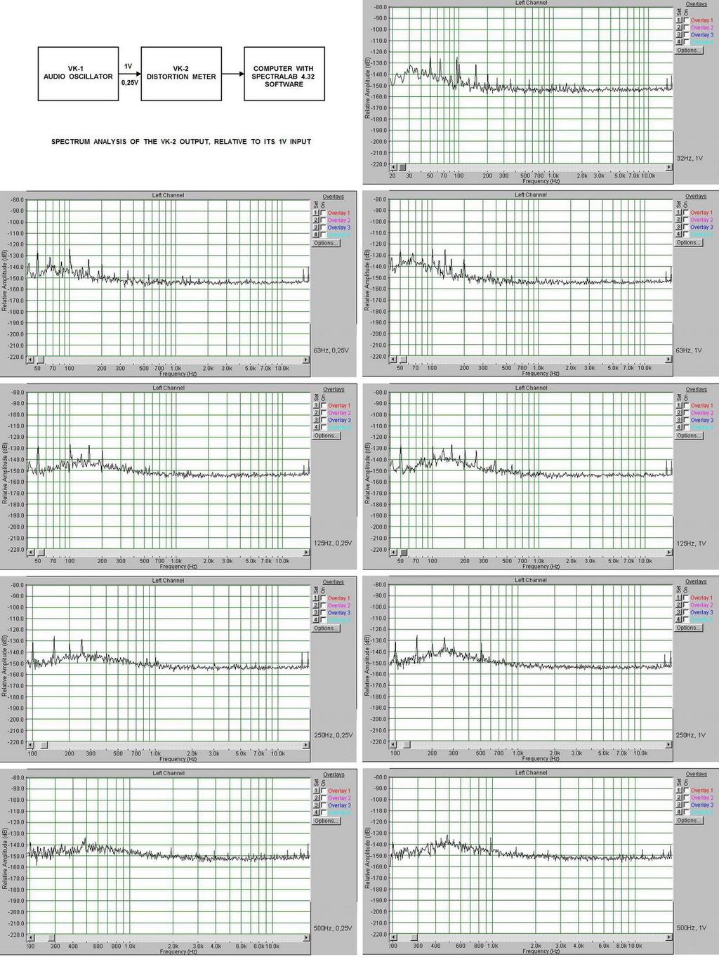
13 13
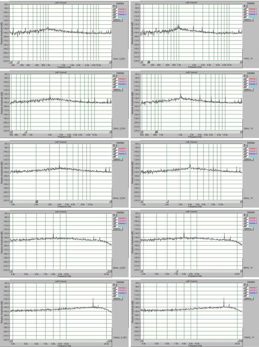
14 14
 for measurement bandwidth of 100kHz (0,00041%")

15 Fig.13. Distortion plot of the VK-1 oscillator + VK-2 distortion meter combination: 1 THD+Noise (%) for measurement bandwidth of 100kHz (0,00041% at 1kHz); 2 only Noise (%) for measurement bandwidth of 100kHz (0,00040% at 1kHz). The VK-1 oscillator and VK-2 distortion meter were designed and built more than ten years ago and since then these real instruments have been employed in numerous real measurements both when self-checking each other and when designing and testing various audio equipment. Fig.14. Simulation of the VK-1 oscillator circuitry. 15
16 I'm very scrupulous about my electronics designs and consider them uncompleted and not suitable for public disclosure until their circuitry operation is successfully simulated by such a trustworthy program as Multisim 10. The last two years I've carried out strict and comprehensive virtual testing of the whole VK-1 oscillator and its separate parts, all that has convinced me in remarkable properties of the Multisim 10 software and confirmed the validity of the oscillator design and impeccability of its operation. Here I would like to represent a fragment of the simulated circuitry, the virtual oscilloscope screen shows the oscillator main output (orange trace), the synchronous detector output (green trace) and the process of settling the output amplitude (see Fig.14). The measurement probes placed at some points of the circuit monitor the simulation process at these points and give detailed time-varying information about its main parameters (voltage, current, frequency). The virtual distortion analyzer reads <-100dB THD, the -100dB being a minimum limit of this interactive distortion measurement. The Multisim function of distortion analysis allows to evaluate distortion down to -160dB at once in the whole audio frequency range, but in our case it can be used only by opening the oscillating loop and testing the oscillator as a three-stage amplifier fed from the program s ideal 2V RMS sine-wave source. The modified for that oscillator circuit is shown in Fig.15. Fig.15. Simulation circuit for the Multisim distortion analysis. The obtained are the second and the third harmonics of distortion at the outputs of each stage within 20Hz-20kHz. The generated by the Multisim 10 simulation graphs are presented in Fig.16,17. 16
 separately from distortion contributed by the elements of amplitude")
17 Fig.16,17. Distortion analysis results. The aim of this virtual testing was to check the linearity of the VK-1 oscillating circuitry (its three discrete amplifying stages) separately from distortion contributed by the elements of amplitude stabilization (optocoupler and FET). Normally, the oscillator s two outputs are taken from its first and third stages, each loaded by a 680Ω potentiometer. Here the stages total loads are set correspondingly about 300Ω and 600Ω, the applied to them output voltages are 2V RMS. The obtained vanishingly small distortion figures can be confirmed in reality only by a precision spectrum analysis, and I am happy that the results of all latest virtual measurements match the results of the same measurements performed earlier with the help of real instruments. Fig.18. Front view of the VK-1 oscillator + VK-2 distortion meter set. 17

18 In conclusion, some words about the oscillator construction which adds to its outstanding characteristics two very important features the instrument s portability and convenience of its use. The front view of the VK-1 oscillator and VK-2 distortion meter is shown in Fig.18, dimensions of each instrument are mm, so both of them can be easily placed inside a briefcase and transported just to where you need to perform the test. The front panels aren t overloaded with controls, handling of these controls is simple and understandable, the number of manipulations with them is minimized when making basic audio measurements. The interior view of both instruments is represented in Fig.19. Constructions of the oscillator and distortion meter are very compact, that has required great care in making their printed circuit boards, placing components on them and finally mounting all parts of each instrument inside the case. In the oscillator, the two-inch neighborhood of its mains transformer and the lower board containing the oscillation loop doesn t negatively affect the output sinusoid characteristics. Fig.19. Interior view of the VK-1 oscillator + VK-2 distortion meter set. The oscillator configuration has excellent immunity from picking up interferences and hum, but decisive is of cause the used screening of the lower board and the components mounted around the control switches. The photo of Fig.15 shows the instruments in their exposed state being convenient for troubleshooting the screens are removed and the upper boards are unscrewed, turned 180º outwards and fixed on the rear panels, giving easy access to any element within the devices. The upper boards don t require screen protection at all. Mandatory conditions for successful operation of the oscillator are also the right grounding and the right, optimal connections between all its parts, particularly those delivering the power supply voltages. These bipolar ±15V voltages are produced by a stabilizer built on discrete components. I don t enclose the lists of components each instrument consists of, because here I don t offer a DIY (do it yourself) project. I simply would like to share all information that concerns this type of audio oscillator its theoretical background, practical realization on the example of the VK-1 instrument and, at last, minimizing and measuring distortion. There is no still commercial version of the VK-1 audio oscillator, but I hope it might appear in the near future. Copyright Vladimir Katkov, September
AUDIO OSCILLATOR DISTORTION
 AUDIO OSCILLATOR DISTORTION Being an ardent supporter of the shunt negative feedback in audio and electronics, I would like again to demonstrate its advantages, this time on the example of the offered
DISCRETE DIFFERENTIAL AMPLIFIER
 DISCRETE DIFFERENTIAL AMPLIFIER This differential amplifier was specially designed for use in my VK-1 audio oscillator and VK-2 distortion meter where the requirements of ultra-low distortion and ultra-low
AUDIO INVERTING AMPLIFIER
 AUDIO INVERTING AMPLIFIER The first sketches of this circuit appeared about twenty years ago when I started to develop an all-discrete audio preamplifier. I had a good example of building such things -
Operational Amplifiers
 Operational Amplifiers Table of contents 1. Design 1.1. The Differential Amplifier 1.2. Level Shifter 1.3. Power Amplifier 2. Characteristics 3. The Opamp without NFB 4. Linear Amplifiers 4.1. The Non-Inverting
LM13600 Dual Operational Transconductance Amplifiers with Linearizing Diodes and Buffers
 LM13600 Dual Operational Transconductance Amplifiers with Linearizing Diodes and Buffers General Description The LM13600 series consists of two current controlled transconductance amplifiers each with
Testing Power Sources for Stability
 Keywords Venable, frequency response analyzer, oscillator, power source, stability testing, feedback loop, error amplifier compensation, impedance, output voltage, transfer function, gain crossover, bode
LINEAR IC APPLICATIONS
 1 B.Tech III Year I Semester (R09) Regular & Supplementary Examinations December/January 2013/14 1 (a) Why is R e in an emitter-coupled differential amplifier replaced by a constant current source? (b)
Testing and Stabilizing Feedback Loops in Today s Power Supplies
 Keywords Venable, frequency response analyzer, impedance, injection transformer, oscillator, feedback loop, Bode Plot, power supply design, open loop transfer function, voltage loop gain, error amplifier,
Oscillators. An oscillator may be described as a source of alternating voltage. It is different than amplifier.
 Oscillators An oscillator may be described as a source of alternating voltage. It is different than amplifier. An amplifier delivers an output signal whose waveform corresponds to the input signal but
Op Amp Booster Designs
 Op Amp Booster Designs Although modern integrated circuit operational amplifiers ease linear circuit design, IC processing limits amplifier output power. Many applications, however, require substantially
Single Supply, Rail to Rail Low Power FET-Input Op Amp AD820
 a FEATURES True Single Supply Operation Output Swings Rail-to-Rail Input Voltage Range Extends Below Ground Single Supply Capability from + V to + V Dual Supply Capability from. V to 8 V Excellent Load
Physics 303 Fall Module 4: The Operational Amplifier
 Module 4: The Operational Amplifier Operational Amplifiers: General Introduction In the laboratory, analog signals (that is to say continuously variable, not discrete signals) often require amplification.
LF353 Wide Bandwidth Dual JFET Input Operational Amplifier
 LF353 Wide Bandwidth Dual JFET Input Operational Amplifier General Description These devices are low cost, high speed, dual JFET input operational amplifiers with an internally trimmed input offset voltage
Summer 2015 Examination
 Summer 2015 Examination Subject Code: 17445 Model Answer Important Instructions to examiners: 1) The answers should be examined by key words and not as word-to-word as given in the model answer scheme.
OBSOLETE. High Performance, BiFET Operational Amplifiers AD542/AD544/AD547 REV. B
 a FEATURES Ultralow Drift: 1 V/ C (AD547L) Low Offset Voltage: 0.25 mv (AD547L) Low Input Bias Currents: 25 pa max Low Quiescent Current: 1.5 ma Low Noise: 2 V p-p High Open Loop Gain: 110 db High Slew
Application Note AN45
 Application Note Wien Bridge Oscillators using E 2 POTs by Applications Staff, October 1994 Wien Bridge Oscillators In 1939, William R. Hewlett (later of Hewlett-Packard fame) first combined the network
Basic Electronics Learning by doing Prof. T.S. Natarajan Department of Physics Indian Institute of Technology, Madras
 Basic Electronics Learning by doing Prof. T.S. Natarajan Department of Physics Indian Institute of Technology, Madras Lecture 26 Mathematical operations Hello everybody! In our series of lectures on basic
TL082 Wide Bandwidth Dual JFET Input Operational Amplifier
 TL082 Wide Bandwidth Dual JFET Input Operational Amplifier General Description These devices are low cost, high speed, dual JFET input operational amplifiers with an internally trimmed input offset voltage
LM13700 Dual Operational Transconductance Amplifiers with Linearizing Diodes and Buffers
 LM13700 Dual Operational Transconductance Amplifiers with Linearizing Diodes and Buffers General Description The LM13700 series consists of two current controlled transconductance amplifiers, each with
Field Effect Transistors
 Field Effect Transistors Purpose In this experiment we introduce field effect transistors (FETs). We will measure the output characteristics of a FET, and then construct a common-source amplifier stage,
LF442 Dual Low Power JFET Input Operational Amplifier
 LF442 Dual Low Power JFET Input Operational Amplifier General Description The LF442 dual low power operational amplifiers provide many of the same AC characteristics as the industry standard LM1458 while
AN174 Applications for compandors SA570/571 SA571
 RF COMMUNICATIONS PRODUCTS Applications for compandors SA570/571 SA571 1997 Aug 20 Philips Semiconductors APPLICATIONS The following circuits will illustrate some of the wide variety of applications for
UNIT 2. Q.1) Describe the functioning of standard signal generator. Ans. Electronic Measurements & Instrumentation
 Describe the functioning of standard signal generator. Ans. Electronic Measurements & Instrumentation") UNIT 2 Q.1) Describe the functioning of standard signal generator Ans. STANDARD SIGNAL GENERATOR A standard signal generator produces known and controllable voltages. It is used as power source for the
UNIT 2 Q.1) Describe the functioning of standard signal generator Ans. STANDARD SIGNAL GENERATOR A standard signal generator produces known and controllable voltages. It is used as power source for the
Active Filter Design Techniques
 Active Filter Design Techniques 16.1 Introduction What is a filter? A filter is a device that passes electric signals at certain frequencies or frequency ranges while preventing the passage of others.
Chapter 5. Operational Amplifiers and Source Followers. 5.1 Operational Amplifier
 Chapter 5 Operational Amplifiers and Source Followers 5.1 Operational Amplifier In single ended operation the output is measured with respect to a fixed potential, usually ground, whereas in double-ended
EMT212 Analog Electronic II. Chapter 4. Oscillator
 EMT Analog Electronic II Chapter 4 Oscillator Objectives Describe the basic concept of an oscillator Discuss the basic principles of operation of an oscillator Analyze the operation of RC, LC and crystal
Audio Applications of Linear Integrated Circuits
 Audio Applications of Linear Integrated Circuits Although operational amplifiers and other linear ICs have been applied as audio amplifiers relatively little documentation has appeared for other audio
Oscillator Principles
 Oscillators Introduction Oscillators are circuits that generates a repetitive waveform of fixed amplitude and frequency without any external input signal. The function of an oscillator is to generate alternating
55:041 Electronic Circuits The University of Iowa Fall Exam 3. Question 1 Unless stated otherwise, each question below is 1 point.
 Exam 3 Name: Score /65 Question 1 Unless stated otherwise, each question below is 1 point. 1. An engineer designs a class-ab amplifier to deliver 2 W (sinusoidal) signal power to an resistive load. Ignoring
11. Chapter: Amplitude stabilization of the harmonic oscillator
 Punčochář, Mohylová: TELO, Chapter 10 1 11. Chapter: Amplitude stabilization of the harmonic oscillator Time of study: 3 hours Goals: the student should be able to define basic principles of oscillator
PHYS 536 The Golden Rules of Op Amps. Characteristics of an Ideal Op Amp
 PHYS 536 The Golden Rules of Op Amps Introduction The purpose of this experiment is to illustrate the golden rules of negative feedback for a variety of circuits. These concepts permit you to create and
LM4562 Dual High Performance, High Fidelity Audio Operational Amplifier
 Dual High Performance, High Fidelity Audio Operational Amplifier General Description The is part of the ultra-low distortion, low noise, high slew rate operational amplifier series optimized and fully
The steeper the phase shift as a function of frequency φ(ω) the more stable the frequency of oscillation
 the more stable the frequency of oscillation") It should be noted that the frequency of oscillation ω o is determined by the phase characteristics of the feedback loop. the loop oscillates at the frequency for which the phase is zero The steeper the
It should be noted that the frequency of oscillation ω o is determined by the phase characteristics of the feedback loop. the loop oscillates at the frequency for which the phase is zero The steeper the
OBSOLETE. Self-Contained Audio Preamplifier SSM2017 REV. B
 a FEATURES Excellent Noise Performance: 950 pv/ Hz or 1.5 db Noise Figure Ultralow THD: < 0.01% @ G = 100 Over the Full Audio Band Wide Bandwidth: 1 MHz @ G = 100 High Slew Rate: 17 V/ s typ Unity Gain
INTEGRATED CIRCUITS. AN109 Microprocessor-compatible DACs Dec
 INTEGRATED CIRCUITS 1988 Dec DAC products are designed to convert a digital code to an analog signal. Since a common source of digital signals is the data bus of a microprocessor, DAC circuits that are
Chapter 13 Oscillators and Data Converters
 Chapter 13 Oscillators and Data Converters 13.1 General Considerations 13.2 Ring Oscillators 13.3 LC Oscillators 13.4 Phase Shift Oscillator 13.5 Wien-Bridge Oscillator 13.6 Crystal Oscillators 13.7 Chapter
Single Supply, Rail to Rail Low Power FET-Input Op Amp AD820
 a FEATURES True Single Supply Operation Output Swings Rail-to-Rail Input Voltage Range Extends Below Ground Single Supply Capability from V to V Dual Supply Capability from. V to 8 V Excellent Load Drive
LM13700 Dual Operational Transconductance Amplifiers with Linearizing Diodes and Buffers
 LM13700 Dual Operational Transconductance Amplifiers with Linearizing Diodes and Buffers General Description The LM13700 series consists of two current controlled transconductance amplifiers, each with
LF411 Low Offset, Low Drift JFET Input Operational Amplifier
 Low Offset, Low Drift JFET Input Operational Amplifier General Description These devices are low cost, high speed, JFET input operational amplifiers with very low input offset voltage and guaranteed input
TL082 Wide Bandwidth Dual JFET Input Operational Amplifier
 TL082 Wide Bandwidth Dual JFET Input Operational Amplifier General Description These devices are low cost, high speed, dual JFET input operational amplifiers with an internally trimmed input offset voltage
Difference between BJTs and FETs. Junction Field Effect Transistors (JFET)
") Difference between BJTs and FETs Transistors can be categorized according to their structure, and two of the more commonly known transistor structures, are the BJT and FET. The comparison between BJTs
Difference between BJTs and FETs Transistors can be categorized according to their structure, and two of the more commonly known transistor structures, are the BJT and FET. The comparison between BJTs
LM148/LM248/LM348 Quad 741 Op Amps
 Quad 741 Op Amps General Description The LM148 series is a true quad 741. It consists of four independent, high gain, internally compensated, low power operational amplifiers which have been designed to
Practical Testing Techniques For Modern Control Loops
 VENABLE TECHNICAL PAPER # 16 Practical Testing Techniques For Modern Control Loops Abstract: New power supply designs are becoming harder to measure for gain margin and phase margin. This measurement is
EE 233 Circuit Theory Lab 2: Amplifiers
 EE 233 Circuit Theory Lab 2: Amplifiers Table of Contents 1 Introduction... 1 2 Precautions... 1 3 Prelab Exercises... 2 3.1 LM348N Op-amp Parameters... 2 3.2 Voltage Follower Circuit Analysis... 2 3.2.1
IC Preamplifier Challenges Choppers on Drift
 IC Preamplifier Challenges Choppers on Drift Since the introduction of monolithic IC amplifiers there has been a continual improvement in DC accuracy. Bias currents have been decreased by 5 orders of magnitude
LM6118/LM6218 Fast Settling Dual Operational Amplifiers
 Fast Settling Dual Operational Amplifiers General Description The LM6118/LM6218 are monolithic fast-settling unity-gain-compensated dual operational amplifiers with ±20 ma output drive capability. The
KH103 Fast Settling, High Current Wideband Op Amp
 KH103 Fast Settling, High Current Wideband Op Amp Features 80MHz full-power bandwidth (20V pp, 100Ω) 200mA output current 0.4% settling in 10ns 6000V/µs slew rate 4ns rise and fall times (20V) Direct replacement
EUA6210 Output Capacitor-less 67mW Stereo Headphone Amplifier
 Output Capacitor-less 67mW Stereo Headphone Amplifier DESCRIPTION The is an audio power amplifier primarily designed for headphone applications in portable device applications. It is capable of delivering
LF444 Quad Low Power JFET Input Operational Amplifier
 LF444 Quad Low Power JFET Input Operational Amplifier General Description The LF444 quad low power operational amplifier provides many of the same AC characteristics as the industry standard LM148 while
CHAPTER 3. Instrumentation Amplifier (IA) Background. 3.1 Introduction. 3.2 Instrumentation Amplifier Architecture and Configurations
 Background. 3.1 Introduction. 3.2 Instrumentation Amplifier Architecture and Configurations") CHAPTER 3 Instrumentation Amplifier (IA) Background 3.1 Introduction The IAs are key circuits in many sensor readout systems where, there is a need to amplify small differential signals in the presence
CHAPTER 3 Instrumentation Amplifier (IA) Background 3.1 Introduction The IAs are key circuits in many sensor readout systems where, there is a need to amplify small differential signals in the presence
Applied Electronics II
 Applied Electronics II Chapter 3: Operational Amplifier Part 1- Op Amp Basics School of Electrical and Computer Engineering Addis Ababa Institute of Technology Addis Ababa University Daniel D./Getachew
ELC224 Final Review (12/10/2009) Name:
 Name:") ELC224 Final Review (12/10/2009) Name: Select the correct answer to the problems 1 through 20. 1. A common-emitter amplifier that uses direct coupling is an example of a dc amplifier. 2. The frequency
ELC224 Final Review (12/10/2009) Name: Select the correct answer to the problems 1 through 20. 1. A common-emitter amplifier that uses direct coupling is an example of a dc amplifier. 2. The frequency
Integrated Circuit: Classification:
 Integrated Circuit: It is a miniature, low cost electronic circuit consisting of active and passive components that are irreparably joined together on a single crystal chip of silicon. Classification:
WESTREX RA-1712 PHOTOGRAPHIC SOUND RECORD ELECTRONICS
 INTRODUCTION The RA-1712 solid state Record Electronics is an integrated system for recording photographic sound tracks on a Westrex photographic sound recorder. It accepts a 600Ω input signal level from
Operational Amplifier BME 360 Lecture Notes Ying Sun
 Operational Amplifier BME 360 Lecture Notes Ying Sun Characteristics of Op-Amp An operational amplifier (op-amp) is an analog integrated circuit that consists of several stages of transistor amplification
ECE3204 D2015 Lab 1. See suggested breadboard configuration on following page!
 ECE3204 D2015 Lab 1 The Operational Amplifier: Inverting and Non-inverting Gain Configurations Gain-Bandwidth Product Relationship Frequency Response Limitation Transfer Function Measurement DC Errors
A Simplified Test Set for Op Amp Characterization
 A Simplified Test Set for Op Amp Characterization INTRODUCTION The test set described in this paper allows complete quantitative characterization of all dc operational amplifier parameters quickly and
DEPARTMENT OF ELECTRICAL ENGINEERING AND COMPUTER SCIENCE MASSACHUSETTS INSTITUTE OF TECHNOLOGY CAMBRIDGE, MASSACHUSETTS 02139
 DEPARTMENT OF ELECTRICAL ENGINEERING AND COMPUTER SCIENCE MASSACHUSETTS INSTITUTE OF TECHNOLOGY CAMBRIDGE, MASSACHUSETTS 019.101 Introductory Analog Electronics Laboratory Laboratory No. READING ASSIGNMENT
Input Stage Concerns. APPLICATION NOTE 656 Design Trade-Offs for Single-Supply Op Amps
 Maxim/Dallas > App Notes > AMPLIFIER AND COMPARATOR CIRCUITS Keywords: single-supply, op amps, amplifiers, design, trade-offs, operational amplifiers Apr 03, 2000 APPLICATION NOTE 656 Design Trade-Offs
Laboratory 8 Operational Amplifiers and Analog Computers
 Laboratory 8 Operational Amplifiers and Analog Computers Introduction Laboratory 8 page 1 of 6 Parts List LM324 dual op amp Various resistors and caps Pushbutton switch (SPST, NO) In this lab, you will
Chapter 8. Field Effect Transistor
 Chapter 8. Field Effect Transistor Field Effect Transistor: The field effect transistor is a semiconductor device, which depends for its operation on the control of current by an electric field. There
Using LME49810 to Build a High-Performance Power Amplifier Part I
 Using LME49810 to Build a High-Performance Power Amplifier Part I Panson Poon Introduction Although switching or Class-D amplifiers are gaining acceptance to audiophile community, linear amplification
New Technique Accurately Measures Low-Frequency Distortion To <-130 dbc Levels by Xavier Ramus, Applications Engineer, Texas Instruments Incorporated
 New Technique Accurately Measures Low-Frequency Distortion To
Applications of the LM392 Comparator Op Amp IC
 Applications of the LM392 Comparator Op Amp IC The LM339 quad comparator and the LM324 op amp are among the most widely used linear ICs today. The combination of low cost, single or dual supply operation
LF155/LF156/LF355/LF356/LF357 JFET Input Operational Amplifiers
 JFET Input Operational Amplifiers General Description These are the first monolithic JFET input operational amplifiers to incorporate well matched, high voltage JFETs on the same chip with standard bipolar
A 7ns, 6mA, Single-Supply Comparator Fabricated on Linear s 6GHz Complementary Bipolar Process
 A 7ns, 6mA, Single-Supply Comparator Fabricated on Linear s 6GHz Complementary Bipolar Process Introduction The is an ultrafast (7ns), low power (6mA), single-supply comparator designed to operate on either
UNIT-3. Electronic Measurements & Instrumentation
 UNIT-3 1. Draw the Block Schematic of AF Wave analyzer and explain its principle and Working? ANS: The wave analyzer consists of a very narrow pass-band filter section which can Be tuned to a particular
Homework Assignment 03
 Homework Assignment 03 Question 1 (Short Takes), 2 points each unless otherwise noted. 1. Two 0.68 μf capacitors are connected in series across a 10 khz sine wave signal source. The total capacitive reactance
Analysis and Design of a Simple Operational Amplifier
 by Kenneth A. Kuhn December 26, 2004, rev. Jan. 1, 2009 Introduction The purpose of this article is to introduce the student to the internal circuits of an operational amplifier by studying the analysis
EUA2011A. Low EMI, Ultra-Low Distortion, 2.5-W Mono Filterless Class-D Audio Power Amplifier DESCRIPTION FEATURES APPLICATIONS
 Low EMI, Ultra-Low Distortion, 2.5-W Mono Filterless Class-D Audio Power Amplifier DESCRIPTION The EUA2011A is a high efficiency, 2.5W mono class-d audio power amplifier. A new developed filterless PWM
New Techniques for Testing Power Factor Correction Circuits
 Keywords Venable, frequency response analyzer, impedance, injection transformer, oscillator, feedback loop, Bode Plot, power supply design, power factor correction circuits, current mode control, gain
Wien-Bridge oscillator has simplified frequency control
 Wien-Bridge oscillator has simplified frequency control High-quality audio signal generators mae extensive use of the Wien-Bridge oscillator as a basic building bloc. The number of frequency decades covered
Programmable analog compandor
 DESCRIPTION The NE572 is a dual-channel, high-performance gain control circuit in which either channel may be used for dynamic range compression or expansion. Each channel has a full-wave rectifier to
LIMITATIONS IN MAKING AUDIO BANDWIDTH MEASUREMENTS IN THE PRESENCE OF SIGNIFICANT OUT-OF-BAND NOISE
 LIMITATIONS IN MAKING AUDIO BANDWIDTH MEASUREMENTS IN THE PRESENCE OF SIGNIFICANT OUT-OF-BAND NOISE Bruce E. Hofer AUDIO PRECISION, INC. August 2005 Introduction There once was a time (before the 1980s)
Chapter 2 Signal Conditioning, Propagation, and Conversion
 09/0 PHY 4330 Instrumentation I Chapter Signal Conditioning, Propagation, and Conversion. Amplification (Review of Op-amps) Reference: D. A. Bell, Operational Amplifiers Applications, Troubleshooting,
Electric Circuit Theory
 Electric Circuit Theory Nam Ki Min nkmin@korea.ac.kr 010-9419-2320 Chapter 15 Active Filter Circuits Nam Ki Min nkmin@korea.ac.kr 010-9419-2320 Contents and Objectives 3 Chapter Contents 15.1 First-Order
9 Feedback and Control
 9 Feedback and Control Due date: Tuesday, October 20 (midnight) Reading: none An important application of analog electronics, particularly in physics research, is the servomechanical control system. Here
Model 4402B. Ultra-Pure Sinewave Oscillator 1Hz to 110kHz Typical Distortion of % Serial No. Operating Manual
 Model 4402B Ultra-Pure Sinewave Oscillator 1Hz to 110kHz Typical Distortion of 0.0005% Serial No. Operating Manual 15 Jonathan Drive, Unit 4, Brockton, MA 02301 U.S.A. Tel: (508) 580-1660; Fax: (508) 583-8989
Homework Assignment 07
 Homework Assignment 07 Question 1 (Short Takes). 2 points each unless otherwise noted. 1. A single-pole op-amp has an open-loop low-frequency gain of A = 10 5 and an open loop, 3-dB frequency of 4 Hz.
Constant Current Control for DC-DC Converters
 Constant Current Control for DC-DC Converters Introduction...1 Theory of Operation...1 Power Limitations...1 Voltage Loop Stability...2 Current Loop Compensation...3 Current Control Example...5 Battery
OBSOLETE. Parameter AD9621 AD9622 AD9623 AD9624 Units
 a FEATURES MHz Small Signal Bandwidth MHz Large Signal BW ( V p-p) High Slew Rate: V/ s Low Distortion: db @ MHz Fast Settling: ns to.%. nv/ Hz Spectral Noise Density V Supply Operation Wideband Voltage
Low Pass Filter Introduction
 Low Pass Filter Introduction Basically, an electrical filter is a circuit that can be designed to modify, reshape or reject all unwanted frequencies of an electrical signal and accept or pass only those
 Distributed by: www.jameco.com 1-800-831-4242 The content and copyrights of the attached material are the property of its owner. LM148/LM248/LM348 Quad 741 Op Amps General Description The LM148 series
UNIVERSITI MALAYSIA PERLIS
 UNIVERSITI MALAYSIA PERLIS ANALOG ELECTRONICS II EMT 212 2009/2010 EXPERIMENT # 3 OP-AMP (OSCILLATORS) 1 1. OBJECTIVE: 1.1 To demonstrate the Wien bridge oscillator 1.2 To demonstrate the RC phase-shift
EXPERIMENT 2.2 NON-LINEAR OP-AMP CIRCUITS
 2.16 EXPERIMENT 2.2 NONLINEAR OPAMP CIRCUITS 2.2.1 OBJECTIVE a. To study the operation of 741 opamp as comparator. b. To study the operation of active diode circuits (precisions circuits) using opamps,
EE301 Electronics I , Fall
 EE301 Electronics I 2018-2019, Fall 1. Introduction to Microelectronics (1 Week/3 Hrs.) Introduction, Historical Background, Basic Consepts 2. Rewiev of Semiconductors (1 Week/3 Hrs.) Semiconductor materials
Capacitive Touch Sensing Tone Generator. Corey Cleveland and Eric Ponce
 Capacitive Touch Sensing Tone Generator Corey Cleveland and Eric Ponce Table of Contents Introduction Capacitive Sensing Overview Reference Oscillator Capacitive Grid Phase Detector Signal Transformer
Chapter 13: Introduction to Switched- Capacitor Circuits
 Chapter 13: Introduction to Switched- Capacitor Circuits 13.1 General Considerations 13.2 Sampling Switches 13.3 Switched-Capacitor Amplifiers 13.4 Switched-Capacitor Integrator 13.5 Switched-Capacitor
Test Your Understanding
 074 Part 2 Analog Electronics EXEISE POBLEM Ex 5.3: For the switched-capacitor circuit in Figure 5.3b), the parameters are: = 30 pf, 2 = 5pF, and F = 2 pf. The clock frequency is 00 khz. Determine the
QUAD 5V RAIL-TO-RAIL PRECISION OPERATIONAL AMPLIFIER
 ADVANCED LINEAR DEVICES, INC. ALD472A/ALD472B ALD472 QUAD 5V RAILTORAIL PRECISION OPERATIONAL AMPLIFIER GENERAL DESCRIPTION The ALD472 is a quad monolithic precision CMOS railtorail operational amplifier
Homework Assignment 06
 Question 1 (2 points each unless noted otherwise) Homework Assignment 06 1. True or false: when transforming a circuit s diagram to a diagram of its small-signal model, we replace dc constant current sources
Dual FET-Input, Low Distortion OPERATIONAL AMPLIFIER
 www.burr-brown.com/databook/.html Dual FET-Input, Low Distortion OPERATIONAL AMPLIFIER FEATURES LOW DISTORTION:.3% at khz LOW NOISE: nv/ Hz HIGH SLEW RATE: 25V/µs WIDE GAIN-BANDWIDTH: MHz UNITY-GAIN STABLE
LME49710 High Performance, High Fidelity Audio Operational Amplifier
 High Performance, High Fidelity Audio Operational Amplifier General Description The LME49710 is part of the ultra-low distortion, low noise, high slew rate operational amplifier series optimized and fully
When input, output and feedback voltages are all symmetric bipolar signals with respect to ground, no biasing is required.
 1 When input, output and feedback voltages are all symmetric bipolar signals with respect to ground, no biasing is required. More frequently, one of the items in this slide will be the case and biasing
DUAL ULTRA MICROPOWER RAIL-TO-RAIL CMOS OPERATIONAL AMPLIFIER
 ADVANCED LINEAR DEVICES, INC. ALD276A/ALD276B ALD276 DUAL ULTRA MICROPOWER RAILTORAIL CMOS OPERATIONAL AMPLIFIER GENERAL DESCRIPTION The ALD276 is a dual monolithic CMOS micropower high slewrate operational
CHAPTER 2 A SERIES PARALLEL RESONANT CONVERTER WITH OPEN LOOP CONTROL
 14 CHAPTER 2 A SERIES PARALLEL RESONANT CONVERTER WITH OPEN LOOP CONTROL 2.1 INTRODUCTION Power electronics devices have many advantages over the traditional power devices in many aspects such as converting
A 24 V Chopper Offset-Stabilized Operational Amplifier with Symmetrical RC Notch Filters having sub-10 µv offset and over-120db CMRR
 ROMANIAN JOURNAL OF INFORMATION SCIENCE AND TECHNOLOGY Volume 20, Number 4, 2017, 301 312 A 24 V Chopper Offset-Stabilized Operational Amplifier with Symmetrical RC Notch Filters having sub-10 µv offset
Specify Gain and Phase Margins on All Your Loops
 Keywords Venable, frequency response analyzer, power supply, gain and phase margins, feedback loop, open-loop gain, output capacitance, stability margins, oscillator, power electronics circuits, voltmeter,
Testing Power Factor Correction Circuits For Stability
 Keywords Venable, frequency response analyzer, impedance, injection transformer, oscillator, feedback loop, Bode Plot, power supply design, switching power supply, PFC, boost converter, flyback converter,
Homework Assignment 13
 Question 1 Short Takes 2 points each. Homework Assignment 13 1. Classify the type of feedback uses in the circuit below (i.e., shunt-shunt, series-shunt, ) Answer: Series-shunt. 2. True or false: an engineer