1.09 GHz Mode-S Receiver Design and VHF Radar Antenna Characterization
|
|
|
- Preston Baldwin
- 6 years ago
- Views:
Transcription
1 1.09 GHz Mode-S Receiver Design and VHF Radar Antenna Characterization By Dabin Zhang Senior Thesis in Electrical Engineering University of Illinois at Urbana-Champaign Advisor: Professor Steven J. Franke May 2013
2 Abstract The design and implementation of a 1.09 GHz tuned-radio-frequency (TRF) receiver which can capture mode-s secondary surveillance radar reply frames sent by aircraft transponders is discussed in this thesis. The RF frontend of the receiver employs an RF-IC and SAW filter and detects the envelope of the input signal. The detected envelope signal is sampled and demodulated by FPGA firmware to reconstruct mode-s frames which can be retrieved via a Universal Serial Bus (USB) interface. Mode-S frame recording and decoding programs were written in C++ to extract aircraft information such as latitude, longitude, altitude, and aircraft identification number. Some decoded data has been combined with radar backscatter data collected by a VHF remote sensing radar to characterize the radiation pattern of the radar antenna arrays. The analyses confirmed that one antenna array performs according to theoretical expectation and uncovered a significant problem with another antenna array due to a coaxial cable connectivity issue. Subject Keywords: tuned radio frequency receiver, mode-s, ADS-B, antenna pattern measurement ii
3 Contents 1. Introduction... 1 Project Overview... 1 Transponder... 1 Mode-S... 2 ADS-B... 3 VHF radar Receiver Design... 8 Product Overview... 8 RF Design... 9 Digital Design Firmware Design System Design and Construction Receiver Testing Radar Antenna Characterization Overview Mode-S Data Processing ADS-B Data Selection Radar Data Extraction Evaluation Method Analyze Result Conclusions and Future Work iii
4 Appendix Circuit Schematics C++ Code for Data Collection C++ Code for Mode-S Decoding MATLAB Code for Data Analyze References iv

5 1. Introduction Project Overview This project consists of two parts. The first part is 1.09 GHz mode-s receiver design, where the receiver is designed to capture and demodulate mode-s downlink frames sent by aircraft transponders at 1.09 GHz. The second part of this project is VHF radar antenna characterization. The data captured by the mode-s receiver was decoded and position reports from particular aircraft have been combined with radar data to characterize the radiation pattern of the radar antenna array. Transponder A typical interrogation and reply cycle between ground radar station and aircraft is shown in Figure 1. The secondary radar interrogator transmits an interrogation frame (uplink) to the aircraft at 1.03 GHz and the aircraft transmits a reply frame (downlink) at 1.09 GHz after it receives the interrogation frame. Figure 2 is a typical transponder front panel. The LED screen shows current altitude is FL065 which is =6500 feet and squawk code is 1200 which is for visual flight rules (VFR) flight. Figure 1 Typical interrogation cycle. Adapted from [1] Both altitude and squawk will display on air traffic controllers (ATC) radar screen. The squawk code can be entered through keypad and mode can be selected through the knob. Transponders for civil aircraft have three different modes which are mode-a, mode-c and mode-s and most commercial transponders are capable of all those modes. Mode-A contains identification information 1 Figure 2 Front panel of KT-76C transponder. Adapted from [2]
 which is amplitude shift keying (ASK) with 13-bit length.")

6 which is squawk code and mode-c contains altitude code. Mode-S, however, can carry multiple types of data with larger package size. Mode-A and mode-c reply frames have the same format (Figure 3 [3]) which is amplitude shift keying (ASK) with 13-bit length. All mode-a/c downlink frames have a start pulse (F 1 ) and end pulse (F 2 ) which are on the front and end of data block. The SPI pulse at the end indicates the status of transponder. Figure 3 Mode A/C reply frame Mode-S Mode-S stands for mode select, because only a particular aircraft will respond to the radar interrogation since all aircraft are assigned a unique address code (ICAO address). This technique provides improved surveillance capability and using a discrete address permits information exchange between ground radar station and aircraft which forms a data link [4]. As can be seen in Figure 4, aircraft not only transmit data to ground air traffic controller (ATC) facility and other aircraft, but they also broadcast some data. Figure 4 Mode-S data link. Adapted from [5] Since the receiver discussed in this thesis is designed for the mode-s signal sent by aircraft transponders, 2
7 only the downlink data format is discussed. As shown in Figure 3 [3], each mode-s downlink frame contains a preamble and a data block. Pulse-position modulation (PPM) is used to send these frames on 1.09 GHz carrier. Figure 5 Mode S reply waveform As defined by the International Civil Aviation Organization (ICAO), the first five bits of a mode-s frame indicates its type (DF0 to DF31) [4]. Moreover, the first bit of the data block represents the length of the frame, bit1=0 (DF0 to DF15) stands for 56-bit data block and bit1=1 (DF16 to DF31) stands for 112-bit data block. Since the data rate of the mode-s downlink is 1Mbps, the total length of each frame is 64µs or 120µs. ADS-B ADS-B stands for automatic dependent surveillance-broadcast which is a new generation of surveillance technique that allows aircraft to broadcast their own information such as GPS coordinate, altitude, flight number and other information via mode-s frames. As defined in mode-s standards, ADS-B uses DF11 and DF17 type of mode-s frames to broadcast information. Such a broadcast is called a squitter. As shown in Figure 6 [6], DF11 frames do not contain any aircraft information other than 24-bit ICAO address and DF17 frames contain an extra 56-bit ADS-B data block. DF11 format Total 56-bit bit Capability 3-bit ICAO address 24-bit ----Parity bit DF17 format Total 112-bit bit Capability 3-bit ICAO address 24-bit ADS-B data 56-bit Parity 24-bit Figure 6 ADS-B frame structure 3
8 The first five bits of 56-bit ADS-B data block in DF17 frames contain a subtype code (0 to 31) which indicates the type of information encoded in the 56-bit data block. Table 1 [6] shows some typical subtypes and their usage. Table 1 ADS-B frame type Subtype Content 0 Barometric altitude or no altitude information, no position information 1 ~ 4 Aircraft identification and category message only 5 ~ 8 Surface position message only, type depends on horizontal containment radius limit 9 ~ 18 Airborne position message with barometric altitude 19 Airborne velocity message with difference between barometric altitude and GNSS Height 20 ~ 22 Airborne position message with GNSS Height (HAE) 23 ~ 31 Other Figure 7 [6] shows the structure of subtype 9 to bit ADS-B data block in DF17 frames, altitude and coordinate information are encoded. Subtype 5-bit Status 3-bit Altitude 12-bit Time flag 1-bit CPR flag 1-bit Latitude 17-bit Longitude 17-bit Figure 7 ADS-B airborne position frame s data block VHF radar The VHF radar is a 2-channel VHF remote sensing radar interferometer, whose hardware was designed by Professor Steven J. Franke and software was designed by Professor Erhan Kudeki. Both channels are receiving on 49.8 MHz, but only channel 1 is transmitting at the same frequency with 15 kw (PEP) transmitting power and 140 µs pulse width for each 4 ms cycle. The average output power is 525 W and duty cycle is 3.5%. The 140 µs pulse is binary phase-shift coded with a 28 baud code. The baud length is 5 µs which sets the range resolution of the radar to 750 m. The receiving system samples the signal every 2.5 µs, corresponding to range-sampling-interval of 375 m. 4
.")
9 Figure 8 Photo of VHF radar antenna array Each antenna array of the VHF radar is formed by four coaxial collinear antennas fed with different phase shift to create a narrow main beam directed toward the north. The main beam peaks at an elevation angle of approximately 17. There are two antenna arrays built for the radar and they are lined up in the east-west direction (Figure 8). Since this antenna array is too large to perform an anechoic chamber measurement and commercial aircrafts can be spotted by the radar, the antenna pattern is characterized by aircraft echoes. 5


10 Figure 9 A typical radar image This radar generates one MATLAB format output file containing the processed data for each ten minute period. Each output file contains two 600-second 2-dimensional radar images for each channel. As shown in Figure 9, x-axis of radar image stands for time, y-axis stands for distance between the radar antenna and aircraft and the color of each pixel on the image represents the corresponding reflection power. Most of the patterns in Figure 9 with distance smaller than 100 km are the aircraft echoes. Figure 10 is a zoomed-in view of one of the aircraft echoes in another radar file. The distance between aircraft and radar antenna is around 47 km. The vertical Figure 10 A typical aircraft echo pattern which shows up between 520 s and 570 s are range sidelobes from the 28 baud binary phase 6
11 code that modulates each radar pulse. Moreover, the main trace of the aircraft is not continuous because the aircraft is moving between antenna beams (main beam, first side lobe, second side lobe, etc.) and the radar can only detect reflection power when the aircraft is in one of those beams. 7


 since larger quantities will have lower component costs and")
12 2. Receiver Design Product Overview Figure 11 Top, bottom, and side view of receiver The physical dimension of the receiver is and it is implemented on a 4-layer PCB with through hole vias. The total development time of the receiver is two months with one person and $1000 funding. Average cost of each prototype receiver is $176 and the price will decrease dramatically if the quantity increases (Table 2, all prices in USD) since larger quantities will have lower component costs and automated PCB assembly techniques can be used. 8
13 Table 2 Quantity versus cost Quantity ICs Other Critical part Miscellaneous part PCB Assembly cost Total cost There are some similar products available commercially including mode-s beast, AVR receiver, SBS receiver and Table 3 shows the comparison in performance and price (USD). Table 3 Comparison of some existing mode-s receivers Model Price Structure Development Team Comment Mode-S Beast 1 Channel 380 ADC FPGA Multiple engineers High price Mode-S Beast 2 Channel 519 ADC FPGA Multiple engineers High price Transponder-Mouse 510 ADC FPGA Multiple engineers High price microadsb 95 Microcontroller Small commercial company Low performance Kinetic SBS ADC FPGA Commercial company High price As can be seen in Table 4, those products either have a high price with high performance or low price by using simple and low performance structure. Since both of them have a relative low performance/price ratio, the goal of this design is to create a receiver which has moderate price and high performance. RF Design Overview The RF part can be divided into two parts. The function of the first part is amplification and channel selection, which is accomplished with a combination of surface acoustic wave (SAW) band pass filters (BPF) and RF amplifiers. The function of the second part is envelope detection which extracts the envelope of the input RF signal, similar to an amplitude modulation (AM) demodulator. There are two kinds of SAW BPF available at 1.09 GHz with bandwidths of 30MHz and 12MHz. These are narrow enough for channel selection, so there is no need to implement an intermediate frequency (IF) stage for further channel selection. Thus this is a tuned radio frequency (TRF) receiver and only works at 1.09 GHz. 9
14 Since the distance between the receiver s antenna and the aircraft may vary from less than one kilometer to several hundred kilometers, the RF part requires both high sensitivity and high dynamic range. Moreover, the envelope signal of RF frontend is generated by a logarithmic detector which measures the overall input signal power, so the noise added by the amplification stages has to be minimized. Also, the overall power consumption has to be low because this receiver is designed to be powered from the USB bus which can provide maximum power P=5V 500mA=2.5 W. Component Selection To select the transponder s signal at 1.09 GHz, a proper filter has to be selected. There are four different filters available at this frequency and two of them, TA0232 and TA1090EC, were selected. TA1090EC is selected because it has wider bandwidth and lower insertion loss. TA0232 is selected because it has narrower bandwidth. Two low noise amplifiers (LNA), ADL5523 and MAX2640, were selected to provide low noise amplification for the RF front end. ADL5523 has relative higher gain and lower noise than the MAX2640, but it has higher power consumption. To provide sufficient gain for the envelope detector part, a general purpose gain block AD8354 was selected because it does not require complex external circuitry, such as matching a network, and it has high gain. There are multiple methods for demodulation but envelope detection method is the most convenient structure for this receiver. To ensure the performance and efficiency, a logarithmic detector is used instead of a Schottky diode and capacitor which used in AM demodulation. AD8313 is selected because it has moderate response time and power requirement. To connect the amplification part with TA0232 SAW BPF and envelope detector, a balanced to unbalanced converter (BALUN) is needed to convert unbalanced output signal into balanced. TC1-1-13M+ is selected for this purpose since it has low insertion loss and impedance transfer ratio is 1:1. 10
.")

15 Matching Network All the LNAs in this design must be properly matched to achieve highest performance at the design frequency. All the matching networks were implemented as L-networks. ADL5523 The ADL5523 requires an input matching network located at its input port and an output matching network located at the power port (pin8). Output (power) port matching is the first step to match the amplifier and input port matching can be determined when optimum S 22 is achieved. Since the output port matching is hard to characterize with common L-network matching model and example matching networks for some common frequencies were given by the datasheet, the matching network was first built for 0.9 GHz and then move to 1.09 GHz by Figure 12 Prototype for ADL5523 adjusting components values. The key element for output matching is L 6 (Figure 12). For prototype circuit (Figure 12), finished matching network gives gain G=15.24 db and noise figure NF=1.2 db with power consumption P=105 mw. Figure 13 Circuit schematic for ADL


.")
16 The finished circuit schematic for ADL5523 is shown in Figure 13, R 40, R 37, R 20, R 38 are reserved for further adjustment and not used for this design. MAX2640 The MAX2640 requires matching networks on its input and output ports. Since the matching network design of this amplifier can be modeled as a common matching network, the S-parameter of the amplifier at 1.09 GHz has been measured and the components value of L-network was calculated. Moreover, a recommended L-network design at 0.9 GHz was given in the datasheet and this example has been used as the starting point of matching network design. Figure 14 Prototype for MAX2640 By testing with different component, finished matching network gives gain G=14.05 db and noise figure NF=2.17 db on prototype board (Figure 14). Figure 15 Circuit schematic for MAX2640 AD8354 Since this amplifier is a general purpose gain block and internally matched to 50 Ω, no extra matching circuit was implemented. The finished prototype circuit (Figure 16) provides gain G=18.9 db and Figure 16 Prototype for AD8354 noise figure NF=4.2 db. 12

17 Final circuit schematic for AD8354 is shown in Figure 17. A 100 nh pull-up inductor L 2 was inserted between pin 6 (V CC ) and pin 7 (output) to increase gain. Figure 17 Circuit schematic for AD8354 Envelope Detector The core of envelope detector is AD8313, a GHz 70dB logarithmic detector which output is the logarithmic of PEP input power (envelope) and this detector can detect input power from around -65 dbm to 5 dbm. In this application, the output of logarithmic amplifier is sampled by an ADC for further Figure 18 Prototype for envelope detector processing. The alternative solution of envelope detection is to implement an intermediate frequency (IF) stage and use ADC to sample the IF or base band (BF) signal. Table 4 lists the comparison of those two configurations. Table 4 Comparison between envelope detector and IF stage Envelope Detector Implementation Intermediate Frequency Implementation Circuit Complexity Single Chip (AD8313) At least has mixer, LO, IF BPF Power Consumption 3.3V 7mA=23 mw >500 mw Sensitivity 12 MHz BPF reduce SNR by 3 Mixer bring in extra noise Cost Low High 13
18 Figure 18 shows a prototype version of the envelope detector, input signal has been converted to balanced and feed into TA0232 BPF before reach AD8313. Final circuit schematic for AD8313 is shown in Figure 19. To match 50 Ω source to the input impedance of AD8313, a matching network were designed (R 8, C 9 and C 10 ) and R 8 can be replaced by an inductor to reduce ohmic loss. Figure 19 Circuit schematic for AD8313 Component Arrangement Figure 20 Block diagram for RF frontend Since there may be strong interference sources in the receiver s working environment, a pre-selector is required to reject those unwanted components picked up by the antenna. However, insert a pre-selector between antenna and amplifier will not only bring in extra loss but can also increase the system noise dramatically. Thus TA1090EC was used for pre-selector because it has moderate insertion loss and 3 db 14
19 bandwidth. To ensure the low noise nature of the RF front end, LNAs must be placed immediately after the pre-selector. Since ADL5523 has the lowest noise and relatively high gain (lowest noise measure), it was used as the first amplifier. MAX2640 was used as the second amplifier because it has higher noise figure than ADL5523 but lower power consumption. Moreover, MAX2640 can keep its output power under the maximum rating of later stage when an excessive strong signal is fed into its input since the 1dB compression point is only -22 dbm. An extra filter was placed after MAX2640 to attenuate harmonics generated by intermodulation caused by strong signals due to the MAX2640 s relatively low input intercept level. Since the total gain of the first two amplifiers is only 29dB, a third amplifier AD8354 is used to provide extra gain. Table 5 Comparison of different amplifier and filter combinations # Circuit Configuration (same as signal flow) Noise Figure db Gain db Power mw 1 ADL5523 ADL5523 MAX ADL5523 ADL5523 AD ADL5523 MAX2640 AD MAX2640 MAX2640 AD MAX2640 AD8354 AD ADL5523 TA1090EC MAX2640 AD Table 5 Table 5lists different configuration for the amplification part with corresponding measured performance. The third configuration has the highest performance; therefore this combination was used for final design. The last stage of RF frontend is envelope detector AD8313. To enhance selectivity, TA0232 was placed before AD8313 to limit the equivalent noise bandwidth to 12 MHz and TC1-1-13M+ is placed between AD8354 and TA0232 to transfer the unbalanced transmission line into balanced. 15

 and U 14 (TA1090).")
20 Figure 21 is a photo of RF prototype board including the amplification part and envelope detector. The RF circuit is placed in a RF shield to prevent interference. The SMA socket on the left is antenna input, socket on the top is envelope signal video output and SMA connector on the bottom is an extra port reserved for RF testing. Final PCB Design Figure 21 Prototype for RF frontend Figure 22 Final layout of RF frontend As shown Figure 22, antenna output signal comes into the RF frontend through a SMA connector (J 11 ) via coplanar waveguide and envelope signal is fed into ADC. The envelope signal is also connected to the video test point located in the middle of U 18 (AD8313) and U 14 (TA1090). To have maximum isolation between different stages, the signal is guided in an S shaped structure. 16
21 Testing Unless noted, 3.3 V DC power for RF frontend is provided by Agilent E3648A power supply and testing frequency is 1.09 GHz. Amplifier-Filter Network Measurement The amplifier network can be treated as a two port network and it can be characterized through S-parameters, noise, and nonlinearity measurements. Since the finished PCB has a reserved RF test port between the last amplifier and BALUN, the test port is used as the output of amplification part. S-parameters and gain compression were measured using an Agilent E8357APNA with SOLT calibration standard (Agilent 85052D 3.5mm Economy Calibration Kit). Figure 23 RF frontend S-parameter and gain compression measurement At 1.09 GHz, measured S 21 = db, 1dB gain compression point P 1dB = dbm. 3 db bandwidth of the amplification stage is BW 3dB = MHz, 30 db bandwidth is BW 30dB = MHz and Shape Factor =
22 Noise is measured through Noise Figure function in Agilent N9020A MXA Signal Analyzer with Agilent N4001A series noise source. As shown in Figure 24, measured noise figure NF=2.0 db, gain G=44.4 db at 1.09 GHz. Figure 24 Noise measurement of RF frontend Power consumption was measured by the built-in ampere meter of the power supply when a single tone is fed into the input port of RF frontend. When input signal is lower than -40 dbm, total power consumption of RF frontend is P = 3.3V 75mA = mw. Maximum power consumption is lower than mw with -10 dbm input signal. Two-tone third-order input intercept (IIP3) was measured by the following setup: two different input tones were generated by two HP E4432B ESG-D series signal generators and combined by Mini-Circuit ZESC splitter before fed into the receiver. The output spectrum was measured through spectrum analyzer mode in Agilent N9020A MXA Signal Analyzer at receiver s RF testing port. Measurement shows the overall two-tone third-order input intercept (IIP3) is dbm 18
23 Figure 25 Two-tone third-order measurement Envelope Detector Measurement Since the envelope detector s output is the envelope (power) of the input signal, it can be characterized by input power and output voltage. As shown in Figure 22, output voltage of envelope detector was obtained from the video testing point by Agilent 34410A multimeter and RF testing port was used as input port which fed by HP E4432B signal generator. 19
24 Figure 26 Envelope detector measurement The measured input RF power versus output voltage curve and its slope (sensitivity) were plotted in Figure 26 shows the envelope detector can detect input signal stronger than -60 dbm. RF-Video Measurement This measurement is actually a combination of the previous two measurements which characterize the relationship between input signal power and output voltage of envelope detector. However, the result is not simply the sum of those two previous measurements because neither amplifier nor envelope detector is an ideal 50 Ω device. 20
25 Figure 27 RF frontend RF-video measurement The measured input RF power versus output voltage curve and its slope (sensitivity) is plotted in Figure 27 shows the RF frontend can detect input signal stronger than -95 dbm. Digital Design Overview The digital part of the receiver handles sampling, mode-s frame recovering and transmitting data through USB interface. As described above, the envelope signal is generated by the RF front end and sampled by the ADC. The data rate of mode-s signal is 1 Mbps and its Nyquist sampling rate 2 MHz. The envelope signal has been oversampled because the ADC sampling rate is 16 MHz. System Level Design To convert the analog envelope signal into a sampled data sequence, an analog to digital convertor (ADC) is needed. Field programmable gate array (FPGA) is used for processing the sampled data flow and reconstructed mode-s frames are sent to the computer through USB interface as an ACSII string. 21

26 Component Selection The ADC has the following requirements: sampling rate no less than 2 MSPS; low power consumption; high accuracy. The ADC should also have a user friendly package for soldering and can be powered by single power supply. Using these requirements for selection, the AD , a dual 12-Bit 20MSPS 3V ADC, was selected. Figure 28 Block diagram for digital backend The FPGA performs mode-s frame reconstruction and it is the main controller of digital backend. Since there are several families of FPGAs with different performance, the FPGA used in the receiver has to fit all design requirements properly to minimize cost, design difficulty and maximize performance. To estimate resource requirement of FPGA, a sample firmware was implemented on ALTERA development and education 2 (DE2) board. With considering all the above requirements, one of ALTERA CYCLONE III series FPGA, EP3C5E144C8N, was selected. In order to send the recovered frames to computer, the receiver should have some data interface such as universal serial bus (USB), parallel port or serial port. USB is the most commonly used interface for today s computer but it has a relative complex control protocol. Serial port is easier to use but most computers no longer support this data interface. Thus, an FIFO to USB virtual serial port interface, FT245R, was selected. This interface chip connects to computer via USB port but the computer treats this device as a serial port. 22


27 Figure 29 Prototype for digital backend PCB Design Since the physical dimension of FPGA is 22 22mm, it occupies the dominant area of the digital part. The routing between ADC and FPGA needs to be considered carefully because ADC has 64 pins and 36 of them are data interfaces which need to be connected with FPGA. Figure 30 Final PCB layout for digital backend 23
28 To save routing area, as shown in Figure 30, the FPGA and ADC are centered but located on opposite sides of the PCB. Most of the input/output (IO) routings are under the FPGA and ADC. FPGA s external memory and configuration sockets are located on its backside while LEDs are located on the edge of PCB. The USB interface has been placed on the backside of the RF frontend to save space because it has relative low routing complexity and its internal clock oscillator needs to be powered by the 5 V USB bus. Firmware Design Overview FPGA firmware determines the functionality of the receiver and it was designed to recover Figure 31 Block diagram for FPGA firmware mode-s frames in this design. The envelope data of input signal has been sampled by ADC and fed into FPGA, recovered frame is sent to computer via USB interface as string. As shown in Figure 31, this firmware consists three parts: ADC interface, demodulator and FT245 (FIFO) interface. The ADC interface configures ADC and receives ADC s sampled data. Demodulator locates mode-s preamble, perform synchronization and determine the value of all the bits in the mode-s data block. Once the value of all the bits has been determined, the recovered frame will sent to the FIFO interface, convert into ACSII code string and sent to computer via USB interface. Demodulator The demodulator transfers the input raw data to frames, it contains arithmetic unit, demodulating cores and data buffers. 24

29 Arithmetic Unit Figure 32 Block diagram for arithmetic unit The arithmetic unit performs all the mathematical calculation for the demodulator such as averaging, subtracting and comparing. As shown in Figure 32, the input data flow has been first buffered by an 8-word shift register for an 8-point average calculation. Since the envelope signal of RF frontend has been oversampled to 16 MHz, this average calculation acts as a digital LPF to eliminate high frequency interference. The averaged data is then fed into another longer shift register which provides 4 µs delay. As shown in Figure 5, mode-s frames have a preamble that lasts 8 µs and it can be detected by searching for peaks in the delayed data from the shift register. By calculating signal to noise ratio (SNR) of certain point of data stored in the shift register, this unit can determine whether a preamble is present or not and this judgment result is fed into the demodulating core to enable the demodulating process. Demodulation Core Figure 33 State diagram for demodulation core The demodulating core will leave IDLE state when it is triggered by the arithmetic unit when a possible 25
 of the demodulating core were designed to verify both groups of")
30 preamble is present. However, each preamble contains two groups of pulses which have a 2 µs distance thus first two states (PREAMBLE_0 and PREAMBLE_1) of the demodulating core were designed to verify both groups of pulses in the preamble are present and correct. If the preamble passed the check, the demodulating core will move to FORMAT state and get the first bit of data block to determine the length of the frame otherwise the demodulation core will go back to IDLE state and wait for another possible preamble. Once the length of data block has been determined, the state machine will move to DATA state which enables a build-in counter to count 56 or µs cycles to estimate the value of all the symbols in the entire frame. For each cycle, the demodulate core will compare the average value of the first 8 sample points and second 8 sample points of the current bit to determine its actual value and store the result into a shift register. When the count is complete, the demodulation core will go to SAVE state and transfer the entire frame from shift register into data buffer (FIFO). Data Buffer Since the demodulator has 4 demodulate cores and all of them may generate output data at the same time, each demodulation core should have a private FIFO to ensure all the output data can be stored properly. Moreover, output data of all the demodulation cores have to merge into FIFO interface which needs another buffer and control logic (Figure 34). Figure 34 Block diagram for data buffer The control logic is implemented as a state machine. This state machine checks and reads each demodulate cores FIFO by sequence and transfer those data into a master FIFO. USB (FT245) Interface 26

31 USB interface read the data from the previous stage and sends those data to the FT245R s built-in FIFO by sequence. This interface also inserts some formatting characters to make each frame recognizable for client software. Since the USB interface chip processes data at a relative low frequency but each cycle can process 4-bit, the actual highest data rate of the USB interface is less than 7 Mbps. Figure 35 Receiver data read by computer To ensure the computer software can recognize the demodulated frames from the receiver, the ASCII string sent to computer is in AVR format. This format was designed by Edward John Cardew who designed a simple mode-s based on a TV tuner and microcontroller with firmware compiled in Atmel AVR Studio [7]. As shown in Figure 35, the formatting characters of AVR format include *, ;, <CR> and <LF> and the mode-s data block is the located between * and ;. Data sent by this format is actually ASCII code and each ASCII code represents 4 bits of data. Since the raw data in the receiver is hexadecimal format, a look up table (LUT) was implemented to translate the hexadecimal number into corresponding ACSII character. Other There are four LEDs on the finished receiver to display information of the receiver and those LEDs can be configured for diagnostic or normal display purpose. The external flash was designed to store extra configuration for the receiver because FPGA will lose all the information for current state when powered off. Testing Testing FPGA firmware was designed for testing USB interface and ADC. FPGA was tested during USB or ADC test because both testing firmware requires the FPGA to be working properly. 27

32 To test the USB interface, a fake string was generated from the FPGA by a test firmware and this string can be received by computer. The test was success since the computer received all the fake frames correctly from the FPGA. To test the ADC, a voltage meter firmware was implemented which sent the sampled data (voltage) to computer directly. By applying different voltage on the input port of ADC, the voltage was read from computer and indicated that the ADC was working properly. System Design and Construction Figure 36 Block diagram for the receiver Power Solution As discussed above, the receiver is powered by 5 V USB bus and can draw no more than 500 ma current. The USB interface chip FT245R is powered directly by USB because its internal oscillator requires 5 V supply voltage. Since the RF frontend has best performance when supply voltage is 3.3 V and ADC works only at 3.3 V, 3.3 V was used as the main power for the receiver and it is generated through a 3.3 V voltage regulator ADP1715ARMZ-3.3-R7 which is a 500mA low-dropout CMOS linear regulator. The other supply voltages for FPGA are generated from 3.3V bus to reduce voltage drop on voltage regulators. Internal power V INT = 1.2 V is generated by ADP151AUJZ-1.2-R7 and analog power V A = 2.5 V is generated by ADP151AUJZ-2.5-R7 which is an ultra-low noise 200mA CMOS linear regulator. Figure 37 shows the power distribution network. 28

33 Figure 37 Power distribution network Final PCB Design To balance the design requirement and cost, the PCB used for this receiver is a 4-layer FR-4 substrate board with 35 µm copper thickness and through-hole via. Figure 11 illustrates the final PCB design with components installed. Since through-hole via holes influence all the layers of the PCB, via holes should be placed carefully to avoid influence the layout on the opposite side of the board. To ensure isolation for the RF frontend, via holes were placed closely and backside of RF frontend was only used by a few low complexity components. 29

34 Top and Inner Layer Figure 38 Layer 1 and 8 of final PCB layout Bottom Layer An inner layer is not shown together with bottom layer since the hidden layer was dedicated for ground. 30

35 Figure 39 Layer 16 of final PCB layout Assembly The RF frontend is the first part installed on the PCB because certain RFICs, such as ADL5523 and AD8354, have a bottom pad which have higher soldering requirement. Thus, the first step of installation is to apply soldering paste on the bottom pad of ADL5523 and AD8354, solder their pins with soldering iron and perform a 240 reflow soldering. Later other RF components and some decoupling capacitors for digital part can be soldered. When the installation of RF part is done, a measurement is required to ensure RF frontend is functional. If the design for RF frontend is unchanged, a current measurement of RF frontend is enough to verify the installation. The next step is install FPGA, ADC and their external components. After ADC is soldered on PCB, an extra microscope inspection is needed to check connection because the space between its pins is only 0.22 mm. The same inspection is also recommended for FPGA. The third step is install all the voltage regulators and power the receiver by an external 3.3 V power 31
36 supply and measure current. USB interface FT245R and USB socket can be installed if the test is success and USB interface should be recognized by computer when the USB cable is connected. The last step is to download the firmware into the FPGA configuration flash by connecting USB-Blaster to the programming port of the receiver labeled as AS and use Active Serial programming mode in Altera Open Programmer for programming. Once the programming is done and USB cable is connected correctly, receiver should be able to send data to the computer. Receiver Testing PlanePlotter The receiver was tested by PlanePlotter which is a commercial mode-s decoding software. This software can perform error detection, frame decoding and display received aircraft information on user interface. 32

37 Figure 40 PlanePlotter screenshot in Urbana Figure 40 is a typical observation screenshot of PlanePlotter, the orange cross in the center (Champaign County) represents the location of receiver s antenna. Once the receiver captures a position report, the corresponding aircraft is plotted on the map. The meter on the bottom-left corner indicates the average input valid frame rate which is 427 frame/second. Test in Urbana Most of the receiver s testing work was done in Urbana with an ICOM AH-7000 wideband discone antenna on the roof of Everitt Lab which gain is around 2 dbi. Antenna output is fed into the receiver by 200 feet LMR-400 coaxial cable with at least 9 db loss. The receiver s performance can be measured by running the receiver with PlanePlotter for a certain 33

38 period of time. By observing the system for a week, the maximum detection distance was 193 nm (357 km) and 2.301% of total received frames contain position information (ADS-B message). The highest frame rate was 463 frame/second and typical frame rate was between 100 and 300. There were usually more than 50 aircrafts in detection range (received a frame within three minutes) and this number can be greater than 100 in some circumstances. Since the received frame rate and number of aircraft in range depend on air traffic density and there was no large airport close to the testing location, those numbers may not reflect the performance accurately. Test in Beijing The receiver was tested in Beijing during winter break (December 31, 2012 to January 2, 2013) with an unmatched vertical antenna located on the roof of a three-floor building. Figure 41 PlanePlotter screenshot in Beijing As shown in Figure 41, the maximum detection range was around 80 nm (144 km) because the antenna 34
39 system was badly conditioned. However, a large number of aircrafts have been spotted since the antenna was only 35 km away from Beijing Capital International Airport (marked as ZBAA in the figure) and nearly all the civil aircraft in China broadcast ADS-B information. 35
40 3. Radar Antenna Characterization Overview Although the radar was designed to observe field aligned plasma irregularities, it also detects common hard targets, such as aircraft, that fly through its antenna beam. Since the radar antenna array is too large to measure its far field radiation pattern in an anechoic chamber, and mode-s receiver can provide accurate trajectory information of some aircrafts, aircraft echoes can be used to map the antenna pattern. Mode-S Data Processing Unless noted, all the raw data processing programs were written and complied in C++ in Windows environment (Windows 7 Ultimate and Windows Server 2003 R2). Data Collecting Data collecting software was designed to collect enough raw mode-s data from the receiver with enough timing information for analysis. The main function of this program is attaching time stamp on frames sent by receiver and store the time stamped frames in the hard drive. The data collecting process took 24 days from Dec 25, 2012 to Jan 18, Approximately 152 GB of raw data was collected comprising billion raw frames. 36

41 Figure 42 Collected raw mode-s data Figure 42 shows the output file when opened by Notepad, the number before asterisk is local time stamp when the frame was received from USB port and the hexadecimal string between asterisk and semicolon is the data block of the frame. CRC Calculation and Data Selection Since data analysis requires correct and useful mode-s frames such as ADS-B position reports, only valid frames were selected from the raw data. To verify the data, a cyclic redundant check (CRC) [8] was applied to the message field of frames (first 24-bit for short frame and first 88-bit for long frame) and the calculation result is compared with the parity bits of each frame (last 24-bit). Only frames which passed the CRC calculation were kept. For data selection, DF17 mode-s frames (extended ADS-B squitter) were extracted for decoding because they contain aircrafts location information. ADS-B Frame Decode The longitude and latitude in ADS-B airborne position message frames (DF17) were encoded in compact position reporting (CPR) [9] format which requires a pair of frames send by the same aircraft to start decoding. As specified in ICAO manual, those two frames should have different bit 22 and be captured by 37
 and odd frames (bit22=1) from each aircraft.")
42 the receiver within 10 seconds. To decode those frames, a data buffer was developed in the decoding program to store the newest received even frames (bit22=0) and odd frames (bit22=1) from each aircraft. Every time the program receives a new frame, it will check the data buffer and search the newest frame from the same aircraft which has different bit 22. Once a pair of frames has been collected, the program will use CPR algorithm which defined by ICAO to calculate the latitude and longitude of the aircraft. Altitude Decode Altitude information was encoded with coordinate together in ADS-B frames which can provide the 3-dimensional information of an aircraft. Moreover, altitude frames are 22 bits long and its resolution is 25 feet. The actual altitude of the aircraft can be calculated by (numerical-1000feet) 25feet. Output Format Since only type 9 to 18 of ADS-B frames (mode-s downlink format 17) have been decoded, the decoding output files follow the same format that contain the date, local time stamp, aircraft s ICAO ID, latitude, longitude and altitude of the aircraft. Figure 43 shows the output file when opened by Notepad. Total number of decoded position reports from data collection was million, of total collected mode-s frames. Figure 43 Output file of decoding program 38
43 Time Error Correction After all the data was collected, a time error between the radar and ADS-B data was noticed. This error was caused by the local time error in the computer used to collect raw mode-s data, because the local time in Windows workstations only synchronize with internet time once a week with default settings. Moreover, if a failure occurs during time synchronization, Windows time service will only retry the synchronization a week later. Figure 44 shows the local clock drift for each 30-minute period, the average clock drift was ms and standard derivation was ms, thus local clock accuracy was ppm. Figure 44 Local PC clock drift Since the local clock drift was almost linear and the timestamp of when clock synchronization was successfully performed can be found in the Windows system log file, the local time error was corrected by calculating the clock offset value after the last successful clock synchronization and adding it to the time stamp of the decoded ADS-B data. 39

44 ADS-B Data Selection Figure 45 plots all the ADS-B position reports collected in four days of data collection period. The center of the plot is the radar antenna s location and the range of this plot is 500 km in both east-west and north-south direction. The decoded trajectories (ADS-B position reports) were evenly distributed around the receiver, but only a small portion of those position reports were used for antenna pattern analyses. Thus extra data selections were performed. Figure 45 Plotted position reports without selection Select Cross Beam Record As discussed above, an aircraft echo only appears on the radar image when an aircraft crosses the radar s main beam. Since the trajectories which crossed the beam were needed for analysis, all the ADS-B position reports were filtered using this criterion. Select Azimuth The gain of antenna lobes was limited and cross-beam trajectories were truncated such that only position reports within a certain azimuth range were kept. This selection removed more unwanted data and increased the processing speed for further calculation. 40

45 Figure 46 A typical radar image of an aircraft Figure 46 shows a typical radar image which contains four pairs of visible side lobes. Since the center of fourth side lobe is around ±40 in azimuth plane, the azimuth range was set to ±45 for data selection. Select Reliable Record Trajectories which cross the main beam with elevation angle between 7 and 27 were used to characterize the main beam because the main beam of the radar antenna is looking into the north with nominal elevation angle of 17. Moreover, multiple ADS-B position reports were needed to calculate a reliable trajectory of the aircraft which requires the number of ADS-B position reports sent by a certain aircraft to be larger than some threshold value. From observation, twelve position reports can usually describe the behavior of the aircraft in the main beam. Therefore, only trajectories that contain no less than twelve position reports were kept. Trajectories from the South Since the front and back lobes of radar antennas have similar structure, trajectories from the south of the antenna which fulfill all the above criteria above were selected. 41
46 Statistics Figure 47 shows the selected trajectories which fulfill all the above criteria and the number of points has been reduced dramatically compared with Figure trajectories were selected from the north of the antenna which can be used for front lobe antenna pattern calculation and 307 trajectories were selected from the south of the antenna which can be used for back lobe antenna pattern calculation. Radar Data Extraction Figure 47 Plotted position reports with selection As discussed above, ADS-B frames contain aircraft s information such as coordinate and altitude. The radar images contain aircraft echoes which can provide the distance between aircraft and radar antenna. Therefore, the reflection power of a particular aircraft can be extracted from the radar image and associated with location information provided by the ADS-B frames. Create Mask by ADS-B Data Each radar image may contain a large number of radar echoes, but only a few of them are needed for analyzing the radar image. Therefore, useful echoes have to be extracted by applying a mask which blocks all the other unwanted echoes. The mask was generated by ADS-B data since ADS-B data contains positional information of the aircraft and was converted into a time versus distance curve. 42

47 Figure 48 Radar image and mask created by ADS-B data Figure 48 shows an image mask created by the time versus distance curve from ADS-B position reports with additional ±3 km distance tolerance because the resolution of radar is 750 m and ADS-B data itself may contains some error. When the product of the mask and radar image is formed, only echoes corresponding to the ADS-B data will be kept (Figure 48, mask applied image). Radar Data Extraction After the mask was applied to the raw radar image, a new image which only contains the useful echoes was generated. The distance between the aircraft and radar antenna was calculated by finding the maximum reflection power for each second in y-axis and this maximum power is the power detected by the radar antenna. Therefore, aircraft s time versus distance curve and time versus reflection power curve were plotted in Figure 49. Red curve corresponds to the reflection power received by channel 0; blue curve corresponds to the reflection power received by channel 1. 43
 of the target, R is the distance between radar antenna and target [10].")
48 Figure 49 Radar image and reflection power Evaluation Method Radar Equation As given in radar equation, received power P r = P tg t G r λ 2 σ (4π) 3 R 4 where P t is transmitting power, G t is gain of transmit antenna, G r is gain of receiving antenna, λ is wavelength, σ is radar cross section (RCS) of the target, R is the distance between radar antenna and target [10]. In our situation, received power can be written as P r G 2 σ R 4 because the transmitting power and frequency were fixed and transmitter and receiver share the same antenna. Thus the received power was determined by antenna gain, RCS and distance. To minimize the effect of distance change in the measured reflection power, extracted radar power has 44
49 been multiplied with R 4 to yield P r G 2 σ. Radar Data with Position Information The extracted radar data describes the relation between reflection power and time and ADS-B position reports provides aircraft s position information versus time. Therefore the reflection power was mapped to elevation and azimuth angle with respect to of the radar antenna by synthesizing extracted radar data together with ADS-B data. Radar Data with Antenna Simulation Extracted radar data was plotted with simulated antenna pattern to compare the influence of RCS. Figure 50 shows a typical radar response for the main (north) lobe with simulated antenna pattern. As can be seen in the figure, the shape of reflection power curve is slightly different from the simulated antenna gain curve due to RCS effect. An offset exists between reflection power and antenna gain versus azimuth curve because of beam tilt. Figure 50 Reflection power vs. azimuth of an aircraft echo 45

50 Analyze Result Beam Tilt As described above, there is an offset between reflection power and antenna gain versus azimuth curves. From observation, those two curves matched with each other when the correction tilting angle was -2 and this implies the radar antenna arrays were shifted 2 to the west. Figure 51 shows the azimuth-corrected curves and those curves are consistent. Figure 51 Reflection power vs. azimuth of an aircraft echo with correction This observation result has been verified by satellite photo from Google Map [11]. Radar antenna in Figure 52 was marked as the red line and the tilting angle calculated from this image was Figure 52 Satellite photo for radar antenna array from Google Map 46
51 Gain Calculation Radar equation P r G 2 σ implies that the two-way gain of antenna can be calculated when target s RCS factor is same, which requires same type of aircraft show up in the same elevation and azimuth angle of the radar antenna. In this particular case, radar equation can be simplified as P r G 2. Front Lobe Gain Difference Since both antenna, channel 0 and 1, are receiving at the same time, the gain difference between those two antennas was calculated by gain = channel 0 power channel 1 power. By analyzing all 88 traces in the north, the median of front lobe gain difference between channel 0 and channel 1 (G CH0 G CH1 ) was 3.39 db Back Lobe Gain Difference By analyzing all 307 traces in the south, the median of back lobe gain difference between channel 0 and channel 1 (G CH0 G CH1 ) was db Front-to-Back Ratio To calculate the front to back ratio of each antenna, two same type aircraft must show up both in north and south of the antenna with the same elevation and heading angle to form a pair of trajectories. A MATLAB script was used to automatically generate those trajectory pairs and perform front to back ratio calculation. However, the calculated front to back ratio for each pair of trajectories was not a normal distribution in linear scale, thus the overall front to back ratio was sorted by magnitude and evaluated based on median, 20 th percent and 80 th percent value. Table 6 Antenna array front to back ratio comparison 20 th percent Median 80 th percent Antenna Array 0 (CH0) db db db Antenna Array 1 (CH1) db db db Gain Difference db 9.64 db 9.19 db Table 6 shows that channel 0 s front to back ratio is always 9.19dB higher than channel 1 which implies 47
52 channel 0 has a higher performance. RCS Effect As shown in Figure 51, antenna gain curve and reflection power curve have the same peak value because they have been normalized. However, the magnitude difference in side lobes of reflection power and antenna gain curve is obvious and this difference was mainly caused by the RCS change when aircraft was moving along its trajectory. Elevation and Azimuth Figure 53 Reflection power vs. azimuth of Boeing Figure 53 shows two reflection power curves for trajectories created by the same type of aircraft as it flew through the radar antenna beam with different azimuth and elevation angle. 48
53 Figure 54 Reflection power vs. azimuth of Airbus 320 Figure 54 shows two reflection power curves for trajectories created by the same type of aircraft that flew through the radar antenna beam with similar azimuth and elevation angle. It is obvious that curves in Figure 54 are more consistent than curves in Figure 53 because the difference caused by the RCS effect is relatively smaller. Aircraft Type The type of aircraft is another dominant factor of RCS effect. Since different types of aircrafts have different dimension and shape, the reflection power pattern varies for different types of aircraft even when their azimuth and elevation angle are close. 49
54 4. Conclusions and Future Work A 1.09 GHz mode-s receiver has been successfully implemented in this project with good performance. Radar antenna analysis was performed with mode-s receiver data and radar data. The analysis shows that the azimuthal beamwidth and sidelobe levels are consistent with expectations based on numerical simulation of the radar antennas. Significant differences were found between the gains and front-to-back ratios of the two radar antenna arrays. The front-to-back ratio shows one radar antenna array was working properly as designed but the phasing cable of another array may be damaged. The design of RF frontend and firmware of the receiver can be revised in the future to improve performance. Higher accuracy radar antenna pattern analysis can be performed when more data have been collected. 50

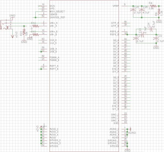
55 Appendix Circuit Schematics RF Frontend 51

56 FPGA ADC (AD9238) and FPGA (EP3C5E144) are connected with invisible connection since direct wiring on this schematic is complicated and Table 7 describes those connections. Table 7 FPGA pin assignment FPGA Pin # Target Device Target Pin # FPGA Pin # Target Device 52 Target Pin # FPGA Pin # Target Device Target Pin # 1 Audio Connector 1 34 AD AD AD AD AS connector 3 3 AD AD AD AD AD AD AS connector 9 50 AD AD
57 6 EPCS AD AD AD AD AD AS connector 8 55 AD AD EPCS AD AD AD AD AD AS connector 1 60 AD AD EPCS SST25VF512A FT245R AS connector 7 70 SST25VF512A FT245R EPCS SST25VF512A FT245R AS connector 5 72 LED FT245R JTAG connector 9 73 LED FT245R 9 18 JTAG connector 5 74 SST25VF512A FT245R 6 20 JTAG connector 3 76 LED FT245R 5 21 AS connector 6 77 SST25VF512A FT245R 3 22 Oscillator 3 79 LED FT245R 2 28 AD AD FT245R 1 30 AD AD FT245R AD AD FT245R AD AD Jumper 1 33 AD AD Jumper 2 ADC ADC (AD9238) and FPGA (EP3C5E144) are connected with invisible connection since direct wiring on this schematic is complicated and Table 7 describes those connections. 53
58 54

59 Power Distribution Network C++ Code for Data Collection main.cpp #include <iostream> #include "rs232.h" #include "logger.h" using namespace std; int main(int argc, char* argv[]) 55
60 RS232 receiver; receiver.port_open(); receiver.port_config(); receiver.port_status(); LOGGER log_file; cout << "Reading data from COM port, Ctrl+C to quit." log_file.open(); string frame_tmp; for(;;) frame_tmp = receiver.frame_get(); if(frame_tmp.empty() == 1) system("pause"); return(1); //cout << frame_tmp << endl; log_file.write( frame_tmp.append("\n") ); << endl; receiver.port_close(); system("pause"); return(0); logger.h #define FILE_SIZE_MAX #include <fstream> #include <iostream> #include <sstream> using namespace std; class LOGGER public: LOGGER(void); void open(void); 56
61 ; void write(string); void close(); private: string name_header; ofstream file_stream; string file_name; unsigned frame_counter; int file_counter; void file_control(void); LOGGER::LOGGER(void) frame_counter = 0; file_counter = -1; void LOGGER::open(void) cout << "Please enter the output file name\nname>"; cin >> name_header; file_counter = 0; file_name.assign(name_header); file_name.append("_0.log"); file_stream.open( file_name.c_str() ); cout << "Writting to file " << file_name << endl; void LOGGER::write(string _input) file_stream << _input; frame_counter++; if(frame_counter > FILE_SIZE_MAX) file_control(); frame_counter = 0; void LOGGER::file_control(void) 57
62 file_stream.close(); // close current file file_counter++; string _name_suffix; _name_suffix.assign("_"); std::stringstream _name_ss; _name_ss << file_counter; _name_suffix.append( _name_ss.str() ); _name_suffix.append(".log"); file_name.assign(name_header); file_name.append(_name_suffix); file_stream.open( file_name.c_str() ); cout << "Writting to file " << file_name << endl; rs232.h #include <iostream> #include <windows.h> #include <sys/timeb.h> #include <sstream> using namespace std; class RS232 public: int port_open(void); int port_config(void); void port_status(void); string frame_get(void); void port_close(void); private: HANDLE com_port_handle; COMMTIMEOUTS com_port_timeout; DCB com_port_config; string port_buffer; string port_time_last, port_time_new; string time_stamp(void); int port_read(void); ; // the time stame for last read opeartion 58
63 int RS232::port_open(void) // get the name of COM port from user string _port_number,_port_name="\\\\.\\com"; cout << "Please specify serial port: COM"; cin >> _port_number; _port_name.append(_port_number); // open COM port com_port_handle = CreateFile ( _port_name.c_str(), GENERIC_READ GENERIC_WRITE, 0, NULL, OPEN_EXISTING, 0, NULL ); // check status of COM port if( com_port_handle == INVALID_HANDLE_VALUE ) // cannot open COM port cout << "*** ERROR ***\tcannot open COM port" << endl; return(1); return(0); int RS232::port_config(void) // set timeouts com_port_timeout = 1, 100, 1000, 0, 0 ;//COMMTIMEOUTS _port_timeout = 1, 100, 1000, 0, 0 ; //DCB _port_config; if(!setcommtimeouts(com_port_handle, &com_port_timeout) ) cout << "*** WARNING ***\tset Timeout failed" << endl; // set DCB memset( &com_port_config, 0, sizeof(com_port_config) ); com_port_config.dcblength = sizeof(com_port_config); com_port_config.baudrate = ; com_port_config.fbinary = 1; 59
64 com_port_config.fdtrcontrol = DTR_CONTROL_ENABLE; com_port_config.frtscontrol = RTS_CONTROL_ENABLE; // com_port_config.foutxctsflow = 1; // com_port_config.frtscontrol = DTR_CONTROL_HANDSHAKE; com_port_config.parity = NOPARITY; com_port_config.stopbits = 1; com_port_config.bytesize = 8; if(!setcommstate(com_port_handle,&com_port_config)) cout << "*** WARNING ***\tset State failed" << endl; return(1); return(0); void RS232::port_status(void) cout << "Please confirm the following settings" << endl; cout << "\tbaud Rate: " << com_port_config.baudrate << endl; cout << "\tparity: " << (int)com_port_config.parity << endl; cout << "\tbyte Size: " << (int)com_port_config.bytesize << endl; cout << "\tstop Bits: " << (int)com_port_config.stopbits << endl; string RS232::frame_get(void) // check if there's an entire frame in the buffer int _location_start, _location_end, _read_flag, _residue_frag; string _frame; for(_residue_frag = 0;;) _location_start = port_buffer.find("*"); // locate the start of first frame _location_end = port_buffer.find(";"); // locate the end of first frame if( _location_start == 0 && _location_end > 0 ) // ideal case break; else if( _location_start > 0 ) // some trash exist in the front if(_location_end < 0) // no end char, we need read more data from port 60
65 _residue_frag = 1; port_buffer.erase(0, _location_start); // remove everthing before the frame continue; else port_buffer.clear(); _read_flag = port_read(); // if the buffer is empty, get some new data from COM port if( _read_flag == 0 ) cout << "*** ERROR ***\tcannot get new data from COM port" << endl; _frame.clear(); // return an empty string return(_frame); if(_residue_frag == 1) _frame.assign( port_time_last ); // add time stamp to the frame else _frame.assign( port_time_new ); // add time stamp to the frame _frame.append( port_buffer, _location_start, _location_end-_location_start+1 ); // copy the first frame to frame buffer port_buffer.erase(0,_location_end+3); // remove the first frame in the COM buffer return(_frame); void RS232::port_close(void) CloseHandle(com_port_handle); // generate time stamp string for current time string RS232::time_stamp(void) timeb _buffer; ftime(&_buffer); 61
66 std::stringstream _buffer_ss; _buffer_ss << (long)_buffer.time; _buffer_ss << (long)_buffer.millitm; std::string _output; _output = _buffer_ss.str(); switch( _output.length() ) case 13: _output.insert( _output.length()-3, "." ); break; case 12: _output.insert( _output.length()-2, ".0" ); break; case 11: _output.insert( _output.length()-1, ".00" ); break; default: break; return(_output); int RS232::port_read(void) int _read_flag; char _buffer_raw[512]; DWORD _read = 0; port_time_last = port_time_new; port_time_new = time_stamp(); _read_flag = ReadFile( com_port_handle, _buffer_raw, sizeof(_buffer_raw), &_read, NULL ); updated with the number of bytes read port_buffer.append( _buffer_raw, 0, sizeof(_buffer_raw) ); return(_read_flag); 62 // read is
67 C++ Code for Mode-S Decoding main.cpp #include <stdio.h> #include <stdlib.h> #include <iostream> #include "reader.h" #include "crc.h" #include "decoder.h" #include "writer.h" #include <time.h> using namespace std; int main(int argc, char *argv[]) string str_record, str_time, str_frame; unsigned cnt_total, cnt_good, cnt_useful; READER data_in; WRITER data_out; DECODER decode; data_in.open(); data_out.open(); CRC crc_t; for( cnt_total = cnt_good = cnt_useful = 0; ; cnt_total++ ) str_time = str_frame = ""; str_record = data_in.get(); if(str_record.empty()!= 0) // all data have been processed break; str_time.append(str_record, 0, 14); str_frame.append(str_record, 15, str_record.length()-16); if( crc_t.check(str_frame) == 0 ) if( decode.load(str_record) == 0 ) 63
68 data_out.write( decode.result().append("\n") ); cnt_useful++; cnt_good++; decode.end(); printf("total=%d\tgood=%d\tuseful=%d\t%.2f%%.\n", cnt_total, cnt_good, cnt_useful, (float)cnt_useful/(float)cnt_total*1000 ); data_in.close(); data_out.close(); system("pause"); return(0); reader.h #include <iostream> #include <fstream> #include <sstream> #define FILE_LIST_SIZE 32 using namespace std; struct FILENAME string header; int index; ; class READER public: READER(void); int open(void); int close(void); string get(void); private: FILENAME file_list[file_list_size]; string name_header, name; 64
69 ; ifstream file_stream; unsigned group_index, group_index_max, name_index, name_index_max; int file_control(void); READER::READER(void) name_index = -1; group_index = 0; int READER::open(void) int _group_number, _cnt; cout << "Please enter the number of file groups>"; cin >> _group_number; group_index_max = _group_number - 1; cout << "Please enter the input file header and index of last file, " << FILE_LIST_SIZE << " groups max." << endl; cout << "Such as: \"FileHeaderABC 95\"<enter>" << endl; for( _cnt = 0; (_cnt < _group_number) && (_cnt < FILE_LIST_SIZE) ; _cnt++ ) cout << "Group " << _cnt + 1 << ">"; cin >> file_list[_cnt].header; cin >> file_list[_cnt].index; return( file_control() ); int READER::file_control(void) if( name_index!= -1 group_index!= 0 ) // this is not the very first file file_stream.close(); name_index++; if( name_index > file_list[group_index].index ) // swith between file groups name_index = 0; group_index++; if( group_index > group_index_max ) // at the end of list 65
70 return(1); string _suffix = "_"; stringstream _suffix_ss; _suffix_ss << name_index; _suffix.append( _suffix_ss.str() ); _suffix.append(".log"); name.assign( file_list[group_index].header ); name.append(_suffix); file_stream.open( name.c_str() ); if( file_stream.good() ) cout << "Reading file " << name << endl; return(0); else return(-1); string READER::get(void) bool _flag; string _buffer; _flag = getline(file_stream, _buffer); if( _flag!= 1 ) if( file_control()!= 0 ) _buffer = ""; // return a empty string else return( get() ); return(_buffer); int READER::close(void) file_stream.close(); 66
71 crc.h [8] //#include "common.h" using namespace std; class CRC public: CRC(void); int check(string); private: int length; unsigned poly, crc_result, pi_raw; unsigned frame_char[14]; void str2char(string); // convert hex string into char which formed by two hex numbers unsigned crc(void); // calculate CRC unsigned str2num(string); ; CRC::CRC(void) poly = 0xFFFA0480; int CRC::check(string _frame) length = _frame.length(); if( (length!= 14) && (length!= 28) ) return(-1); // abort if format is bad str2char(_frame); crc_result = crc(); string _frame_pi; pi_raw = str2num( _frame_pi.append( _frame, length-6, 6 ) ); return( crc_result - pi_raw ); void CRC::str2char(string _frame) // e.g. input="2a30", output= 0x2A, 0x30 ; only support large case letter int _cnt, _frame_int[28]; for( _cnt = 0; _cnt < length; _cnt++ ) // convert hex number string into int array 67
72 _frame_int[_cnt] = _frame[_cnt] - 48; if( _frame_int[_cnt] > 15 ) _frame_int[_cnt] = _frame_int[_cnt] - 7; // small case use 39, large case use 7 /*if( _frame_int[_cnt] > 15 ) _frame_int[_cnt] = _frame_int[_cnt] - 32; */ for( _cnt = 0; _cnt < length/2; _cnt++ ) // convert int array into char array frame_char[_cnt] = _frame_int[_cnt*2+1] + _frame_int[_cnt*2]*16; unsigned CRC::crc(void) // for 112-bit only unsigned data, data1, data2; data = frame_char[0]<<24 frame_char[1]<<16 frame_char[2]<<8 frame_char[3]; data1 = frame_char[4]<<24 frame_char[5]<<16 frame_char[6]<<8 frame_char[7]; data2 = frame_char[8]<<24 frame_char[9]<<16 frame_char[10]<<8; unsigned cnt; if(length == 28) for( cnt = 0; cnt < 88; cnt++ ) if( (data & 0x )!= 0 ) data = data ^ poly; data = data << 1; if( (data1 & 0x )!= 0 ) data = data 1; data1 = data1 << 1; if( (data2 & 0x )!= 0 ) data1 = data1 1; data2 = data2 << 1; else for( cnt = 0; cnt < 32; cnt++ ) if( (data & 0x )!= 0 ) data = data ^ poly; data = data << 1; 68
73 return(data>>8); unsigned CRC::str2num(string _str) // e.g. input="2a30", output=0x2a30 int _cnt; unsigned _length, _frame_num[28], _num; _num = 0; _length = _str.length(); if( _length > 8 ) return(-1); // too long to process for( _cnt = 0; _cnt < _length; _cnt++ ) // convert hex number string _frame_num[_cnt] = _str[_cnt] - 48; if( _frame_num[_cnt] > 10 ) _frame_num[_cnt] = _frame_num[_cnt] - 7; // small case use 39, large case use 7 _num += ( _frame_num[_cnt] << 4*( _length - _cnt - 1 ) ); return(_num); decoder.h [9] #include <iostream> #include <sstream> #include <time.h> #include <math.h> #include <iomanip> // adjust output format #include "database.h" #include "counter.h" #define PI #define CPR_NZ 15.0 using namespace std; class DECODER 69
74 ; public: DECODER(void); int load(string); string result(void); int end(void); private: string raw_stamp, raw_frame, result_str; int length; int type_main, type_sub; unsigned str2num(string); string num2str(unsigned); // variable and functions for date and time string utc_msec_str, utc_str; // we are actually using local time instead of UTC unsigned time_stamp_sec; // unix time stamp for current frame int utc_year, utc_month, utc_day, utc_hour, utc_min, utc_sec, utc_msec; int time_stamp(void); string format_number(int); // decoding function DATABASE db_cpr; string df17(void); double cpr_nl(double); double cpr_max(double, double); // statistic and log COUNTER frame_counter; DECODER::DECODER(void) length = -1; raw_stamp = raw_frame = ""; int DECODER::load(string _record) string _buffer; // reset all parameters before start utc_year = utc_month = utc_day = utc_hour = utc_min = utc_sec = utc_msec = -1; type_main = type_sub = -1; result_str = ""; // set parameters for later process raw_stamp = _record.substr(0, 14); 70
75 raw_frame = _record.substr(15, _record.length()-16 ); length = raw_frame.length(); time_stamp(); type_main = str2num( raw_frame.substr(0,2) ) >> 3; // decode frame frame_counter.add(type_main); if(type_main!=17) return(-1); // only consider DF17 for this development phase // format result _buffer = df17(); if( _buffer.empty() == 0 ) result_str = utc_str; result_str.append( _buffer ); return(0); //cout << utc_str << raw_frame << endl; string DECODER::result(void) return( result_str ); unsigned DECODER::str2num(string _str) // e.g. input="2a30", output=0x2a30 int _cnt; unsigned _length, _frame_num[8], _num; _num = 0; _length = _str.length(); if( _length > 8 ) return(-1); // to long to process for( _cnt = 0; _cnt < _length; _cnt++ ) // convert hex number string _frame_num[_cnt] = _str[_cnt] - 48; if( _frame_num[_cnt] > 10 ) _frame_num[_cnt] = _frame_num[_cnt] - 7; // small case use 39, large case use 7 _num += ( _frame_num[_cnt] << 4*( _length - _cnt - 1 ) ); return(_num); 71
76 string DECODER::num2str(unsigned _in) // convert input number into 6-digit hex string int _cnt; char _number; stringstream _ss; for( _cnt = 5; _cnt >= 0; _cnt-- ) _number = ( ( _in & ( 0xf << (_cnt*4) ) ) >> (_cnt*4) ); if( _number > 9 ) _number += 7; // display as large case _number += 48; _ss << _number; return( _ss.str() ); // we are actually using local time instead of UTC int DECODER::time_stamp(void) // calculate date and time for the current frame // get number value of time stamp stringstream _buffer_s, _buffer_ms; _buffer_s << raw_stamp.substr(0,10); _buffer_s >> time_stamp_sec; utc_msec_str = raw_stamp.substr(11,3); // we need this string format msec later when write file _buffer_ms << utc_msec_str; _buffer_ms >> utc_msec; // convert time stamp into date and time struct tm * _time_struct; time_t _stamp = time_stamp_sec; _time_struct = localtime( &_stamp ); // set current time utc_year = _time_struct->tm_year ; utc_month = _time_struct->tm_mon + 1; utc_day = _time_struct->tm_mday; utc_hour = _time_struct->tm_hour; utc_min = _time_struct->tm_min; utc_sec = _time_struct->tm_sec; // generate output date/time string, e.g ,07:27:03.093, 72
77 stringstream _utc_ss; _utc_ss << utc_year << format_number(utc_month) << format_number(utc_day) << ","; _utc_ss << format_number(utc_hour) << ":" << format_number(utc_min) << ":" << format_number(utc_sec) << "." << utc_msec_str <<","; utc_str = _utc_ss.str(); string DECODER::format_number(int _number) stringstream _buffer_ss; string _buffer; _buffer_ss << _number; if( _number < 10 ) _buffer = "0"; _buffer.append( _buffer_ss.str() ); else _buffer = _buffer_ss.str(); return(_buffer); string DECODER::df17(void) unsigned _icao, _format, _altitude; unsigned _lat_cpr_0, _lat_cpr_1, _lon_cpr_0, _lon_cpr_1; // 0=even, 1=odd string _adsb, _adsb_db, _log; stringstream _buffer_ss; _icao = str2num( raw_frame.substr(2,6) ); _adsb = raw_frame.substr(8,14); type_sub = str2num( _adsb.substr(0,2) ) >> 3; if( type_sub >= 9 && type_sub <= 18 ) // only consider airbone position message at this development phase _format = ( str2num( _adsb.substr(5,1) ) & 0x4 ) >> 2; // get ADS-B format number // deode altitude data if( ( str2num( _adsb.substr(3,1) ) & 0x1 ) == 1 ) _altitude = ( ( ( str2num( _adsb.substr(2,2) ) >> 1 ) << 4 ) + str2num( _adsb.substr(4,1) ) ) * ; 73
78 else frame_counter.add(-2); cout << "ALT CODE Q=0" << endl; // search a different CPR format frame in database to form a pair for global decode _adsb_db = db_cpr.query(time_stamp_sec, utc_msec, _icao, _format, _adsb); if( _adsb_db.length()!= 14 ) // we got nothing from database return(""); // extract CPR formatted lat and lon information if( _format == 0 ) // current frame is even _lat_cpr_0 = ( str2num( _adsb.substr(5,5) ) & 0x3fffe ) >> 1; _lon_cpr_0 = str2num( _adsb.substr(9,5) ) & 0x1ffff; _lat_cpr_1 = ( str2num( _adsb_db.substr(5,5) ) & 0x3fffe ) >> 1; _lon_cpr_1 = str2num( _adsb_db.substr(9,5) ) & 0x1ffff; else _lat_cpr_1 = ( str2num( _adsb.substr(5,5) ) & 0x3fffe ) >> 1; _lon_cpr_1 = str2num( _adsb.substr(9,5) ) & 0x1ffff; _lat_cpr_0 = ( str2num( _adsb_db.substr(5,5) ) & 0x3fffe ) >> 1; _lon_cpr_0 = str2num( _adsb_db.substr(9,5) ) & 0x1ffff; // start decode CPR format data double yz0 = (double) _lat_cpr_0; double yz1 = (double) _lat_cpr_1; double xz0 = (double) _lon_cpr_0; double xz1 = (double) _lon_cpr_1; double dlat0 = 360.0/( 4.0*CPR_NZ ); double dlat1 = 360.0/( 4.0*CPR_NZ-1.0 ); double j = floor( (59.0*yz0-60.0*yz1)/pow(2.0,17.0) ); double rlat0 = dlat0*( fmod(j,60.0)+yz0/pow(2.0,17.0) ); double rlat1 = dlat1*( fmod(j,59.0)+yz1/pow(2.0,17.0) ); if( rlat0 > ) rlat0 = rlat ; rlat1 = rlat ; 74
79 if( cpr_nl(rlat0)!= cpr_nl(rlat1) ) frame_counter.add(-1); cout << "CPR decode ERROR" << endl; double n0 = cpr_max( cpr_nl(rlat0), 1.0); double n1 = cpr_max( cpr_nl(rlat1)-1.0, 1.0); double dlon0 = 360.0/n0; double dlon1 = 360.0/n1; double m = floor( ( xz0*(cpr_nl(rlat0)-1) - xz1*cpr_nl(rlat1) )/pow(2.0,17.0) ); double rlon0 = dlon0*( fmod(m,n0) + xz0/pow(2.0,17.0) ); double rlon1 = dlon1*( fmod(m,n1) + xz1/pow(2.0,17.0) ); if( rlon0 > ) rlon0 = rlon ; rlon1 = rlon ; // generate result string _buffer_ss << num2str( _icao ) << ","; _buffer_ss << fixed; if( _format ==0 ) // select the LAT and LON of the current frame instead of the one from database _buffer_ss << setprecision(5) << rlat0 << "," << setprecision(5) << rlon0 << "," << _altitude; else _buffer_ss << setprecision(5) << rlat1 << "," << setprecision(5) << rlon1 << "," << _altitude; //printf("icao=%x\tlat=%f\tlon=%f\talt=%d\n",_icao,rlat1,rlon1,_altitude); return( _buffer_ss.str() ); return(""); double DECODER::cpr_nl(double _lat) if( _lat < _lat > 90.0 ) return(-1.0); return( floor( 2.0*PI / acos( (1.0-cos(PI/2.0/CPR_NZ))/pow(cos(PI/180.0*fabs(_lat)),2.0) ) ) ); 75
80 double DECODER::cpr_max(double _i0, double _i1) if( _i0 > _i1 ) return(_i0); return(_i1); int DECODER::end(void) frame_counter.print(); database.h #define MAX_TIME_DIFFERENCE 15 // ICAO requires less than 10 seconds for a 1000 knot aircraft #define MAX_ITEM_NUMBER 512 // shold be twice as the total max number of aircraft in range using namespace std; struct DATABASE_ITEM unsigned time_sec, time_msec, icao, format; string adsb; ; class DATABASE public: DATABASE(void); string query(unsigned, unsigned, unsigned, unsigned, string); void status(void); private: int end_pointer, end_pointer_max; // pointer of the last record DATABASE_ITEM item[max_item_number]; unsigned format_not(unsigned); int search(unsigned, unsigned); int remove(int); 76
81 ; int update(unsigned, unsigned); DATABASE::DATABASE(void) int _cnt; end_pointer = -1; end_pointer_max = -1; for( _cnt = 0; _cnt < MAX_ITEM_NUMBER; _cnt++ ) item[_cnt].time_sec = -1; item[_cnt].time_msec = -1; item[_cnt].icao = -1; item[_cnt].format = -1; item[_cnt].adsb = ""; string DATABASE::query(unsigned _sec, unsigned _msec, unsigned _icao, unsigned _format, string _adsb) int _adr_diff, _adr_same; update( _sec, _msec ); // find an old frame which has same format and update it _adr_same = search(_icao, _format); if( _adr_same > -1 ) item[_adr_same].time_sec = _sec; item[_adr_same].time_msec = _msec; item[_adr_same].icao = _icao; item[_adr_same].format = _format; item[_adr_same].adsb = _adsb; else // if this is the first one in this format, save it if( end_pointer < MAX_ITEM_NUMBER-1 ) // if list is full, just rewrite the last record end_pointer++; item[end_pointer].time_sec = _sec; item[end_pointer].time_msec = _msec; item[end_pointer].icao = _icao; 77
82 item[end_pointer].format = _format; item[end_pointer].adsb = _adsb; // find a frame which has different format, e.g. _format=odd, find a even frame _adr_diff = search(_icao, format_not(_format) ); if( _adr_diff > -1 ) // if founded, return it and update record return( item[_adr_diff].adsb ); return("null"); void DATABASE::status(void) if( end_pointer > MAX_ITEM_NUMBER*0.9 ) cout << "\t*** WARNING ***\tdatabase is almost full." << endl; if( end_pointer > end_pointer_max ) end_pointer_max = end_pointer; cout << "\t*** USAGE ***\tnow=" << end_pointer+1 << "\tmax=" << end_pointer_max+1 << endl; unsigned DATABASE::format_not(unsigned _in) if( _in == 0 ) return(1); if( _in == 1 ) return(0); return(_in); int DATABASE::search(unsigned _icao, unsigned _format) int _cnt; for( _cnt = 0; _cnt <= end_pointer; _cnt++ ) if( item[_cnt].icao == _icao && item[_cnt].format == _format ) return(_cnt); 78
83 return(-1); int DATABASE::remove(int _adr) int _cnt; if( _adr < 0 _adr > end_pointer _adr >= MAX_ITEM_NUMBER ) return(-1); for( _cnt = _adr; _cnt <= end_pointer; _cnt++ ) item[_cnt] = item[_cnt+1]; end_pointer--; item[_cnt+1].time_sec = -1; item[_cnt+1].time_msec = -1; item[_cnt+1].icao = -1; item[_cnt+1].format = -1; item[_cnt+1].adsb = ""; return(0); int DATABASE::update(unsigned _sec, unsigned _msec) int _cnt; for( _cnt = 0; _cnt < end_pointer; _cnt++ ) if( _sec - item[_cnt].time_sec > MAX_TIME_DIFFERENCE +1 ) remove(_cnt); _cnt--; return(0); counter.h #include <iostream> 79
84 #include <iomanip> // adjust output format using namespace std; class COUNTER public: COUNTER(void); int add(int); void print(void); int reset(void); private: int type[32],error[32]; int total; ; COUNTER::COUNTER(void) for( int _cnt=0; _cnt<32; _cnt++ ) type[_cnt] = 0; for( int _cnt=0; _cnt<32; _cnt++ ) error[_cnt] = 0; total = 0; int COUNTER::add(int _item) if( _item > -1 && _item < 33 ) type[_item]++; total++; return(0); else if( _item > -33 && _item < 0 ) error[ abs(_item) - 1 ]++; total++; 80
85 return(0); else return(1); void COUNTER::print(void) int _cnt, _sum = 0; float _percent; cout << endl << endl << "*** STATISTICS ***" << endl; cout << "* ERRORS COUNT" << endl; cout << "CPR_ERROR=" << error[0] << "\talt_q_0=" << error[1] << endl; cout << endl << "* DF TYPES COUNT" << endl; cout << "type\t" << "count\t" << "percent" << endl; for( _cnt=0; _cnt<32; _cnt++ ) _percent = (float)type[_cnt]/(float)total*100; cout << fixed; cout << _cnt << "\t" << type[_cnt] << "\t" << setprecision(2) << _percent << endl; cout << endl; writer.h #define FILE_SIZE_MAX // #include <fstream> #include <iostream> #include <sstream> using namespace std; class WRITER public: WRITER(void); void open(void); void open(int); void write(string); void close(); 81
86 ; private: int flag_mode; string name_header; ofstream file_stream; string file_name; unsigned frame_counter; int file_counter; int file_control(void); WRITER::WRITER(void) frame_counter = 0; file_counter = -1; flag_mode = 0; void WRITER::open(void) cout << "Please enter the output file name\nname>"; cin >> name_header; file_counter = 0; file_name.assign(name_header); file_name.append("_0.log"); file_stream.open( file_name.c_str() ); cout << "Writting to file " << file_name << endl; void WRITER::open(int _mode) flag_mode = _mode; // in this mode (mode=1), nothing will print on the screen cin >> name_header; file_counter = 0; file_name.assign(name_header); file_name.append(".log"); file_stream.open( file_name.c_str() ); void WRITER::write(string _input) file_stream << _input; 82
87 frame_counter++; if( ( frame_counter > FILE_SIZE_MAX ) && ( flag_mode == 0 ) ) file_control(); frame_counter = 0; int WRITER::file_control(void) file_stream.close(); // close current file if( flag_mode == 1 ) // in log mode, only save to one file return(1); file_counter++; string _name_suffix; _name_suffix.assign("_"); std::stringstream _name_ss; _name_ss << file_counter; _name_suffix.append( _name_ss.str() ); _name_suffix.append(".log"); file_name.assign(name_header); file_name.append(_name_suffix); file_stream.open( file_name.c_str() ); cout << "Writting to file " << file_name << endl; void WRITER::close(void) file_stream.close(); 83

88 MATLAB Code for Data Analyze Receiver and Radar Data Processing Receiver_const.mat receiver_file_dz.m %% Read log file generated by PlanePlotter % output array fomatfor each row in the array % data_date_int, data_time_normal, data_icao_int, data_lat_int, data_lon_int, data_alt, -1, data_time_msecond_int, -1, -1, -1 % -1 are reserver position for storing future calculation result function [data_output, length, file_name] = receiver_file_dz() load receiver_const; file_name = input('please specify log file> ', 's'); file_id = fopen(file_name, 'r'); if(file_id == -1) fprintf('\n*** ERROR ***\ncannot open file.\n\n'); clear LAT_RADAR LON_RADAR ALT_RADAR RANGE_S RANGE_WE file_name file_id; data_output = -1; return; 84
AN-1370 APPLICATION NOTE
 APPLICATION NOTE One Technology Way P.O. Box 9106 Norwood, MA 02062-9106, U.S.A. Tel: 781.329.4700 Fax: 781.461.3113 www.analog.com Design Implementation of the ADF7242 Pmod Evaluation Board Using the
Keywords: GPS, receiver, GPS receiver, MAX2769, 2769, 1575MHz, Integrated GPS Receiver, Global Positioning System
 Maxim > Design Support > Technical Documents > User Guides > APP 3910 Keywords: GPS, receiver, GPS receiver, MAX2769, 2769, 1575MHz, Integrated GPS Receiver, Global Positioning System USER GUIDE 3910 User's
RADIO RECEIVERS ECE 3103 WIRELESS COMMUNICATION SYSTEMS
 RADIO RECEIVERS ECE 3103 WIRELESS COMMUNICATION SYSTEMS FUNCTIONS OF A RADIO RECEIVER The main functions of a radio receiver are: 1. To intercept the RF signal by using the receiver antenna 2. Select the
Getting started with OPENCORE NMR spectrometer. --- Installation and connection ---
 Getting started with OPENCORE NMR spectrometer --- Installation and connection --- Assembly USB The USB module is bus-powered. That is, DC power is provided by the personal computer via the USB cable.
Mode-S Receiver and ADS-B Decoder Group 24
 Mode-S Receiver and ADS-B Decoder Group 24 Sean Koceski, CpE Long Lam, CpE Michael Vose, CpE Spectrum Overload Digital UHF TV broadcast now borders aircraft traffic control frequencies. Devices intended
Session 3. CMOS RF IC Design Principles
 Session 3 CMOS RF IC Design Principles Session Delivered by: D. Varun 1 Session Topics Standards RF wireless communications Multi standard RF transceivers RF front end architectures Frequency down conversion
HY448 Sample Problems
 HY448 Sample Problems 10 November 2014 These sample problems include the material in the lectures and the guided lab exercises. 1 Part 1 1.1 Combining logarithmic quantities A carrier signal with power
Reducing Test Flights Using Simulated Targets and a Carefully Chosen Set-up
 Reducing Test Flights Using Simulated Targets and a Carefully Chosen Set-up Edition: 001 Date: 18-FEB-09 Status: Released DOCUMENT DESCRIPTION Document Title Reducing Test Flights: Using Simulated Targets
MAKING TRANSIENT ANTENNA MEASUREMENTS
 MAKING TRANSIENT ANTENNA MEASUREMENTS Roger Dygert, Steven R. Nichols MI Technologies, 1125 Satellite Boulevard, Suite 100 Suwanee, GA 30024-4629 ABSTRACT In addition to steady state performance, antennas
Range Considerations for RF Networks
 TI Technology Days 2010 Range Considerations for RF Networks Richard Wallace Abstract The antenna can be one of the most daunting components of wireless designs. Most information available relates to large
10 Secondary Surveillance Radar
 10 Secondary Surveillance Radar As we have just noted, the primary radar element of the ATC Surveillance Radar System provides detection of suitable targets with good accuracy in bearing and range measurement
Analysis of RF transceivers used in automotive
 Scientific Bulletin of Politehnica University Timisoara TRANSACTIONS on ELECTRONICS and COMMUNICATIONS Volume 60(74), Issue, 0 Analysis of RF transceivers used in automotive Camelia Loredana Ţeicu Abstract
RF/IF Terminology and Specs
 RF/IF Terminology and Specs Contributors: Brad Brannon John Greichen Leo McHugh Eamon Nash Eberhard Brunner 1 Terminology LNA - Low-Noise Amplifier. A specialized amplifier to boost the very small received
TSEK02: Radio Electronics Lecture 8: RX Nonlinearity Issues, Demodulation. Ted Johansson, EKS, ISY
 TSEK02: Radio Electronics Lecture 8: RX Nonlinearity Issues, Demodulation Ted Johansson, EKS, ISY RX Nonlinearity Issues: 2.2, 2.4 Demodulation: not in the book 2 RX nonlinearities System Nonlinearity
Keywords: ISM, RF, transmitter, short-range, RFIC, switching power amplifier, ETSI
 Maxim > Design Support > Technical Documents > Application Notes > Wireless and RF > APP 4929 Keywords: ISM, RF, transmitter, short-range, RFIC, switching power amplifier, ETSI APPLICATION NOTE 4929 Adapting
10 GHz Microwave Link
 10 GHz Microwave Link Project Project Objectives System System Functionality Testing Testing Procedures Cautions and Warnings Problems Encountered Recommendations Conclusion PROJECT OBJECTIVES Implement
PART MAX2605EUT-T MAX2606EUT-T MAX2607EUT-T MAX2608EUT-T MAX2609EUT-T TOP VIEW IND GND. Maxim Integrated Products 1
 19-1673; Rev 0a; 4/02 EVALUATION KIT MANUAL AVAILABLE 45MHz to 650MHz, Integrated IF General Description The are compact, high-performance intermediate-frequency (IF) voltage-controlled oscillators (VCOs)
4GHz / 6GHz Radiation Measurement System
 4GHz / 6GHz Radiation Measurement System The MegiQ Radiation Measurement System (RMS) is a compact test system that performs 3-axis radiation pattern measurement in non-anechoic spaces. With a frequency
Advances in Military Technology Vol. 5, No. 2, December Selection of Mode S Messages Using FPGA. P. Grecman * and M. Andrle
 AiMT Advances in Military Technology Vol. 5, No. 2, December 2010 Selection of Mode S Messages Using FPGA P. Grecman * and M. Andrle Department of Aerospace Electrical Systems, University of Defence, Brno,
TSEK02: Radio Electronics Lecture 8: RX Nonlinearity Issues, Demodulation. Ted Johansson, EKS, ISY
 TSEK02: Radio Electronics Lecture 8: RX Nonlinearity Issues, Demodulation Ted Johansson, EKS, ISY 2 RX Nonlinearity Issues, Demodulation RX nonlinearities (parts of 2.2) System Nonlinearity Sensitivity
Application Note 5525
 Using the Wafer Scale Packaged Detector in 2 to 6 GHz Applications Application Note 5525 Introduction The is a broadband directional coupler with integrated temperature compensated detector designed for
Using Frequency Diversity to Improve Measurement Speed Roger Dygert MI Technologies, 1125 Satellite Blvd., Suite 100 Suwanee, GA 30024
 Using Frequency Diversity to Improve Measurement Speed Roger Dygert MI Technologies, 1125 Satellite Blvd., Suite 1 Suwanee, GA 324 ABSTRACT Conventional antenna measurement systems use a multiplexer or
APPLICATION NOTE 3942 Optimize the Buffer Amplifier/ADC Connection
 Maxim > Design Support > Technical Documents > Application Notes > Communications Circuits > APP 3942 Maxim > Design Support > Technical Documents > Application Notes > High-Speed Interconnect > APP 3942
Radar Shield System Design
 University of California, Davis EEC 193 Final Project Report Radar Shield System Design Lit Po Kwong: lkwong853@gmail.com Yuyang Xie: szyuyxie@gmail.com Ivan Lee: yukchunglee@hotmail.com Ri Liang: joeliang914@gmail.com
HF Receivers, Part 2
 HF Receivers, Part 2 Superhet building blocks: AM, SSB/CW, FM receivers Adam Farson VA7OJ View an excellent tutorial on receivers NSARC HF Operators HF Receivers 2 1 The RF Amplifier (Preamp)! Typical
INVENTION DISCLOSURE- ELECTRONICS SUBJECT MATTER IMPEDANCE MATCHING ANTENNA-INTEGRATED HIGH-EFFICIENCY ENERGY HARVESTING CIRCUIT
 INVENTION DISCLOSURE- ELECTRONICS SUBJECT MATTER IMPEDANCE MATCHING ANTENNA-INTEGRATED HIGH-EFFICIENCY ENERGY HARVESTING CIRCUIT ABSTRACT: This paper describes the design of a high-efficiency energy harvesting
Maxim > Design Support > Technical Documents > Application Notes > Wireless and RF > APP 3571
 Maxim > Design Support > Technical Documents > Application Notes > Wireless and RF > APP 3571 Keywords: automotive keyless entry, MAX2640, LNA, 315MHz, RKE, stability, automotive, keyless entry APPLICATION
Exercise 1-3. Radar Antennas EXERCISE OBJECTIVE DISCUSSION OUTLINE DISCUSSION OF FUNDAMENTALS. Antenna types
 Exercise 1-3 Radar Antennas EXERCISE OBJECTIVE When you have completed this exercise, you will be familiar with the role of the antenna in a radar system. You will also be familiar with the intrinsic characteristics
Project ADS-B Receiver and Decoder
 Project ADS-B Receiver and Decoder About 50% of all commercial aircraft are transmitting their navigation information (position, speed, heading and more) on 1090MHz. The protocol and format is not encrypted
SynthNV - Signal Generator / Power Detector Combo
 SynthNV - Signal Generator / Power Detector Combo The Windfreak SynthNV is a 34.4MHz to 4.4GHz software tunable RF signal generator controlled and powered by a PC running Windows XP, Windows 7, or Android
USER MANUAL. ADS-B receiver PENTAGON
 USER MANUAL ADS-B receiver PENTAGON July, 2013 0 Contents 1. Introduction... 3 2. Hardware... 4 3. adsbpic-decoder... 5 4. Antennas... 5 5. Metal casing... 7 6. PC-Software... 10 6.1 Start the Software...
Applications. Operating Modes. Description. Part Number Description Package. Many to one. One to one Broadcast One to many
 RXQ2 - XXX GFSK MULTICHANNEL RADIO TRANSCEIVER Intelligent modem Transceiver Data Rates to 100 kbps Selectable Narrowband Channels Crystal controlled design Supply Voltage 3.3V Serial Data Interface with
Modeling Physical PCB Effects 5&
 Abstract Getting logical designs to meet specifications is the first step in creating a manufacturable design. Getting the physical design to work is the next step. The physical effects of PCB materials,
Third-Method Narrowband Direct Upconverter for the LF / MF Bands
 Third-Method Narrowband Direct Upconverter for the LF / MF Bands Introduction Andy Talbot G4JNT February 2016 Previous designs for upconverters from audio generated from a soundcard to RF have been published
CHAPTER 4. Practical Design
 CHAPTER 4 Practical Design The results in Chapter 3 indicate that the 2-D CCS TL can be used to synthesize a wider range of characteristic impedance, flatten propagation characteristics, and place passive
MITIGATING INTERFERENCE ON AN OUTDOOR RANGE
 MITIGATING INTERFERENCE ON AN OUTDOOR RANGE Roger Dygert MI Technologies Suwanee, GA 30024 rdygert@mi-technologies.com ABSTRACT Making measurements on an outdoor range can be challenging for many reasons,
NANOSCALE IMPULSE RADAR
 NANOSCALE IMPULSE RADAR NVA6X00 Impulse Radar Transceiver and Development Kit 2012.4.20 laon@laonuri.com 1 NVA6000 The Novelda NVA6000 is a single-die CMOS chip that delivers high performance, low power,
Dartmouth College LF-HF Receiver May 10, 1996
 AGO Field Manual Dartmouth College LF-HF Receiver May 10, 1996 1 Introduction Many studies of radiowave propagation have been performed in the LF/MF/HF radio bands, but relatively few systematic surveys
UM User manual for the BGU7004 GPS LNA evaluation board. Document information. Keywords LNA, GPS, BGU7004. Abstract
 User manual for the BGU7004 GPS LNA evaluation board Rev. 1.0 14 June 2011 User manual Document information Info Keywords Abstract Content LNA, GPS, BGU7004 This document explains the BGU7004 AEC-Q100
2 Gain Variation from the Receiver Output through the IF Path
 EVLA Memo #185 Bandwidth- and Frequency-Dependent Effects in the T34 Total Power Detector Keith Morris September 17, 214 1 Introduction The EVLA Intermediate Frequency (IF) system employs a system of power
ATF High Intercept Low Noise Amplifier for the MHz PCS Band using the Enhancement Mode PHEMT
 ATF-54143 High Intercept Low Noise Amplifier for the 185 191 MHz PCS Band using the Enhancement Mode PHEMT Application Note 1222 Introduction Avago Technologies ATF-54143 is a low noise enhancement mode
Technical Standard Order
 Department of Transportation Federal Aviation Administration Aircraft Certification Service Washington, DC TSO-C74c Date: 2/20/73 Technical Standard Order Subject: TSO-C74c, AIRBORNE ATC TRANSPONDER EQUIPMENT
GPS/GNSS Front-End Amplifier
 EVALUATION KIT AVAILABLE MAX2678 General Description The MAX2678 GPS/GNSS front-end amplifier IC is designed for automotive and marine GPS/GNSS satellite navigation antenna modules, or for any application
Signal Processing and Display of LFMCW Radar on a Chip
 Signal Processing and Display of LFMCW Radar on a Chip Abstract The tremendous progress in embedded systems helped in the design and implementation of complex compact equipment. This progress may help
The Discussion of this exercise covers the following points:
 Exercise 3-2 Frequency-Modulated CW Radar EXERCISE OBJECTIVE When you have completed this exercise, you will be familiar with FM ranging using frequency-modulated continuous-wave (FM-CW) radar. DISCUSSION
Agilent AN 1275 Automatic Frequency Settling Time Measurement Speeds Time-to-Market for RF Designs
 Agilent AN 1275 Automatic Frequency Settling Time Measurement Speeds Time-to-Market for RF Designs Application Note Fast, accurate synthesizer switching and settling are key performance requirements in
BPSK_DEMOD. Binary-PSK Demodulator Rev Key Design Features. Block Diagram. Applications. General Description. Generic Parameters
 Key Design Features Block Diagram Synthesizable, technology independent VHDL IP Core reset 16-bit signed input data samples Automatic carrier acquisition with no complex setup required User specified design
DESCRIPTIO FEATURES APPLICATIO S. LT GHz to 2.7GHz Receiver Front End TYPICAL APPLICATIO
 1.GHz to 2.GHz Receiver Front End FEATURES 1.V to 5.25V Supply Dual LNA Gain Setting: +13.5dB/ db at Double-Balanced Mixer Internal LO Buffer LNA Input Internally Matched Low Supply Current: 23mA Low Shutdown
Application Note 5480
 ALM-2712 Ultra Low-Noise GPS Amplifier with Pre- and Post-Filter Application Note 548 Introduction The ALM-2712 is a GPS front-end module which consists of a low noise amplifier with pre- and post-filters.
FlexDDS-NG DUAL. Dual-Channel 400 MHz Agile Waveform Generator
 FlexDDS-NG DUAL Dual-Channel 400 MHz Agile Waveform Generator Excellent signal quality Rapid parameter changes Phase-continuous sweeps High speed analog modulation Wieserlabs UG www.wieserlabs.com FlexDDS-NG
Gentec-EO USA. T-RAD-USB Users Manual. T-Rad-USB Operating Instructions /15/2010 Page 1 of 24
 Gentec-EO USA T-RAD-USB Users Manual Gentec-EO USA 5825 Jean Road Center Lake Oswego, Oregon, 97035 503-697-1870 voice 503-697-0633 fax 121-201795 11/15/2010 Page 1 of 24 System Overview Welcome to the
External Source Control
 External Source Control X-Series Signal Analyzers Option ESC DEMO GUIDE Introduction External source control for X-Series signal analyzers (Option ESC) allows the Keysight PXA, MXA, EXA, and CXA to control
UNIT-1. Basic signal processing operations in digital communication
 UNIT-1 Lecture-1 Basic signal processing operations in digital communication The three basic elements of every communication systems are Transmitter, Receiver and Channel. The Overall purpose of this system
Monitoring Station for GNSS and SBAS
 Monitoring Station for GNSS and SBAS Pavel Kovář, Czech Technical University in Prague Josef Špaček, Czech Technical University in Prague Libor Seidl, Czech Technical University in Prague Pavel Puričer,
Maxim Integrated Products 1
 19-3533; Rev 0; 1/05 MAX9996 Evaluation Kit General Description The MAX9996 evaluation kit (EV kit) simplifies the evaluation of the MAX9996 UMTS, DCS, and PCS base-station downconversion mixer. It is
Compact Series: S5065 & S5085 Vector Network Analyzers KEY FEATURES
 Compact Series: S5065 & S5085 Vector Network Analyzers KEY FEATURES Frequency range: 9 khz - 6.5 or 8.5 GHz Measured parameters: S11, S12, S21, S22 Wide output power adjustment range: -50 dbm to +5 dbm
High Level Design Group: RF Detection Group Members: Joey Py e, André Magill, Shane Ryan, John Docalovich, Zack Bennett Advisor: Dr.
 Group: RF Detection Group Members: Joey Py e, André Magill, Shane Ryan, John Docalovich, Zack Bennett Advisor: Dr. Jonathan Chisum Table of Contents 1 Introduction 3 2 Problem Statement and Proposed Solution
ADI 2006 RF Seminar. Chapter II RF/IF Components and Specifications for Receivers
 ADI 2006 RF Seminar Chapter II RF/IF Components and Specifications for Receivers 1 RF/IF Components and Specifications for Receivers Fixed Gain and Variable Gain Amplifiers IQ Demodulators Analog-to-Digital
HMC1044LP3E. Programmable Harmonic Filters - SMT. Functional Diagram. General Description
 Typical Applications The HMC144LP3E is ideal for wideband transceiver harmonic filtering applications including: Filtering lo Harmonics to Reduce Modulator Sideband Rejection & Demodulator Image Rejection
6.115 Final Project Proposal: An RFID Access Control System
 6.115 Final Project Proposal: An RFID Access Control System Christopher Merrill April 24, 2012 Abstract The goal of this nal project is to implement a device to read standard 125 khz RFID cards using the
CONDOR C1919 GPS RECEIVER MODULE technical notes GENERAL OVERVIEW
 CONDOR C1919 GPS RECEIVER MODULE TECHNICAL HIGHLIGHTS Receiver: GPS L1 frequency (17. MHz), C/A code, -channel continuous tracking NMEA output and input: serial port On-board low noise amplifier GENERAL
Preliminary Product Overview
 Preliminary Product Overview Features DC to > 3 GHz Frequency Range 25 Watt (CW), 200W (Pulsed) Max Power Handling Low On-State Insertion Loss, typical 0.3 db @ 3 GHz Low On-State Resistance < 0.75 Ω 25dB
Keysight Technologies Making Accurate Intermodulation Distortion Measurements with the PNA-X Network Analyzer, 10 MHz to 26.5 GHz
 Keysight Technologies Making Accurate Intermodulation Distortion Measurements with the PNA-X Network Analyzer, 10 MHz to 26.5 GHz Application Note Overview This application note describes accuracy considerations
ROM/UDF CPU I/O I/O I/O RAM
 DATA BUSSES INTRODUCTION The avionics systems on aircraft frequently contain general purpose computer components which perform certain processing functions, then relay this information to other systems.
Maxim Integrated Products 1
 19-0569; Rev 0; 5/06 MAX2041 Evaluation Kit General Description The MAX2041 evaluation kit (EV kit) simplifies the evaluation of the MAX2041 UMTS, DCS, and PCS base-station up/downconversion mixer. It
Receiver Architecture
 Receiver Architecture Receiver basics Channel selection why not at RF? BPF first or LNA first? Direct digitization of RF signal Receiver architectures Sub-sampling receiver noise problem Heterodyne receiver
ADVANCED EMBEDDED MONITORING SYSTEM FOR ELECTROMAGNETIC RADIATION
 98 Chapter-5 ADVANCED EMBEDDED MONITORING SYSTEM FOR ELECTROMAGNETIC RADIATION 99 CHAPTER-5 Chapter 5: ADVANCED EMBEDDED MONITORING SYSTEM FOR ELECTROMAGNETIC RADIATION S.No Name of the Sub-Title Page
S-Band 2.4GHz FMCW Radar
 S-Band 2.4GHz FMCW Radar Iulian Rosu, YO3DAC / VA3IUL, Filip Rosu, YO3JMK, http://qsl.net/va3iul A Radar detects the presence of objects and locates their position in space by transmitting electromagnetic
Keysight Technologies Pulsed Antenna Measurements Using PNA Network Analyzers
 Keysight Technologies Pulsed Antenna Measurements Using PNA Network Analyzers White Paper Abstract This paper presents advances in the instrumentation techniques that can be used for the measurement and
Impact of ATC transponder transmission to onboard GPS-L5 signal environment
 SCRSP-WG IP-A10 18 May 2006 SURVEILLANCE AND CONFLICT RESOLUTION SYSTEMS PANEL (SCRSP) TENTH MEETING WG-A Montreal, May, 2006 WG-A Agenda Item 9 Any Other Bussiness Impact of ATC transponder transmission
TAPR TICC Timestamping Counter Operation Manual. Introduction
 TAPR TICC Timestamping Counter Operation Manual Revised: 23 November 2016 2016 Tucson Amateur Packet Radio Corporation Introduction The TAPR TICC is a two-channel timestamping counter ("TSC") implemented
DEMO CIRCUIT 1057 LT6411 AND LTC2249 ADC QUICK START GUIDE LT6411 High-Speed ADC Driver Combo Board DESCRIPTION QUICK START PROCEDURE
 DESCRIPTION Demonstration circuit 1057 is a reference design featuring Linear Technology Corporation s LT6411 High Speed Amplifier/ADC Driver with an on-board LTC2249 14-bit, 80MSPS ADC. DC1057 demonstrates
Single Conversion LF Upconverter Andy Talbot G4JNT Jan 2009
 Single Conversion LF Upconverter Andy Talbot G4JNT Jan 2009 Mark 2 Version Oct 2010, see Appendix, Page 8 This upconverter is designed to directly translate the output from a soundcard from a PC running
Preamplifiers for Callisto Solar Radio Spectrometer
 Preamplifiers for Callisto Solar Radio Spectrometer Whitham Reeve and Christian Monstein 1. Introduction We investigated the performance of three amplifiers (figure 1) for Callisto applications by measuring
SC5307A/SC5308A 100 khz to 6 GHz RF Downconverter. Datasheet SignalCore, Inc.
 SC5307A/SC5308A 100 khz to 6 GHz RF Downconverter Datasheet 2017 SignalCore, Inc. support@signalcore.com P RODUCT S PECIFICATIONS Definition of Terms The following terms are used throughout this datasheet
Narrow Pulse Measurements on Vector Network Analyzers
 Narrow Pulse Measurements on Vector Network Analyzers Bert Schluper Nearfield Systems Inc. Torrance, CA, USA bschluper@nearfield.com Abstract - This paper investigates practical aspects of measuring antennas
USER OPERATION AND MAINTENANCE MANUAL
 46 Robezu str. LV-1004 Riga Latvia Phone: +371-7-065-100, Fax: +371-7-065-102 Mm-wave Division in St. Petersburg, Russia Phone: +7-812-326-5924, Fax: +7-812-326-1060 USER OPERATION AND MAINTENANCE MANUAL
ABA GHz Broadband Silicon RFIC Amplifier. Application Note 1349
 ABA-52563 3.5 GHz Broadband Silicon RFIC Amplifier Application Note 1349 Introduction Avago Technologies ABA-52563 is a low current silicon gain block RFIC amplifier housed in a 6-lead SC 70 (SOT- 363)
Measurement Procedure & Test Equipment Used
 Measurement Procedure & Test Equipment Used Except where otherwise stated, all measurements are made following the Electronic Industries Association (EIA) Minimum Standard for Portable/Personal Land Mobile
Modular Test Approaches for SSR Signal Analysis in IFF Applications
 Modular Test Approaches for SSR Signal Analysis in IFF Applications Military radar applications call for highly specialized test equipment Radar signal analysis applications require highly specialized
DEMO CIRCUIT 1004 ADC DRIVER AND 7X7MM HIGH-PERFORMANCE ADC QUICK START GUIDE ADC Driver and 7x7mm High-Performance ADC DESCRIPTION
 DEMO CIRCUIT 1004 QUICK START GUIDE ADC Driver and 7x7mm High-Performance ADC DESCRIPTION Demonstration circuit 1004 is a reference design featuring Linear Technology Corporation s Analog- Digital Converter
Radio Frequency Power Meter Design Project
 Radio Frequency Power Meter Design Project Timothy Holt and Andrew Milks University of Akron, Akron Ohio Abstract This student paper discusses a radio frequency power meter developed and prototyped as
DSA700 Series Spectrum Analyzer
 DSA700 Series Spectrum Analyzer Product Features: All-Digital IF Technology Frequency Range from 100 khz up to 1 GHz Min. -155 dbm Displayed Average Noise Level (Typ.) Min.
Integrators, differentiators, and simple filters
 BEE 233 Laboratory-4 Integrators, differentiators, and simple filters 1. Objectives Analyze and measure characteristics of circuits built with opamps. Design and test circuits with opamps. Plot gain vs.
Preliminary RFI Survey for IIP
 Preliminary RFI Survey for IIP Steven W. Ellingson June 11, 2002 1 Introduction This report describes a preliminary survey of radio frequency interference (RFI) made in support of ESL s IIP radiometer
1. Explain how Doppler direction is identified with FMCW radar. Fig Block diagram of FM-CW radar. f b (up) = f r - f d. f b (down) = f r + f d
 = f r - f d. f b (down) = f r + f d") 1. Explain how Doppler direction is identified with FMCW radar. A block diagram illustrating the principle of the FM-CW radar is shown in Fig. 4.1.1 A portion of the transmitter signal acts as the reference
1. Explain how Doppler direction is identified with FMCW radar. A block diagram illustrating the principle of the FM-CW radar is shown in Fig. 4.1.1 A portion of the transmitter signal acts as the reference
EITN90 Radar and Remote Sensing Lab 2
 EITN90 Radar and Remote Sensing Lab 2 February 8, 2018 1 Learning outcomes This lab demonstrates the basic operation of a frequency modulated continuous wave (FMCW) radar, capable of range and velocity
EFFECT OF SHIELDING ON CABLE RF INGRESS MEASUREMENTS LARRY COHEN
 EFFECT OF SHIELDING ON CABLE RF INGRESS MEASUREMENTS LARRY COHEN OVERVIEW Purpose: Examine the common-mode and differential RF ingress levels of 4-pair UTP, F/UTP, and F/FTP cables at an (RJ45) MDI port
SC5407A/SC5408A 100 khz to 6 GHz RF Upconverter. Datasheet. Rev SignalCore, Inc.
 SC5407A/SC5408A 100 khz to 6 GHz RF Upconverter Datasheet Rev 1.2 2017 SignalCore, Inc. support@signalcore.com P R O D U C T S P E C I F I C A T I O N S Definition of Terms The following terms are used
3250 Series Spectrum Analyzer
 The most important thing we build is trust ADVANCED ELECTRONIC SOLUTIONS AVIATION SERVICES COMMUNICATIONS AND CONNECTIVITY MISSION SYSTEMS 3250 Series Spectrum Analyzer > Agenda Introduction
Understanding Mixers Terms Defined, and Measuring Performance
 Understanding Mixers Terms Defined, and Measuring Performance Mixer Terms Defined Statistical Processing Applied to Mixers Today's stringent demands for precise electronic systems place a heavy burden
FCC and ETSI Requirements for Short-Range UHF ASK- Modulated Transmitters
 From December 2005 High Frequency Electronics Copyright 2005 Summit Technical Media FCC and ETSI Requirements for Short-Range UHF ASK- Modulated Transmitters By Larry Burgess Maxim Integrated Products
TRXQ1 RXQ1 FM NARROW BAND TRANSCEIVERS. RXQ1 Version. Applications. TRXQ1 Version
 RF Transceiver or Intelligent Modem Versions Host Data Rate upto 19,200 Baud Data Rates to 20 K baud. 2 Selectable RF Channels Narrowband Crystal Controlled Optimal Range 200m Supply Voltage 3-5V Very
Advances in Antenna Measurement Instrumentation and Systems
 Advances in Antenna Measurement Instrumentation and Systems Steven R. Nichols, Roger Dygert, David Wayne MI Technologies Suwanee, Georgia, USA Abstract Since the early days of antenna pattern recorders,
Wide-Band Two-Stage GaAs LNA for Radio Astronomy
 Progress In Electromagnetics Research C, Vol. 56, 119 124, 215 Wide-Band Two-Stage GaAs LNA for Radio Astronomy Jim Kulyk 1,GeWu 2, Leonid Belostotski 2, *, and James W. Haslett 2 Abstract This paper presents
Chapter-1: Introduction
 Chapter-1: Introduction The purpose of a Communication System is to transport an information bearing signal from a source to a user destination via a communication channel. MODEL OF A COMMUNICATION SYSTEM
AST-GPSRF. GPS / Galileo RF Downconverter GENERAL DESCRIPTION FEATURES APPLICATIONS FUNCTIONAL BLOCK DIAGRAM. Preliminary Technical Data
 FEATURES Single chip GPS / Galileo downconverter GPS L1 band C/A code (1575.42 MHz) receiver GALILEO L1 band OS code (1575.42 MHz) receiver 2.7 V to 3.3 V power supply On-chip LNA On-chip PLL including
Sharing Considerations Between Small Cells and Geostationary Satellite Networks in the Fixed-Satellite Service in the GHz Frequency Band
 Sharing Considerations Between Small Cells and Geostationary Satellite Networks in the Fixed-Satellite Service in the 3.4-4.2 GHz Frequency Band Executive Summary The Satellite Industry Association ( SIA
QLG1 GPS Receiver kit
 QLG1 GPS Receiver kit 1. Introduction Thank you for purchasing the QRP Labs QLG1 GPS Receiver kit. This kit will provide a highly sensitive, highly accurate GPS receiver module, using the popular MediaTek
Scalable Ionospheric Analyser SIA 24/6
 Scalable Ionospheric Analyser SIA 24/6 Technical Overview Functional description The ATRAD Scalable Ionospheric Analyser SIA24/6 is designed to observe ionospheric irregularities and their drift in the