TE 0224 ANALOG COMMUNICATION LAB. Laboratory Manual
|
|
|
- Edwin Powers
- 6 years ago
- Views:
Transcription

1 TE 0224 ANALOG COMMUNICATION LAB Laboratory Manual DEPARTMENT OF TELECOMMUNICATION ENGINEERING SRM UNIVERSITY S.R.M. NAGAR, KATTANKULATHUR FOR PRIVATE CIRCULATION ONLY ALL RIGHTS RESERVED
2 DEPARTMENT OF TELECOMMUNICATION ENGINEERING TE0224 ANALOG COMMUNICATION LAB ( ) Revision No: 2 Date: PREPARED BY, Mrs.Kavitha Narayanan Mrs.S.Murugaveni HOD/TCE
3 TEO224 ANALOG COMMUNICATION LAB List of Experiments 1. AM Modulation and Demodulation(Envelope Detector) 2. FM Modulation using PLL 3. Pulse Amplitude Modulation and Demodulation 4. Pre-emphasis and De-emphasis 5. Analog Multiplexing. 6. Study of FM detection 7. Amplitude Modulation using Pspice 8. AM Modulation using Matlab 9. FM Modulation using Matlab
4 AIM 1. AM MODULATOR & ENVELOPE DETECTOR To study the amplitude modulation and demodulation and to calculate the modulation index values for various modulating voltages APPARATUS REQUIRED 1. Transistor BC Resistors 3. Capacitors 4. AFO 5. CRO 6. Diode OA79 7. Millimeter 8. Regulated power supply 9. Breadboard and connecting wires THEORY Modulation is defined as the process by which some characteristics of a carrier signal is varied in accordance with a modulating signal. The base band signal is referred to as the modulating signal and the output of the modulation process is called as the modulation signal. Amplitude modulation is defined as the process in which is the amplitude of the carrier wave is varied about a means values linearly with the base band signal. The envelope of the modulating wave has the same shape as the base band signal provided the following two requirements are satisfied (1). the carrier frequency fc must be much greater then the highest frequency components fm of the message signal m (t) i.e. fc >> fm (II) The modulation index must be less than unity. if the modulation index is greater than unity, the carrier wave becomes over modulated. PROCEDURE 1. The circuit connection is made as shown in the circuit. 2. The power supply is connected to the collector of the transistor 3. Modulated Output is taken from the collector of the Transistor 4. Calculate Vmax and Vmin from the Output
5
6
7
8 Vc = 63mv fc = 500Khz fm = 1Khz Modulating signal Vm(v) (V) Emax(V) Modulation index M = Emax-Emin x 100 Emax + Emin AM DETECTION THEORY: The process of detection provides a means of recovering the modulating Signal from modulating signal. Demodulation is the reverse process of modulation. The detector circuit is employed to separate the carrier wave and eliminate the side bands. Since the envelope of an AM wave has the same shape as the message, independent of the carrier frequency and phase, demodulation can be accomplished by extracting envelope. An increased time constant RC results in a marginal output follows the modulation envelope. A further increase in time constant the discharge curve become horizontal if the rate of modulation envelope during negative half cycle of the modulation voltage is faster than the rate of voltage RC combination,the output fails to follow the modulation resulting distorted output is called as diagonal clipping : this will occur even high modulation index. The depth of modulation at the detector output greater than unity and circuit impedance is less than circuit load (Rl > Zm) results in clipping of negative peaks of modulating signal. It is called negative clipping
9 PROCEDURE 1. T he circuit connection are made as shown in the circuit diagram. 2. The amplitude modulated signal from AM generator is give as input to the circuit. 3. The demodulated output is observed on the CRO 4. The various values modulating voltage signal frequency corresponding demodulated voltage and frequency are noted and the readings are tabulated. SAMPLE READING Fc = 500 KHz fm = 1 KHz Emin (v) Emax (V) Em(p-p) Modulation index M = Emax-Emin x 100 Emax + Emin RESULT: Thus the amplitude modulation and demodulation circuit were designed and the modulation index for various modulating voltage were calculated.
10 REVIEW QUESTIONS 1. Define Modulation. 2. What is modulation index? 3. Differentiate under modulation & over modulation. 4. List the advantages of AM modulation. 5. What are the different AM modulations Techniques? 6. What is detector? 7. When Diagonal clipping and Negative clipping occur in demodulation and how it is overcome?
11 AIM: 2. FREQUENCY MODULATION To generate a frequency modulated wave-using IC 566 APPARATUS REQUIRED 1. AFO 2. IC NE Resistors 4. Capacitor 5. CRO 6. Bread board and connection 7. RPS THEORY: Frequency modulation is a process of changing the frequency of a carrier wave in accordance with the slowly varying base band signal. The main advantage of this modulation is that it can provide better discrimination against noise. FREQUENCY MODULATION USING IC 566 A VCO is a circuit that provides an oscillating signal whose frequency can be adjusted over a control by Dc voltage. VCO can generate both square and triangular Wave signal whose frequency is set by an external capacitor and resistor and then varied by an applied DC voltage. IC 566 contains a current source to charge and discharge an external capacitor C1 at a rate set by an external resistor. R1 and a modulating DC output voltage. The Schmitt trigger circuit present in the IC is used to switch the current source between charge and discharge capacitor and triangular voltage developed across the capacitor and the square wave from the Schmitt trigger are provide as the output of the buffer amplifier. The R2 and R3 combination is a voltage divider, the voltage VC must be in the range ¾ VCC < VC < VCC. The modulating voltage must be less than ¾ VCC the frequency Fc can be calculated using the formula Fo = 2 (Vcc-Vc) R1 C1 Vcc For a fixed value of Vc and a constant C1 the frequency can be varied at 10:1 similarly for a constant R! C1 product value the frequency modulation can be done at 10:1 ratio
12
13
14 FORMULA: Modulation index: β = f/fm where f = Fmax Fmin /2 PROCEDURE: 1. The circuit connection is made as shown in the circuit diagram. 2. The modulating signal FM is given from an AFO (1KHZ) 3. For various values of modulating voltage Vm the values of Fmax and Fmin are noted 4. The values of the modulation index are calculated. SAMPLE READING V m T min T max F max F min Modulation Index Β = / f / fm , RESULTS: The FM circuit using IC566 was designed and the modulation index for practical and Theoretical.
15 REVIEW QUESTIONS 1. Define Frequency Modulation. 2. What is Frequency deviation? 3. Differentiate under modulation & over modulation. 4. List the advantages of FM modulation over AM modulation. 5. What are the different AM modulations Techniques? 6. What is detector? 7. When Diagonal clipping and Negative clipping occur in demodulation and how it is overcome?
16 3. PULSE AMPLITUDE MODULATION & DEMODULATION AIM: To study and obtain pulse amplitude modulation and demodulation APPARATUS REQUIRED 1. Transistor 2. AFO 3. IC NE Resistors 5. Capacitor 5. CRO 6. RPS THEORY: Pulse amplitude modulation is a scheme, which alters the amplitude of regularly spaced rectangular pulses in accordance with the instantaneous values of a continuous message signal. Then amplitude of the modulated pulses represents the amplitude of the intelligence. A train of very short pulses of constant amplitude and fast repetition rate is chosen the amplitude of these pulse is made to vary in accordance with that of a slower modulating signal the result is that of multiplying the train by the modulating signal the envelope of the pulse height corresponds to the modulating wave.the Pam wave contain upper and lower side band frequencies.besides the modulating and pulse signals. The demodulated PAM waves, the signal is passed through a low pass filter having a cut off frequencies equal to the highest frequency in the modulating signal. At the output of the filter is available the modulating signal along with the DC component PAM has the same signal to noise ratio as AM and so it is not employed in practical circuits PROCEDURE: MODULATION
17 1. Make the circuit as shown in circuit diagram fig A 2. Set the pulse generated s output to be 41vpp at 100HZ 3. Set AFO s output at 2 vpp 100HZ 4. Observe the output wave form on a CRO 5. Tabulate the reading.
18 DEMODULATION: 1. Connect the circuit as shown in fig (b) 2. Given the modulated output with AFO used to the input of the circuit. 3. Vary the potentiometer so that modulating signal is obtained. 4. Measure the amplitude of the signal and verify with that of the input.
19 SAMPLE READING: PAM Modulating voltage Vm (V) Pulse Amplitude modulation (V) SAMPLE READING: DEMODULATION Modulating voltage Vm (V) Pulse Amplitude demodulation (V) RESULT: The pulse amplitude modulation circuit is circuit assembled and studied and demodulated wave also done.
20 AIM: 4. PRE EMPHASIS AND DE-EMPHASIS CIRCUITS To study and test the chateristics of pre-emphasis and de-emphasis circuits APPARATUS REQUIRED 1. Transistor 2. AFO 3. IC NE Resistors 5. Capacitor 5. CRO 6. RPS THEORY: PRE-EMPHASIS CIRCUITS The circuits are the transmitting side of the frequency modulator. It is used to increase the gain of the higher frequency component as the input signal frequency increased, the impendence of the collector voltage increase. If the signal frequency is lesser then the impendence decrease which increase the collector current and hence decrease the voltage. DE-EMPHASIS CIRCUITS: The circuit is placed at the receiving side. It acts as allow pass filter. The boosting gain for higher frequency signal in the transmitting side is done by the pre-emphasis circuit is filtered to the same value by the low pass filter. The cut off frequency is given by the formula Fc = 1/2π RC

21 Where R = 2 π fc L DESIGN FORMULA: Fc = 1/2 π R C (assume =R = 10 KΩ, C = 0.01μf) R = 2 π fc L; L = R/2 π fc
22 PROCEDURE: 1. The circuit connection are made as shown in the circuit diagram for the preemphasis and de-emphasis circuits 2. A power supply of 10V is given to the circuit
23 3. For a constant value of input voltage the values of the frequency is varied and the output is noted on the CRO 4. A graph is plotted between gain and frequency 5. The cut frequencies are practical values of the values of cut off frequency \are found, compared and verified. SAMPLE READING Pre emphasis De emphasis Frequency Vo (v) Gain (db) Vo (v) Gain (db) RESULTS: The characteristics of pre emphasis and de emphasis circuits were studied and a graphs was drawn between gain (in db) and frequency and fc was found.
24 5. ANALOG MULTIPLEXING TIME DIVISION MULTIPLEXING AIM: To perform time division multiplexing and de- multiplexing using PAM signals. APPARATUS REQUIRED: 1. TDM Trainer Kit ST CRO 3. Patch Chords 4. Probes THEORY: An important feature of pulse-amplitude modulation is a conservation of time. That is, for a given message signal, transmission of the associated PAM wave engages the communication channel for only a fraction of the sampling interval on a periodic basis. Hence, some of the time interval between adjacent pulses of the PAM wave is cleared fro use by the other independent message signals on a time shared basis. By so doing, we obtain a time division multiplex system (TDM), which enables the joint utilization of a common channel by a plurality of independent message signals without mutual interference. Each input message signal is first restricted in bandwidth by a low- pass pre-alias filter to remove the frequencies that are nonessential to an adequate signal representation. The pre-alias filter outputs are then applied to commutator, which is usually implemented using electronic switching circuitry. The function of the commutator is two-fold: (1) to take a narrow sample of each of the N input messages at a rate f that is slightly higher
25 than 2 wave, where W are the cutoff frequencies of the pre-alias filter, and (2) to sequentially interleave these N samples inside a sampling interval Ts = 1/fs. Indeed, this latter function is the essence of the time division multiplexing operation.following the commutation process, the multiplexed signal is applied to a pulse amplitude modulator, The purpose of which is to transform the multiplexed signal into a form suitable for transmission over the communication channel. At the receiving end of the system, the received signal is applied to a pulse amplitude demodulator, which performs the reverse operation of the pulse amplitude modulator. The short pulses produced at the pulse demodulator output are distributed to the appropriate low-pass reconstruction filters by means of a decommutator, which operates in synchronism with the commutator in the transmitter. This synchronization is essential for satisfactory operation of the TDM system, and provisions have to be made for it PROCEDURE: 1. Take the inputs from the function generator and give it to the channel in the transmitter (Ch0..Ch3)using a patch chords 2. Note down the amplitude and time period of each signal that is available in (Ch0...Ch3). 3. Measure the voltage and time period at the transmitter output. 4. Using a patch chord, connect transmitter output to receiver input. 5. For synchronization purpose, connect the transmitter clock and receiver clock and also Txch0 and Rx0. 6. See the output before the filter and the filter for all the channels connected.
26
27
28
29
30 RESULTS: Time division multiplexing and de-multiplexing using PAM signals was performed and respect ion forms were plotted.
31 6. STUDY OF FM DEMODULATION In fm demodulators, the intelligence to be recovered is not in amplitude variations; it is in the variation of the instantaneous frequency of the carrier, either above or below the center frequency. The detecting device must be constructed so that its output amplitude will vary linearly according to the instantaneous frequency of the incoming signal. Several types of fm detectors have been developed and are in use, but in this section we will study two of the most common: (1) the slope detector, (2) Foster-seeley discriminator. SLOPE DETECTION To be able to understand the principles of operation for fm detectors, you need to first study the simplest form of frequency-modulation detector, the SLOPE DETECTOR. The slope detector is essentially a tank circuit which is tuned to a frequency either slightly above or below the fm carrier frequency. View (a) of figure (a)is a plot of voltage versus frequency for a tank circuit. The resonant frequency of the tank is the frequency at point 4. Components are selected so that the resonant frequency is higher than the frequency of the fm carrier signal at point 2. The entire frequency deviation for the fm signal falls on the lower slope of the band pass curve between points 1 and 3. As the fm signal is applied to the tank circuit in view (b), the output amplitude of the signal varies as its frequency swings closer to, or further from, the resonant frequency of the tank. Frequency variations will still be present in this waveform, but it will also develop amplitude variations, as shown in view (b). This is because of the response of the tank circuit as it varies with the input frequency. This signal is then applied to the diode detector in view (c) and the detected waveform is the output. This circuit has the major disadvantage that any amplitude variations in the RF waveform will pass through the tank circuit and be detected. This disadvantage can be eliminated by placing a limiter circuit before the tank input. This circuit is basically the same as an AM detector with the tank tuned to a higher or lower frequency than the received carrier. Figure (a) - Slope detector. VOLTAGE VERSUS FREQUENCY PLOT
32 Figure (b) - Slope detector. TANK CIRCUIT Figure (c) - Slope detector. DIODE DETECTOR FOSTER-SEELEY DISCRIMINATOR The FOSTER-SEELEY DISCRIMINATOR is also known as the PHASE-SHIFT DISCRIMINATOR. It uses a double-tuned RF transformer to convert frequency variations in the received fm signal to amplitude variations. These amplitude variations are then rectified and filtered to provide a dc output voltage. This voltage varies in both amplitude and polarity as the input signal varies in frequency. A typical discriminator response curve is shown in figure (d). The output voltage is 0 when the input frequency is equal to the carrier frequency (f r ). When the input frequency rises above the center
33 frequency, the output increases in the positive direction. When the input frequency drops below the center frequency, the output increases in the negative direction. Figure (d) - Discriminator response curve. The output of the Foster-Seeley discriminator is affected not only by the input frequency, but also to a certain extent by the input amplitude. Therefore, using limiter stages before the detector is necessary. CIRCUIT OPERATION OF A FOSTER-SEELEY DISCRIMINATOR Figure (e) shows a typical Foster-Seeley discriminator. The collector circuit of the preceding limiter/amplifier circuit (Q1) is shown. The limiter/amplifier circuit is a special amplifier circuit which limits the amplitude of the signal. This limiting keeps interfering noise low by removing excessive amplitude variations from signals. The collector circuit tank consists of C1 and L1. C2 and L2 form the secondary tank circuit. Both tank circuits are tuned to the center frequency of the incoming fm signal. Choke L3 is the dc return path for diode rectifiers CR1 and CR2. R1 and R2 are not always necessary but are usually used when the back (reverse bias) resistance of the two diodes is different. Resistors R3 and R4 are the load resistors and are bypassed by C3 and C4 to remove RF. C5 is the output coupling capacitor. Figure (e) - Foster-Seeley discriminator.
34 CIRCUIT OPERATION AT RESONANCE The operation of the Foster-Seeley discriminator can best be explained using vector diagrams figure (e), view (B) that show phase relationships between the voltages and currents in the circuit. Let's look at the phase relationships when the input frequency is equal to the center frequency of the resonant tank circuit. The input signal applied to the primary tank circuit is shown as vector e p. Since coupling capacitor C8 has negligible reactance at the input frequency, RF choke L3 is effectively in parallel with the primary tank circuit. Also, because L3 is effectively in parallel with the primary tank circuit, input voltage e p also appears across L3. With voltage e p applied to the primary of T1, a voltage is induced in the secondary which causes current to flow in the secondary tank circuit. When the input frequency is equal to the center frequency, the tank is at resonance and acts resistive. Current and voltage are in phase in a resistance circuit, as shown by i s and e p. The current flowing in the tank causes voltage drops across each half of the balanced secondary winding of transformer T1. These voltage drops are of equal amplitude and opposite polarity with respect to the center tap of the winding. Because the winding is inductive, the voltage across it is 90 degrees out of phase with the current through it. Because of the center-tap arrangement,
35 the voltages at each end of the secondary winding of T1 are 180 degrees out of phase and are shown as e 1 and e 2 on the vector diagram. The voltage applied to the anode of CR1 is the vector sum of voltages e p and e 1, shown as e 3 on the diagram. Likewise, the voltage applied to the anode of CR2 is the vector sum of voltages e p and e 2, shown as e 4 on the diagram. At resonance e 3 and e 4 are equal, as shown by vectors of the same length. Equal anode voltages on diodes CR1 and CR2 produce equal currents and, with equal load resistors, equal and opposite voltages will be developed across R3 and R4. The output is taken across R3 and R4 and will be 0 at resonance since these voltages are equal and of appositive polarity. The diodes conduct on opposite half cycles of the input waveform and produce a series of dc pulses at the RF rate. This RF ripple is filtered out by capacitors C3 and C4. OPERATION ABOVE RESONANCE A phase shift occurs when an input frequency higher than the center frequency is applied to the discriminator circuit and the current and voltage phase relationships change. When a series-tuned circuit operates at a frequency above resonance, the inductive reactance of the coil increases and the capacitive reactance of the capacitor decreases. Above resonance the tank circuit acts like an inductor. Secondary current lags the primary tank voltage, e p. Notice that secondary voltages e 1 and e 2 are still 180 degrees out of phase with the current (i S ) that produces them. The change to a lagging secondary current rotates the vectors in a clockwise direction. This causes el to become more in phase with e p while e 2 is shifted further out of phase with e p. The vector sum of e p and e 2 is less than that of e p and e 1. Above the center frequency, diode CR1 conducts more than diode CR2. Because of this heavier conduction, the voltage developed across R3 is greater than the voltage developed across R4; the output voltage is positive. OPERATION BELOW RESONANCE When the input frequency is lower than the center frequency, the current and voltage phase relationships change. When the tuned circuit is operated at a frequency lower than resonance, the capacitive reactance increases and the inductive reactance decreases. Below resonance the tank acts like a capacitor and the secondary current leads primary tank voltage e p. This change to a leading secondary current rotates the vectors in
36 a counterclockwise direction. From the vector diagram you should see that e 2 is brought nearer in phase with e p, while el is shifted further out of phase with e p. The vector sum of e p and e 2 is larger than that of e p and e 1. Diode CR2 conducts more than diode CR1 below the center frequency. The voltage drop across R4 is larger than that across R3 and the output across both is negative. DISADVANTAGES These voltage outputs can be plotted to show the response curve of the discriminator discussed earlier (figure (d)). When weak AM signals (too small in amplitude to reach the circuit limiting level) pass through the limiter stages, they can appear in the output. These unwanted amplitude variations will cause primary voltage e p [view (A) of figure (e)] to fluctuate with the modulation and to induce a similar voltage in the secondary of T1. Since the diodes are connected as half-wave rectifiers, these small AM signals will be detected as they would be in a diode detector and will appear in the output. This unwanted AM interference is cancelled out in the ratio detector and is the main disadvantage of the Foster-Seeley circuit.
37 DESCRIPTION: 7. AM MODULATOR USING PSPICE This circuit uses two signal generators to simulate an Amplitude Modulated RF carrier wave. The output can be used to simulate the response of LC and tank circuits. Two signal generators are used in this circuit, one representing a high frequency (200 khz) RF carrier, VG2; the other signal generator is used to inject a 1 KHz audio signal. The two signals are mixed and amplified by the transistor and an amplitude modulated signal appears at the collector of the T1 (2N 2222). The DC component is removed by C2 and R3 and the RF output now appears across the load resistor R3.
 VG1 4 0 DC 0 AC 1 0 SIN ( 0 5 1K 0 0-90 ) C3 5 0 100N C2 6 3 470P C1 2 7 100N R5 0 7 15K R4 7 1 56K R3 0 3 1K R2 4 5 4.")
38 SPICE NETLIST: The spice net list is shown below. Copy all lines between *AM and.end and paste into a new text file called Vmod.circuit or similar. Vcc VG2 2 0 DC 0 AC 1 0 SIN (0 10M 200K ) VG1 4 0 DC 0 AC 1 0 SIN ( 0 5 1K ) C N C P C N R K R K R K R K R K QT Q2N2222. LIB EVAL.LIB.

 will display the AM wave between node 3 and 0 i.e. the load resistor R3.")
39 .TRAN 2us 10 ms..probe.end To produce an output in Spice Opus start the program and load the new Vmod.cir the modulated signal appears across R3 which is now node 3 and earth. After loading the circuit the command "listing" will display the net list. The command "run" will then simulate the circuit; "display" will print a list of all variables in the circuit. The command plot v(3) will display the AM wave between node 3 and 0 i.e. the load resistor R3. Note to speed up simulation, the RF carrier has been limited to 200KHz only, and the output waveform just shows two complete cycles of the audio wave, i.e. 2ms as the modulating frequency is 1k. RESULT: Thus Amplitude Modulation using Pspice was generated.
40 AIM: 8. AMPLITUDE MODULATION To generate the waveform for Amplitude modulation using Mat lab Simulation. THEORY: In Amplitude Modulation or AM, the carrier signal Has its amplitude Modulated in proportion to the message bearing (lower frequency) signal To give The magnitude of Is chosen to be less than or equal to 1, from reasons having to do with demodulation, i.e. recovery of the signal From the received signal. The modulation index is then defined to be Figures 1 and 2 are some mat lab plots of what the modulated signal looks like for. The frequency of the modulating signal is chosen to be much smaller than that of the carrier signal. Try to think of what would happen if the modulating index were bigger than 1.


41 Figure 1: AM modulation with modulation index.2 Note that the AM signal is of the form This has frequency components at frequencies. Figure 2: AM modulation index.4 Matlab code for modulation with
42 PROGRAM: t=0:0.001:1; vd=8*cos(2*pi*5*t); vc=0.1*cos(2*pi*15*t); ft=vc.*vd; am=ft+vc; figure(1) plot(t,vd); figure(2) plot(t,vc); figure(3) plot(t,am);

43 Carrier signal Original singal(informationsignal) Amplitude Modulated signal
44 The AM waveform in time and frequency domain. fm=20hz,fc=500hz,vm=1v,vc=1v,t=0: : fm=20; fc=500; vm=1; vc=1; interval=0.001; % x-axis:time(second) t=0: : ; f=0:1:9999; % y-axis:voltage(volt) wc=2*pi*fc; wm=2*pi*fm; V1=vc+vm*sin(wm*t); V2=-(vc+vm*sin(wm*t)); Vm=vm*sin(wm*t); Vc=vc*sin(wc*t); Vam=(1+sin(wm*t)).*(sin(wc*t)); Vf=abs(fft(Vam,10000))/10000; % Plot figure in time domain figure; plot(t,vam); hold on; plot(t,v1,'r'),plot(t,v2,'r'); title('am waveform time-domain'); xlabel('time'), ylabel('amplitude'); grid on; % Plot figure in frequency domain figure; plot(f*10,vf);
45 axis([(fc-2*fm) (fc+2*fm) 0 0.6]); title('am waveform frequency-domain'); xlabel('frequency'), ylabel('amplitude'); grid on; %Plot modulating signal figure; plot(t,vm); title('am modulating signal'); xlabel('time'), ylabel('amplitude'); grid on; %Plot carrier signal figure; plot(t, Vc); title('am carrier signal'); xlabel('time'), ylabel('amplitude'); grid on; clear; Result: Thus the waveform for Amplitude Modulation is generated using Mat lab
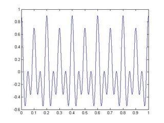
46 AIM: 9. FREQUENCY MODULATION To generate the waveform for frequency modulation using Matlab Simulation. THEORY: Frequency modulation uses the information signal, V m (t) to vary the carrier frequency within some small range about its original value. Here are the three signals in mathematical form Information: V m (t) Carrier: V c (t) = V co sin ( 2 π f c t + φ ) FM: V FM (t) = V co sin (2 π [f c + (Δf/V mo ) V m (t) ] t + φ) We have replaced the carrier frequency term, with a time-varying frequency. We have also introduced a new term: Δf, the peak frequency deviation. In this form, you should be able to see that the carrier frequency term: f c + (Δf/V mo ) V m (t) now varies between the extremes of f c - Δf and f c + Δf. The interpretation of Δf becomes clear: it is the farthest away from the original frequency that the FM signal can be. Sometimes it is referred to as the "swing" in the frequency. We can also define a modulation index for FM, analogous to AM: β = Δf/f m, where f m is the maximum modulating frequency used. The simplest interpretation of the modulation index, β, is as a measure of the peak frequency deviation, Δf. In other words, β represents a way to express the peak deviation frequency as a multiple of the maximum modulating frequency, f m, i.e. Δf = β f m. Example: suppose in FM radio that the audio signal to be transmitted ranges from 20 to 15,000 Hz (it does). If the FM system used a maximum modulating index, β, of 5.0, then the frequency would "swing" by a maximum of 5 x 15 khz = 75 khz above and below the carrier frequency. Here is a simple FM signal:
47 Here, the carrier is at 30 Hz, and the modulating frequency is 5 Hz. The modulation index is about 3, making the peak frequency deviation about 15 Hz. That means the frequency will vary somewhere between 15 and 45 Hz. How fast the cycle is completed is a function of the modulating frequency. PROGRAM: The frequency modulation (FM) waveform in time and frequency domain. fm=250hz,fc=5khz,vm=1v,vc=1v,m=10,t=0: : % setting vc=1; vm=1; fm=250; fc=5000; m=10; % x-axis: Time(second) t=0: : ; f=0:10:99990; % y-axis: Voltage(volt) wc=2*pi*fc; wm=2*pi*fm; sc_t=vc*cos(wc*t); sm_t=vm*cos(wm*t); kf=1000;
48 s_fm=vc*cos((wc*t)+10*sin(wm*t)); vf=abs(fft(s_fm,10^4))/5000; % Plot figure in time domain figure; plot(t,s_fm); hold on; plot(t,sm_t,'r'); axis([ ]); xlabel('time(second)'),ylabel('amplitude'); title('fm time-domain'); grid on; % Plot figure in frequency domain figure; plot(f,vf); axis([ 0 10^ ]); xlabel('frequency'), ylabel('amplitude'); title('fm frequency-domain'); grid on; %Plot modulating signal figure; plot(t,sm_t); axis([ ]); title('fm modulating signal'); RESULT: Thus the waveform for frequency Modulation is generated using Mat lab
GOVERNMENT OF KARNATAKA KARNATAKA STATE PRE-UNIVERSITY EDUCATION EXAMINATION BOARD II YEAR PUC EXAMINATION MARCH-2013 SCHEME OF VALUATION
 GOVERNMENT OF KARNATAKA KARNATAKA STATE PRE-UNIVERSITY EDUCATION EXAMINATION BOARD II YEAR PUC EXAMINATION MARCH-03 SCHEME OF VALUATION Subject Code: 0 Subject: PART - A 0. What does the arrow mark indicate
AC LAB ECE-D ecestudy.wordpress.com
 PART B EXPERIMENT NO: 1 AIM: PULSE AMPLITUDE MODULATION (PAM) & DEMODULATION DATE: To study Pulse Amplitude modulation and demodulation process with relevant waveforms. APPARATUS: 1. Pulse amplitude modulation
UNIVERSITY OF NORTH CAROLINA AT CHARLOTTE Department of Electrical and Computer Engineering
 UNIVERSITY OF NORTH CAROLINA AT CHARLOTTE Department of Electrical and Computer Engineering EXPERIMENT 8 AMPLITUDE MODULATION AND DEMODULATION OBJECTIVES The focus of this lab is to familiarize the student
Chapter 3. Question Mar No
 Chapter 3 Sr Question Mar No k. 1 Write any two drawbacks of TRF radio receiver 1. Instability due to oscillatory nature of RF amplifier.. Variation in bandwidth over tuning range. 3. Insufficient selectivity
DIGITAL COMMUNICATIONS LAB
 DIGITAL COMMUNICATIONS LAB List of Experiments: 1. PCM Generation and Detection. 2. Differential Pulse Code modulation. 3. Delta modulation. 4. Time Division Multiplexing of 2band Limited Signals. 5. Frequency
DEPARTMENT OF E.C.E.
 PVP SIDDHARTHA INSTITUTE OF TECHNOLOGY, KANURU, VIJAYAWADA-7 DEPARTMENT OF E.C.E. ANALOG COMMUNICATIONS LAB MANUAL Department of Electronics & Communication engineering Prasad V.Potluri Siddhartha Institute
Operating Manual Ver 1.1
 Frequency Modulation and Demodulation Trainer ST2203 Operating Manual Ver 1.1 An ISO 9001 : 2000 company 94-101, Electronic Complex Pardesipura, Indore- 452010, India Tel : 91-731- 2570301/02, 4211100
Wireless Communication
 Equipment and Instruments Wireless Communication An oscilloscope, a signal generator, an LCR-meter, electronic components (see the table below), a container for components, and a Scotch tape. Component
UNIT 2. Q.1) Describe the functioning of standard signal generator. Ans. Electronic Measurements & Instrumentation
 Describe the functioning of standard signal generator. Ans. Electronic Measurements & Instrumentation") UNIT 2 Q.1) Describe the functioning of standard signal generator Ans. STANDARD SIGNAL GENERATOR A standard signal generator produces known and controllable voltages. It is used as power source for the
UNIT 2 Q.1) Describe the functioning of standard signal generator Ans. STANDARD SIGNAL GENERATOR A standard signal generator produces known and controllable voltages. It is used as power source for the
B.Tech II Year II Semester (R13) Supplementary Examinations May/June 2017 ANALOG COMMUNICATION SYSTEMS (Electronics and Communication Engineering)
 Supplementary Examinations May/June 2017 ANALOG COMMUNICATION SYSTEMS (Electronics and Communication Engineering)") Code: 13A04404 R13 B.Tech II Year II Semester (R13) Supplementary Examinations May/June 2017 ANALOG COMMUNICATION SYSTEMS (Electronics and Communication Engineering) Time: 3 hours Max. Marks: 70 PART A
Code: 13A04404 R13 B.Tech II Year II Semester (R13) Supplementary Examinations May/June 2017 ANALOG COMMUNICATION SYSTEMS (Electronics and Communication Engineering) Time: 3 hours Max. Marks: 70 PART A
The steeper the phase shift as a function of frequency φ(ω) the more stable the frequency of oscillation
 the more stable the frequency of oscillation") It should be noted that the frequency of oscillation ω o is determined by the phase characteristics of the feedback loop. the loop oscillates at the frequency for which the phase is zero The steeper the
It should be noted that the frequency of oscillation ω o is determined by the phase characteristics of the feedback loop. the loop oscillates at the frequency for which the phase is zero The steeper the
Department of Electronics & Telecommunication Engg. LAB MANUAL. B.Tech V Semester [ ] (Branch: ETE)
![Department of Electronics & Telecommunication Engg. LAB MANUAL. B.Tech V Semester [ ] (Branch: ETE)](/thumbs/86/93078052.jpg "Department of Electronics & Telecommunication Engg. LAB MANUAL. B.Tech V Semester [ ] (Branch: ETE)") Department of Electronics & Telecommunication Engg. LAB MANUAL SUBJECT:-DIGITAL COMMUNICATION SYSTEM [BTEC-501] B.Tech V Semester [2013-14] (Branch: ETE) KCT COLLEGE OF ENGG & TECH., FATEHGARH PUNJAB TECHNICAL
Department of Electronics & Telecommunication Engg. LAB MANUAL SUBJECT:-DIGITAL COMMUNICATION SYSTEM [BTEC-501] B.Tech V Semester [2013-14] (Branch: ETE) KCT COLLEGE OF ENGG & TECH., FATEHGARH PUNJAB TECHNICAL
GOVERNMENT OF KARNATAKA KARNATAKA STATE PRE-UNIVERSITY EDUCATION EXAMINATION BOARD II YEAR PUC EXAMINATION MARCH-2012 SCHEME OF VALUATION
 GOVERNMENT OF KARNATAKA KARNATAKA STATE PRE-UNIVERSITY EDUCATION EXAMINATION BOARD II YEAR PUC EXAMINATION MARCH-0 SCHEME OF VALUATION Subject Code: 0 Subject: Qn. PART - A 0. Which is the largest of three
UNIT III ANALOG MULTIPLIER AND PLL
 UNIT III ANALOG MULTIPLIER AND PLL PART A (2 MARKS) 1. What are the advantages of variable transconductance technique? [AUC MAY 2012] Good Accuracy Economical Simple to integrate Reduced error Higher bandwidth
Code No: R Set No. 1
 Code No: R05220405 Set No. 1 II B.Tech II Semester Regular Examinations, Apr/May 2007 ANALOG COMMUNICATIONS ( Common to Electronics & Communication Engineering and Electronics & Telematics) Time: 3 hours
Shankersinh Vaghela Bapu Institute of Technology INDEX
 Shankersinh Vaghela Bapu Institute of Technology Diploma EE Semester III 3330905: ELECTRONIC COMPONENTS AND CIRCUITS INDEX Sr. No. Title Page Date Sign Grade 1 Obtain I-V characteristic of Diode. 2 To
EXPERIMENT 2.2 NON-LINEAR OP-AMP CIRCUITS
 2.16 EXPERIMENT 2.2 NONLINEAR OPAMP CIRCUITS 2.2.1 OBJECTIVE a. To study the operation of 741 opamp as comparator. b. To study the operation of active diode circuits (precisions circuits) using opamps,
Communication Systems Lab
 LAB MANUAL Communication Systems Lab (EE-226-F) Prepared by: Varun Sharma (Lab In-charge) Dayal C. Sati (Faculty In-charge) B R C M CET BAHAL DEPARTMENT OF ELECTRONICS & COMMUNICATION ENGINEERING Page
Amplitude Modulated Systems
 Amplitude Modulated Systems Communication is process of establishing connection between two points for information exchange. Channel refers to medium through which message travels e.g. wires, links, or
Electronic & Telecommunication Engineering
 Department of Electronic & Telecommunication Engineering LAB MANUAL Analog Communication System B.Tech IV Semester KCT College OF ENGG AND TECH. VILLAGE FATEHGARH DISTT.SANGRUR INDEX Sr.No: Experiments
Exercise 2: Demodulation (Quadrature Detector)
") Analog Communications Angle Modulation and Demodulation Exercise 2: Demodulation (Quadrature Detector) EXERCISE OBJECTIVE When you have completed this exercise, you will be able to explain demodulation
Analog Communications Angle Modulation and Demodulation Exercise 2: Demodulation (Quadrature Detector) EXERCISE OBJECTIVE When you have completed this exercise, you will be able to explain demodulation
Document Name: Electronic Circuits Lab. Facebook: Twitter:
 Document Name: Electronic Circuits Lab www.vidyathiplus.in Facebook: www.facebook.com/vidyarthiplus Twitter: www.twitter.com/vidyarthiplus Copyright 2011-2015 Vidyarthiplus.in (VP Group) Page 1 CIRCUIT
Emitter base bias. Collector base bias Active Forward Reverse Saturation forward Forward Cut off Reverse Reverse Inverse Reverse Forward
 SEMICONDUCTOR PHYSICS-2 [Transistor, constructional characteristics, biasing of transistors, transistor configuration, transistor as an amplifier, transistor as a switch, transistor as an oscillator] Transistor
Lab 4 : Transistor Oscillators
 Objective: Lab 4 : Transistor Oscillators In this lab, you will learn how to design and implement a colpitts oscillator. In part II you will implement a RC phase shift oscillator Hardware Required : Pre
Dev Bhoomi Institute Of Technology Department of Electronics and Communication Engineering PRACTICAL INSTRUCTION SHEET REV. NO. : REV.
 Dev Bhoomi Institute Of Technology Department of Electronics and Communication Engineering PRACTICAL INSTRUCTION SHEET LABORATORY MANUAL EXPERIMENT NO. ISSUE NO. : ISSUE DATE: July 200 REV. NO. : REV.
Summer 2015 Examination
 Summer 2015 Examination Subject Code: 17445 Model Answer Important Instructions to examiners: 1) The answers should be examined by key words and not as word-to-word as given in the model answer scheme.
EE-4022 Experiment 3 Frequency Modulation (FM)
") EE-4022 MILWAUKEE SCHOOL OF ENGINEERING 2015 Page 3-1 Student Objectives: EE-4022 Experiment 3 Frequency Modulation (FM) In this experiment the student will use laboratory modules including a Voltage-Controlled
EE-4022 MILWAUKEE SCHOOL OF ENGINEERING 2015 Page 3-1 Student Objectives: EE-4022 Experiment 3 Frequency Modulation (FM) In this experiment the student will use laboratory modules including a Voltage-Controlled
 UNIT I FUNDAMENTALS OF ANALOG COMMUNICATION Introduction In the Microbroadcasting services, a reliable radio communication system is of vital importance. The swiftly moving operations of modern communities
ET1210: Module 5 Inductance and Resonance
 Part 1 Inductors Theory: When current flows through a coil of wire, a magnetic field is created around the wire. This electromagnetic field accompanies any moving electric charge and is proportional to
Chapter 6. FM Circuits
 Chapter 6 FM Circuits Topics Covered 6-1: Frequency Modulators 6-2: Frequency Demodulators Objectives You should be able to: Explain the operation of an FM modulators and demodulators. Compare and contrast;
EXPERIMENT WISE VIVA QUESTIONS
 EXPERIMENT WISE VIVA QUESTIONS Pulse Code Modulation: 1. Draw the block diagram of basic digital communication system. How it is different from analog communication system. 2. What are the advantages of
State the application of negative feedback and positive feedback (one in each case)
") (ISO/IEC - 700-005 Certified) Subject Code: 073 Model wer Page No: / N Important Instructions to examiners: ) The answers should be examined by key words and not as word-to-word as given in the model answer
(ISO/IEC - 700-005 Certified) Subject Code: 073 Model wer Page No: / N Important Instructions to examiners: ) The answers should be examined by key words and not as word-to-word as given in the model answer
Time division multiplexing The block diagram for TDM is illustrated as shown in the figure
 CHAPTER 2 Syllabus: 1) Pulse amplitude modulation 2) TDM 3) Wave form coding techniques 4) PCM 5) Quantization noise and SNR 6) Robust quantization Pulse amplitude modulation In pulse amplitude modulation,
Laboratory Exercise 6 THE OSCILLOSCOPE
 Introduction Laboratory Exercise 6 THE OSCILLOSCOPE The aim of this exercise is to introduce you to the oscilloscope (often just called a scope), the most versatile and ubiquitous laboratory measuring
LIC & COMMUNICATION LAB MANUAL
 LIC & Communication Lab Manual LIC & COMMUNICATION LAB MANUAL FOR V SEMESTER B.E (E& ( E&C) (For private circulation only) NAME: DEPARTMENT OF ELECTRONICS & COMMUNICATION SRI SIDDHARTHA INSTITUTE OF TECHNOLOGY
Lecture 6. Angle Modulation and Demodulation
 Lecture 6 and Demodulation Agenda Introduction to and Demodulation Frequency and Phase Modulation Angle Demodulation FM Applications Introduction The other two parameters (frequency and phase) of the carrier
Week 8 AM Modulation and the AM Receiver
 Week 8 AM Modulation and the AM Receiver The concept of modulation and radio transmission is introduced. An AM receiver is studied and the constructed on the prototyping board. The operation of the AM
An induced emf is the negative of a changing magnetic field. Similarly, a self-induced emf would be found by
 This is a study guide for Exam 4. You are expected to understand and be able to answer mathematical questions on the following topics. Chapter 32 Self-Induction and Induction While a battery creates an
Analog and Telecommunication Electronics
 Politecnico di Torino Electronic Eng. Master Degree Analog and Telecommunication Electronics C5 - Synchronous demodulation» AM and FM demodulation» Coherent demodulation» Tone decoders AY 2015-16 19/03/2016-1
VALLIAMMAI ENGINEERING COLLEGE
 VALLIAMMAI ENGINEERING COLLEGE SRM Nagar, Kattankulathur 603 203. DEPARTMENT OF ELECTRONICS & COMMUNICATION ENGINEERING SUBJECT QUESTION BANK : EC6401 ELECTRONICS CIRCUITS-II SEM / YEAR: IV / II year B.E.
TUNED AMPLIFIERS 5.1 Introduction: Coil Losses:
 TUNED AMPLIFIERS 5.1 Introduction: To amplify the selective range of frequencies, the resistive load R C is replaced by a tuned circuit. The tuned circuit is capable of amplifying a signal over a narrow
LINEAR IC APPLICATIONS
 1 B.Tech III Year I Semester (R09) Regular & Supplementary Examinations December/January 2013/14 1 (a) Why is R e in an emitter-coupled differential amplifier replaced by a constant current source? (b)
GOVERNMENT OF KARNATAKA KARNATAKA STATE PRE-UNIVERSITY EDUCATION EXAMINATION BOARD II YEAR PUC EXAMINATION JULY-2012 SCHEME OF VALUATION
 GOVERNMENT OF KARNATAKA KARNATAKA STATE PRE-UNIVERSITY EDUCATION EXAMINATION BOARD II YEAR PUC EXAMINATION JULY-0 SCHEME OF VALUATION Subject Code: 40 Subject: PART - A 0. Which region of the transistor
Power Line Carrier Communication
 IOSR Journal of Electronics and Communication Engineering (IOSR-JECE) e-issn: 2278-2834,p- ISSN: 2278-8735.Volume 9, Issue 2, Ver. II (Mar - Apr. 2014), PP 50-55 Power Line Carrier Communication Dorathe.
Jawaharlal Nehru Engineering College
 Jawaharlal Nehru Engineering College Laboratory Manual COMMUNICATION ENGINEERING For Author JNEC, Aurangabad. Second Year Students Lab manual made by PROF. S.A. ANNANDATE PROF. P. B. MURMUDE PROF. P.B.YADAV
DIGITAL ELECTRONICS WAVE SHAPING AND PULSE CIRCUITS. September 2012
 AM 5-403 DIGITAL ELECTRONICS WAVE SHAPING AND PULSE CIRCUITS September 2012 DISTRIBUTION RESTRICTION: Approved for public release. Distribution is unlimited. DEPARTMENT OF THE ARMY MILITARY AUXILIARY RADIO
B.E. SEMESTER III (ELECTRICAL) SUBJECT CODE: X30902 Subject Name: Analog & Digital Electronics
 SUBJECT CODE: X30902 Subject Name: Analog & Digital Electronics") B.E. SEMESTER III (ELECTRICAL) SUBJECT CODE: X30902 Subject Name: Analog & Digital Electronics Sr. No. Date TITLE To From Marks Sign 1 To verify the application of op-amp as an Inverting Amplifier 2 To
B.E. SEMESTER III (ELECTRICAL) SUBJECT CODE: X30902 Subject Name: Analog & Digital Electronics Sr. No. Date TITLE To From Marks Sign 1 To verify the application of op-amp as an Inverting Amplifier 2 To
Communication Circuit Lab Manual
 German Jordanian University School of Electrical Engineering and IT Department of Electrical and Communication Engineering Communication Circuit Lab Manual Experiment 2 Tuned Amplifier Eng. Anas Alashqar
SEM: V EXAM MARKS: 50 BRANCH: EC IA MARKS: 25 SUBJECT: ANALOG COMMUNICATION & LIC LAB SUB CODE: 06ECL58
 LIST OF EXPERIMENTS SEM: V EXAM MARKS: 50 BRANCH: EC IA MARKS: 25 SUBJECT: ANALOG COMMUNICATION & LIC LAB SUB CODE: 06ECL58 1) Active low pass & high pass filters second order 2) Active band pass & band
Shankersinh Vaghela Bapu Institute of Technology
 Shankersinh Vaghela Bapu Institute of Technology B.E. Semester III (EC) 131101: Basic Electronics INDEX Sr. No. Title Page Date Sign Grade 1 [A] To Study the V-I characteristic of PN junction diode. [B]
EXPT NO: 1.A. COMMON EMITTER AMPLIFIER (Software) PRELAB:
 PRELAB:") EXPT NO: 1.A COMMON EMITTER AMPLIFIER (Software) PRELAB: 1. Study the operation and working principle of CE amplifier. 2. Identify all the formulae you will need in this Lab. 3. Study the procedure of
EXPT NO: 1.A COMMON EMITTER AMPLIFIER (Software) PRELAB: 1. Study the operation and working principle of CE amplifier. 2. Identify all the formulae you will need in this Lab. 3. Study the procedure of
Speech, music, images, and video are examples of analog signals. Each of these signals is characterized by its bandwidth, dynamic range, and the
 Speech, music, images, and video are examples of analog signals. Each of these signals is characterized by its bandwidth, dynamic range, and the nature of the signal. For instance, in the case of audio
Exam Booklet. Pulse Circuits
 Exam Booklet Pulse Circuits Pulse Circuits STUDY ASSIGNMENT This booklet contains two examinations for the six lessons entitled Pulse Circuits. The material is intended to provide the last training sought
ELECTRONIC CIRCUITS LAB
 ELECTRONIC CIRCUITS LAB 1 2 STATE INSTITUTE OF TECHNICAL TEACHERS TRAINING AND RESEARCH GENERAL INSTRUCTIONS Rough record and Fair record are needed to record the experiments conducted in the laboratory.
EE12: Laboratory Project (Part-2) AM Transmitter
 AM Transmitter") EE12: Laboratory Project (Part-2) AM Transmitter ECE Department, Tufts University Spring 2008 1 Objective This laboratory exercise is the second part of the EE12 project of building an AM transmitter in
EE12: Laboratory Project (Part-2) AM Transmitter ECE Department, Tufts University Spring 2008 1 Objective This laboratory exercise is the second part of the EE12 project of building an AM transmitter in
Communication Circuit Lab Manual
 German Jordanian University School of Electrical Engineering and IT Department of Electrical and Communication Engineering Communication Circuit Lab Manual Experiment 3 Crystal Oscillator Eng. Anas Alashqar
Testing and Stabilizing Feedback Loops in Today s Power Supplies
 Keywords Venable, frequency response analyzer, impedance, injection transformer, oscillator, feedback loop, Bode Plot, power supply design, open loop transfer function, voltage loop gain, error amplifier,
1) Consider the circuit shown in figure below. Compute the output waveform for an input of 5kHz
 Consider the circuit shown in figure below. Compute the output waveform for an input of 5kHz") ) Consider the circuit shown in figure below. Compute the output waveform for an input of 5kHz Solution: a) Input is of constant amplitude of 2 V from 0 to 0. ms and 2 V from 0. ms to 0.2 ms. The output
) Consider the circuit shown in figure below. Compute the output waveform for an input of 5kHz Solution: a) Input is of constant amplitude of 2 V from 0 to 0. ms and 2 V from 0. ms to 0.2 ms. The output
MAHALAKSHMI ENGINEERING COLLEGE TIRUCHIRAPALLI UNIT III TUNED AMPLIFIERS PART A (2 Marks)
") MAHALAKSHMI ENGINEERING COLLEGE TIRUCHIRAPALLI-621213. UNIT III TUNED AMPLIFIERS PART A (2 Marks) 1. What is meant by tuned amplifiers? Tuned amplifiers are amplifiers that are designed to reject a certain
MAHALAKSHMI ENGINEERING COLLEGE TIRUCHIRAPALLI-621213. UNIT III TUNED AMPLIFIERS PART A (2 Marks) 1. What is meant by tuned amplifiers? Tuned amplifiers are amplifiers that are designed to reject a certain
An active filter offers the following advantages over a passive filter:
 ACTIVE FILTERS An electric filter is often a frequency-selective circuit that passes a specified band of frequencies and blocks or attenuates signals of frequencies outside this band. Filters may be classified
ANALOG COMMUNICATION
 ANALOG COMMUNICATION TRAINING LAB Analog Communication Training Lab consists of six kits, one each for Modulation (ACL-01), Demodulation (ACL-02), Modulation (ACL-03), Demodulation (ACL-04), Noise power
COMMUNICATIONS LAB. Duration of University Examination University Examination
 COMMUNICATIONS LAB Instructions Duration of University Examination University Examination Sessional 4 Periods per week 3 Hours 50 Marks 25 Marks Course Objectives: 1. Demonstrate AM, FM, Mixer, PAM, PWM
Figure 1: Closed Loop System
 SIGNAL GENERATORS 3. Introduction Signal sources have a variety of applications including checking stage gain, frequency response, and alignment in receivers and in a wide range of other electronics equipment.
Lab 2: Common Base Common Collector Design Exercise
 CSUS EEE 109 Lab - Section 01 Lab 2: Common Base Common Collector Design Exercise Author: Bogdan Pishtoy / Lab Partner: Roman Vermenchuk Lab Report due March 26 th Lab Instructor: Dr. Kevin Geoghegan 2016-03-25
Low Pass Filter Introduction
 Low Pass Filter Introduction Basically, an electrical filter is a circuit that can be designed to modify, reshape or reject all unwanted frequencies of an electrical signal and accept or pass only those
Dev Bhoomi Institute Of Technology Department of Electronics and Communication Engineering PRACTICAL INSTRUCTION SHEET
 Dev Bhoomi Institute Of Technology Department of Electronics and Communication Engineering PRACTICAL INSTRUCTION SHEET LABORATORY MANUAL EXPERIMENT NO. ISSUE NO. : ISSUE DATE: REV. NO. : REV. DATE : PAGE:
LENDI INSTITUTE OF ENGINEERING & TECHNOLOGY
 LENDI INSTITUTE OF ENGINEERING & TECHNOLOGY (Approved by A.I.C.T.E & Affiliated to JNTU,Kakinada) Jonnada (Village), Denkada (Mandal), Vizianagaram Dist 535 005 Phone No. 08922-241111, 241112 E-Mail: lendi_2008@yahoo.com
Exercise 1: RF Stage, Mixer, and IF Filter
 SSB Reception Analog Communications Exercise 1: RF Stage, Mixer, and IF Filter EXERCISE OBJECTIVE DISCUSSION On the circuit board, you will set up the SSB transmitter to transmit a 1000 khz SSB signal
CHAPTER 2! AMPLITUDE MODULATION (AM)
") CHAPTER 2 AMPLITUDE MODULATION (AM) Topics 2-1 : AM Concepts 2-2 : Modulation Index and Percentage of Modulation 2-3 : Sidebands and the Frequency Domain 2-4 : Single-Sideband Modulation 2-5 : AM Power
CHAPTER 2 AMPLITUDE MODULATION (AM) Topics 2-1 : AM Concepts 2-2 : Modulation Index and Percentage of Modulation 2-3 : Sidebands and the Frequency Domain 2-4 : Single-Sideband Modulation 2-5 : AM Power
Oscillators. An oscillator may be described as a source of alternating voltage. It is different than amplifier.
 Oscillators An oscillator may be described as a source of alternating voltage. It is different than amplifier. An amplifier delivers an output signal whose waveform corresponds to the input signal but
Navy Electricity and Electronics Training Series
 NONRESIDENT TRAINING COURSE SEPTEMBER 1998 Navy Electricity and Electronics Training Series Module 9 Introduction to Wave- Generation and Wave-Shaping NAVEDTRA 14181 DISTRIBUTION STATEMENT A: Approved
Difference between BJTs and FETs. Junction Field Effect Transistors (JFET)
") Difference between BJTs and FETs Transistors can be categorized according to their structure, and two of the more commonly known transistor structures, are the BJT and FET. The comparison between BJTs
Difference between BJTs and FETs Transistors can be categorized according to their structure, and two of the more commonly known transistor structures, are the BJT and FET. The comparison between BJTs
TDA7000 for narrowband FM reception
 TDA7 for narrowband FM reception Author: Author: W.V. Dooremolen INTRODUCTION Today s cordless telephone sets make use of duplex communication with carrier frequencies of about.7mhz and 49MHz. In the base
List of Figures. Sr. no.
 List of Figures Sr. no. Topic No. Topic 1 1.3.1 Angle Modulation Graphs 11 2 2.1 Resistor 13 3 3.1 Block Diagram of The FM Transmitter 15 4 4.2 Basic Diagram of FM Transmitter 17 5 4.3 Circuit Diagram
DC and AC Circuits. Objective. Theory. 1. Direct Current (DC) R-C Circuit
 R-C Circuit") [International Campus Lab] Objective Determine the behavior of resistors, capacitors, and inductors in DC and AC circuits. Theory ----------------------------- Reference -------------------------- Young
[International Campus Lab] Objective Determine the behavior of resistors, capacitors, and inductors in DC and AC circuits. Theory ----------------------------- Reference -------------------------- Young
Chapter 33. Alternating Current Circuits
 Chapter 33 Alternating Current Circuits Alternating Current Circuits Electrical appliances in the house use alternating current (AC) circuits. If an AC source applies an alternating voltage to a series
Table of Contents Lesson One Lesson Two Lesson Three Lesson Four Lesson Five PREVIEW COPY
 Oscillators Table of Contents Lesson One Lesson Two Lesson Three Introduction to Oscillators...3 Flip-Flops...19 Logic Clocks...37 Lesson Four Filters and Waveforms...53 Lesson Five Troubleshooting Oscillators...69
Experiment 7: Frequency Modulation and Phase Locked Loops
 Experiment 7: Frequency Modulation and Phase Locked Loops Frequency Modulation Background Normally, we consider a voltage wave form with a fixed frequency of the form v(t) = V sin( ct + ), (1) where c
ANALOG ELECTRONIC CIRCUITS LABORATORY MANUAL (CODE: EEE - 228)
") ANALOG ELECTRONIC CIRCUITS LABORATORY MANUAL (CODE: EEE - 228) DEPARTMENT OF ELECTRONICS & COMMUNICATION ENGINEERING ANIL NEERUKONDA INSTITUTE OF TECHNOLOGY & SCIENCES (Affiliated to AU, Approved by AICTE
ANALOG ELECTRONIC CIRCUITS LABORATORY MANUAL (CODE: EEE - 228) DEPARTMENT OF ELECTRONICS & COMMUNICATION ENGINEERING ANIL NEERUKONDA INSTITUTE OF TECHNOLOGY & SCIENCES (Affiliated to AU, Approved by AICTE
SIR PADAMPAT SINGHANIA UNIVERSITY UDAIPUR Sample Question Paper for Ph.D. (Electronics & Communication Engineering) SPSAT 18
 SPSAT 18") INSTRUCTIONS SIR PADAMPAT SINGHANIA UNIVERSITY UDAIPUR Sample Question Paper for Ph.D. (Electronics & Communication Engineering) SPSAT 18 The test is 60 minutes long and consists of 40 multiple choice
INSTRUCTIONS SIR PADAMPAT SINGHANIA UNIVERSITY UDAIPUR Sample Question Paper for Ph.D. (Electronics & Communication Engineering) SPSAT 18 The test is 60 minutes long and consists of 40 multiple choice
Testing Power Sources for Stability
 Keywords Venable, frequency response analyzer, oscillator, power source, stability testing, feedback loop, error amplifier compensation, impedance, output voltage, transfer function, gain crossover, bode
LBI-30398N. MAINTENANCE MANUAL MHz PHASE LOCK LOOP EXCITER 19D423249G1 & G2 DESCRIPTION TABLE OF CONTENTS. Page. DESCRIPTION...
 MAINTENANCE MANUAL 138-174 MHz PHASE LOCK LOOP EXCITER 19D423249G1 & G2 LBI-30398N TABLE OF CONTENTS DESCRIPTION...Front Cover CIRCUIT ANALYSIS... 1 MODIFICATION INSTRUCTIONS... 4 PARTS LIST AND PRODUCTION
THIRD SEMESTER DIPLOMA EXAMINATION IN ELECTRICAL & ELECTRONICS ENGINEERING, MARCH 2013 ELECTRONIC DEVICES AND CIRCUITS
 REVISION-2010 Reg. No SUB CODE:3053 Signature THIRD SEMESTER DIPLOMA EXAMINATION IN ELECTRICAL & ELECTRONICS ENGINEERING, MARCH 2013 ELECTRONIC DEVICES AND CIRCUITS Time :3hours Maximum marks:100 PART
DESIGN OF CMOS BASED FM QUADRATURE DEMODULATOR USING 45NM TECHNOLOGY
 DESIGN OF CMOS BASED FM QUADRATURE DEMODULATOR USING 45NM TECHNOLOGY 1 Pardeep Kumar, 2 Rekha Yadav, 1, 2 Electronics and Communication Engineering Department D.C.R.U.S.T. Murthal, 1, 2 Sonepat, 1, 2 Haryana,
EE POWER ELECTRONICS UNIT IV INVERTERS
 EE6503 - POWER ELECTRONICS UNIT IV INVERTERS PART- A 1. Define harmonic distortion factor? (N/D15) Harmonic distortion factor is the harmonic voltage to the fundamental voltage. 2. What is CSI? (N/D12)
Sampling and Reconstruction
 Experiment 10 Sampling and Reconstruction In this experiment we shall learn how an analog signal can be sampled in the time domain and then how the same samples can be used to reconstruct the original
FDM- FREQUENCY DIVISION MULTIPLEXING
 FDM- FREQUENCY DIVISION MULTIPLEXING Multiplexing to refer to the combination of information streams from multiple sources for transmission over a shared medium Demultiplexing to refer to the separation
Analog Communication.
 Analog Communication Vishnu N V Tele is Greek for at a distance, and Communicare is latin for to make common. Telecommunication is the process of long distance communications. Early telecommunications
For input: Peak to peak amplitude of the input = volts. Time period for 1 full cycle = sec
 Inverting amplifier: [Closed Loop Configuration] Design: A CL = V o /V in = - R f / R in ; Assume R in = ; Gain = ; Circuit Diagram: RF +10V F.G ~ + Rin 2 3 7 IC741 + 4 6 v0-10v CRO Model Graph Inverting
Department of Electronics & Communication Engineering LAB MANUAL SUBJECT: DIGITAL COMMUNICATION LABORATORY [ECE324] (Branch: ECE)
![Department of Electronics & Communication Engineering LAB MANUAL SUBJECT: DIGITAL COMMUNICATION LABORATORY [ECE324] (Branch: ECE)](/thumbs/96/127341232.jpg "Department of Electronics & Communication Engineering LAB MANUAL SUBJECT: DIGITAL COMMUNICATION LABORATORY [ECE324] (Branch: ECE)") Department of Electronics & Communication Engineering LAB MANUAL SUBJECT: DIGITAL COMMUNICATION LABORATORY [ECE324] B.Tech Year 3 rd, Semester - 5 th (Branch: ECE) Version: 01 st August 2018 The LNM Institute
Department of Electronics & Communication Engineering LAB MANUAL SUBJECT: DIGITAL COMMUNICATION LABORATORY [ECE324] B.Tech Year 3 rd, Semester - 5 th (Branch: ECE) Version: 01 st August 2018 The LNM Institute
 EC 6411 CIRCUITS AND SIMULATION INTEGRATED LABORATORY LABORATORY MANUAL INDEX EXPT.NO NAME OF THE EXPERIMENT PAGE NO 1 HALF WAVE AND FULL WAVE RECTIFIER 3 2 FIXED BIAS AMPLIFIER CIRCUIT USING BJT 3 BJT
LM13600 Dual Operational Transconductance Amplifiers with Linearizing Diodes and Buffers
 LM13600 Dual Operational Transconductance Amplifiers with Linearizing Diodes and Buffers General Description The LM13600 series consists of two current controlled transconductance amplifiers each with
CME 312-Lab Communication Systems Laboratory
 Objective: By the end of this experiment, the student should be able to: 1. Demonstrate the Modulation and Demodulation of the AM. 2. Observe the relation between modulation index and AM signal envelope.
AM Generation High Level Low Level
 AM Generation High Level Low Level Low-level generation In modern radio systems, modulated signals are generated via digital signal processing (DSP). With DSP many types of AM modulation are possible with
AM in frequency domain ( 1 M)
") 1) The Answer should be examined by key words and not as word-to-word as given in the Model Answer scheme. 2) The model Answer and the Answer written by candidate may vary but the examiner may try to assess
1) The Answer should be examined by key words and not as word-to-word as given in the Model Answer scheme. 2) The model Answer and the Answer written by candidate may vary but the examiner may try to assess
Resonance. A resonant circuit (series or parallel) must have an inductive and a capacitive element.
 must have an inductive and a capacitive element.") 1. Series Resonant: Resonance A resonant circuit (series or parallel) must have an inductive and a capacitive element. The total impedance of this network is: The circuit will reach its maximum Voltage
1. Series Resonant: Resonance A resonant circuit (series or parallel) must have an inductive and a capacitive element. The total impedance of this network is: The circuit will reach its maximum Voltage
ERICSSONZ LBI-30398P. MAINTENANCE MANUAL MHz PHASE LOCKED LOOP EXCITER 19D423249G1 & G2 DESCRIPTION TABLE OF CONTENTS
 MAINTENANCE MANUAL 138-174 MHz PHASE LOCKED LOOP EXCITER 19D423249G1 & G2 TABLE OF CONTENTS Page DESCRIPTION... Front Cover CIRCUIT ANALYSIS...1 MODIFICATION INSTRUCTIONS...4 PARTS LIST...5 PRODUCTION
CHAPTER 1 DIODE CIRCUITS. Semiconductor act differently to DC and AC currents
 CHAPTER 1 DIODE CIRCUITS Resistance levels Semiconductor act differently to DC and AC currents There are three types of resistances 1. DC or static resistance The application of DC voltage to a circuit
NOORUL ISLAM COLLEGE OF ENGG, KUMARACOIL. DEPARTMENT OF ELECTRONICS AND COMMUNICATION ENGG. SUBJECT CODE: EC 1251 SUBJECT NAME: ELECTRONIC CIRCUITS-II
 NOORUL ISLAM COLLEGE OF ENGG, KUMARACOIL. DEPARTMENT OF ELECTRONICS AND COMMUNICATION ENGG. SUBJECT CODE: EC 1251 SUBJECT NAME: ELECTRONIC CIRCUITS-II Prepared by, C.P.SREE BALA LEKSHMI (Lect/ECE) ELECTRONICS
Series and Parallel Resonant Circuits
 Series and Parallel Resonant Circuits Aim: To obtain the characteristics of series and parallel resonant circuits. Apparatus required: Decade resistance box, Decade inductance box, Decade capacitance box