Emona DATEx. Volume 2 Further Experiments in Modern Analog & Digital Telecommunications For NI ELVIS I and II. Barry Duncan
|
|
|
- Leo Horn
- 5 years ago
- Views:
Transcription
1 Emona DATEx Lab Manual Volume 2 Further Experiments in Modern Analog & Digital Telecommunications For NI ELVIS I and II Barry Duncan
2 .
3 Emona DATEx Lab Manual Volume 2 Further Experiments in Modern Analog & Digital Telecommunications For NI ELVIS I and II Barry Duncan
4 Emona DATEx Lab Manual for NI ELVIS I and II Volume 2 - Further Experiments in Modern Analog and Digital Telecommunications. Author: Barry Duncan Technical editor: Carlo Manfredini Issue Number: Vol2 issue 1.1 Published by: Emona Instruments Pty Ltd, 78 Parramatta Road Camperdown NSW 2050 AUSTRALIA. web: telephone: fax: Copyright Emona Instruments Pty Ltd and its related entities. All rights reserved. No part of this publication may be reproduced, translated, adapted, modified, edited or distributed in any form or by any means, including any network or Web distribution or broadcast for distance learning, or stored in any database or in any network retrieval system, without the prior written consent of Emona Instruments Pty Ltd. For licensing information, please contact Emona Instruments Pty Ltd. DATEx is a trademark of Emona TIMS Pty Ltd. LabVIEW, National Instruments, NI, NI ELVIS, and NI-DAQ are trademarks of National Instruments Corporation. Product and company names mentioned herein are trademarks or trade names of their respective companies. Printed in Australia
5 Contents Introduction... i - iv 1 - AM (method 2) and product detection of AM signals... Expt Noise in AM communications... Expt PCM and time division multiplexing (TDM)... Expt An introduction to Armstrong s modulator... Expt Phase division modulation and demodulation... Expt Pulse-width modulation and demodulation... Expt Message translation and inversion... Expt Carrier acquisition using the phase-locked loop... Expt Signal-to-noise ratio and eye diagrams... Expt Pulse code modulation and signal-to-noise distortion ratio (SNDR) Expt ASK demodulation using product detection... Expt FSK generation (switching method) and demodulation... Expt Principles of Gaussian FSK (GFSK)... Expt PN sequence spectra and noise generation... Expt Line coding and bit-clock regeneration... Expt Delta modulation and demodulation... Expt Delta-sigma modulation and demodulation... Expt FM Generation using the harmonic multiplier method... Expt 18-1
6
7 i
8
9 iii
10
11
12
13
14
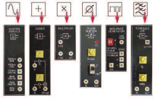
15 MASTER SIGNALS SINE COS 8kHz SINE MULTIPLIER DC Y AC kxy MULTIPLIER X DC Y DC DC X AC kxy SCOPE 10VDC 7Vrms max CH 0 CH 1
16
17 Y DC AC MULTIPLIER MULTIPLIER kxy X DC Y DC kxy DC X AC MASTER SIGNALS SINE COS 8kHz SINE CH 0 CH 1 SCOPE 10VDC 7Vrms max B A ADDER G GA+gB g IN OUT 0 O 180 O PHASE PHASE SHIFTER LO
18
19
20 V LSB USB LSB Carrier USB f Carrier
21
22
23 MASTER SIGNALS MULTIPLIER DC X AC PHASE SHIFTER LO ADDER SCOPE 10VDC 7Vrms max CH 0 SINE COS 8kHz SINE DC Y AC kxy MULTIPLIER X DC Y DC kxy PHASE 0 O 180 O IN OUT A B G g GA+gB CH 1
24
25 MASTER SIGNALS MULTIPLIER DC X AC PHASE SHIFTER LO ADDER UTILITIES COMPARATOR REF SCOPE 10VDC 7Vrms max CH 0 SINE COS 8kHz SINE DC Y AC kxy MULTIPLIER X DC Y DC kxy PHASE 0 O 180 O IN OUT A B G g GA+gB IN OUT RECTIFIER DIODE & RC LPF RC LPF CH 1
26
27
28
29
30 = = = + =
31
32
33 MASTER SIGNALS FUNCTION GENERATOR ADDER MULTIPLIER SINE COS 8kHz SINE ANALOG I/ O ACH1 DAC1 ACH0 DAC0 VARIABLE DC + A B G g GA+gB DC Y AC kxy MULTIPLIER X DC Y DC DC X AC kxy SCOPE 10VDC 7Vrms max CH 0 CH 1
34
35 MASTER SIGNALS FUNCTION GENERATOR ADDER MULTIPLIER SINE COS 8kHz SINE ANALOG I/ O ACH1 DAC1 ACH0 DAC0 VARIABLE DC + A B G g GA+gB DC Y AC kxy MULTIPLIER X DC Y DC DC X AC kxy SCOPE 10VDC 7Vrms max CH 0 CH 1 NOISE GENERATOR 0dB -6dB -20dB AMPLIFIER CHANNEL MODULE CHANNEL BPF BASEBAND LPF ADDER UTILITIES COMPARATOR REF IN OUT RECTIFIER GAIN NOISE DIODE & RC LPF IN OUT SIGNAL CHANNEL OUT RC LPF
36
37 MASTER SIGNALS FUNCTION GENERATOR ADDER MULTIPLIER SINE COS 8kHz SINE ANALOG I/ O ACH1 DAC1 ACH0 DAC0 VARIABLE DC + A B G g GA+gB DC Y AC kxy MULTIPLIER X DC Y DC DC X AC kxy SCOPE 10VDC 7Vrms max CH 0 CH 1 NOISE GENERATOR 0dB -6dB -20dB AMPLIFIER CHANNEL MODULE CHANNEL BPF BASEBAND LPF ADDER UTILITIES COMPARATOR REF IN OUT RECTIFIER GAIN NOISE DIODE & RC LPF IN OUT SIGNAL CHANNEL OUT RC LPF
38
39 + =
40
41 MASTER SIGNALS FUNCTION GENERATOR ADDER MULTIPLIER SINE COS 8kHz SINE ANALOG I/ O ACH1 DAC1 ACH0 DAC0 VARIABLE DC + A B G g GA+gB DC Y AC kxy MULTIPLIER X DC Y DC DC X AC kxy SCOPE 10VDC 7Vrms max CH 0 CH 1
42 MASTER SIGNALS FUNCTION GENERATOR ADDER MULTIPLIER SINE COS 8kHz SINE ANALOG I/ O ACH1 DAC1 ACH0 DAC0 VARIABLE DC + A B G g GA+gB DC Y AC kxy MULTIPLIER X DC Y DC DC X AC kxy SCOPE 10VDC 7Vrms max CH 0 CH 1 NOISE GENERATOR CHANNEL MODULE MULTIPLIER UTILITIES COMPARATOR REF 0dB -6dB CHANNEL BPF X DC -20dB AMPLIFIER GAIN NOISE BASEBAND LPF ADDER Y DC kxy SERIAL TO PARALLEL S/ P IN OUT RECTIFIER DIODE & RC LPF IN OUT SIGNAL CHANNEL OUT SERIAL X1 RC LPF CLK X2
43
44 MASTER SIGNALS FUNCTION GENERATOR ADDER MULTIPLIER SINE COS 8kHz SINE ANALOG I/ O ACH1 DAC1 ACH0 DAC0 VARIABLE DC + A B G g GA+gB DC Y AC kxy MULTIPLIER X DC Y DC DC X AC kxy SCOPE 10VDC 7Vrms max CH 0 CH 1 NOISE GENERATOR CHANNEL MODULE MULTIPLIER UTILITIES COMPARATOR REF 0dB -6dB CHANNEL BPF X DC -20dB AMPLIFIER GAIN NOISE BASEBAND LPF ADDER Y DC kxy SERIAL TO PARALLEL S/ P IN OUT RECTIFIER DIODE & RC LPF IN OUT SIGNAL CHANNEL OUT SERIAL X1 RC LPF CLK X2
45
46 + =
47
48
49
50
51
52
53 FUNCTION GENERATOR MASTER SIGNALS PCM ENCODER PCM DECODER TUNEABLE LPF GND ANALOG I/ O ACH1 DAC1 SINE COS PCM TDM INPUT 2 FS FS TDM f C x100 f C SCOPE 10VDC 7Vrms max CH 0 ACH0 DAC0 VARIABLE DC + 8kHz SINE INPUT 1 CLK PCM DATA PCM DATA CLK OUTPUT2 OUTPUT GAIN CH 1 IN OUT
54
55
56
57
58
59 FUNCTION GENERATOR MASTER SIGNALS PCM ENCODER PCM DECODER TUNEABLE LPF GND ANALOG I/ O ACH1 DAC1 SINE COS PCM TDM INPUT 2 FS FS TDM f C x100 f C SCOPE 10VDC 7Vrms max CH 0 ACH0 DAC0 VARIABLE DC + 8kHz SINE INPUT 1 CLK PCM DATA PCM DATA CLK OUTPUT2 OUTPUT GAIN CH 1 IN OUT
60 PCM ENCODER FS CLK PCM DATA TDM INPUT 2 INPUT 1 PCM MASTER SIGNALS SINE COS 8kHz SINE PCM DECODER FS PCM DATA CLK OUTPUT TDM OUTPUT2 GND f C x100 f C GAIN IN OUT TUNEABLE LPF VARIABLE DC FUNCTION GENERATOR + ANALOG I/ O ACH1 DAC1 ACH0 DAC0 AMPLIFIER GAIN OUT IN 0dB -6dB -20dB NOISE GENERATOR
61 MASTER SIGNALS PCM ENCODER PCM DECODER TUNEABLE LPF NOISE GENERATOR GND 0dB PCM TDM TDM f C x100-6db -20dB SINE COS 8kHz SINE INPUT 2 INPUT 1 CLK FS PCM DATA FS PCM DATA CLK OUTPUT2 OUTPUT f C GAIN IN OUT AMPLIFIER GAIN IN OUT SEQUENCE GENERATOR O 1 OO NRZ-L SYNC O1 Bi-O 1O RZ-AMI 11 NRZ-M X LINE CODE CHANNEL MODULE CHANNEL BPF BASEBAND LPF CLK Y SPEECH NOISE ADDER GND GND SIGNAL CHANNEL OUT
62
63
64
65 θ θ
66 θ θ
67 MASTER SIGNALS SINE COS 8kHz SINE MULTIPLIER DC Y AC kxy MULTIPLIER X DC Y DC DC X AC kxy SCOPE 10VDC 7Vrms max CH 0 CH 1
68
69 MASTER SIGNALS MULTIPLIER DC X AC PHASE SHIFTER LO ADDER SCOPE 10VDC 7Vrms max CH 0 SINE COS 8kHz SINE DC Y AC kxy MULTIPLIER X DC Y DC kxy PHASE 0 O 180 O IN OUT A B G g GA+gB CH 1
70
71
72
73 MASTER SIGNALS MULTIPLIER PHASE SHIFTER ADDER UTILITIES COMPARATOR REF NOISE GENERATOR DC X AC LO 0dB -6dB SINE COS 8kHz SINE DC Y AC kxy MULTIPLIER X DC Y DC kxy PHASE 0 O 180 O IN OUT A B G g GA+gB IN OUT RECTIFIER DIODE & RC LPF RC LPF -20dB AMPLIFIER GAIN IN OUT
74 MASTER SIGNALS MULTIPLIER DC X AC PHASE SHIFTER LO ADDER SCOPE 10VDC 7Vrms max CH 0 SINE COS 8kHz SINE DC Y AC kxy MULTIPLIER X DC Y DC kxy PHASE 0 O 180 O IN OUT A B G g GA+gB CH 1 UTILITIES COMPARATOR REF CHANNEL MODULE CHANNEL BPF GND IN OUT RECTIFIER DIODE & RC LPF NOISE BASEBAND LPF ADDER RC LPF SIGNAL CHANNEL OUT
75
76
77
78 Π
79 Π
80
81 FUNCTION GENERATOR MASTER SIGNALS MULTIPLIER ANALOG I/ O ACH1 DAC1 ACH0 DAC0 VARIABLE DC + SINE COS 8kHz SINE DC Y AC kxy MULTIPLIER X DC Y DC DC X AC kxy SCOPE 10VDC 7Vrms max CH 0 CH 1
82
83 FUNCTION GENERATOR MASTER SIGNALS MULTIPLIER ANALOG I/ O ACH1 DAC1 ACH0 DAC0 VARIABLE DC + SINE COS 8kHz SINE DC Y AC kxy MULTIPLIER X DC Y DC DC X AC kxy SCOPE 10VDC 7Vrms max CH 0 CH 1
84 FUNCTION GENERATOR MASTER SIGNALS MULTIPLIER ADDER ANALOG I/ O ACH1 DAC1 ACH0 DAC0 VARIABLE DC + SINE COS 8kHz SINE DC Y AC kxy MULTIPLIER X DC Y DC DC X AC kxy A B G g GA+gB SCOPE 10VDC 7Vrms max CH 0 CH 1
85
86
87
88
89 FUNCTION GENERATOR MASTER SIGNALS MULTIPLIER ADDER ANALOG I/ O ACH1 DAC1 ACH0 DAC0 VARIABLE DC + SINE COS 8kHz SINE DC Y AC kxy MULTIPLIER X DC Y DC DC X AC kxy A B G g GA+gB SCOPE 10VDC 7Vrms max CH 0 CH 1 PHASE SHIFTER MULTIPLIER TUNEABLE LPF LO X DC f C x100 PHASE 0 O 180 O Y DC kxy SERIAL TO PARALLEL S/ P f C IN OUT SERIAL X1 GAIN CLK X2 IN OUT
90 O
91 FUNCTION GENERATOR MASTER SIGNALS MULTIPLIER ADDER ANALOG I/ O ACH1 DAC1 ACH0 DAC0 VARIABLE DC + SINE COS 8kHz SINE DC Y AC kxy MULTIPLIER X DC Y DC DC X AC kxy A B G g GA+gB SCOPE 10VDC 7Vrms max CH 0 CH 1 PHASE SHIFTER MULTIPLIER TUNEABLE LPF LO X DC f C x100 PHASE 0 O 180 O Y DC kxy SERIAL TO PARALLEL S/ P f C IN OUT SERIAL X1 GAIN CLK X2 IN OUT
92 FUNCTION GENERATOR MASTER SIGNALS MULTIPLIER ADDER ANALOG I/ O ACH1 DAC1 ACH0 DAC0 VARIABLE DC + SINE COS 8kHz SINE DC Y AC kxy MULTIPLIER X DC Y DC DC X AC kxy A B G g GA+gB SCOPE 10VDC 7Vrms max CH 0 CH 1 PHASE SHIFTER MULTIPLIER TUNEABLE LPF NOISE GENERATOR 0dB LO X DC f C x100-6db -20dB PHASE 0 O Y DC kxy SERIAL TO PARALLEL S/ P f C AMPLIFIER 180 O GAIN IN OUT SERIAL X1 GAIN IN OUT CLK X2 IN OUT
93
94
95
96
97 V Sawtooth input V Sawtooth input Analog input Analog input t t Vout Vout t t Va Vout t t
98
99 MASTER SIGNALS TWIN PULSE GENERATOR UTILITIES COMPARATOR REF SINE COS 8kHz SINE WIDTH Q2 DELAY CLK Q1 IN OUT RECTIFIER DIODE & RC LPF RC LPF SCOPE 10VDC 7Vrms max CH 0 CH 1
100
101 FUNCTION GENERATOR MASTER SIGNALS TWIN PULSE GENERATOR UTILITIES COMPARATOR REF ANALOG I/ O ACH1 DAC1 ACH0 DAC0 VARIABLE DC + SINE COS 8kHz SINE WIDTH Q2 DELAY CLK Q1 IN OUT RECTIFIER DIODE & RC LPF RC LPF SCOPE 10VDC 7Vrms max CH 0 CH 1
102 FUNCTION GENERATOR MASTER SIGNALS TWIN PULSE GENERATOR UTILITIES COMPARATOR REF ANALOG I/ O ACH1 DAC1 ACH0 DAC0 VARIABLE DC + SINE COS 8kHz SINE WIDTH Q2 DELAY CLK Q1 IN OUT RECTIFIER DIODE & RC LPF RC LPF SCOPE 10VDC 7Vrms max CH 0 CH 1
103
104 FUNCTION GENERATOR ADDER MASTER SIGNALS TWIN PULSE GENERATOR UTILITIES COMPARATOR REF ANALOG I/ O ACH1 DAC1 ACH0 DAC0 VARIABLE DC + A B G g GA+gB SINE COS 8kHz SINE WIDTH Q2 DELAY CLK Q1 IN OUT RECTIFIER DIODE & RC LPF RC LPF SCOPE 10VDC 7Vrms max CH 0 CH 1
105
106 FUNCTION GENERATOR ADDER MASTER SIGNALS TWIN PULSE GENERATOR UTILITIES COMPARATOR REF ANALOG I/ O ACH1 DAC1 ACH0 DAC0 VARIABLE DC + A B G g GA+gB SINE COS 8kHz SINE WIDTH Q2 DELAY CLK Q1 IN OUT RECTIFIER DIODE & RC LPF RC LPF SCOPE 10VDC 7Vrms max CH 0 CH 1
107
108
109 FUNCTION GENERATOR ADDER MASTER SIGNALS TWIN PULSE GENERATOR UTILITIES COMPARATOR REF TUNEABLE LPF ANALOG I/ O ACH1 DAC1 ACH0 DAC0 VARIABLE DC + A B G g GA+gB SINE COS 8kHz SINE WIDTH Q2 DELAY CLK Q1 IN OUT RECTIFIER DIODE & RC LPF RC LPF f C x100 f C GAIN IN OUT SCOPE 10VDC 7Vrms max CH 0 CH 1
110
111 FUNCTION GENERATOR ADDER MASTER SIGNALS TWIN PULSE GENERATOR UTILITIES COMPARATOR REF TUNEABLE LPF NOISE GENERATOR 0dB f C x100-6db ANALOG I/ O ACH1 DAC1 ACH0 DAC0 VARIABLE DC + A B G g GA+gB SINE COS 8kHz SINE WIDTH Q2 DELAY CLK Q1 IN OUT RECTIFIER DIODE & RC LPF RC LPF f C GAIN IN OUT -20dB AMPLIFIER GAIN IN OUT
112
113 FUNCTION GENERATOR ADDER MASTER SIGNALS TWIN PULSE GENERATOR UTILITIES COMPARATOR REF TUNEABLE LPF f C x100 ANALOG I/ O ACH1 DAC1 ACH0 DAC0 VARIABLE DC + A B G g GA+gB SINE COS 8kHz SINE WIDTH Q2 DELAY CLK Q1 IN OUT RECTIFIER DIODE & RC LPF RC LPF f C GAIN IN OUT SCOPE 10VDC 7Vrms max CH 0 CH 1
114
115
116
117
118 f 300Hz 3000Hz f (khz) 103 f (khz) f (khz) f (khz)
119 f (khz) f (khz)
120
121
122 MASTER SIGNALS MULTIPLIER DC X AC TUNEABLE LPF f C x100 SCOPE 10VDC 7Vrms max CH 0 SINE COS 8kHz SINE DC Y AC MULTIPLIER X DC Y DC kxy kxy IN f C GAIN OUT CH 1 FUNCTION GENERATOR CHANNEL MODULE NOISE GENERATOR CHANNEL BPF 0dB -6dB ANALOG I/ O ACH1 DAC1 BASEBAND LPF ADDER -20dB AMPLIFIER ACH0 DAC0 VARIABLE DC + NOISE SIGNAL CHANNEL OUT IN GAIN OUT
123
124
125
126
127 MASTER SIGNALS MULTIPLIER DC X AC TUNEABLE LPF f C x100 SCOPE 10VDC 7Vrms max CH 0 SINE COS 8kHz SINE DC Y AC MULTIPLIER X DC Y DC kxy kxy IN f C GAIN OUT CH 1 SEQUENCE GENERATOR O 1 OO NRZ-L SYNC O1 Bi-O 1O RZ-AMI 11 NRZ-M CLK X Y LINE CODE SPEECH CHANNEL MODULE NOISE CHANNEL BPF BASEBAND LPF ADDER NOISE GENERATOR 0dB -6dB -20dB AMPLIFIER GAIN GND GND SIGNAL CHANNEL OUT IN OUT
128
129
130
131
132
133
134 MASTER SIGNALS TUNEABLE LPF SINE COS 8kHz SINE IN f C GAIN f C x10 0 OUT SCOPE 10VDC 7Vrms max CH 0 CH 1
135 MASTER SIGNALS TUNEABLE LPF MULTIPLIER SCOPE 10VDC 7Vrms max CH 0 f C x100 X DC CH 1 SINE COS f C Y DC kxy SERIAL TO PARALLEL S/ P 8kHz GAIN SERIAL X1 SINE IN OUT CLK X2
136
137 MASTER SIGNALS TUNEABLE LPF f C x100 MULTIPLIER X DC SCOPE 10VDC 7Vrms max CH 0 CH 1 SINE COS 8kHz f C GAIN Y DC SERIAL kxy SERIAL TO PARALLEL S/ P X1 SINE IN OUT CLK X2 MULTIPLIER UTILITIES COMPARATOR ADDER FUNCTION GENERATOR REF DC X AC DC Y AC kxy MULTIPLIER X DC IN OUT RECTIFIER DIODE & RC LPF RC LPF A G g ANALOG I/ O ACH1 DAC1 ACH0 DAC0 VARIABLE DC + Y DC kxy B GA+gB
138
139
140
141
142 = = = + =
143
144 NOISE GENERATOR SEQUENCE GENERATOR CHANNEL MODULE FGEN 0dB -6dB -20dB AMPLIFIER O 1 LINE CODE OO NRZ-L SYNC O1 Bi-O 1O RZ-AMI 11 NRZ-M X CHANNEL BPF BASEBAND LPF TRIG 5V TTL SCOPE 10VDC 7Vrms max CH 0 GAIN CLK Y SPEECH NOISE ADDER CH 1 IN OUT GND GND SIGNAL CHANNEL OUT
145
146
147 NOISE GENERATOR SEQUENCE GENERATOR CHANNEL MODULE FGEN 0dB O LINE CODE TRIG 5V TTL -6dB -20dB AMPLIFIER 1 OO NRZ-L SYNC O1 Bi-O 1O RZ-AMI 11 NRZ-M X CHANNEL BPF BASEBAND LPF SCOPE 10VDC 7Vrms max CH 0 GAIN CLK Y SPEECH NOISE ADDER CH 1 IN OUT GND SIGNAL CHANNEL OUT GND
148
149
150
151
152
153
154 NOISE GENERATOR FUNCTION GENERATOR SEQUENCE GENERATOR CHANNEL MODULE FGEN AMPLIFIER IN 0dB -6dB -20dB GAIN OUT ANALOG I/ O ACH1 ACH0 VARIABLE DC + DAC1 DAC0 O 1 OO NRZ-L SYNC O1 Bi-O 1O RZ-AMI 11 NRZ-M CLK SPEECH GND GND X Y LINE CODE NOISE BASEBAND LPF SIGNAL CHANNEL BPF ADDER CHANNEL OUT TRIG 5V TTL SCOPE 10VDC 7Vrms max CH 0 CH 1
155
156
157
158
159
160
161 = + = O
162
163 MASTER SIGNALS PCM ENCODER PCM DECODER GND SINE COS 8kHz SINE PCM TDM INPUT 2 INPUT 1 CLK FS PCM DATA FS PCM DATA CLK TDM OUTPUT2 OUTPUT SCOPE 10VDC 7Vrms max CH 0 CH 1
164
165
166 PCM ENCODER FS CLK PCM DATA TDM INPUT 2 INPUT 1 PCM MASTER SIGNALS SINE COS 8kHz SINE PCM DECODER FS PCM DATA CLK OUTPUT TDM OUTPUT2 GND CH 0 CH 1 SCOPE 10VDC 7Vrms max B A ADDER G GA+gB g IN OUT 0 O 180 O PHASE PHASE SHIFTER LO
167 O O
168
169 + =
170
171 MASTER SIGNALS PCM ENCODER PCM DECODER UTILITIES COMPARATOR REF GND SINE COS PCM TDM INPUT 2 FS FS TDM IN OUT RECTIFIER SCOPE 10VDC 7Vrms max CH 0 8kHz SINE INPUT 1 CLK PCM DATA PCM DATA CLK OUTPUT2 OUTPUT DIODE & RC LPF RC LPF CH 1 PHASE SHIFTER ADDER LO PHASE 0 O 180 O A G IN OUT g B GA+gB
172
173 MASTER SIGNALS PCM ENCODER PCM DECODER UTILITIES COMPARATOR REF GND SINE COS PCM TDM INPUT 2 FS FS TDM IN OUT RECTIFIER SCOPE 10VDC 7Vrms max CH 0 8kHz SINE INPUT 1 CLK PCM DATA PCM DATA CLK OUTPUT2 OUTPUT DIODE & RC LPF RC LPF CH 1 PHASE SHIFTER ADDER LO PHASE 0 O 180 O A G IN OUT g B GA+gB
174 O
175
176 MASTER SIGNALS PCM ENCODER PCM DECODER TUNEABLE LPF GND SINE COS 8kHz SINE PCM TDM INPUT 2 INPUT 1 CLK FS PCM DATA FS PCM DATA CLK TDM OUTPUT2 OUTPUT f C x100 f C GAIN IN OUT SCOPE 10VDC 7Vrms max CH 0 CH 1 PHASE SHIFTER ADDER LO PHASE 0 O 180 O A G IN OUT g B GA+gB
177 MASTER SIGNALS PCM ENCODER PCM DECODER TUNEABLE LPF GND SINE COS 8kHz SINE PCM TDM INPUT 2 INPUT 1 CLK FS PCM DATA FS PCM DATA CLK TDM OUTPUT2 OUTPUT f C x100 f C GAIN IN OUT SCOPE 10VDC 7Vrms max CH 0 CH 1 PHASE SHIFTER ADDER LO PHASE 0 O 180 O A G IN OUT g B GA+gB
178 O
179
180
181
182
183
184
185 MASTER SIGNALS SEQUENCE GENERATOR DUAL ANALOG SWITCH FGEN O LINE CODE S/ H TRIG 5V TTL SINE 1 OO NRZ-L O1 Bi-O SYNC 1O RZ-AMI 11 NRZ-M X S&H IN IN 1 S&H OUT SCOPE 10VDC 7Vrms max CH 0 COS 8kHz CLK Y SPEECH CONTROL 1 CONTROL 2 CH 1 SINE GND GND IN 2 OUT
186
187 MASTER SIGNALS SEQUENCE GENERATOR DUAL ANALOG SWITCH MULTIPLIER TUNEABLE LPF FGEN SINE COS 8kHz CLK O 1 OO NRZ-L O1 Bi-O 1O RZ-AMI 11 NRZ-M X Y LINE CODE SYNC SPEECH S&H IN IN 1 S/ H CONTROL 1 CONTROL 2 S&H OUT X DC Y DC kxy SERIAL TO PARALLEL S/ P f C x100 f C TRIG 5V TTL SCOPE 10VDC 7Vrms max CH 0 CH 1 SINE GND GND IN 2 OUT SERIAL CLK X1 X2 GAIN IN OUT
188
189
190 MASTER SIGNALS SEQUENCE GENERATOR DUAL ANALOG SWITCH MULTIPLIER TUNEABLE LPF FGEN SINE COS 8kHz O 1 OO NRZ-L O1 Bi-O 1O RZ-AMI 11 NRZ-M CLK X Y LINE CODE SYNC SPEECH S&H IN IN 1 S/ H CONTROL 1 CONTROL 2 S&H OUT X DC Y DC kxy SERIAL TO PARALLEL S/ P f C f C x100 TRIG 5V TTL SCOPE 10VDC 7Vrms max CH 0 CH 1 SINE GND GND IN 2 OUT SERIAL CLK X1 X2 IN GAIN OUT PHASE SHIFTER LO PHASE 0 O 180 O IN OUT
191
192
193
194 MASTER SIGNALS SEQUENCE GENERATOR DUAL ANALOG SWITCH MULTIPLIER TUNEABLE LPF FGEN SINE COS 8kHz O 1 OO NRZ-L O1 Bi-O 1O RZ-AMI 11 NRZ-M CLK X Y LINE CODE SYNC SPEECH S&H IN IN 1 S/ H CONTROL 1 CONTROL 2 S&H OUT X DC Y DC kxy SERIAL TO PARALLEL S/ P f C f C x100 TRIG 5V TTL SCOPE 10VDC 7Vrms max CH 0 CH 1 SINE GND GND IN 2 OUT SERIAL CLK X1 X2 IN GAIN OUT FUNCTION GENERATOR ANALOG I/ O ACH1 DAC1 ACH0 DAC0 VARIABLE DC +
195
196
197
198
199
200
201 MASTER SIGNALS SEQUENCE GENERATOR O LINE CODE FUNCTION GENERATOR UTILITIES COMPARATOR REF FGEN TRIG 5V TTL 1 SINE COS 8kHz SINE OO NRZ-L SYNC O1 Bi-O 1O RZ-AMI 11 NRZ-M CLK SPEECH GND GND X Y ANALOG I/ O ACH1 ACH0 VARIABLE DC + DAC1 DAC0 IN OUT RECTIFIER DIODE & RC LPF RC LPF SCOPE 10VDC 7Vrms max CH 0 CH 1
202
203 MASTER SIGNALS SINE COS 8kHz SINE SEQUENCE GENERATOR O 1 OO NRZ-L SYNC O1 Bi-O 1O RZ-AMI 11 NRZ-M CLK SPEECH GND GND X Y LINE CODE FUNCTION GENERATOR ANALOG I/ O ACH1 ACH0 DAC0 VARIABLE DC + DAC1 UTILITIES COMPARATOR REF IN RECTIFIER DIODE & RC LPF RC LPF OUT FGEN TRIG 5V TTL SCOPE 10VDC 7Vrms max CH 0 CH 1 DUAL ANALOG SWITCH S/ H S&H IN S&H OUT IN 1 CONTROL 1 CONTROL 2 IN 2 OUT
204
205
206
207
208
209 MASTER SIGNALS SEQUENCE GENERATOR O LINE CODE FUNCTION GENERATOR UTILITIES COMPARATOR REF FGEN TRIG 5V TTL 1 SINE COS 8kHz SINE OO NRZ-L SYNC O1 Bi-O 1O RZ-AMI 11 NRZ-M CLK SPEECH GND GND X Y ANALOG I/ O ACH1 ACH0 DAC0 VARIABLE DC + DAC1 IN OUT RECTIFIER DIODE & RC LPF RC LPF SCOPE 10VDC 7Vrms max CH 0 CH 1 DUAL ANALOG SWITCH TUNEABLE LPF S/ H S&H IN S&H OUT f C x100 IN 1 CONTROL 1 CONTROL 2 f C GAIN IN 2 OUT IN OUT
210
211 MASTER SIGNALS SINE COS 8kHz SINE SEQUENCE GENERATOR O 1 OO NRZ-L SYNC O1 Bi-O 1O RZ-AMI 11 NRZ-M CLK SPEECH GND GND X Y LINE CODE FUNCTION GENERATOR ANALOG I/ O ACH1 ACH0 DAC0 VARIABLE DC + DAC1 UTILITIES COMPARATOR REF IN RECTIFIER DIODE & RC LPF RC LPF OUT FGEN TRIG 5V TTL SCOPE 10VDC 7Vrms max CH 0 CH 1 DUAL ANALOG SWITCH TUNEABLE LPF S/ H S&H IN S&H OUT f C x100 IN 1 CONTROL 1 CONTROL 2 f C GAIN IN 2 OUT IN OUT
212
213
214 V V f f
215
216
217 MASTER SIGNALS SINE COS 8kHz SINE SEQUENCE GENERATOR O 1 OO NRZ-L SYNC O1 Bi-O 1O RZ-AMI 11 NRZ-M CLK SPEECH GND GND X Y LINE CODE FUNCTION GENERATOR ANALOG I/ O ACH1 ACH0 VARIABLE DC + DAC1 DAC0 FGEN TRIG 5V TTL SCOPE 10VDC 7Vrms max CH 0 CH 1
218
219
220
221
222 MASTER SIGNALS SEQUENCE GENERATOR CHANNEL MODULE FUNCTION GENERATOR FGEN O LINE CODE TRIG 5V TTL SINE COS 8kHz SINE 1 OO NRZ-L SYNC O1 Bi-O 1O RZ-AMI 11 NRZ-M CLK SPEECH GND GND X Y NOISE BASEBAND LPF SIGNAL CHANNEL BPF ADDER CHANNEL OUT ANALOG I/ O ACH1 ACH0 VARIABLE DC + DAC1 DAC0 SCOPE 10VDC 7Vrms max CH 0 CH 1
223
224
225 MASTER SIGNALS SEQUENCE GENERATOR CHANNEL MODULE FUNCTION GENERATOR FGEN SINE COS 8kHz SINE O 1 OO NRZ-L SYNC O1 Bi-O 1O RZ-AMI 11 NRZ-M CLK SPEECH GND GND X Y LINE CODE NOISE BASEBAND LPF SIGNAL CHANNEL BPF ADDER CHANNEL OUT ANALOG I/ O ACH1 ACH0 VARIABLE DC + DAC1 DAC0 TRIG 5V TTL SCOPE 10VDC 7Vrms max CH 0 CH 1 TUNEABLE LPF UTILITIES COMPARATOR REF f C x10 0 IN OUT RECTIFIER f C DIODE & RC LPF GAIN RC LPF IN OUT
226
227 MASTER SIGNALS SINE COS 8kHz SINE SEQUENCE GENERATOR O 1 OO NRZ-L SYNC O1 Bi-O 1O RZ-AMI 11 NRZ-M CLK SPEECH GND GND X Y LINE CODE CHANNEL MODULE NOISE BASEBAND LPF SIGNAL CHANNEL BPF ADDER CHANNEL OUT FUNCTION GENERATOR ANALOG I/ O ACH1 ACH0 VARIABLE DC + DAC1 DAC0 FGEN TRIG 5V TTL SCOPE 10VDC 7Vrms max CH 0 CH 1 TUNEABLE LPF UTILITIES COMPARATOR REF f C x100 IN OUT RECTIFIER f C DIODE & RC LPF GAIN RC LPF IN OUT
228
229
230 µs kHz (1:1) 0.4 1ms kHz 3kHz 5kHz 7kHz and so on
231 1 250µs ms 1kHz (1:3) 0 1kHz 2k 3kHz 5kHz 6k 7kHz 9kHz and so on
232
233 MASTER SIGNALS SINE COS 8kHz SINE SEQUENCE GENERATOR O 1 OO NRZ-L SYNC O1 Bi-O 1O RZ-AMI 11 NRZ-M CLK SPEECH GND GND X Y LINE CODE FGEN TRIG 5V TTL SCOPE 10VDC 7Vrms max CH 0 CH 1
234
235
236
237 MASTER SIGNALS SINE COS 8kHz SINE SEQUENCE GENERATOR O 1 OO NRZ-L SYNC O1 Bi-O 1O RZ-AMI 11 NRZ-M CLK SPEECH GND GND X Y LINE CODE FGEN TRIG 5V TTL SCOPE 10VDC 7Vrms max CH 0 CH 1
238
239
240
241
242
243
244
245 FUNCTION GENERATOR SEQUENCE GENERATOR O LINE CODE TUNEABLE LPF ANALOG I/ O ACH1 DAC1 ACH0 DAC0 VARIABLE DC + 1 OO NRZ-L SYNC O1 Bi-O 1O RZ-AMI 11 NRZ-M CLK SPEECH GND X Y f C GAIN f C x100 SCOPE 10VDC 7Vrms max CH 0 CH 1 GND IN OUT
246
247
248 FUNCTION GENERATOR SEQUENCE GENERATOR O LINE CODE TUNEABLE LPF ANALOG I/ O ACH1 DAC1 ACH0 DAC0 VARIABLE DC + 1 OO NRZ-L SYNC O1 Bi-O 1O RZ-AMI 11 NRZ-M CLK SPEECH GND X Y f C GAIN f C x100 SCOPE 10VDC 7Vrms max CH 0 CH 1 GND IN OUT
249
250
251 Name: Class: 15 - Line coding and bit-clock regeneration
252 Experiment 15 Line coding and bit-clock regeneration Preliminary discussion Line coding As you know, logic-0 and logic-1 in digital systems are represented by assigned voltages. For example, the TTL logic-0 is represented by 0V and the TTL logic-1 is represented by 5V (or by acceptable voltages relatively close to 0V and 5V). As you also know, the logic levels for other logic families like CMOS, ECL, etc are not necessarily 0V and 5V. This tells us that logic levels can be represented by any pair of voltages we like. That said, the choice of which voltages to use is not as arbitrary as that may seem. It s usually an engineering decision made to confer an advantage. Importantly, this is also true for the choice of voltages used when sending digital signals over transmission lines like telephone lines. Standard TTL and CMOS voltages are less than ideal for this purpose. Moreover, even the basic premise of holding the voltage at a particular value for the entire duration of the logic state s value can be disadvantageous. For these reasons, digital signals within systems are often conditioned for transmission line communications and this is called line coding. There are quite a few line codes. Four of them are: Non-return to zero level (bipolar) (NRZ-L) As you can see from Figure 1 on the next page, this code is a simple scale and level shift of the original digital signal. Bi-phase level (BiΦ-L also known as Manchester code) Figure 1 shows that this code changes state from +V to V in the middle of the bit period for all logic-1s and changes from V to +V in the middle of the bit period for all logic-0s. For consecutive bits with the same logic level, the voltage must invert after half a bit length in order to satisfy this rule for the next bit. Return to zero alternate mark inversion (RZ-AMI) Figure 1 shows that this code uses 0V to represent logic-0 and a half-bit pulse to represent logic-1. Importantly, the polarity of the pulses alternates for every successive logic-1 (even if they re not consecutive bits). Non-return to zero mark (bipolar) (NRZ-M) Figure 1 shows that this code changes state for each new logic-1 and doesn t change state for any logic-0s Emona Instruments Experiment 15 Line coding & bit clock regeneration
253 V TTL 0V NRZ-L 0V Bio-L 0V RZ-AMI 0V NRZ-M 0V Figure 1 Table 1 below compares the minimum bandwidth requirements for propagating these signals along transmission lines. It also shows the line code s usefulness for bit-clock regeneration. Line code NRZ-L Table 1 Minimum bandwidth f b 2 Bit-clock regeneration Poor BiΦ-L f b Very good RZ-AMI NRZ-M f b 2 f b 2 Good Poor Experiment 15 Line coding & bit clock regeneration Emona Instruments 15-3
254 As you can see, RZ-AMI offers the best compromise of the four between bandwidth and bitclock regeneration (as well as other line code characteristics not mentioned here) and so it is widely used. Bit-clock regeneration In digital communications, once the transmitted signal has been demodulated by the receiver and the digital data signal cleaned up, the data bits are read. Whatever the circuit or device that does the reading, it must have a bit-clock that is synchronised to the bit-clock of the original digital data. If not, some bits are read more than once and/or other bits are not read at all. Both result in data errors. When implementing other DATEx digital experiments, bit-clock synchronisation is achieved by simply stealing the bit-clock using a patch lead. This is obviously not possible in practice for wireless communications and is impractical for transmission line communications because an additional line is needed. As such, a method of remotely synchronising the two bit-clocks is necessary. This is the aim of bit-clock regeneration (BCR). There are many ways of implementing bit-clock regeneration. To understand open-loop methods of BCR, you have to understand that the spectral composition of the digital data signal consists of a fundamental and harmonics that are sub-multiples and multiples of the original data s bit-clock (this issue is examined in Experiment 14). Usefully, the spectral composition of line codes such as Bi-phase level (BiΦ-L or Manchester code) consist of a significant harmonic at the original bit-clock. In which case, this harmonic can be recovered using an appropriately selective band-pass filter. Others line codes (like the other three mentioned on page 15-2) don t have a significant harmonic at the bit-clock frequency. However, their spectral composition is such that, if the digital data signal is mathematically squared, a significant sinewave at the original digital data signal s bit-clock is generated. Again, this signal can be recovered using an appropriately selective band-pass filter. Once the sinewave at the bit-clock frequency has been filtered, it is sent to a comparator to convert it into a digital signal and is then ready to be used as the local bit-clock (notwithstanding other bit-clock regeneration issues such as jitter). The experiment For this experiment you ll examine the four DATEx line code equivalents of a standard TTL data signal in the time domain and compare them to their theoretically predicted waveshape. Next you ll examine the signals in the frequency domain to establish that one of them is different to the other three in terms of its spectral composition. Finally, you ll square the line codes to observe the effect on the component in them at the bit-clock frequency. It should take you about 50 minutes to complete this experiment Emona Instruments Experiment 15 Line coding & bit clock regeneration
255 Pre-requisites: Experiments 1, 2 & 3 (Vol. 1): Intros to the NI ELVIS II, the Emona DATEx and SFP control Experiment 14 (Vol. 2): PN sequence spectrum and noise generation (desirable) Equipment Personal computer with appropriate software installed NI ELVIS II plus USB cable and power pack Emona DATEx experimental add-in module Three BNC to 2mm banana-plug leads Assorted 2mm banana-plug patch leads Procedure Part A Observations of line codes in the time domain The next part of this experiment gets you observe the four Emona DATEx line code outputs in the time domain. 1. Ensure that the NI ELVIS II power switch at the back of the unit is off. 2. Carefully plug the Emona DATEx experimental add-in module into the NI ELVIS II. 3. Set the Control Mode switch on the DATEx module (top right corner) to PC Control. 4. Connect the NI ELVIS II to the PC using the USB cable. Note: This may already have been done for you. 5. Turn on the NI ELVIS II power switch at the rear of the unit then turn on its Prototyping Board Power switch at the top right corner near the power indicator. 6. Turn on the PC and let it boot-up. 7. Launch the NI ELVISmx software. 8. Launch the DATEx soft front-panel (SFP) and check that you have soft control over the DATEx board. 9. Locate the Sequence Generator module on the DATEx SFP and set its soft DIP-switches to 00. Note: This selects NRZ-L as the line code for the Sequence Generator module s LINE CODE output. Experiment 15 Line coding & bit clock regeneration Emona Instruments 15-5
256 10. Connect the set-up shown in Figure 2 below. Note: Insert the black plugs of the oscilloscope leads into a ground (GND) socket. MASTER SIGNALS SINE COS 8kHz SINE SEQUENCE GENERATOR O 1 OO NRZ-L SYNC O1 Bi-O 1O RZ-AMI 11 NRZ-M CLK SPEECH GND GND X Y LINE CODE FGEN TRIG 5V TTL SCOPE 10VDC 7Vrms max CH 0 CH 1 Figure 2 This set-up can be represented by the block diagram in Figure 3 below. The Master Signals module s output is used to provide the Sequence Generator module s bit-clock. The Sequence Generator module s X output is a continuous 31-bit sequential binary number. The Sequence Generator module s LINE CODE output is a copy of its X output using the line code scheme set by the DIP-switches. The module s SYNC output is a pulse that corresponds with the sequences first output bit on every repetition and is used to trigger the scope. Master Signals Clock CLK X SYNC Sequence Generator LINE CODE X sequence To CH 0 Line code To CH 1 SYNC To TRIG Figure Emona Instruments Experiment 15 Line coding & bit clock regeneration
257 11. Launch and run the NI ELVIS II Oscilloscope VI. 12. Adjust the scope to view the Sequence Generator module s X output as a stable display. Essential scope settings include: Timebase to 1ms/div Trigger Type to Digital Note: You ll now be viewing a portion of the X output s 31-bit sequence. 13. Activate the scope s Channel 1 input (by checking the Channel 1 Enabled box) to view both the Sequence Generator module s X and LINE CODE outputs. Note: The signals will be overlayed. 14. Set the scope s Channel 1 Vertical Position control to -3V to separate the signals and make them easier to compare. Note 1: Once done, the Channel 1 0V reference no-longer corresponds with the middle horizontal line on the graticule. However, the reference s new position is shown using a thin blue dashed line. Note 2: Notice that the Channel 1 0V reference runs through the middle of the line code signal. This means that one of signal s voltages is positive and the other negative. 15. Draw the two waveforms to scale and time-coincident with each other in the space provided on the next page. Note: Leave room for three more signals. 16. Select the BiΦ-L line code by setting the Sequence Generator module s soft DIPswitches to Draw the line code signal time-coincident with the other two. 18. Select the RZ-AMI line code by setting the Sequence Generator module s soft DIPswitches to 10 and draw the signal time-coincident with the others. 19. Select the NRZ-M line code by setting the Sequence Generator module s soft DIPswitches to 11 and draw the signal time-coincident with the others. Ask the instructor to check your work before continuing. Experiment 15 Line coding & bit clock regeneration Emona Instruments 15-7
258 15-8 Emona Instruments Experiment 15 Line coding & bit clock regeneration
259 Ask the instructor to check your work before continuing. 20. Compare each of the line code signals with the rules underpinning them summarised in the preliminary discussion. Note: If any the signals appear to change when they shouldn t or don t change when they should, check your drawing. If your drawing is correct, call the instructor for assistance. Question 1 Which of the four line codes is bi-polar? Question 2 Which of the four line codes represents the logic-0 in the data using 0V? Question 3 Use the rule for RZ-AMI to determine the number of logic-1s in the portion of the X output s data sequence being displayed. Ask the instructor to check your work before continuing. Experiment 15 Line coding & bit clock regeneration Emona Instruments 15-9

260 Part B Observations of line codes in the frequency domain The next part of this experiment gets you observe the four Emona DATEx line code outputs in the frequency domain. 21. Select the NRZ-L line code by returning the Sequence Generator module s soft DIPswitches to Close the scope s VI. 23. Launch and run the NI ELVIS II Dynamic Signal Analyzer VI. Note: If the Dynamic Signal Analyzer VI has launched successfully, the instrument s window will be visible (see Figure 4). Figure Emona Instruments Experiment 15 Line coding & bit clock regeneration
261 24. Adjust the signal analyzer s controls as follows: Input Settings Source Channel to SCOPE CH 1 Voltage Range to ±10V FFT Settings Frequency Span to 40,000 Resolution to 400 Window to 7 Term B-Harris Averaging Mode to RMS Weighting to Exponential # of Averages to 3 Trigger Settings Type to Digital Frequency Display Units to db Cursors On box unchecked (for now) Mode to RMS Scale to Auto Once adjusted correctly, the signal analyzer s display should look like Figure 5 below. Figure 5 Experiment 15 Line coding & bit clock regeneration Emona Instruments 15-11
262 If you ve not used the signal analyzer before, its display may need a little explaining here. There are actually two displays, a large one on top and a much smaller one underneath. The smaller one is a time domain representation of the input (in other words, the display is a scope). The larger of the two displays is the frequency domain representation of the 31-bit sequence on the Sequence Generator module s LINE CODE output. The pattern of humps (or lobes) and nulls is typical of digital data signals (for reasons explained in Experiment 14). 25. Compare the spectral composition of the four line codes. Note: You should observe that, while all four codes exhibit the pattern mentioned above, their spectral composition is different. Recall that this is one of the reasons for choosing to use one code over another. One of the disadvantages of BiΦ-L (Manchester code) is that it requires twice the bandwidth of the other three codes to propagate the signal along a transmission line. While this limitation cannot be demonstrated using the DATEx directly, we can examine the spectrum of the four signals more closely to see that BiΦ-L is different to the other three in important ways. 26. Adjust the Sequence Generator module to output the NRZ-L line code. 27. Count the number of lobes in the signal s spectrum (for a span of 40kHz). Record this number in Table 2 below. 28. Repeat Steps 26 and 27 for the other three codes. Line code Table 2 Lobes (in 40kHz span) NRZ-L BiΦ-L RZ-AMI NRZ-M Ask the instructor to check your work before continuing Emona Instruments Experiment 15 Line coding & bit clock regeneration
263 To compare BiΦ-L to the other codes in another way, we ll use the signal analyzer s cursors to examine the null frequencies. 29. Activate the signal analyzer s cursors by checking (that is, ticking) Cursors On box. Note 1: When you do, green horizontal and vertical lines should appear on the signal analyzer s frequency domain display. Note 2: If you have used the signal analyzer s cursors before, jump to Step 34 on the next page. The NI ELVIS II Dynamic Signal Analyzer has two cursors C1 and C2 that default to the left most side of the display when the signal analyzer s VI is launched. They re repositioned by grabbing their vertical lines with the mouse and moving the mouse left or right. 30. Use the mouse to grab and move the vertical line of cursor C1. Note: As you do, notice that cursor C1 moves along the signal analyzer s trace and that the vertical and horizontal lines move so that they always intersect at C Repeat Step 30 for cursor C2. Note: Fine control over the cursors position is obtained by using the cursor s Position control in the Cursor Settings area (below the display). The NI ELVIS II Dynamic Signal Analyzer includes a tool that measures the difference in magnitude and frequency between the two cursors. This information is displayed in green between the upper and lower parts of the display. 32. Move the cursors while watching the measurement readout to observe the effect. 33. Position the cursors so that they re on top of each other and note the measurement. Note: When you do, the measurement of difference in magnitude and frequency should both be zero. Usefully, when one of the cursors is moved to the extreme left of the display, its position on the X-axis is zero. This means that the cursor is sitting on 0Hz. It also means that the measurement readout gives an absolute value of frequency for the other cursor. This makes sense when you think about it because the readout gives the difference in frequency between the two cursors but one of them is zero. Experiment 15 Line coding & bit clock regeneration Emona Instruments 15-13
264 34. Adjust the Sequence Generator module to output the NRZ-L line code. 35. Move C1 to the extreme left of the display. 36. Align C2 with the first null (that is, the deep trough between the first and second lobes in the signal s spectrum). 37. Measure the null s frequency and record this in Table 3 below. 38. Measure and record the frequency of the first null in the spectrum of the other three line codes. Line code Table 3 Frequency of first null NRZ-L BiΦ-L RZ-AMI NRZ-M Question 4 Based on your results in Tables 2 and 3, which of the four codes is the odd one out? Ask the instructor to check your work before continuing Emona Instruments Experiment 15 Line coding & bit clock regeneration
265 Part C Bit-clock regeneration without squaring Recall from the preliminary discussion that, for line codes containing a significant spectral component at the bit-clock frequency, BCR simply involves using a band-pass filter with an appropriate selectivity to pick-out the bit-clock component. Naturally, this is a sinewave but it can be readily turned into a squarewave using a comparator and used as a local bit-clock. Line codes vary in terms of the significance of their bit-clock component. The next part of the experiment demonstrates this. 39. Adjust the Sequence Generator module to output the NRZ-L line code. 40. Set the signal analyzer s Frequency Span to 4,000Hz instead of 40,000Hz. 41. Use the C2 cursor to locate the sinewave in the line code signal s spectrum that is at the bit-clock frequency. Note: The Master Signals module s output is actually 2.083kHz. So, the bit-clock component is the sinewave at or very near this frequency. 42. Determine the component s relative size and record the value in Table 4 below. Note 1: The relative size of the component is determined by following the horizontal dashed line from the cursor s to the Y-axis and reading off its db figure. Note 2: This is the component s size in decibels relative to the largest component in the line code signal. 43. Convert the db figure to a ratio using the equation: A V 1 db = Log ( ) Determine the relative size of the component at the bit-clock frequency in the other three line codes (in both db and as a ratio). Line code NRZ-L Table 4 Bit-clock component (in db) Bit-clock comp. (as a ratio) BiΦ-L RZ-AMI NRZ-M Experiment 15 Line coding & bit clock regeneration Emona Instruments 15-15
266 Question 5 Which of the DATEx line codes has the biggest component at the original bit-clock frequency? Ask the instructor to check your work before continuing Emona Instruments Experiment 15 Line coding & bit clock regeneration
267 Part D Bit-clock regeneration with squaring For line codes without a significant spectral component at the bit-clock frequency, BCR necessarily involves squaring the signal first. This generates a more significant spectral component at the bit-clock frequency that may be significant enough to be readily filtered and cleaned-up with a comparator for use as a local bit-clock. The next part of the experiment demonstrates this. 45. Adjust the Sequence Generator module to output the NRZ-L line code. 46. Locate the Tuneable Low-pass Filter module on the DATEx SFP and set its soft Gain control to about the middle of its travel. 47. Turn the Tuneable Low-pass Filter module s soft Cut-off Frequency Adjust control fully clockwise. 48. Modify the set-up as shown in Figure 6 below. Note: Remember that the dotted lines show leads already in place. MASTER SIGNALS SEQUENCE GENERATOR TUNEABLE LPF MULTIPLIER FGEN O LINE CODE TRIG 5V TTL SINE COS 8kHz SINE 1 OO NRZ-L SYNC O1 Bi-O 1O RZ-AMI 11 NRZ-M CLK SPEECH GND GND X Y IN f C GAIN f C x10 0 OUT X DC Y DC SERIAL kxy SERIAL TO PARALLEL CLK S/ P X1 X2 SCOPE 10VDC 7Vrms max CH 0 CH 1 Figure 6 Experiment 15 Line coding & bit clock regeneration Emona Instruments 15-17
268 The set-up in Figure 6 can be represented by the block diagram in Figure 7 below. The Tuneable Low-pass Filter module is used to model signal-shaping to reduce signal s bandwidth. The Multiplier module is used to multiply the shaped line code signal with itself effectively squaring it. This multiplies every sinewave in the signal with each other producing a multitude of sum and difference frequencies. Some of these sinewaves are the same frequency as the component in the signal at the original data signal s bit-clock frequency and so add to and enlarge it. X sequence To CH 0 X Tuneable Low-pass filter Multiplier module Clock CLK SYNC LC Y X Squared line code To CH 1 SYNC To TRIG Figure Use the C2 cursor to locate the sinewave in the squared line code signal s spectrum that is at the bit-clock frequency. 50. Determine the component s relative size and record the value in Table 4 below. 51. Determine the relative size of the component at the bit-clock frequency in the other three line codes. Line code Table 5 Bit-clock component (in db) NRZ-L BiΦ-L RZ-AMI NRZ-M Emona Instruments Experiment 15 Line coding & bit clock regeneration
269 Question 6 Compare the Figures in Table 5 with those in Table 4. What effect does squaring the line code s signal have on the sinewave in its spectrum at the bit-clock frequency? Question 7 Which of the squared line codes has the biggest component at the original bit-clock frequency? Question 8 What is needed to pick this sinewave out of the signal s spectrum and turn it into a squarewave? Ask the instructor to check your work before finishing. Experiment 15 Line coding & bit clock regeneration Emona Instruments 15-19
270 15-20 Emona Instruments Experiment 15 Line coding & bit clock regeneration
271 Name: Class: 16 - Delta modulation and demodulation
272 Experiment 16 Delta modulation and demodulation Preliminary discussion Despite its cryptic name, delta modulation (or modulation) is a pulse modulation scheme. Other examples of pulse modulation schemes that you may have learnt more about using the Emona DATEx include: pulse amplitude modulation (PAM), pulse code modulation (PCM) and pulse-width modulation (PWM). Delta modulation is like PWM in that it samples the analog input signal and converts it directly into a serial stream of 1s and 0s without the need for a discrete analog-to-digital conversion process. As such, delta modulation is also like PWM in that the digital signal on the delta modulator s digital output is a complex waveform that includes a component at the message frequency. Despite the similarity between delta modulation and PWM, it s actually more useful to describe its operation by comparing it to that of PCM. PCM samples the analog input signal at fixed intervals and the samples are converted to fixed length sequential binary numbers. Importantly, these binary numbers are directly (or, in some cases, mathematically) proportional to the samples size. Delta modulation effectively samples the analog input signal at regular fixed intervals also. However, it then compares the present sample to the previous one and outputs a 1-bit data word to indicate whether the new sample is smaller or larger than the previous one. The block diagram of a basic delta modulation system is shown in Figure 1 below. Input + Limiter Sampler Delta mod. signal out - Clock Integrator Figure Emona Instruments Experiment 16 Delta modulation and demodulation
273 As the delta modulation system in Figure 1 is a feedback loop, a mathematical analysis of its operation is complicated and not attempted here. For the purpose of this exercise, think of its operation in the following way. The Sampler s output (which is also the modulator s output) is a bi-polar pulse train. That is, instead of using 0V and 5V for the two logic states, positive and negative voltages are used (eg ±2.5V). This is done so that the Integrator produces a ramp voltage that changes direction in response to changes in logic state on the Sampler s output. The Integrator s output is subtracted from the message using a Summing circuit to produce an error signal. The polarity of the error signal is a function of the relative absolute voltages of the analog input (the message) and Integrator s output. So, if the Integrator s output is greater than the message, the error signal is one polarity. If the Integrator s output is smaller than the message the error signal is the opposite polarity. This allows the modulator to know which of the two signals is bigger (though this information is captured only at the moment of sampling see below) and this is essential for achieving an Integrator output that approximates the message. Specifically, the Integrator s output hunts the analog input voltage and so its positive or negative going ramp voltages produce a sawtooth waveform that tracks the message signal s shape (and this can be seen in Figure 2 on the next page). The Limiter continuously converts the status of the relative sizes of the sawtooth and message waveforms to a logic state. That is, one logic state indicates when the sawtooth waveform is bigger than the message but reverses the moment that it is smaller. The Sampler samples this information to convert it to clocked data and level translates it to the corresponding positive or negative voltage (mentioned above). Importantly, by definition, sampling is a periodic process and so the Sampler s output only reflects the relative sizes of the sawtooth and message waveforms at the sampling moment. Now let s put this together. At switch-on, the Sampler s output starts at either a positive or negative voltage which commences a ramp on the Integrator s output. Now, suppose that the Integrator s output is smaller than the message (a likely proposition) but travelling in the same direction. This produces an error signal on the Summer s output with a particular polarity that is immediately converted to a particular logic state by the Limiter. This logic state is captured on sampling and a decision is made by the Sampler to maintain its output voltage. In other words, nothing changes. These conditions are maintained for every sample until such time as the absolute ramp voltage exceeds absolute message voltage (either because the ramp catches up with the message or the message reverses direction). Once this happens, the polarity of the error signal reverses which immediately causes the logic state on the Limiter s output to reverse. This new logic state is sampled and captured by the Sampler forcing to reverse its output voltage, in turn causing the Integrator s ramp to reverse direction. These new conditions are now maintained for every sample until such time as the ramp returns to an absolute voltage that is smaller than the absolute message voltage. Experiment 16 Delta modulation and demodulation Emona Instruments 16-3
274 Figure 2 below shows an example of the sawtooth waveform that would be generated on the Integrator s output and the digital signal on the Sampler s output for a sinusoidal message to a delta modulator. (Note: The clock frequency of the Sampler in this example is three times the message frequency.) Figure 2 There is an interesting point to observe about these signals. At first glance, it appears as though the sampling rate is irregular. However, this is not the case. In instances where there are wider than normal gaps between the changes in the ramp s direction, sampling has taken place. But, as the relative relationship between the sawtooth waveform and the message is the same as the previous sample, there is no change of direction in the sawtooth waveform and therefore no change in logic state on the Sampler s output. Finally, Figure 1 shows a discrete amplifier section between the Sampler and the Integrator to control the loop gain. In practice the amplification can be incorporated into the Integrator or Summer circuits Emona Instruments Experiment 16 Delta modulation and demodulation
275 The experiment For this experiment you ll use the Emona DATEx to implement the delta modulation scheme. You ll then experiment with adjusting the integrator s step size to observe the effect on the delta modulator s slope overload and granularity characteristics. Finally, you ll demodulate the delta signal using low-pass filtering and investigate the quality of the recovered message qualitatively and quantitatively using SNDR. It should take you about 50 minutes to complete this experiment. Pre-requisites: Experiments 1, 2 & 3 (Vol. 1): Intros to the NI ELVIS II, the Emona DATEx and SFP control Experiment 13 (Vol. 1): Sampling and reconstruction Experiment 10 (Vol. 2): Pulse code modulation and signal-to-noise distortion ratio Experiment 14 (Vol. 1): PCM encoding (desirable) Experiment 15 (Vol. 1): PCM decoding (desirable) Experiment 6 (Vol. 2): Pulse-width modulation and demodulation (desirable) Equipment Personal computer with appropriate software installed NI ELVIS II plus USB cable and power pack Emona DATEx experimental add-in module Two BNC to 2mm banana-plug leads Assorted 2mm banana-plug patch leads Experiment 16 Delta modulation and demodulation Emona Instruments 16-5
276 Procedure Part A Setting up the delta modulator Part A of this experiment gets you to implement the delta modulator using the Emona DATEx. 1. Ensure that the NI ELVIS II power switch at the back of the unit is off. 2. Carefully plug the Emona DATEx experimental add-in module into the NI ELVIS II. 3. Set the Control Mode switch on the DATEx module (top right corner) to PC Control. 4. Connect the NI ELVIS II to the PC using the USB cable. Note: This may already have been done for you. 5. Turn on the NI ELVIS II power switch at the rear of the unit then turn on its Prototyping Board Power switch at the top right corner near the power indicator. 6. Turn on the PC and let it boot-up. 7. Launch the NI ELVISmx software. 8. Locate the Adder module and set its soft G and g controls to the middle of their travel (which should have the arrowheads pointing to the 12 o clock position). 9. Connect the set-up shown in Figure 3 below. MASTER SIGNALS ADDER UTILITIES COMPARATOR MULTIPLIER REF X DC SINE COS 8kHz SINE A B G g GA+gB GND IN OUT RECTIFIER DIODE & RC LPF RC LPF Y DC kxy SERIAL TO PARALLEL SERIAL CLK S/ P X1 X2 Figure 3 This set-up can be represented by the block diagram in Figure 4 on the next page. The Master Signals module s SINE output models the message. The remaining blocks implement the delta modulator Emona Instruments Experiment 16 Delta modulation and demodulation
Experiment 19 Binary Phase Shift Keying
 Experiment 19 Binary Phase Shift Keying Preliminary discussion Experiments 17 and 18 show that the AM and FM modulation schemes can be used to transmit digital signals and this allows for the channel to
Volumes 1 and 2 Experiments in Modern Analog & Digital Telecommunications Barry Duncan
 Emona 101 Trainer SAMPLE Lab Manual Volumes 1 and 2 Experiments in Modern Analog & Digital Telecommunications Barry Duncan Emona 101 Trainer SAMPLE Lab Manual Volumes 1 and 2 Experiments in Modern Analog
Emona DATEx. Volume 1 Experiments in Modern Analog & Digital Telecommunications. Barry Duncan
 Emona DATEx Lab Manual Volume 1 Experiments in Modern Analog & Digital Telecommunications Barry Duncan . Emona DATEx Lab Manual Volume 1 Experiments in Modern Analog & Digital Telecommunications Barry
DELTA MODULATION. PREPARATION principle of operation slope overload and granularity...124
 DELTA MODULATION PREPARATION...122 principle of operation...122 block diagram...122 step size calculation...124 slope overload and granularity...124 slope overload...124 granular noise...125 noise and
ADVANCED EXPERIMENTS IN MODERN COMMUNICATIONS
 ADVANCED EXPERIMENTS IN MODERN COMMUNICATIONS NEW FIBER OPTICS KIT New Generation Single-Board Telecoms Experimenter for Advanced Experiments Emona ETT-101 BiSKIT Multi-Experiment Telecommunications &
EXPERIMENT 2: Frequency Shift Keying (FSK)
") EXPERIMENT 2: Frequency Shift Keying (FSK) 1) OBJECTIVE Generation and demodulation of a frequency shift keyed (FSK) signal 2) PRELIMINARY DISCUSSION In FSK, the frequency of a carrier signal is modified
EXPERIMENT 2: Frequency Shift Keying (FSK) 1) OBJECTIVE Generation and demodulation of a frequency shift keyed (FSK) signal 2) PRELIMINARY DISCUSSION In FSK, the frequency of a carrier signal is modified
UNIVERSITY OF NORTH CAROLINA AT CHARLOTTE Department of Electrical and Computer Engineering
 UNIVERSITY OF NORTH CAROLINA AT CHARLOTTE Department of Electrical and Computer Engineering EXPERIMENT 1 INTRODUCTION TO THE EMONA SIGEX BOARD FOR NI ELVIS OBJECTIVES The purpose of this experiment is
EE 400L Communications. Laboratory Exercise #7 Digital Modulation
 EE 400L Communications Laboratory Exercise #7 Digital Modulation Department of Electrical and Computer Engineering University of Nevada, at Las Vegas PREPARATION 1- ASK Amplitude shift keying - ASK - in
EXPERIMENT 1: Amplitude Shift Keying (ASK)
") EXPERIMENT 1: Amplitude Shift Keying (ASK) 1) OBJECTIVE Generation and demodulation of an amplitude shift keyed (ASK) signal 2) PRELIMINARY DISCUSSION In ASK, the amplitude of a carrier signal is modified
EXPERIMENT 1: Amplitude Shift Keying (ASK) 1) OBJECTIVE Generation and demodulation of an amplitude shift keyed (ASK) signal 2) PRELIMINARY DISCUSSION In ASK, the amplitude of a carrier signal is modified
17 - Binary phase shift keying
 Name: Class: 17 - Binary phase shift keying Experiment 17 Binary Phase Shift Keying Preliminary discussion Experiments 15 and 16 show that the AM and FM modulation schemes can be used to transmit digital
EXPERIMENT 4 - Part I: DSB Amplitude Modulation
 OBJECTIVE To generate DSB amplitude modulated signal. EXPERIMENT 4 - Part I: DSB Amplitude Modulation PRELIMINARY DISCUSSION In an amplitude modulation (AM) communications system, the message signal is
Emona Telecoms-Trainer ETT-101
 EXPERIMENTS IN MODERN COMMUNICATIONS Emona Telecoms-Trainer ETT-101 Multi-Experiment Single Board Telecommunications Trainer for Technical College and Technical High School Students EMONA INSTRUMENTS www.ett101.com
Figure 1: a BPSK signal (below) and the message (above)
 and the message (above)") EXPERIMENT 3: Quadrature Phase Shift Keying (QPSK) 1) OBJECTIVE Generation and demodulation of a quadrature phase shift keyed (QPSK) signal. 2) PRELIMINARY DISCUSSION QPSK is a form of phase modulation
EXPERIMENT 3: Quadrature Phase Shift Keying (QPSK) 1) OBJECTIVE Generation and demodulation of a quadrature phase shift keyed (QPSK) signal. 2) PRELIMINARY DISCUSSION QPSK is a form of phase modulation
Department of Electronics & Telecommunication Engg. LAB MANUAL. B.Tech V Semester [ ] (Branch: ETE)
![Department of Electronics & Telecommunication Engg. LAB MANUAL. B.Tech V Semester [ ] (Branch: ETE)](/thumbs/86/93078052.jpg "Department of Electronics & Telecommunication Engg. LAB MANUAL. B.Tech V Semester [ ] (Branch: ETE)") Department of Electronics & Telecommunication Engg. LAB MANUAL SUBJECT:-DIGITAL COMMUNICATION SYSTEM [BTEC-501] B.Tech V Semester [2013-14] (Branch: ETE) KCT COLLEGE OF ENGG & TECH., FATEHGARH PUNJAB TECHNICAL
Department of Electronics & Telecommunication Engg. LAB MANUAL SUBJECT:-DIGITAL COMMUNICATION SYSTEM [BTEC-501] B.Tech V Semester [2013-14] (Branch: ETE) KCT COLLEGE OF ENGG & TECH., FATEHGARH PUNJAB TECHNICAL
Universitas Sumatera Utara
 Amplitude Shift Keying & Frequency Shift Keying Aim: To generate and demodulate an amplitude shift keyed (ASK) signal and a binary FSK signal. Intro to Generation of ASK Amplitude shift keying - ASK -
3 - Using the Telecoms-Trainer 101 to model equations
 Name: Class: 3 - Using the Telecoms-Trainer 101 to model equations Experiment 3 Using the Telecoms-Trainer 101 to model equations Preliminary discussion This may surprise you, but mathematics is an important
EE 460L University of Nevada, Las Vegas ECE Department
 EE 460L PREPARATION 1- ASK Amplitude shift keying - ASK - in the context of digital communications is a modulation process which imparts to a sinusoid two or more discrete amplitude levels. These are related
AC : DEVELOPING DIGITAL/ANALOG TELECOMMUNICA- TION LABORATORY
 AC 2011-2119: DEVELOPING DIGITAL/ANALOG TELECOMMUNICA- TION LABORATORY Dr. Yuhong Zhang, Texas Southern University Yuhong Zhang is an assistant professor at Texas Southern University Xuemin Chen, Texas
Pulse-Width Modulation (PWM)
") Pulse-Width Modulation (PWM) Modules: Integrate & Dump, Digital Utilities, Wideband True RMS Meter, Tuneable LPF, Audio Oscillator, Multiplier, Utilities, Noise Generator, Speech, Headphones. 0 Pre-Laboratory
Pulse-Width Modulation (PWM) Modules: Integrate & Dump, Digital Utilities, Wideband True RMS Meter, Tuneable LPF, Audio Oscillator, Multiplier, Utilities, Noise Generator, Speech, Headphones. 0 Pre-Laboratory
EE-4022 Experiment 2 Amplitude Modulation (AM)
") EE-4022 MILWAUKEE SCHOOL OF ENGINEERING 2015 Page 2-1 Student objectives: EE-4022 Experiment 2 Amplitude Modulation (AM) In this experiment the student will use laboratory modules to implement operations
EE-4022 MILWAUKEE SCHOOL OF ENGINEERING 2015 Page 2-1 Student objectives: EE-4022 Experiment 2 Amplitude Modulation (AM) In this experiment the student will use laboratory modules to implement operations
UNIT TEST I Digital Communication
 Time: 1 Hour Class: T.E. I & II Max. Marks: 30 Q.1) (a) A compact disc (CD) records audio signals digitally by using PCM. Assume the audio signal B.W. to be 15 khz. (I) Find Nyquist rate. (II) If the Nyquist
TIMS-301 USER MANUAL. Telecommunications Instructional Modelling System
 TIMS-301 R MANUAL Telecommunications Instructional Modelling System TIMS-301 R MANUAL Issue Number 1.4 February 2002 Published by: EMONA INSTRUMENTS PTY LTD a.c.n. 001 728 276 86 Parramatta Road Camperdown
AMPLITUDE MODULATION
 AMPLITUDE MODULATION PREPARATION...2 theory...3 depth of modulation...4 measurement of m... 5 spectrum... 5 other message shapes.... 5 other generation methods...6 EXPERIMENT...7 aligning the model...7
The Sampling Theorem:
 The Sampling Theorem: Aim: Experimental verification of the sampling theorem; sampling and message reconstruction (interpolation). Experimental Procedure: Taking Samples: In the first part of the experiment
Communication Systems Modelling
 Communication Systems Modelling with Volume D2 Further & Advanced Digital Experiments Tim Hooper Communication Systems Modelling with Volume D2 Further & Advanced Digital Experiments Emona Instruments
Basic Communications Theory Chapter 2
 TEMPEST Engineering and Hardware Design Dr. Bruce C. Gabrielson, NCE 1998 Basic Communications Theory Chapter 2 Communicating Information Communications occurs when information is transmitted or sent between
Exercise Generation and Demodulation of DPSK Signal
 Exercise Generation and Demodulation of DPSK Signal EXERCISE OBJECTIVE When you have completed this exercise, you will see the operation principle and characteristics of the DPSK signal generator by measuring
TIMS ADVANCED MODULES and TIMS SPECIAL APPLICATIONS MODULES USER MANUAL. Telecommunications Instructional Modelling System
 TIMS ADVANCED MODULES and TIMS SPECIAL APPLICATIONS MODULES USER MANUAL Telecommunications Instructional Modelling System TIMS ADVANCED MODULES and TIMS SPECIAL APPLICATION MODULES USER MANUAL Authors:
DIGITAL COMMUNICATIONS LAB
 DIGITAL COMMUNICATIONS LAB List of Experiments: 1. PCM Generation and Detection. 2. Differential Pulse Code modulation. 3. Delta modulation. 4. Time Division Multiplexing of 2band Limited Signals. 5. Frequency
German Jordanian University Department of Communication Engineering Digital Communication Systems Lab. CME 313-Lab
 German Jordanian University Department of Communication Engineering Digital Communication Systems Lab CME 313-Lab Experiment 7 Binary Frequency-shift keying (BPSK) Eng. Anas Al-ashqar Dr. Ala' Khalifeh
Communication System KL-910. Advanced Communication System
 KL-910 Advanced KL-910 is a modular trainer with various advanced communication s, including digital encoding/decoding, modulation/demodulation and related multiplexing techniques, developed for bridging
Communication Systems Modelling
 Communication Systems Modelling with Volume D1 Fundamental Digital Experiments Tim Hooper Communication Systems Modelling with Volume D1 Fudamental Digital Experiments Emona Instruments Pty Ltd ABN 79
YEDITEPE UNIVERSITY ENGINEERING FACULTY COMMUNICATION SYSTEMS LABORATORY EE 354 COMMUNICATION SYSTEMS
 YEDITEPE UNIVERSITY ENGINEERING FACULTY COMMUNICATION SYSTEMS LABORATORY EE 354 COMMUNICATION SYSTEMS EXPERIMENT 3: SAMPLING & TIME DIVISION MULTIPLEX (TDM) Objective: Experimental verification of the
EXPERIMENT 3 - Part I: DSB-SC Amplitude Modulation
 OBJECTIVE To generate DSB-SC amplitude modulated signal. EXPERIMENT 3 - Part I: DSB-SC Amplitude Modulation PRELIMINARY DISCUSSION In the modulation process, the message signal (the baseband voice, video,
UNIVERSITY OF NORTH CAROLINA AT CHARLOTTE Department of Electrical and Computer Engineering
 UNIVERSITY OF NORTH CAROLINA AT CHARLOTTE Department of Electrical and Computer Engineering EXPERIMENT 9 FOURIER SERIES OBJECTIVES After completing this experiment, the student will have Compose arbitrary
Communication Systems Lab
 LAB MANUAL Communication Systems Lab (EE-226-F) Prepared by: Varun Sharma (Lab In-charge) Dayal C. Sati (Faculty In-charge) B R C M CET BAHAL DEPARTMENT OF ELECTRONICS & COMMUNICATION ENGINEERING Page
Department of Electronics & Communication Engineering LAB MANUAL SUBJECT: DIGITAL COMMUNICATION LABORATORY [ECE324] (Branch: ECE)
![Department of Electronics & Communication Engineering LAB MANUAL SUBJECT: DIGITAL COMMUNICATION LABORATORY [ECE324] (Branch: ECE)](/thumbs/96/127341232.jpg "Department of Electronics & Communication Engineering LAB MANUAL SUBJECT: DIGITAL COMMUNICATION LABORATORY [ECE324] (Branch: ECE)") Department of Electronics & Communication Engineering LAB MANUAL SUBJECT: DIGITAL COMMUNICATION LABORATORY [ECE324] B.Tech Year 3 rd, Semester - 5 th (Branch: ECE) Version: 01 st August 2018 The LNM Institute
Department of Electronics & Communication Engineering LAB MANUAL SUBJECT: DIGITAL COMMUNICATION LABORATORY [ECE324] B.Tech Year 3 rd, Semester - 5 th (Branch: ECE) Version: 01 st August 2018 The LNM Institute
Downloaded from 1
 VII SEMESTER FINAL EXAMINATION-2004 Attempt ALL questions. Q. [1] How does Digital communication System differ from Analog systems? Draw functional block diagram of DCS and explain the significance of
PRODUCT DEMODULATION - SYNCHRONOUS & ASYNCHRONOUS
 PRODUCT DEMODULATION - SYNCHRONOUS & ASYNCHRONOUS INTRODUCTION...98 frequency translation...98 the process...98 interpretation...99 the demodulator...100 synchronous operation: ω 0 = ω 1...100 carrier
INTRODUCTION TO COMMUNICATION SYSTEMS LABORATORY IV. Binary Pulse Amplitude Modulation and Pulse Code Modulation
 INTRODUCTION TO COMMUNICATION SYSTEMS Introduction: LABORATORY IV Binary Pulse Amplitude Modulation and Pulse Code Modulation In this lab we will explore some of the elementary characteristics of binary
ELEC3242 Communications Engineering Laboratory Amplitude Modulation (AM)
") ELEC3242 Communications Engineering Laboratory 1 ---- Amplitude Modulation (AM) 1. Objectives 1.1 Through this the laboratory experiment, you will investigate demodulation of an amplitude modulated (AM)
ELEC3242 Communications Engineering Laboratory 1 ---- Amplitude Modulation (AM) 1. Objectives 1.1 Through this the laboratory experiment, you will investigate demodulation of an amplitude modulated (AM)
2011 PSW American Society for Engineering Education Conference
 Communications Laboratory with Commercial Test and Training Instrument Peter Kinman and Daniel Murdock California State University Fresno Abstract A communications laboratory course has been designed around
Sampling and Reconstruction
 Experiment 10 Sampling and Reconstruction In this experiment we shall learn how an analog signal can be sampled in the time domain and then how the same samples can be used to reconstruct the original
Linear Time-Invariant Systems
 Linear Time-Invariant Systems Modules: Wideband True RMS Meter, Audio Oscillator, Utilities, Digital Utilities, Twin Pulse Generator, Tuneable LPF, 100-kHz Channel Filters, Phase Shifter, Quadrature Phase
Digital Communication (650533) CH 3 Pulse Modulation
 CH 3 Pulse Modulation") Philadelphia University/Faculty of Engineering Communication and Electronics Engineering Digital Communication (650533) CH 3 Pulse Modulation Instructor: Eng. Nada Khatib Website: http://www.philadelphia.edu.jo/academics/nkhatib/
Philadelphia University/Faculty of Engineering Communication and Electronics Engineering Digital Communication (650533) CH 3 Pulse Modulation Instructor: Eng. Nada Khatib Website: http://www.philadelphia.edu.jo/academics/nkhatib/
LAB #7: Digital Signal Processing
 LAB #7: Digital Signal Processing Equipment: Pentium PC with NI PCI-MIO-16E-4 data-acquisition board NI BNC 2120 Accessory Box VirtualBench Instrument Library version 2.6 Function Generator (Tektronix
CHAPTER 3 Syllabus (2006 scheme syllabus) Differential pulse code modulation DPCM transmitter
 Differential pulse code modulation DPCM transmitter") CHAPTER 3 Syllabus 1) DPCM 2) DM 3) Base band shaping for data tranmission 4) Discrete PAM signals 5) Power spectra of discrete PAM signal. 6) Applications (2006 scheme syllabus) Differential pulse code
CHAPTER 3 Syllabus 1) DPCM 2) DM 3) Base band shaping for data tranmission 4) Discrete PAM signals 5) Power spectra of discrete PAM signal. 6) Applications (2006 scheme syllabus) Differential pulse code
Advanced Lab LAB 6: Signal Acquisition & Spectrum Analysis Using VirtualBench DSA Equipment: Objectives:
 Advanced Lab LAB 6: Signal Acquisition & Spectrum Analysis Using VirtualBench DSA Equipment: Pentium PC with National Instruments PCI-MIO-16E-4 data-acquisition board (12-bit resolution; software-controlled
EE-4022 Experiment 3 Frequency Modulation (FM)
") EE-4022 MILWAUKEE SCHOOL OF ENGINEERING 2015 Page 3-1 Student Objectives: EE-4022 Experiment 3 Frequency Modulation (FM) In this experiment the student will use laboratory modules including a Voltage-Controlled
EE-4022 MILWAUKEE SCHOOL OF ENGINEERING 2015 Page 3-1 Student Objectives: EE-4022 Experiment 3 Frequency Modulation (FM) In this experiment the student will use laboratory modules including a Voltage-Controlled
Costas Loop. Modules: Sequence Generator, Digital Utilities, VCO, Quadrature Utilities (2), Phase Shifter, Tuneable LPF (2), Multiplier
, Phase Shifter, Tuneable LPF (2), Multiplier") Costas Loop Modules: Sequence Generator, Digital Utilities, VCO, Quadrature Utilities (2), Phase Shifter, Tuneable LPF (2), Multiplier 0 Pre-Laboratory Reading Phase-shift keying that employs two discrete
Costas Loop Modules: Sequence Generator, Digital Utilities, VCO, Quadrature Utilities (2), Phase Shifter, Tuneable LPF (2), Multiplier 0 Pre-Laboratory Reading Phase-shift keying that employs two discrete
MODELLING EQUATIONS. modules. preparation. an equation to model. basic: ADDER, AUDIO OSCILLATOR, PHASE SHIFTER optional basic: MULTIPLIER 1/10
 MODELLING EQUATIONS modules basic: ADDER, AUDIO OSCILLATOR, PHASE SHIFTER optional basic: MULTIPLIER preparation This experiment assumes no prior knowledge of telecommunications. It illustrates how TIMS
MODELLING AN EQUATION
 MODELLING AN EQUATION PREPARATION...1 an equation to model...1 the ADDER...2 conditions for a null...3 more insight into the null...4 TIMS experiment procedures...5 EXPERIMENT...6 signal-to-noise ratio...11
INTRODUCTION TO NI ELVIS II
 DEPARTMENT OF ELECTRONICS AGH UST LABORATORY OF ELECTRONIC DEVICES INTRODUCTION TO NI ELVIS II REV. 1.0 1. ABOUT NI ELVIS III The NI ELVIS system is built using NI hardware and software technology entirely,
Experiment 1 Special signals characteristics and applications
 Experiment 1 Special signals characteristics and applications Achievements in this experiment Time domain responses are discovered: step and impulse responses as paradigms for the characterization of system
Exercise 2: Demodulation (Quadrature Detector)
") Analog Communications Angle Modulation and Demodulation Exercise 2: Demodulation (Quadrature Detector) EXERCISE OBJECTIVE When you have completed this exercise, you will be able to explain demodulation
Analog Communications Angle Modulation and Demodulation Exercise 2: Demodulation (Quadrature Detector) EXERCISE OBJECTIVE When you have completed this exercise, you will be able to explain demodulation
Exercise 3-2. Digital Modulation EXERCISE OBJECTIVE DISCUSSION OUTLINE DISCUSSION. PSK digital modulation
 Exercise 3-2 Digital Modulation EXERCISE OBJECTIVE When you have completed this exercise, you will be familiar with PSK digital modulation and with a typical QPSK modulator and demodulator. DISCUSSION
EE 4440 Comm Theory Lab 5 Line Codes
 EE 4440 Comm Theory Lab 5 Line Codes Purpose: The purpose of this lab is to investigate the properties of various line codes. Specific parameters investigated will be wave shape, bandwidth, and transparency.
MTI 7603 Pseudo-Ternary Codes
 Page 1 of 1 MTI 7603 Pseudo-Ternary Codes Contents Aims of the Exercise Learning about the attributes of different line codes (AMI, HDB3, modified AMI code) Learning about layer 1 of the ISDN at the base
EEE 309 Communication Theory
 EEE 309 Communication Theory Semester: January 2017 Dr. Md. Farhad Hossain Associate Professor Department of EEE, BUET Email: mfarhadhossain@eee.buet.ac.bd Office: ECE 331, ECE Building Types of Modulation
Analog Arts SL987 SL957 SL937 SL917 Product Specifications [1]
![Analog Arts SL987 SL957 SL937 SL917 Product Specifications [1]](/thumbs/95/126095980.jpg "Analog Arts SL987 SL957 SL937 SL917 Product Specifications [1]") www.analogarts.com Analog Arts SL987 SL957 SL937 SL917 Product Specifications [1] 1. These models include: an oscilloscope, a spectrum analyzer, a data recorder, a frequency & phase meter, an arbitrary
www.analogarts.com Analog Arts SL987 SL957 SL937 SL917 Product Specifications [1] 1. These models include: an oscilloscope, a spectrum analyzer, a data recorder, a frequency & phase meter, an arbitrary
Introduction: Presence or absence of inherent error detection properties.
 Introduction: Binary data can be transmitted using a number of different types of pulses. The choice of a particular pair of pulses to represent the symbols 1 and 0 is called Line Coding and the choice
CHAPTER 4. PULSE MODULATION Part 2
 CHAPTER 4 PULSE MODULATION Part 2 Pulse Modulation Analog pulse modulation: Sampling, i.e., information is transmitted only at discrete time instants. e.g. PAM, PPM and PDM Digital pulse modulation: Sampling
6. has units of bits/second. a. Throughput b. Propagation speed c. Propagation time d. (b)or(c)
or(c)") King Saud University College of Computer and Information Sciences Information Technology Department First Semester 1436/1437 IT224: Networks 1 Sheet# 10 (chapter 3-4-5) Multiple-Choice Questions 1. Before
King Saud University College of Computer and Information Sciences Information Technology Department First Semester 1436/1437 IT224: Networks 1 Sheet# 10 (chapter 3-4-5) Multiple-Choice Questions 1. Before
Lecture 3 Concepts for the Data Communications and Computer Interconnection
 Lecture 3 Concepts for the Data Communications and Computer Interconnection Aim: overview of existing methods and techniques Terms used: -Data entities conveying meaning (of information) -Signals data
CSCD 433 Network Programming Fall Lecture 5 Physical Layer Continued
 CSCD 433 Network Programming Fall 2016 Lecture 5 Physical Layer Continued 1 Topics Definitions Analog Transmission of Digital Data Digital Transmission of Analog Data Multiplexing 2 Different Types of
EXPERIMENT WISE VIVA QUESTIONS
 EXPERIMENT WISE VIVA QUESTIONS Pulse Code Modulation: 1. Draw the block diagram of basic digital communication system. How it is different from analog communication system. 2. What are the advantages of
Introduction to Oscilloscopes Instructor s Guide
 Introduction to Oscilloscopes A collection of lab exercises to introduce you to the basic controls of a digital oscilloscope in order to make common electronic measurements. Revision 1.0 Page 1 of 25 Copyright
Signal Encoding Techniques
 2 Techniques ITS323: to Data Communications CSS331: Fundamentals of Data Communications Sirindhorn International Institute of Technology Thammasat University Prepared by Steven Gordon on 3 August 2015
Learning Material Ver 1.1
 Data Formatting & Carrier Modulation Transmitter Trainer and Carrier Demodulation & Data Reformatting Receiver Trainer ST2106 & ST2107 Learning Material Ver 1.1 An ISO 9001 : 2000 company 94, Electronic
DIGITAL COMMUNICATION
 DIGITAL COMMUNICATION TRAINING LAB Digital communication has emerged to augment or replace the conventional analog systems, which had been used widely a few decades back. Digital communication has demonstrated
Comm 502: Communication Theory. Lecture 4. Line Coding M-ary PCM-Delta Modulation
 Comm 502: Communication Theory Lecture 4 Line Coding M-ary PCM-Delta Modulation PCM Decoder PCM Waveform Types (Line Coding) Representation of binary sequence into the electrical signals that enter the
COMPUTER COMMUNICATION AND NETWORKS ENCODING TECHNIQUES
 COMPUTER COMMUNICATION AND NETWORKS ENCODING TECHNIQUES Encoding Coding is the process of embedding clocks into a given data stream and producing a signal that can be transmitted over a selected medium.
 UNIT 2 DIGITAL COMMUNICATION DIGITAL COMMUNICATION-Introduction The techniques used to modulate digital information so that it can be transmitted via microwave, satellite or down a cable pair is different
EXPERIMENT NUMBER 2 BASIC OSCILLOSCOPE OPERATIONS
 1 EXPERIMENT NUMBER 2 BASIC OSCILLOSCOPE OPERATIONS The oscilloscope is the most versatile and most important tool in this lab and is probably the best tool an electrical engineer uses. This outline guides
Digital Communication
 Digital Communication Laboratories bako@ieee.org DigiCom Labs There are 5 labs related to the digital communication. Study of the parameters of metal cables including: characteristic impendance, attenuation
 UNIT III -- DATA AND PULSE COMMUNICATION PART-A 1. State the sampling theorem for band-limited signals of finite energy. If a finite energy signal g(t) contains no frequency higher than W Hz, it is completely
Time division multiplexing The block diagram for TDM is illustrated as shown in the figure
 CHAPTER 2 Syllabus: 1) Pulse amplitude modulation 2) TDM 3) Wave form coding techniques 4) PCM 5) Quantization noise and SNR 6) Robust quantization Pulse amplitude modulation In pulse amplitude modulation,
Ș.l. dr. ing. Lucian-Florentin Bărbulescu
 Ș.l. dr. ing. Lucian-Florentin Bărbulescu 1 Data: entities that convey meaning within a computer system Signals: are the electric or electromagnetic impulses used to encode and transmit data Characteristics
Fig. 1. NI Elvis System
 Lab 2: Introduction to I Elvis Environment. Objectives: The purpose of this laboratory is to provide an introduction to the NI Elvis design and prototyping environment. Basic operations provided by Elvis
Chapter 2: Fundamentals of Data and Signals
 Chapter 2: Fundamentals of Data and Signals TRUE/FALSE 1. The terms data and signal mean the same thing. F PTS: 1 REF: 30 2. By convention, the minimum and maximum values of analog data and signals are
Lab 9 RF Wireless Communications
 Lab 9 RF Wireless Communications Figure 9.0. Guglielmo Marconi Midday at Signal Hill near St. John s, Newfoundland, in Canada, Guglielmo Marconi pressed his ear to a telephone headset connected to an experimental
PGT313 Digital Communication Technology. Lab 3. Quadrature Phase Shift Keying (QPSK) and 8-Phase Shift Keying (8-PSK)
 and 8-Phase Shift Keying (8-PSK)") PGT313 Digital Communication Technology Lab 3 Quadrature Phase Shift Keying (QPSK) and 8-Phase Shift Keying (8-PSK) Objectives i) To study the digitally modulated quadrature phase shift keying (QPSK) and
PGT313 Digital Communication Technology Lab 3 Quadrature Phase Shift Keying (QPSK) and 8-Phase Shift Keying (8-PSK) Objectives i) To study the digitally modulated quadrature phase shift keying (QPSK) and
Analog Arts SF990 SF880 SF830 Product Specifications
 1 www.analogarts.com Analog Arts SF990 SF880 SF830 Product Specifications Analog Arts reserves the right to change, modify, add or delete portions of any one of its specifications at any time, without
MTI 7601 PAM Modulation and Demodulation
 Page 1 of 1 MTI 7601 PAM Modulation and Demodulation Contents Aims of the Exercise Learning about the functioning principle of the pulse-amplitude modulation (sampling, time division multiplex operation)
COSC 3213: Computer Networks I: Chapter 3 Handout #4. Instructor: Dr. Marvin Mandelbaum Department of Computer Science York University Section A
 COSC 3213: Computer Networks I: Chapter 3 Handout #4 Instructor: Dr. Marvin Mandelbaum Department of Computer Science York University Section A Topics: 1. Line Coding: Unipolar, Polar,and Inverted ; Bipolar;
AC LAB ECE-D ecestudy.wordpress.com
 PART B EXPERIMENT NO: 1 AIM: PULSE AMPLITUDE MODULATION (PAM) & DEMODULATION DATE: To study Pulse Amplitude modulation and demodulation process with relevant waveforms. APPARATUS: 1. Pulse amplitude modulation
Publication Number ATFxxB Series DDS FUNCTION WAVEFORM GENERATOR. User s Guide
 Publication Number 101201 ATFxxB Series DDS FUNCTION WAVEFORM GENERATOR User s Guide Introduction This user's guide is used for all models of ATFxxB series of DDS function generator. xx in the model number
Analog Arts SG985 SG884 SG834 SG814 Product Specifications [1]
![Analog Arts SG985 SG884 SG834 SG814 Product Specifications [1]](/thumbs/94/122371203.jpg "Analog Arts SG985 SG884 SG834 SG814 Product Specifications [1]") www.analogarts.com Analog Arts SG985 SG884 SG834 SG814 Product Specifications [1] 1. These models include: an oscilloscope, a spectrum analyzer, a data recorder, a frequency & phase meter, and an arbitrary
www.analogarts.com Analog Arts SG985 SG884 SG834 SG814 Product Specifications [1] 1. These models include: an oscilloscope, a spectrum analyzer, a data recorder, a frequency & phase meter, and an arbitrary
UCE-DSO212 DIGITAL OSCILLOSCOPE USER MANUAL. UCORE ELECTRONICS
 UCE-DSO212 DIGITAL OSCILLOSCOPE USER MANUAL UCORE ELECTRONICS www.ucore-electronics.com 2017 Contents 1. Introduction... 2 2. Turn on or turn off... 3 3. Oscilloscope Mode... 4 3.1. Display Description...
TIMS: Introduction to the Instrument
 TIMS: Introduction to the Instrument Modules: Audio Oscillator, Speech, Adder, Wideband True RMS Meter, Digital Utilities 1 Displaying a Signal on the PicoScope 1. Turn on TIMS. 2. Computer: Start > All
Analog Arts SF900 SF650 SF610 Product Specifications
 www.analogarts.com Analog Arts SF900 SF650 SF610 Product Specifications Analog Arts reserves the right to change, modify, add or delete portions of any one of its specifications at any time, without prior
EEE 309 Communication Theory
 EEE 309 Communication Theory Semester: January 2016 Dr. Md. Farhad Hossain Associate Professor Department of EEE, BUET Email: mfarhadhossain@eee.buet.ac.bd Office: ECE 331, ECE Building Part 05 Pulse Code
Department of Electronic and Information Engineering. Communication Laboratory
 Department of Electronic and Information Engineering Communication Laboratory Frequency Shift Keying (FSK) & Differential Phase Shift Keying (DPSK) & Differential Quadrature Phase Shift Keying (DQPSK)
DSBSC GENERATION. PREPARATION definition of a DSBSC viewing envelopes multi-tone message... 37
 DSBSC GENERATION PREPARATION... 34 definition of a DSBSC... 34 block diagram...36 viewing envelopes... 36 multi-tone message... 37 linear modulation...38 spectrum analysis... 38 EXPERIMENT... 38 the MULTIPLIER...
LLS - Introduction to Equipment
 Published on Advanced Lab (http://experimentationlab.berkeley.edu) Home > LLS - Introduction to Equipment LLS - Introduction to Equipment All pages in this lab 1. Low Light Signal Measurements [1] 2. Introduction
(Refer Slide Time: 3:11)
") Digital Communication. Professor Surendra Prasad. Department of Electrical Engineering. Indian Institute of Technology, Delhi. Lecture-2. Digital Representation of Analog Signals: Delta Modulation. Professor:
Digital Communication. Professor Surendra Prasad. Department of Electrical Engineering. Indian Institute of Technology, Delhi. Lecture-2. Digital Representation of Analog Signals: Delta Modulation. Professor:
German Jordanian University. Department of Communication Engineering. Digital Communication Systems Lab. CME 313-Lab. Experiment 8
 German Jordanian University Department of Communication Engineering Digital Communication Systems Lab CME 313-Lab Experiment 8 Binary Frequency-shift keying (BPSK) Eng. Anas Al-ashqar Dr. Ala' Khalifeh
80MHz/50MHz Arbitrary Function Generator
 80MHz/50MHz Arbitrary Function Generator AFG-3000 Series NEW The AFG-3000 Series is an Arbitrary Waveform and Digital-Synthesized Function Generator designed for industrial, scientific research and educational
Communications I (ELCN 306)
") Communications I (ELCN 306) c Samy S. Soliman Electronics and Electrical Communications Engineering Department Cairo University, Egypt Email: samy.soliman@cu.edu.eg Website: http://scholar.cu.edu.eg/samysoliman
Communications I (ELCN 306) c Samy S. Soliman Electronics and Electrical Communications Engineering Department Cairo University, Egypt Email: samy.soliman@cu.edu.eg Website: http://scholar.cu.edu.eg/samysoliman
Chapter 2 Signal Conditioning, Propagation, and Conversion
 09/0 PHY 4330 Instrumentation I Chapter Signal Conditioning, Propagation, and Conversion. Amplification (Review of Op-amps) Reference: D. A. Bell, Operational Amplifiers Applications, Troubleshooting,