DE71/DE110 POWER ELECTRONICS DEC 2015
|
|
|
- Lynn Fitzgerald
- 5 years ago
- Views:
Transcription
1 Q.2 a. What is power loss in an ideal switch? Explain the conduction losses in a bipolar junction transistor with the help of circuit diagram. (8) Answer: IETE 1
2 b. Explain, how the power diode must be protected against the following:-(8) (i) Overvoltage (ii) Overcurrent (iii) Transients Answer: IETE 2

3 Q.3 a. How does a Power Bipolar Junction Transistor used as a switch? Draw its V- I characteristics and explain the significance of saturation, active and cut-off regions. (8) Answer: IETE 3
4 IETE 4
5 IETE 5
6 IETE 6
 (i) on-state loss (ii) off-state loss (iii) turn-on switching loss (iv) turn-off switching loss Answer: Given Data I DSS = 2 ma, R DS(ON) = 0.")
7 b. A Power MOSFET has I DSS = 2 ma, R DS(ON) = 0.3 Ω, duty cycle d = 50%, I D = 6 A, V DS = 100 V, t r = 100 ns and t f = 200 ns. If the frequency of switching is 40 KHz, then find (8) (i) on-state loss (ii) off-state loss (iii) turn-on switching loss (iv) turn-off switching loss Answer: Given Data I DSS = 2 ma, R DS(ON) = 0.3 Ω, duty cycle (d) = 50%, I D = 6 A, VDS = 100 V, t r = 100 ns, t f = 200 ns and frequency of switching(f) = 40 khz 1 1 The Time Period (T) = = = 25 µ S f 3 40(10 ) T Therefore, t ON = t OFF = = 12.5 µ S 2 IETE 7
 DSS = 6 T 25(10 ) (iii) Turn-on Switching Loss (P SW(ON) ) = 9 VDS (max) I Dtr 100X 6X100(10 ) 3 X f = X 40(10 ) = 0.4 W.")
8 t (i) On-State Loss (P ON ) = I 2 D R ON DS(ON) = T 6 X 0.3X12.5( (10 ) 2 6 ) = 5.4 W. 3) 6 t (ii) Off-State Loss (P OFF ) =V DS(max) I OFF 100X 2(10 X12.5(10 ) DSS = 6 T 25(10 ) (iii) Turn-on Switching Loss (P SW(ON) ) = 9 VDS (max) I Dtr 100X 6X100(10 ) 3 X f = X 40(10 ) = 0.4 W. 6 6 (iv) Turn-off Switching Loss (P SW(OFF) ) = 9 VDS (max) I Dt f 100X 6X 200(10 ) 3 X f = X 40(10 ) = 0.8 W. 6 6 = 0.1W Q.4 a. What is the necessity of connecting two SCRs in parallel? Draw the circuit of connecting two SCRs in parallel and explain its operation with the help of onstate characteristics. (9) Answer: IETE 8
9 b. What are the most common methods of achieving commutation? Explain the commutation method by external source and explain its operation with the help of waveforms. (7) Answer: IETE 9

10 1. Capacitor Commutation 2. Commutation by Resonance 3. AC Line Commutation IETE 10

11 Q.5 a. Draw a neat diagram for Single Phase Full Wave Controlled Bridge Rectifier with a resistive load and explain its operation with the help of waveforms. (10) Answer: IETE 11
12 IETE 12
13 IETE 13
 the maximum load current (ii) the average load current (6) Answer: Given Data: VS = 150 V, f = 60 Hz, Resistive Load (R) = 10 Ω and Delay Angle (α ) = 30")
14 b. A single phase half wave controlled rectifier connected to a 150 V, 60 Hz source to supplying a resistive load of 10 Ω. If the delay angle α is30, then find: (i) the maximum load current (ii) the average load current (6) Answer: Given Data: VS = 150 V, f = 60 Hz, Resistive Load (R) = 10 Ω and Delay Angle (α ) = 30 Peak Load Voltage = V m = 2 V S = X 150 = 212 V. V (i) Maximum Load Current (I m ) = m 212 = = A R 10 ( I )(1 + cosα) (ii) Average Load Current = m (21.2)(1 + cos30 ) = = 6.3A 2π 2π Q.6 a. Draw a neat diagram for Three Phase Half Wave Controlled Rectifier circuit with a resistive load and explain its operation with waveforms. (10) Answer: IETE 14
15 IETE 15
16 IETE 16
17 b. A six pulse half controlled bridge rectifier is connected to a three phase 220 V AC source. Calculate the firing angle if the terminal voltage of the rectifier is 240 V. What is the maximum value of the DC output voltage? (6) Answer: Given that the terminal voltage of the rectifier (V o(avg.) ) = 240 V and the source voltage V L(S) = 220 V 220 V = 311 V. Therefore, the maximum voltage (V L(m) ) = 2 ( ) L(S ) (i) The formula for finding of Firing Angle ( ) VO( 3. V 2π 240VX 2π 3X 311V Hence ( + ) = = = cosα avg.) L( m) So that ( cos α ) = Therefore, the Firing Angle ( α ) = 52 V = 2 ( ) 3 2π α is ( V ) V ( 1 cosα ) O( avg.) = L( m) + (ii) Maximum value of DC output voltage is obtained with ( α = 0 ) is given by IETE 17

18 3 ( V )( 1+ cosα ) = ( 311)( 1+ 1) V 3 VO(max) = L( m) = 297 2π 2π Q.7 a. What is a DC Chopper? Explain its principle with the help of suitable diagram and waveforms. What are its various industrial applications? (8) Answer: IETE 18
19 IETE 19
20 IETE 20
21 b. What is a Buck-Boost Chopper? Draw its circuit configuration and explain its working with the help of voltage and current waveforms. (8) Answer: IETE 21
22 IETE 22
23 IETE 23
24 IETE 24
25 Q.8 a. Explain the working of a full bridge VSI with a neat circuit diagram and waveforms. (8) Answer: IETE 25
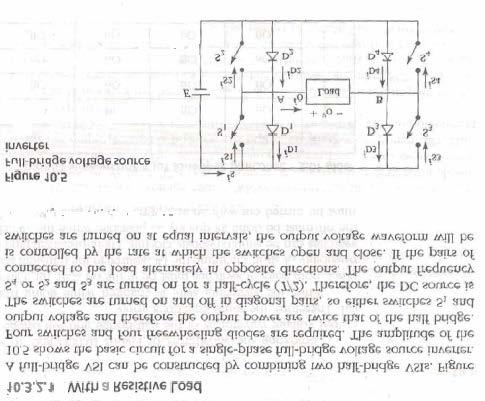
26 IETE 26
27 IETE 27
 =")
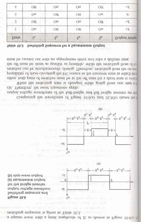
28 b. What are the most commonly used methods of pulse width modulation? Explain multiple pulse width modulation with the help of waveforms when the number of pulses (m) = 2 and 3. (8) Answer: IETE 28
29 IETE 29

30 Q.9 a. What do you mean by AC power control? Discuss the differences between integral cycle control and AC phase control. (8) Answer: IETE 30
31 IETE 31
32 IETE 32
33 IETE 33
34 IETE 34
35 b. Compare the advantages and disadvantages of semiconductor switches over mechanical switches. (8) Answer: IETE 35
36 IETE 36
37 IETE 37
38 IETE 38
39 IETE 39
40 TEXT BOOK I. Power Electronics for Technology, First Impression (2006), Ashfaq Ahmed, Purdue University - Calumet, Pearson Education IETE 40
(a) average output voltage (b) average output current (c) average and rms values of SCR current and (d) input power factor. [16]
![(a) average output voltage (b) average output current (c) average and rms values of SCR current and (d) input power factor. [16]](/thumbs/81/83006678.jpg "(a) average output voltage (b) average output current (c) average and rms values of SCR current and (d) input power factor. [16]") Code No: 07A50204 R07 Set No. 2 1. A single phase fully controlled bridge converter is operated from 230 v, 50 Hz source. The load consists of 10Ω and a large inductance so as to reach the load current
Code No: 07A50204 R07 Set No. 2 1. A single phase fully controlled bridge converter is operated from 230 v, 50 Hz source. The load consists of 10Ω and a large inductance so as to reach the load current
DHANALAKSHMI COLLEGE OF ENGINEERING DEPARTMENT OF ELECTRICAL AND ELECTRONICS ENGINEERING
 DHANALAKSHMI COLLEGE OF ENGINEERING DEPARTMENT OF ELECTRICAL AND ELECTRONICS ENGINEERING Power Diode EE2301 POWER ELECTRONICS UNIT I POWER SEMICONDUCTOR DEVICES PART A 1. What is meant by fast recovery
6. Explain control characteristics of GTO, MCT, SITH with the help of waveforms and circuit diagrams.
 POWER ELECTRONICS QUESTION BANK Unit 1: Introduction 1. Explain the control characteristics of SCR and GTO with circuit diagrams, and waveforms of control signal and output voltage. 2. Explain the different
ELEC4240/ELEC9240 POWER ELECTRONICS
 THE UNIVERSITY OF NEW SOUTH WALES FINAL EXAMINATION JUNE/JULY, 2003 ELEC4240/ELEC9240 POWER ELECTRONICS 1. Time allowed: 3 (three) hours 2. This paper has six questions. Answer any four. 3. All questions
Power Electronics (BEG335EC )
") 1 Power Electronics (BEG335EC ) 2 PURWANCHAL UNIVERSITY V SEMESTER FINAL EXAMINATION - 2003 The figures in margin indicate full marks. Attempt any FIVE questions. Q. [1] [a] A single phase full converter
1 Power Electronics (BEG335EC ) 2 PURWANCHAL UNIVERSITY V SEMESTER FINAL EXAMINATION - 2003 The figures in margin indicate full marks. Attempt any FIVE questions. Q. [1] [a] A single phase full converter
UNIVERSITY QUESTIONS. Unit-1 Introduction to Power Electronics
 UNIVERSITY QUESTIONS Unit-1 Introduction to Power Electronics 1. Give the symbol and characteristic features of the following devices. (i) SCR (ii) GTO (iii) TRIAC (iv) IGBT (v) SIT (June 2012) 2. What
Power Electronics (Sample Questions) Module-1
 Module-1") Module-1 Short Questions (Previous Years BPUT Questions 1 to 18) 1. What are the conditions for a thyristor to conduct? di 2. What is the common method used for protection? dt 3. What is the importance
Module-1 Short Questions (Previous Years BPUT Questions 1 to 18) 1. What are the conditions for a thyristor to conduct? di 2. What is the common method used for protection? dt 3. What is the importance
DC Chopper. Prof. Dr. Fahmy El-khouly
 DC Chopper Prof. Dr. Fahmy El-khouly Definitions: The power electronic circuit which converts directly from dc to dc is called dc-to-dc converter or dc-chopper. Chopper is a dc to dc transformer: The input
R a) Draw and explain VI characteristics of Si & Ge diode. (8M) b) Explain the operation of SCR & its characteristics (8M)
 Draw and explain VI characteristics of Si & Ge diode. (8M) b) Explain the operation of SCR & its characteristics (8M)") SET - 1 1. a) Define i) transient capacitance ii) Diffusion capacitance (4M) b) Explain Fermi level in intrinsic and extrinsic semiconductor (4M) c) Derive the expression for ripple factor of Half wave
SET - 1 1. a) Define i) transient capacitance ii) Diffusion capacitance (4M) b) Explain Fermi level in intrinsic and extrinsic semiconductor (4M) c) Derive the expression for ripple factor of Half wave
11. Define the term pinch off voltage of MOSFET. (May/June 2012)
") Subject Code : EE6503 Branch : EEE Subject Name : Power Electronics Year/Sem. : III /V Unit - I PART-A 1. State the advantages of IGBT over MOSFET. (Nov/Dec 2008) 2. What is the function of snubber circuit?
Subject Code : EE6503 Branch : EEE Subject Name : Power Electronics Year/Sem. : III /V Unit - I PART-A 1. State the advantages of IGBT over MOSFET. (Nov/Dec 2008) 2. What is the function of snubber circuit?
Chapter 6 Soft-Switching dc-dc Converters Outlines
 Chapter 6 Soft-Switching dc-dc Converters Outlines Classification of soft-switching resonant converters Advantages and disadvantages of ZCS and ZVS Zero-current switching topologies The resonant switch
ELEC387 Power electronics
 ELEC387 Power electronics Jonathan Goldwasser 1 Power electronics systems pp.3 15 Main task: process and control flow of electric energy by supplying voltage and current in a form that is optimally suited
EE POWER ELECTRONICS
 EE6503 - POWER ELECTRONICS UNIT III - DC TO DC CONVERTER PART A 1.What is meant by time ratio or PWM control (duty cycle) of a DC chopper? (M/J16) The ratio of a period to the total time period is known
INSTITUTE OF AERONAUTICAL ENGINEERING (Autonomous) Dundigal, Hyderabad
 Dundigal, Hyderabad") I INSTITUTE OF AERONAUTICAL ENGINEERING (Autonomous) Dundigal, Hyderabad-000 DEPARTMENT OF ELECTRICAL AND ELECTRONICS ENGINEERING TUTORIAL QUESTION BANK Course Name : POWER ELECTRONICS Course Code : AEE0
I INSTITUTE OF AERONAUTICAL ENGINEERING (Autonomous) Dundigal, Hyderabad-000 DEPARTMENT OF ELECTRICAL AND ELECTRONICS ENGINEERING TUTORIAL QUESTION BANK Course Name : POWER ELECTRONICS Course Code : AEE0
ELG3336: Power Electronics Systems Objective To Realize and Design Various Power Supplies and Motor Drives!
 ELG3336: Power Electronics Systems Objective To Realize and Design arious Power Supplies and Motor Drives! Power electronics refers to control and conversion of electrical power by power semiconductor
VALLIAMMAI ENGINEERING COLLEGE DEPARTMENT OF ELECTRONICS AND INSTRUMENTATION
 VALLIAMMAI ENGINEERING COLLEGE DEPARTMENT OF ELECTRONICS AND INSTRUMENTATION Sem / Branch : V /EIE Subject code /Title: EI2301/Industrial Electronics UNIT-1 POWER DEVICES 1. What are the different methods
Appendix: Power Loss Calculation
 Appendix: Power Loss Calculation Current flow paths in a synchronous buck converter during on and off phases are illustrated in Fig. 1. It has to be noticed that following parameters are interrelated:
AC Theory and Electronics
 AC Theory and Electronics An Alternating Current (AC) or Voltage is one whose amplitude is not constant, but varies with time about some mean position (value). Some examples of AC variation are shown below:
DHANALAKSHMI SRINIVASAN COLLEGE OF ENGINEERING AND TECHNOLY Mamallapuram chennai
 DHANALAKSHMI SRINIVASAN COLLEGE OF ENGINEERING AND TECHNOLY Mamallapuram chennai DEPARTMENT OF ELECTRICAL AND ELECTRONICS ENGINEERING QUESTION BANK V SEMESTER EE6503 - POWER ELECTRONICS Regulation 2013
Subject Code: Model Answer Page No: / N
 Important Instructions to examiners: 1) The answers should be examined by key words and not as word-to-word as given in the model answer scheme. 2) The model answer and the answer written by candidate
The typical ratio of latching current to holding current in a 20 A thyristor is (A) 5.0 (B) 2.0 (C) 1.0 (D) 0.5
 5.0 (B) 2.0 (C) 1.0 (D) 0.5") CHAPTER 9 POWER ELECTRONICS YEAR 0 ONE MARK MCQ 9. MCQ 9. A half-controlled single-phase bridge rectifier is supplying an R-L load. It is operated at a firing angle α and the load current is continuous.
CHAPTER 9 POWER ELECTRONICS YEAR 0 ONE MARK MCQ 9. MCQ 9. A half-controlled single-phase bridge rectifier is supplying an R-L load. It is operated at a firing angle α and the load current is continuous.
Obsolete Product(s) - Obsolete Product(s)
 - Obsolete Product(s)") DMOS DUAL FULL BRIDGE DRIVER SUPPLY VOLTAGE UP TO 48V R DS(ON) 1.2Ω L6204 (25 C) CROSS CONDUCTION PROTECTION THERMAL SHUTDOWN 0.5A DC CURRENT TTL/CMOS COMPATIBLE DRIVER HIGH EFFICIENCY CHOPPING MULTIPOWER
DMOS DUAL FULL BRIDGE DRIVER SUPPLY VOLTAGE UP TO 48V R DS(ON) 1.2Ω L6204 (25 C) CROSS CONDUCTION PROTECTION THERMAL SHUTDOWN 0.5A DC CURRENT TTL/CMOS COMPATIBLE DRIVER HIGH EFFICIENCY CHOPPING MULTIPOWER
Dr.Arkan A.Hussein Power Electronics Fourth Class. Commutation of Thyristor-Based Circuits Part-I
 Commutation of Thyristor-Based Circuits Part-I ١ This lesson provides the reader the following: (i) (ii) (iii) (iv) Requirements to be satisfied for the successful turn-off of a SCR The turn-off groups
Sample Exam Solution
 Session 44; 1/6 Sample Exam Solution Problem 1: You are given a single phase diode rectifier, as shown below. Do the following: L d I s v (t) s L s C d V d Load : 310V Xs : 0.4ohm at 400 Hz Vspk : 360V
ECEN4797/5797 Lecture #11
 ECEN4797/5797 Lecture #11 Announcements On-campus students: pick up graded HW2, turn in HW3 Homework 4 is due in class on Friday, Sept. 23. The grace-period for offcampus students expires 5pm (Mountain)
R. W. Erickson. Department of Electrical, Computer, and Energy Engineering University of Colorado, Boulder
 R. W. Erickson Department of Electrical, Computer, and Energy Engineering University of Colorado, Boulder Inclusion of Switching Loss in the Averaged Equivalent Circuit Model The methods of Chapter 3 can
Operating Junction and 55 to +175 C Storage Temperature Range
 Feathers: dvanced trench process technology avalanche energy, 100% test Fully characterized avalanche voltage and current ID =60 BV=60V Rdson=14mΩ(max.) Description: The is a new generation of middle voltage
SIMULATION STUDIES OF HALF-BRIDGE ISOLATED DC/DC BOOST CONVERTER
 POZNAN UNIVE RSITY OF TE CHNOLOGY ACADE MIC JOURNALS No 80 Electrical Engineering 2014 Adam KRUPA* SIMULATION STUDIES OF HALF-BRIDGE ISOLATED DC/DC BOOST CONVERTER In order to utilize energy from low voltage
High Voltage DC Transmission 2
 High Voltage DC Transmission 2 1.0 Introduction Interconnecting HVDC within an AC system requires conversion from AC to DC and inversion from DC to AC. We refer to the circuits which provide conversion
( ) ON s inductance of 10 mh. The motor draws an average current of 20A at a constant back emf of 80 V, under steady state.
 ON s inductance of 10 mh. The motor draws an average current of 20A at a constant back emf of 80 V, under steady state.") 1991 1.12 The operating state that distinguishes a silicon controlled rectifier (SCR) from a diode is (a) forward conduction state (b) forward blocking state (c) reverse conduction state (d) reverse blocking
1991 1.12 The operating state that distinguishes a silicon controlled rectifier (SCR) from a diode is (a) forward conduction state (b) forward blocking state (c) reverse conduction state (d) reverse blocking
Design of a Cell Charger for an ipad Using Full Bridge Rectifier and Flyback Converter
 Design of a Cell Charger for an ipad Using Full Bridge Rectifier and Flyback Converter 1 Ali Saleh Aziz, 2 Riyadh Nazar Ali 1, 2 Assistant Lecturer 1, 2 Department of Medical Instruments Techniques Engineering
UNIT-III STATOR SIDE CONTROLLED INDUCTION MOTOR DRIVE
 UNIT-III STATOR SIDE CONTROLLED INDUCTION MOTOR DRIVE 3.1 STATOR VOLTAGE CONTROL The induction motor 'speed can be controlled by varying the stator voltage. This method of speed control is known as stator
MICROCONTROLLER BASED BOOST PID MUNAJAH BINTI MOHD RUBAEE
 MICROCONTROLLER BASED BOOST PID MUNAJAH BINTI MOHD RUBAEE This thesis is submitted as partial fulfillment of the requirement for the award of Bachelor of Electrical Engineering (Power System) Faculty of
POWER ELECTRONICS PO POST GRAD POS UATE 2010 AC Ch AC o Ch p o per Prepare Prep d are by: d Dr. Gamal Gam SOwilam SOwila 11 December 2016 ١
 POWER ELECTRONICS POST GRADUATE 2010 AC Chopper Prepared by: Dr. Gamal SOwilam 11 December 2016 ١ 1. Introduction AC Chopper is An AC to AC Converter employs to vary the rms voltage across the load at
POWER ELECTRONICS. Alpha. Science International Ltd. S.C. Tripathy. Oxford, U.K.
 POWER ELECTRONICS S.C. Tripathy Alpha Science International Ltd. Oxford, U.K. Contents Preface vii 1. SEMICONDUCTOR DIODE THEORY 1.1 1.1 Introduction 1.1 1.2 Charge Densities in a Doped Semiconductor 1.1
POWER ELECTRONICS LAB
 MUFFAKHAM JAH COLLEGE OF ENGINEERING & TECHNOLOGY Banjara Hills Road No 3, Hyderabad 34 www.mjcollege.ac.in DEPARTMENT OF ELECTRICAL ENGINEERING LABORATORY MANUAL POWER ELECTRONICS LAB For B.E. III/IV
Class D Audio Amplifier Design
 Class D Audio Amplifier Design Class D Amplifier Introduction Theory of Class D operation, topology comparison Gate Driver How to drive the gate, key parameters in gate drive stage MOSFET How to choose,
Power Electronics. Contents
 Power Electronics Overview Contents Electronic Devices Power, Electric, Magnetic circuits Rectifiers (1-ph, 3-ph) Converters, controlled rectifiers Inverters (1-ph, 3-ph) Power system harmonics Choppers
WPT2N32 WPT2N32. Descriptions. Features. Applications. Order information. Http//:
 Single, PNP, -30V, -A, Power Transistor with 20V N-MOSFET Http//:www.willsemi.com Descriptions The is PNP bipolar power transistor with 20V N-MOSFET. This device is suitable for use in charging circuit
DHANALAKSHMI COLLEGE OF ENGINEERING DEPARTMENT OF ELECTRICAL AND ELECTRONICS ENGINEERING EC6202 ELECTRONIC DEVICES AND CIRCUITS
 DHANALAKSHMI COLLEGE OF ENGINEERING DEPARTMENT OF ELECTRICAL AND ELECTRONICS ENGINEERING EC6202 ELECTRONIC DEVICES AND CIRCUITS UNIT-I - PN DIODEAND ITSAPPLICATIONS 1. What is depletion region in PN junction?
POWER ELECTRONICS LAB MANUAL
 JIS College of Engineering (An Autonomous Institution) Department of Electrical Engineering POWER ELECTRONICS LAB MANUAL Exp-1. Study of characteristics of an SCR AIM: To obtain the V-I characteristics
EXPERIMENT 4 SWITCHED MODE DC/DC CONVERSION USING BUCK CONVERTER
 Introduction: YEDITEPE UNIERSITY ENGINEERING & ARHITETURE FAULTY INDUSTRIAL ELETRONIS LABORATORY EE 432 INDUSTRIAL ELETRONIS EXPERIMENT 4 SWITHED MODE D/D ONERSION USING BUK ONERTER In this experiment,
EEL 5245 POWER ELECTRONICS I Lecture #4: Chapter 2 Switching Concepts and Semiconductor Overview
 EEL 5245 POWER ELECTRONICS I Lecture #4: Chapter 2 Switching Concepts and Semiconductor Overview Objectives of Lecture Switch realizations Objective is to focus on terminal characteristics Blocking capability
18 N Amps, 500 Volts N-CHANNEL MOSFET. Power MOSFET DESCRIPTION FEATURES SYMBOL
 Power MOSFET 8 Amps, 500 Volts NCHANNEL MOSFET DESCRIPTION The YR 8N50 are NChannel enhancement mode power field effect transistors (MOSFET) which are produced using YR s proprietary,planar stripe, DMOS
Experiment DC-DC converter
 POWER ELECTRONIC LAB Experiment-7-8-9 DC-DC converter Power Electronics Lab Ali Shafique, Ijhar Khan, Dr. Syed Abdul Rahman Kashif 10/11/2015 This manual needs to be completed before the mid-term examination.
IRF130, IRF131, IRF132, IRF133
 October 1997 SEMICONDUCTOR IRF13, IRF131, IRF132, IRF133 12A and 14A, 8V and 1V,.16 and.23 Ohm, N-Channel Power MOSFETs Features Description 12A and 14A, 8V and 1V r DS(ON) =.16Ω and.23ω Single Pulse Avalanche
University of Washington Department of Electrical Engineering EE 351: Introduction to Energy Devices and Systems. Lab 1: Power Electronic Converters
 University of Washington Department of Electrical Engineering EE 351: Introduction to Energy Devices and Systems Lab 1: Power Electronic Converters Introduction With the development of power electronic
R. W. Erickson. Department of Electrical, Computer, and Energy Engineering University of Colorado, Boulder
 R. W. Erickson Department of Electrical, Computer, and Energy Engineering University of Colorado, Boulder pn junction! Junction diode consisting of! p-doped silicon! n-doped silicon! A p-n junction where
International Journal of Advance Engineering and Research Development
 Scientific Journal of Impact Factor (SJIF): 4.72 International Journal of Advance Engineering and Research Development Volume 4, Issue 8, August -2017 e-issn (O): 2348-4470 p-issn (P): 2348-6406 Analysis
N & P-Channel 100-V (D-S) MOSFET
 MOSFET") N & P-Channel -V (D-S) MOSFET Key Features: Low r DS(on) trench technology Low thermal impedance Fast switching speed Typical Applications: LED Inverter Circuits DC/DC Conversion Circuits Motor drives
N & P-Channel -V (D-S) MOSFET Key Features: Low r DS(on) trench technology Low thermal impedance Fast switching speed Typical Applications: LED Inverter Circuits DC/DC Conversion Circuits Motor drives
TSP13N 50M / TSF13N N50M
 TSP13N50M / TSF13N50M 600V N-Channel MOSFET General Description This Power MOSFET is produced using True semi s advanced planar stripe DMOS technology. This advanced technology has been especially tailored
Super Junction MOSFET
 65V 94A * *G Denotes RoHS Compliant, Pb Free Terminal Finish. CO LMOS Power Semiconductors Super Junction MOSFET T-Max TM Ultra Low R DS(ON) Low Miller Capacitance Ultra Low Gate Charge, Q g Avalanche
Module 3. DC to DC Converters. Version 2 EE IIT, Kharagpur 1
 Module 3 DC to DC Converters Version 2 EE IIT, Kharagpur 1 Lesson 2 Commutation of Thyristor-Based Circuits Part-II Version 2 EE IIT, Kharagpur 2 This lesson provides the reader the following: (i) (ii)
List of Experiments. 1. Steady state characteristics of SCR, IGBT and MOSFET. (Single phase half wave rectifier). (Simulation and hardware).
. (Simulation and hardware).") (Scheme-2013) List of Experiments 1. Steady state characteristics of SCR, IGBT and MOSFET 2. nalog and digital firing methods for SCR (Single phase half wave rectifier). (Simulation and hardware). 3. Full
(Scheme-2013) List of Experiments 1. Steady state characteristics of SCR, IGBT and MOSFET 2. nalog and digital firing methods for SCR (Single phase half wave rectifier). (Simulation and hardware). 3. Full
ELG4139: Power Electronics Systems Objective To Realize and Design Various Power Supplies and Motor Drives!
 ELG4139: Power Electronics Systems Objective To Realize and Design Various Power Supplies and Motor Drives! Power electronics refers to control and conversion of electrical power by power semiconductor
EE204 Basic Electronics and Electric Power Course Notes Energy Sources and Power Conversion
 Energy Sources and Power Conversion This Section will discuss some of the ways energy is provided to electronic and electromechanical devices In most cases, the voltages required for various purposes are
Fundamentals of Power Electronics
 Fundamentals of Power Electronics SECOND EDITION Robert W. Erickson Dragan Maksimovic University of Colorado Boulder, Colorado Preface 1 Introduction 1 1.1 Introduction to Power Processing 1 1.2 Several
FREQUENTLY ASKED QUESTIONS
 FREQUENTLY ASKED QUESTIONS UNIT-1 SUBJECT : ELECTRONIC DEVICES AND CIRCUITS SUBJECT CODE : EC6202 BRANCH: EEE PART -A 1. What is meant by diffusion current in a semi conductor? (APR/MAY 2010, 2011, NOV/DEC
Super Junction MOSFET
 APT77N6BC6 APT77N6SC6 6V 77A.4Ω CO LMOS Power Semiconductors Super Junction MOSFET Ultra Low R DS(ON) TO-247 Low Miller Capacitance D 3 PAK Ultra Low Gate Charge, Q g Avalanche Energy Rated Extreme dv
Other Electronic Devices
 Other Electronic Devices 1 Contents Field-Effect Transistors(FETs) - JFETs - MOSFETs Insulate Gate Bipolar Transistors(IGBTs) H-bridge driver and PWM Silicon-Controlled Rectifiers(SCRs) TRIACs Device Selection
IRGBC30M Short Circuit Rated Fast IGBT
 INSULTED GTE BIPOLR TRNSISTOR Features Short circuit rated - µs @ 25, V GE = 5V Switching-loss rating includes all "tail" losses Optimized for medium operating frequency ( to khz) See Fig. for urrent vs.
HCI70R500E 700V N-Channel Super Junction MOSFET
 HCI70R500E 700V N-Channel Super Junction MOSFET Features Very Low FOM (R DS(on) X Q g ) Extremely low switching loss Excellent stability and uniformity 100% Avalanche Tested Higher dv/dt ruggedness Application
Module 1. Power Semiconductor Devices. Version 2 EE IIT, Kharagpur 1
 Module 1 Power Semiconductor Devices Version EE IIT, Kharagpur 1 Lesson 8 Hard and Soft Switching of Power Semiconductors Version EE IIT, Kharagpur This lesson provides the reader the following (i) (ii)
R. W. Erickson. Department of Electrical, Computer, and Energy Engineering University of Colorado, Boulder
 R. W. Erickson Department of Electrical, Computer, and Energy Engineering University of Colorado, Boulder 18.5 RMS values of rectifier waveforms Doubly-modulated transistor current waveform, boost rectifier:
Name of chapter & details
 Course Title Course Code Power Electronics-I EL509 Lecture : 03 / 03 Course Credit / Hours Practical : 01 / 02 Tutorial : 00 / 00 Course Learning Outcomes Total : 04 / 05 At the end of the session student
Chapter 1 INTRODUCTION TO POWER ELECTRONICS SYSTEMS
 Chapter 1 INTRODUCTION TO POWER ELECTRONICS SYSTEMS Definition and concepts Application Power semiconductor switches Gate/base drivers Losses Snubbers 1 Definition of Power Electronics DEFINITION: To convert,
SINGLE-STAGE HIGH-POWER-FACTOR SELF-OSCILLATING ELECTRONIC BALLAST FOR FLUORESCENT LAMPS WITH SOFT START
 SINGLE-STAGE HIGH-POWER-FACTOR SELF-OSCILLATING ELECTRONIC BALLAST FOR FLUORESCENT S WITH SOFT START Abstract: In this paper a new solution to implement and control a single-stage electronic ballast based
AO4912 Asymmetric Dual N-Channel Enhancement Mode Field Effect Transistor
 Asymmetric Dual N-Channel Enhancement Mode Field Effect Transistor General Description The AO49 uses advanced trench technology to provide excellent R DS(ON) and low gate charge. The two MOSFETs make a
Improvements of LLC Resonant Converter
 Chapter 5 Improvements of LLC Resonant Converter From previous chapter, the characteristic and design of LLC resonant converter were discussed. In this chapter, two improvements for LLC resonant converter
International Journal of Scientific & Engineering Research, Volume 5, Issue 3, March-2014 ISSN
 332 An Improved Bridgeless SEPIC PFC Converter N. Madhumitha, Dr C. Christober Asir Rajan Department of Electrical & Electronics Engineering Pondicherry Engineering College madhudeez@pec.edu, asir_70@pec.edu
13. DC to AC Converters
 13. DC to AC Converters Inverters Inverter is a device which converts DC voltages (or current) to AC voltages (or current).inverter converting voltage is called VOLTAGE SOURCE INVERTER (VSI), while inverter
HCD80R600R 800V N-Channel Super Junction MOSFET
 HCD80R600R 800V N-Channel Super Junction MOSFET Features Very Low FOM (R DS(on) X Q g ) Extremely low switching loss Excellent stability and uniformity 00% Avalanche Tested Application Switch Mode Power
Development of a Single-Phase PWM AC Controller
 Pertanika J. Sci. & Technol. 16 (2): 119-127 (2008) ISSN: 0128-7680 Universiti Putra Malaysia Press Development of a Single-Phase PWM AC Controller S.M. Bashi*, N.F. Mailah and W.B. Cheng Department of
Single-Phase Full-Wave Phase-Controlled Rectifier
 + 2004.10.09 EE410L, Experiment #1 Brett Allan I. Introduction The objective of this experiment is to design, construct, and test a Single-Phase Full-Wave Phase-Controlled Rectifier. The subsequent block
 Code No: Y0221/R07 Set No. 1 I B.Tech Supplementary Examinations, Apr/May 2013 BASIC ELECTRONIC DEVICES AND CIRCUITS (Electrical & Electronics Engineering) Time: 3 hours Max Marks: 80 Answer any FIVE Questions
Features. Symbol JEDEC TO-204AA GATE (PIN 1)
") Semiconductor BUZB Data Sheet October 998 File Number 9. [ /Title (BUZ B) /Subject A, V,. hm, N- hannel ower OS- ET) /Author ) /Keyords Harris emionducor, N- hannel ower OS- ET, O- AA) /Creator ) /DOCIN
Semiconductor BUZB Data Sheet October 998 File Number 9. [ /Title (BUZ B) /Subject A, V,. hm, N- hannel ower OS- ET) /Author ) /Keyords Harris emionducor, N- hannel ower OS- ET, O- AA) /Creator ) /DOCIN
Lecture 19 - Single-phase square-wave inverter
 Lecture 19 - Single-phase square-wave inverter 1. Introduction Inverter circuits supply AC voltage or current to a load from a DC supply. A DC source, often obtained from an AC-DC rectifier, is converted
Features. Symbol Parameter Rating Units V DS Drain-Source Voltage 60 V V GS Gate-Source Voltage ±20 V
 General Description These N-Channel enhancement mode power field effect transistors are using trench DMOS technology. This advanced technology has been especially tailored to minimize on-state resistance,
Lecture 41 SIMPLE AVERAGING OVER T SW to ACHIEVE LOW FREQUENCY MODELS
 Lecture 41 SIMPLE AVERAGING OVER T SW to ACHIEVE LOW FREQUENCY MODELS. Goals and Methodology to Get There 0. Goals 0. Methodology. BuckBoost and Other Converter Models 0. Overview of Methodology 0. Example
AN2170 APPLICATION NOTE MOSFET Device Effects on Phase Node Ringing in VRM Power Converters INTRODUCTION
 AN2170 APPLICATION NOTE MOSFET Device Effects on Phase Node Ringing in VRM Power Converters INTRODUCTION The growth in production volume of industrial equipment (e.g., power DC-DC converters devoted to
Features. Symbol Parameter Rating Units V DS Drain-Source Voltage 650 V V GS Gate-Source Voltage ±30 V
 General Description These N-Channel enhancement mode power field effect transistors are using Super Junction technology. This advanced technology has been especially tailored to minimize on-state resistance,
DEVELOPMENT OF A GATE DRIVE WITH OVERCURRENT PROTECTION CIRCUIT USING IR2110 FOR FAST SWITCHING HALF- BRIDGE CONVERTER
 DEVELOPMENT OF A GATE DRIVE WITH OVERCURRENT PROTECTION CIRCUIT USING IR2110 FOR FAST SWITCHING HALF- BRIDGE CONVERTER R. Baharom, K. S. Muhammad, M. N. Seroji and M. K. M. Salleh Faculty of Electrical
SGP100N09T. Symbol Parameter SGP100N09T Unit. 70* -Continuous (TA = 100 )
") SUPER-SEMI SUPER-MOSFET Super Gate Metal Oxide Semiconductor Field Effect Transistor 100V Super Gate Power Transistor SG*100N09T Rev. 1.01 Jun. 2016 SGP100N09T 100V N-Channel MOSFET Description The SG-MOSFET
SUPER-SEMI SUPER-MOSFET Super Gate Metal Oxide Semiconductor Field Effect Transistor 100V Super Gate Power Transistor SG*100N09T Rev. 1.01 Jun. 2016 SGP100N09T 100V N-Channel MOSFET Description The SG-MOSFET
AOL1422 N-Channel Enhancement Mode Field Effect Transistor
 N-Channel Enhancement Mode Field Effect Transistor General Description The uses advanced trench technology and design to provide excellent R DS(ON) with low gate charge. This device is ESD protected and
EEL 646 POWER ELECTRONICS II. Issa Batarseh. January 13, 2015
 EEL 646 POWER ELECTRONICS II Issa Batarseh January 13, 2015 Agenda About the course Syllabus Review Course Topics Review of Power Electronics I Questions Introduction (cont d) Introduction (cont d) 5
CHAPTER 2 DESIGN AND MODELING OF POSITIVE BUCK BOOST CONVERTER WITH CASCADED BUCK BOOST CONVERTER
 17 CHAPTER 2 DESIGN AND MODELING OF POSITIVE BUCK BOOST CONVERTER WITH CASCADED BUCK BOOST CONVERTER 2.1 GENERAL Designing an efficient DC to DC buck-boost converter is very much important for many real-time
Questions from the same exercise can be combined together to increase difficulty. Which one of the following properties of the diode is NOT true:
 Questions from the same exercise can be combined together to increase difficulty. 21 1 Which one of the following properties of the diode is NOT true: a) When no voltage is applied across the diode, it
L MOSFETS, IDENTIFICATION, CURVES. PAGE 1. I. Review of JFET (DRAW symbol for n-channel type, with grounded source)
") L.107.4 MOSFETS, IDENTIFICATION, CURVES. PAGE 1 I. Review of JFET (DRAW symbol for n-channel type, with grounded source) 1. "normally on" device A. current from source to drain when V G = 0 no need to
L.107.4 MOSFETS, IDENTIFICATION, CURVES. PAGE 1 I. Review of JFET (DRAW symbol for n-channel type, with grounded source) 1. "normally on" device A. current from source to drain when V G = 0 no need to
INVESTIGATION OF GATE DRIVERS FOR SNUBBERLESS OVERVOLTAGE SUPPRESSION OF POWER IGBTS
 INVESTIGATION OF GATE DRIVERS FOR SNUBBERLESS OVERVOLTAGE SUPPRESSION OF POWER IGBTS Alvis Sokolovs, Iļja Galkins Riga Technical University, Department of Power and Electrical Engineering Kronvalda blvd.
235 W Maximum Power Dissipation (whole module) 470 T J Junction Operating Temperature -40 to 150. Torque strength
 470 T J Junction Operating Temperature -40 to 150. Torque strength") Discontinued PRODUCT SUMMARY (TYPICAL) V DS (V) 600 R DS(on) (m ) 30 GaN Power Hybrid HEMT Half-Bridge Module Features High frequency operation Free-wheeling diode not required Applications Compact DC-DC
Discontinued PRODUCT SUMMARY (TYPICAL) V DS (V) 600 R DS(on) (m ) 30 GaN Power Hybrid HEMT Half-Bridge Module Features High frequency operation Free-wheeling diode not required Applications Compact DC-DC
Features. Symbol Parameter Rating Units V DS Drain-Source Voltage 20 V V GS Gate-Source Voltage ±10 V
 General Description These N-Channel enhancement mode power field effect transistors are using trench DMOS technology. This advanced technology has been especially tailored to minimize on-state resistance,
Code No: R Set No. 1
 Code No: R05010204 Set No. 1 I B.Tech Supplimentary Examinations, Aug/Sep 2007 ELECTRONIC DEVICES AND CIRCUITS ( Common to Electrical & Electronic Engineering, Electronics & Communication Engineering,
POWER ELECTRONICS. Converters, Applications, and Design. NED MOHAN Department of Electrical Engineering University of Minnesota Minneapolis, Minnesota
 POWER ELECTRONICS Converters, Applications, and Design THIRD EDITION NED MOHAN Department of Electrical Engineering University of Minnesota Minneapolis, Minnesota TORE M. UNDELAND Department of Electrical
Field-Effect Transistor (FET) is one of the two major transistors; FET derives its name from its working mechanism;
 is one of the two major transistors; FET derives its name from its working mechanism;") Chapter 3 Field-Effect Transistors (FETs) 3.1 Introduction Field-Effect Transistor (FET) is one of the two major transistors; FET derives its name from its working mechanism; The concept has been known
Chapter 3 Field-Effect Transistors (FETs) 3.1 Introduction Field-Effect Transistor (FET) is one of the two major transistors; FET derives its name from its working mechanism; The concept has been known
ZCS-PWM Converter for Reducing Switching Losses
 IOSR Journal of Electrical and Electronics Engineering (IOSR-JEEE) e-issn: 2278-1676,p-ISSN: 2320-3331, Volume 9, Issue 1 Ver. III (Jan. 2014), PP 29-35 ZCS-PWM Converter for Reducing Switching Losses
MDF10N60G N-Channel MOSFET 600V, 10A, 0.7Ω
 MDFNG N-channel MOSFET V MDFNG N-Channel MOSFET V, A,.7Ω General Description These N-channel MOSFET are produced using advanced MagnaChip s MOSFET Technology, which provides low onstate resistance, high
S2 6 1 S1 3 D2 2 G1. Pin configuration (Top view) Parameter Symbol 10 S Steady State Unit Drain-Source Voltage V DS +20 Gate-Source Voltage V GS 6
 Parameter Symbol 10 S Steady State Unit Drain-Source Voltage V DS +20 Gate-Source Voltage V GS 6") Descriptions Features and Applications The SOT-363 is N-Channel enhancement MOS Field Effect Transistor. Uses advanced trench technology and design to provide excellent R DS (ON) with low gate charge.
Descriptions Features and Applications The SOT-363 is N-Channel enhancement MOS Field Effect Transistor. Uses advanced trench technology and design to provide excellent R DS (ON) with low gate charge.
LINEAR IC APPLICATIONS
 1 B.Tech III Year I Semester (R09) Regular & Supplementary Examinations December/January 2013/14 1 (a) Why is R e in an emitter-coupled differential amplifier replaced by a constant current source? (b)
A Highly Versatile Laboratory Setup for Teaching Basics of Power Electronics in Industry Related Form
 A Highly Versatile Laboratory Setup for Teaching Basics of Power Electronics in Industry Related Form JOHANN MINIBÖCK power electronics consultant Purgstall 5 A-3752 Walkenstein AUSTRIA Phone: +43-2913-411
Scheme I Sample. : Second : Basic. Electronics : 70. Marks. Time: 3 Hrs. 2] b) State any. e) State any. Figure Definition.
![Scheme I Sample. : Second : Basic. Electronics : 70. Marks. Time: 3 Hrs. 2] b) State any. e) State any. Figure Definition.](/thumbs/96/128002629.jpg "Scheme I Sample. : Second : Basic. Electronics : 70. Marks. Time: 3 Hrs. 2] b) State any. e) State any. Figure Definition.") Program Name Program Code Semester Course Title Scheme I Sample Question Paper : Diploma in Electronics Program Group : DE/EJ/IE/IS/ET/EN/EX : Second : Basic Electronics : 70 22216 Time: 3 Hrs. Instructions:
Program Name Program Code Semester Course Title Scheme I Sample Question Paper : Diploma in Electronics Program Group : DE/EJ/IE/IS/ET/EN/EX : Second : Basic Electronics : 70 22216 Time: 3 Hrs. Instructions: