XC6201 Series GENERAL DESCRIPTION FEATURES APPLICATIONS TYPICAL PERFORMANCE CHARACTERISTICS TYPICAL APPLICATION CIRCUIT. Positive Voltage Regulators
|
|
|
- Amber Phillips
- 5 years ago
- Views:
Transcription

1 ETR0301_004 Positive Voltage Regulators GENERAL DESCRIPTION The XC6201 series are highly precise, low power consumption, positive voltage regulators manufactured using CMOS and laser trimming technologies. The series provides large currents with a significantly small dropout voltage. The XC6201 consists of a current limiter circuit, a driver transistor, a precision reference voltage and an error amplifier. Output voltage is selectable in 0.1V steps between 1.3V ~ 6.0V. SOT-25, SOT-89, USP-6B and TO-92 packages are available. APPLICATIONS Mobile Phones Cordless phones, wireless communication equipment Cameras, video recorders Portable games Portable AV equipment Reference voltage Battery powered equipment FEATURES Maximum Output Current : 250mA (TYP.) Dropout Voltage : 100mA : 200mA Maximum Operating Voltage : 10V Output Voltage Range : 1.3V ~ 6.0V (0.1V increments) Fixed Voltage Accuracy : ±1% (V OUT(T) >2.0V) ±2% Low Power Consumption : 2.0μA (TYP.) Operational Temperature Range : -40 ~ 85 Packages : SOT-25, SOT-89 TO-92 USP-6B Environmentally Friendly : EU RoHS Compliant, Pb Free Tantalum or Ceramic Capacitor compatible TYPICAL APPLICATION CIRCUIT TYPICAL PERFORMANCE CHARACTERISTICS Supply Current vs. Input Voltage XC6201P332 1/24
2 PIN CONFIGURATION NC VSS NC VIN NC VOUT PIN ASSIGNMENT (SIDE VIEW) *The dissipation pad for the USP-6B package should be solder-plated in recommended mount pattern and metal masking so as to enhance mounting strength and heat release. If the pad needs to be connected to other pins, it should be connected to the VSS (No.5) pin. PIN NUMBER SOT-25 SOT-89/TO-92 (T) USP-6B PIN NAME FUNCTION VOUT Output VSS Ground VIN Power Input 3, 4-2,4,6 NC No Connection PRODUCT CLASSIFICATION Ordering Information X C P (*1) 1 2 DESIGNATOR DESCRIPTION SYMBOL DESCRIPTION 1 Product Number 01-2 Type of Regulator P 3-pin regulator e.g. 30:3.0V 34 Output Voltage 13~60 50:5.0V 1 ±1% 5 Output Voltage Accuracy 2 ±2% 67-8 Packages Taping Type (*2) MR MR-G PR PR-G TH TH-G TB TB-G DR DR-G SOT-25 SOT-25 SOT-89 SOT-89 TO-92 Taping Type: Paper type TO-92 Taping Type: Paper type TO-92 Taping Type: Bag TO-92 Taping Type: Bag USP-6B USP-6B * +1% accuracy can be set at V OUT(T) > 2.0V. (*1) (*2) The -G suffix indicates that the products are Halogen and Antimony free as well as being fully RoHS compliant. The device orientation is fixed in its embossed tape pocket. For reverse orientation, please contact your local Torex sales office or representative. (Standard orientation: 6R-8, Reverse orientation: 6L-8) 2/24
3 XC6201 Series BLOCK DIAGRAM ABSOLUTE MAXIMUM RATINGS Ta = 25 PARAMETER SYMBOL RATINGS UNITS Input Voltage VIN 12.0 V Output Current IOUT 500 ma Output Voltage VOUT VSS-0.3~VIN+0.3 V SOT Power SOT Pd Dissipation TO mw USP-6B 120 Operating Temperature Range Topr -40~+85 Storage Temperature Range Tstg -55~+125 ELECTRICAL CHARACTERISTICS XC6201P132 VOUT(T)=1.3V ( *1) PARAMETER SYMBOL CONDITIONS MIN. TYP. MAX. UNITS CIRCUIT Output Voltage VOUT(E) ( *2) VIN=2.3V IOUT=10mA V 2 Maximum Output Current IOUTmax VIN=2.3V VOUT(E) 1.17V ma 2 Load Regulation VIN=2.3V 1mA IOUT 30mA mv 2 Dropout Voltage ( *3) Vdif1 IOUT=30mA Vdif2 IOUT=60mA mv 2 Supply Current ISS VIN=2.3V μa 1 Line Regulation IOUT=10mA VIN 2.3V VIN 10.0V %/V 2 Input Voltage VIN V - Output Voltage Temperature Characteristics Topr -40 Topr 85 Ta=25 - ±100 - ppm/ 2 3/24
4 ELECTRICAL CHARACTERISTICS (Continued) XC6201P182 VOUT(T)=1.8V ( *1) Ta=25 PARAMETER SYMBOL CONDITIONS MIN. TYP. MAX. UNITS CIRCUIT Output Voltage VOUT(E) ( *2) VIN=2.8V V 2 Maximum Output Current IOUTmax VIN=2.8V VOUT(E) 1.62V ma 2 Load Regulation VIN=2.8V 1mA IOUT 40mA mv 2 Dropout Voltage ( *3) Vdif Vdif2 IOUT=80mA mv 2 Supply Current ISS VIN=2.8V μa 1 Line Regulation VIN 2.8V VIN 10.0V %/V 2 Input Voltage VIN V - Output Voltage Temperature Characteristics Topr -40 Topr 85 - ±100 - ppm/ 2 XC6201P272 VOUT(T)=2.7V ( *1) PARAMETER SYMBOL CONDITIONS MIN. TYP. MAX. UNITS CIRCUIT Output Voltage VOUT(E) ( *2) VIN=3.7V V 2 Maximum Output Current IOUTmax VIN=3.7V VOUT(E) 2.43V ma 2 Load Regulation VIN=3.7V 1mA IOUT 60mA mv 2 Dropout Voltage ( *3) Vdif1 IOUT=60mA Vdif2 IOUT=120mA mv 2 Supply Current ISS VIN=3.7V μa 1 Line Regulation VIN 3.7V VIN 10.0V %/V 2 Input Voltage VIN V - Output Voltage Temperature Characteristics Topr -40 Topr 85 Ta=25 - ±100 - ppm/ 2 4/24
5 XC6201 Series ELECTRICAL CHARACTERISTICS (Continued) XC6201P332 VOUT(T)=3.3V ( *1) Ta=25 PARAMETER SYMBOL CONDITIONS MIN. TYP. MAX. UNITS CIRCUIT Output Voltage VOUT(E) ( *2) VIN=4.3V V 2 Maximum Output Current IOUTmax VIN=4.3V VOUT(E) 2.97V ma 2 Load Regulation VIN=4.3V 1mA IOUT 80mA mv 2 Dropout Voltage ( *3) Vdif1 IOUT=80mA Vdif2 IOUT=160mA mv 2 Supply Current ISS VIN=4.3V μa 1 Line Regulation VIN 4.3V VIN 10.0V %/V 2 Input Voltage VIN V - Output Voltage Temperature Characteristics Topr -40 Topr 85 - ±100 - ppm/ 2 XC6201P502 VOUT(T)=5.0V ( *1) PARAMETER SYMBOL CONDITIONS MIN. TYP. MAX. UNITS CIRCUIT Output Voltage VOUT(E) ( *2) VIN=6.0V V 2 Maximum Output Current IOUTmax VIN=6.0V VOUT(E) 4.57V ma 2 Load Regulation VIN=6.0V 1mA IOUT 100mA mv 2 Dropout Voltage ( *3) Vdif1 IOUT=100mA Vdif2 IOUT=200mA mv 2 Supply Current ISS VIN=6.0V μa 1 Line Regulation VIN 6.0V VIN 10.0V %/V 2 Input Voltage VIN V - Output Voltage Temperature Characteristics Topr -40 Topr 85 NOTE: *1: VOUT(T) = Nominal output voltage. *2: VOUT(E) = Effective output voltage (i.e. the output voltage when VOUT(T)+1.0V is provided while maintaining a certain IOUT value). *3: Vdif = { VIN1 (*5) - VOUT1 (*4) } *4: VOUT1 = A voltage equal to 98% of the output voltage when a stabilized (VOUT(T) + 1.0V) is input. *5: VIN1 = The input voltage at the time VOUT1 is output input voltage has been gradually reduced. Ta=25 - ±100 - ppm/ 2 5/24
 and the VSS pin. For using low ESR capacitor (e.g. ceramic capacitors), please make sure that the output voltage is more than 1.7V.")
6 TYPICAL APPLICATION CIRCUIT (Tantalum) (Tantalum) With the XC6201 series regulator, in order to ensure the stabilized output voltage, we suggest that an output capacitor (CL) of 1μF or more be connected between the output pin (VOUT) and the VSS pin. For using low ESR capacitor (e.g. ceramic capacitors), please make sure that the output voltage is more than 1.7V. When the output voltage is from 1.3V to 1.6V, the output capacitor should be a tantalum capacitor with a capacitance of 2.2μF. We also suggest an input capacitor (CIN) should be connected between the VIN and the VSS in order to stabilize input power source. OUTPUT VOLTAGE CIN CL (TANTALUM) CL (LOW ESR) 1.3V~1.6V 1.0μF 2.2μF - 1.7V~6.0V 1.0μF 1.0μF 1.0μF V IN =1.8V~10V,V OUT =1.7~6.0V C IN =1.0μF(Ceramic),C L =1.0μF(ceramic) 6/24
7 XC6201 Series TEST CIRCUITS Circuit 1 : Supply Current Circuit 2 : Output Voltage, Oscillation, Line Regulation, Dropout Voltage, Load Regulation NOTE ON USE 1. Please use this IC within the stated absolute maximum ratings. The IC is liable to malfunction should the ratings be exceeded. When a voltage higher than the VIN flows to the VOUT like when using two power supplies, please connect a Schottky barrier diode between the VOUT and the VIN and do not exceed the VOUT rating. 2. An oscillation may occur by the impedance between a power supply and the input of the IC. Where the impedance is 10Ω or more, please use an input capacitor (CIN) of at least 1μF. In case of high output current, operation can be stabilized by increasing the input capacitor value. Also an oscillation may occur if the input capacitor value is smaller than the input impedance when the output capacitance (CL) is large. In such cases, operations can be stabilized by either increasing the input capacitor value or reducing the output capacitor value. 3. Please ensure that output current (IOUT) is less than Pd / (VIN - VOUT) and do not exceed the rated power dissipation value (Pd) of the package. 7/24
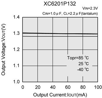
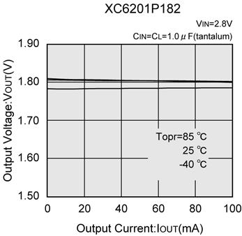
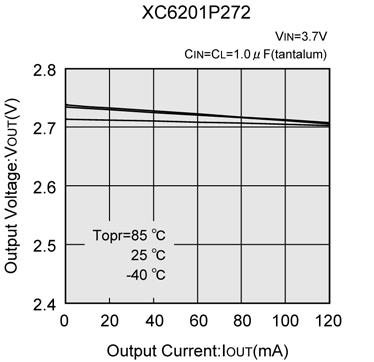
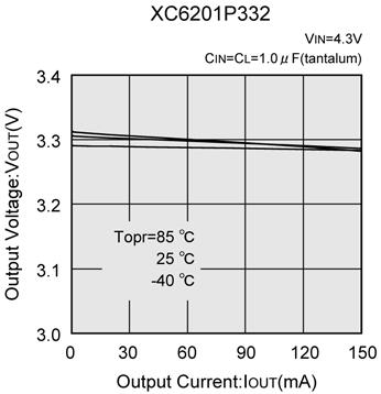
8 TYPICAL PERFORMANCE CHARACTERISTICS (1) Output Voltage vs. Output Current 8/24


9 XC6201 Series TYPICAL PERFORMANCE CHARACTERISTICS (Continued) (2) Output Voltage vs. Input Voltage XC6201P132 XC6201P132 XC6201P182 XC6201P182 XC6201P272 XC6201P272 9/24


 XC6201P332")
10 TYPICAL PERFORMANCE CHARACTERISTICS (Continued) (2) Output Voltage vs. Input Voltage (Continued) XC6201P332 XC6201P332 XC6201P502 XC6201P502 10/24


11 XC6201 Series TYPICAL PERFORMANCE CHARACTERISTICS (Continued) (3) Dropout Voltage vs. Output Current XC6201P132 XC6201P182 XC6201P272 XC6201P332 XC6201P502 11/24
12 TYPICAL PERFORMANCE CHARACTERISTICS (Continued) (4) Supply Current vs. Input Voltage XC6201P132 XC6201P132 XC6201P182 12/24

")
13 XC6201 Series TYPICAL PERFORMANCE CHARACTERISTICS (Continued) (4) Supply Current vs. Input Voltage (Continued) XC6201P332 13/24

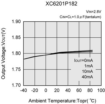
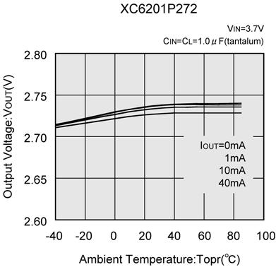
14 TYPICAL PERFORMANCE CHARACTERISTICS (Continued) (5) Output Voltage vs. Ambient Temperature 14/24

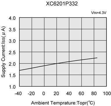
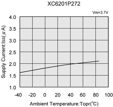
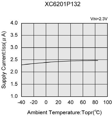
15 XC6201 Series TYPICAL PERFORMANCE CHARACTERISTICS (Continued) (6) Supply Current vs. Ambient Temperature 15/24
 (7) Input Transient")
 Time (1ms/div) XC6201P272")
 XC6201P502 Time (1ms/div)")
16 TYPICAL PERFORMANCE CHARACTERISTICS (Continued) (7) Input Transient Response XC6201P132 XC6201P182 Time (1ms/div) Time (1ms/div) XC6201P272 XC6201P332 Time (1ms/div) Time (1ms/div) XC6201P502 Time (1ms/div) 16/24

 (8) Load")

 XC6201P272")

17 XC6201 Series TYPICAL PERFORMANCE CHARACTERISTICS (Continued) (8) Load Transient Response XC6201P132 XC6201P182 Time (2ms/div) Time (2ms/div) XC6201P272 XC6201P332 Time (2ms/div) Time (2ms/div) XC6201P502 Time (2ms/div) 17/24

 (9)")


")
18 TYPICAL PERFORMANCE CHARACTERISTICS (Continued) (9) Ripple Rejection Rate XC6201P132 XC6201P182 XC6201P272 XC6201P332 XC6201P502 (10) Output Noise Density XC6201P302 18/24
19 XC6201 Series PACKAGING INFORMATION SOT-25 Unit : mm 2.9± ~ ± ± ± MAX 0.2MIN (0.95) SOT-89 Unit : mm 19/24
20 PACKAGING INFORMATION (Continued) TO-92 Paper type Unit : mm Bag Unit : mm USP-6B Unit : mm 20/24
21 XC6201 Series PACKAGING INFORMATION (Continued) USP-6B Reference Pattern Layout USP-6B Reference Metal Mask Design 21/24
22 MARKING RULE SOT-89, SOT represents the product series MARK PRODUCT SERIES 1 XC6201Pxxxxx SOT-89 (TOP VIEW) 2 represents type of regulator MARK VOLTAGE (V) ~ ~ SOT-25 (TOP VIEW) 3 represents output voltage MARK OUTPUT VOLTAGE (V) MARK OUTPUT VOLTAGE (V) F H K L M N P R S T A U B V C X D Y E Z represents assembly lot number 0 to 9, A to Z repeated (G, I, J, O, Q, W excluded) 22/24

23 XC6201 Series MARKING RULE (Continued) TO-92 1 represents type of regulator MARK P T PRODUCT SERIES XC6201Pxxxxx XC6201Txxxxx (SIDE VIEW) (SIDE VIEW) 23 represents output voltage MARK VOLTAGE (V) 2 3 PRODUCT SERIES XC6201Px33xx XC6201Px50xx 4 represents detect voltage accuracy MARK DETECT VOLTAGE ACCURACY PRODUCT SERIES MARK 1 Within ±1% XC6201Pxx1xx 2 Within ±2% XC6201Pxx2xx 5 represents least significant digit of production year PRODUCTION YEAR represents the production lot number 0 to 9, A to Z repeated (G, I, J, O, Q, W excluded) Note: No character inversion used. USP-6B USP-6B (TOP VIEW) 12 represents product series 1 MARK 2 PRODUCT SERIES 0 1 XC6201xxxxDx 3 represents type of regulator MARK TYPE PRODUCT SERIES 4 P 3pin Regulator XC6201PxxxDx T VIN=7V(Rated) XC6201TxxxDx 45 represents output voltage MARK 5 VOLTAGE (V) PRODUCT SERIES XC6201x33xDx XC6201x50xDx 6 represents assembly lot number 0 to 9, A to Z repeated (G, I, J, O, Q, W excluded) Note: No character inversion used. 23/24
24 1. The products and product specifications contained herein are subject to change without notice to improve performance characteristics. Consult us, or our representatives before use, to confirm that the information in this datasheet is up to date. 2. We assume no responsibility for any infringement of patents, patent rights, or other rights arising from the use of any information and circuitry in this datasheet. 3. Please ensure suitable shipping controls (including fail-safe designs and aging protection) are in force for equipment employing products listed in this datasheet. 4. The products in this datasheet are not developed, designed, or approved for use with such equipment whose failure of malfunction can be reasonably expected to directly endanger the life of, or cause significant injury to, the user. (e.g. Atomic energy; aerospace; transport; combustion and associated safety equipment thereof.) 5. Please use the products listed in this datasheet within the specified ranges. Should you wish to use the products under conditions exceeding the specifications, please consult us or our representatives. 6. We assume no responsibility for damage or loss due to abnormal use. 7. All rights reserved. No part of this datasheet may be copied or reproduced without the prior permission of TOREX SEMICONDUCTOR LTD. 24/24
XC6206 Series GENERAL DESCRIPTION FEATURES APPLICATIONS TYPICAL PERFORMANCE CHARACTERISTICS TYPICAL APPLICATION CIRCUIT 1/17
 ETR0305_004a GENERAL DESCRIPTION The XC6206 series are highly precise, low power consumption, 3 terminal, positive voltage regulators manufactured using CMOS and laser trimming technologies. The series
GENERAL DESCRIPTION FEATURES APPLICATIONS TYPICAL PERFORMANCE CHARACTERISTICS TYPICAL APPLICATION CIRCUIT 1/17. Battery powered equipment
 ETR0305_003a GENERAL DESCRIPTION The XC6206 series are highly precise, low power consumption, high voltage, positive voltage regulators manufactured using CMOS and laser trimming technologies. The series
GENERAL DESCRIPTION FEATURES APPLICATIONS TYPICAL PERFORMANCE CHARACTERISTICS TYPICAL APPLICATION CIRCUIT 1/17
 ETR0305_002 GENERAL DESCRIPTION The XC6206 series are highly precise, low power consumption, high voltage, positive voltage regulators manufactured using CMOS and laser trimming technologies. The series
XC62K Series GENERAL DESCRIPTION APPLICATIONS FEATURES TYPICAL PERFORMANCE CHARACTERISTICS TYPICAL APPLICATION CIRCUIT. Negative Voltage Regulators
 ETR0313_005 Negative Voltage Regulators GENERAL DESCRIPTION The XC62K series are highly precise, low power consumption, negative voltage regulators, manufactured using CMOS and laser trimming technologies.
PIN CONFIGURATION *The dissipation pad for the USP-6B package should be solder-plated in recommended mount pattern and metal masking so as to enhance
 ETR0305_004a GENERAL DESCRIPTION The XC6206 series are highly precise, low power consumption, 3 terminal, positive voltage regulators manufactured using CMOS and laser trimming technologies. The series
FEATURES Maximum Output Current APPLICATIONS. TYPICAL PERFORMANCE CHARACTERISTICS Supply Current vs. Input Voltage TYPICAL APPLICATION CIRCUIT 1/22
 ETR0329-005 GENERAL DESCRIPTION XC6218 series are highly precise, low noise, positive voltage LDO regulators manufactured using CMOS processes. The series achieves very low supply current, 1.0A (TYP.)
XC62K Series GENERAL DESCRIPTION APPLICATIONS FEATURES TYPICAL PERFORMANCE CHARACTERISTICS TYPICAL APPLICATION CIRCUIT. Negative Voltage Regulators
 ETR0313_006 Negative Voltage Regulators GENERAL DESCRIPTION The XC62K series are highly precise, low power consumption, negative voltage regulators, manufactured using CMOS and laser trimming technologies.
XC6210 Series APPLICATIONS. TYPICAL PERFORMANCE CHARACTERISTICS Dropout Voltage vs. Output Current TYPICAL APPLICATION CIRCUIT
 ETR0317_004 High Current, High Speed LDO Regulators GENERAL DESCRIPTION The XC6210 series are precise, low noise, high current, positive voltage low dropout regulators. They are fabricated using Torex
XC62H Series GENERAL DESCRIPTION APPLICATIONS FEATURES TYPICAL PERFORMANCE CHARACTERISTICS TYPICAL APPLICATION CIRCUIT
 ETR0312_006 Positive Voltage Regulator with (Output ON/OFF) GENERAL DESCRIPTION The XC62H series are highly precise, low power consumption, positive voltage regulators, manufactured using CMOS and laser
XC6202 Series GENERAL DESCRIPTION APPLICATIONS. FEATURES Maximum Output Current : 150mA (within Pd) Maximum Operational Voltage : 20V
 Maximum Operational Voltage : 20V") XC6 Series High Voltage Positive Voltage Regulators ETR3_7 GENERAL DESCRIPTION The XC6 series are highly precise, low power consumption, high voltage input, positive voltage regulators manufactured using
XC6 Series High Voltage Positive Voltage Regulators ETR3_7 GENERAL DESCRIPTION The XC6 series are highly precise, low power consumption, high voltage input, positive voltage regulators manufactured using
High Speed LDO Regulators Low ESR Cap.Compatible,Output ON/OFFControl
 ETR0306_005 High Speed LDO Regulators Low ESR Cap.Compatible,Output ON/OFFControl GENERAL DESCRIPTION The XC6209/XC6212 series are highly precise, low noise, positive voltage LDO regulators manufactured
XC6401 Series FEATURES
 XC1 Series ETR9_7 Dual LDO Regulators, Low ESR Cap. Compatible GENERAL DESCRIPTION The XC1 series are highly accurate, Dual, low noise, CMOS LDO voltage regulators. Performance features of the series includes
XC6214 Series. FEATURES Maximum Output Current APPLICATIONS. TYPICAL PERFORMANCE CHARACTERISTICS Dropout Voltage vs. Output Current XC6214P332
 XC6 Series ETR8_ ma Output Current, High Speed LDO Regulators, Thermal Shutdown Function, Ceramic Capacitor Compatible GENERAL DESCRIPTION The XC6 series are highly precise, low noise, high current, positive
APPLICATIONS. FEATURES Maximum Output Current : 200mA (300mA Limit, TYP.)
") Low Power Consumption:.8µA (TYP.) Range :.V ~.V Range :.9V ~.V Maximum Output Current: ma (ma Limit, TYP.) @ VOUT=.V, VIN=.V Current Limiter Circuit Built-In Ceramic Capacitor Compatible Small Packages
Low Power Consumption:.8µA (TYP.) Range :.V ~.V Range :.9V ~.V Maximum Output Current: ma (ma Limit, TYP.) @ VOUT=.V, VIN=.V Current Limiter Circuit Built-In Ceramic Capacitor Compatible Small Packages
XC6206 Series GENERAL DESCRIPTION FEATURES APPLICATIONS TYPICAL PERFORMANCE CHARACTERISTICS TYPICAL APPLICATION CIRCUIT 1/17
 ETR0305_007 GENERAL DESCRIPTION The XC6206 series are highly precise, low power consumption, 3 terminal, positive voltage regulators manufactured using CMOS and laser trimming technologies. The series
XC6210 Series APPLICATIONS. TYPICAL PERFORMANCE CHARACTERISTICS Dropout Voltage vs. Output Current TYPICAL APPLICATION CIRCUIT
 ETR317_6 High Current, High Speed LDO Regulators GENERAL DESCRIPTION The XC621 series are precise, low noise, high current, positive voltage low dropout regulators. They are fabricated using Torex s CMOS
High Speed LDO Regulators Low ESR Cap.Compatible,Output ON/OFFControl
 ETR0306_006 High Speed LDO Regulators Low ESR Cap.Compatible,Output ON/OFFControl GENERAL DESCRIPTION The XC6209/XC6212 series are highly precise, low noise, positive voltage LDO regulators manufactured
XC6401 Series FEATURES. TYPICAL PERFORMANCE CHARACTERISTICS Interactive Load Transient Response TYPICAL APPLICATION CIRCUITS
 XC Series ETR9_ Dual LDO Regulators, Low ESR Cap. Compatible GENERAL DESCRIPTION The XC series are highly accurate, Dual, low noise, CMOS LDO voltage regulators. Performance features of the series includes
APPLICATIONS Mobile Phones Cordless phones and radio communication equipment Portable games Cameras, Video recorders Portable Audio Equipment PDAs
 Low Power Consumption : μa (TYP.) Dropout Voltage : mv @ ma : mv @ma Range :.8V to.v Output Current : More than ma (ma limit) Low Output Noise High Ripple Rejection Rate Low ESR capacitor compatible GENERAL
200mA High Speed LDO Voltage Regulator with Inrush Current Prevention
 ETR03066-004 200mA High Speed LDO Voltage Regulator with Inrush Current Prevention GENERAL DESCRIPTION The XC6233 series is a 200mA high speed LDO regulator that features high accurate high ripple rejection
XC6234 Series APPLICATIONS TYPICAL APPLICATION CIRCUIT TYPICAL PERFORMANCE CHARACTERISTICS. 200mA High Speed LDO Regulator with ON/OFF Switch 1/23
 ETR367-2 ma High Speed LDO Regulator with ON/OFF Switch GENERAL DESCRIPTION The series is a ma high speed LDO regulator that features high accurate, high ripple rejection and low dropout. The series consists
APPLICATIONS Mobile phones Cordless phones Cameras, video recorders Portable games Portable AV equipment Reference voltage Battery powered equipment
 CMOS Low Power Consumption Dropout Voltage : 60mV @ 30mA 200mV @ 100mA Maximum Output Current : 150mA (300mA=XC6204 E to H Type) Highly Accurate : ±2% Output Voltage Range : 1.8V ~ 6.0V (XC6204) 0.9V ~
300mA/150mA High Speed LDO Regulators with ON-OFF Control
 ETR03004-010 300mA/150mA High Speed LDO Regulators with ON-OFF Control GENERAL DESCRIPTION The XC6204/XC6205 series are highly precise, low noise, positive voltage LDO regulators manufactured using CMOS
Highly Accurate, Ultra Small, Low Power Consumption Voltage Detector
 ETR0209-004 Highly Accurate, Ultra Small, Low Power Consumption Voltage Detector GENERAL DESCRIPTION The XC6120 series are highly precise, low power consumption voltage detectors, manufactured using CMOS
XB1117 Series APPLICATIONS. FEATURES Maximum Output Current TYPICAL PERFORMANCE CHARACTERISTICS TYPICAL APPLICATION CIRCUIT
 ETR0315_006 1A Low Dropout Positive oltage Regulator GENERAL DESCRIPTION The XB1117 series is 1A Bi-polar transistor LDO voltage regulator. Output voltage of the XB1117P series is fixed to 1.8, 2.5, 3.3,
XB1086 Series GENERAL DESCRIPTION FEATURES APPLICATIONS TYPICAL APPLICATION CIRCUITS TYPICAL PERFORMANCE CHARACTERISTICS
 XB086 Series ETR0325-008.5A Positive Voltage Regulator GENERAL DESCRIPTION The XB086 is a series of low dropout positive voltage regulators with a high output current capability of.5a. Stable output can
XB1085 Series GENERAL DESCRIPTION FEATURES APPLICATIONS. TYPICAL PERFORMANCE CHARACTERISTICS Output Voltage vs. Output Current
 XB085 Series ETR0324-008 3.0A Positive Voltage Regulator GENERAL DESCRIPTION The XB085 is a series of low dropout positive voltage regulators with a high output current capacity of 3.0A. Stable output
28 V Input High Speed Voltage Regulator
 28 V Input High Speed Voltage Regulator FEATURES Operating Voltage Range 2.0 V 28.0 V Output Voltage Range from 1.8 V to 18.0 V with 0.1 V increments Output Voltage Accuracy ± 2% Temperature Stability
PWM,PWM/PFM Switching Step-Up & Down DC/DC Converter Controller ICs
 ETR0601_001c PWM,PWM/PFM Switching Step-Up & Down DC/DC Converter Controller ICs GENERAL DESCRIPTION Green Operation Compatible The XC9301/XC9302 series are step-up/down DC/DC converter controller ICs
XCM410 Series. FEATURES High Accuracy APPLICATIONS TYPICAL APPLICATION CIRCUIT. 2 Channel Voltage Detector (Sense Pin separated from V DD ) 1/13
 1/13") ETR2426_003 2 Channel Voltage Detector (Sense Pin separated from V DD ) GENERAL DESCRIPTION The XCM410 series is a multi combination module IC which comprises of two voltage detectors, XC6108 and XC6109
ETR2426_003 2 Channel Voltage Detector (Sense Pin separated from V DD ) GENERAL DESCRIPTION The XCM410 series is a multi combination module IC which comprises of two voltage detectors, XC6108 and XC6109
XC6119 Series. FEATURES High Accuracy : +2% APPLICATIONS TYPICAL PERFORMANCE CHARACTERISTICS TYPICAL APPLICATION CIRCUIT
 XC69 Series ETR0206-00 Voltage Detector with Delay Time Adjustable GENERAL DESCRIPTION The XC69 series is a highly precise, low power consumption voltage detector, manufactured using CMOS and laser trimming
XC6504 Series. APPLICATIONS Mobile devices / terminals Wireless LAN Modules (wireless, cameras, etc.) TYPICAL PERFORMANCE CHARACTERISTICS
 TYPICAL PERFORMANCE CHARACTERISTICS") XC654 Series ETR47-7.6μA Ultra Low Power Consumption Small Voltage Regulator (CL Capacitor-Less) GENERAL DESCRIPTION The XC654 series is a highly accurate CMOS voltage regulator that achieves very low
XC654 Series ETR47-7.6μA Ultra Low Power Consumption Small Voltage Regulator (CL Capacitor-Less) GENERAL DESCRIPTION The XC654 series is a highly accurate CMOS voltage regulator that achieves very low
A6304A. AiT Semiconductor Inc. APPLICATION ORDERING INFORMATION TYPICAL APPLICATION
 DESCRIPTION The series are highly precise, low noise, positive voltage LDO regulators manufactured using CMOS processes. The series achieves high ripple rejection and low dropout and consists of a standard
High Current, High Speed LDO Regulators, Voltage Detector Function
 ETR1004-006 High Current, High Speed LDO Regulators, Voltage Detector Function GENERAL DESCRIPTION The XC6413/XC6414 series are highly precise, low noise, positive voltage LDO regulators with voltage detector
28 V, 150 ma Voltage Regulator with Stand-by Mode
 28 V, 150 ma Voltage Regulator with Stand-by Mode FEATURES Operating Voltage Range 2.0 V 28.0 V Output Voltage Range from 2.0 V to 12.0 V with 0.1 V increments (B series) or 2.0 V 23 V with external resistors
XC61C Series GENERAL DESCRIPTION
 ETR1_16 Low Voltage Detectors (VDF=.8V~1.V) Standard Voltage Detectors (VDF 1.6V~6.V) GENERAL DESCRIPTION The XC61C series are highly precise, low power consumption voltage detectors, manufactured using
XC6215 Series FEATURES APPLICATIONS TYPICAL APPLICATION CIRCUIT TYPICAL PERFORMANCE CHARACTERISTICS
 XC Series ETR9_.8μA Low Power Consumption Voltage Regulator with ON/OFF Switch GENERAL DESCRIPTION The XC series are highly precise, low noise, positive voltage LDO regulators manufactured using CMOS processes.
XC61F Series GENERAL DESCRIPTION APPLICATIONS
 ETR0202-007a Voltage Detectors, Delay Circuit Built-In GENERAL DESCRIPTION The XC61F series are highly accurate, low power consumption voltage detectors, manufactured using CMOS and laser trimming technologies.
Built-in Inrush Current Protection, 300mA High Speed LDO Voltage Regulator
 XC6223 Series ETR339-5 Built-in Inrush Current Protection, 3mA High Speed LDO Voltage Regulator GENERAL DESCRIPTION The XC6223 series is a high speed LDO regulator that features high accurate, low noise,
XC2163 Series GENERAL DESCRIPTION APPLICATIONS FEATURES PIN ASSIGNMENT PIN CONFIGURATION /INH, Q0 PIN FUNCTION
 ETR1403_001a ICs for use with 3rd Overtone Crystal Oscillators GENERAL DESCRIPTION The XC2163 series are high frequency, low current consumption CMOS ICs with built-in crystal oscillator and divider circuits.
XC2300 Series GENERAL DESCRIPTION APPLICATIONS FEATURES PIN CONFIGURATION PIN ASSIGNMENT /INH, Q0 PIN FUNCTION. Tri-State Buffer ICs 1/7
 ETR1406_001a Tri-State Buffer ICs GENERAL DESCRIPTION The 2300 Series are a group of high frequency, CMOS low power tri-state buffer ICs with input amplifier, divider and output tri-state buffer circuits
XC8102 Series FEATURES APPLICATIONS TYPICAL PERFORMANCE CHARACTERISTICS TYPICAL APPLICATION CIRCUIT
 ETR2502-012 Load Switch with Low On-Resistance (Current Limit 400mA) GENERAL DESCRIPTION The XC8102 series is a low ON resistance load switch IC with ON/OFF control and output current protection which
XC9253R Series TYPICAL APPLICATION CIRCUIT. Synchronous Step-Down DC/DC Converter 1/13. GreenOperation Compatible
 ETR0528_003 Synchronous Step-Down DC/DC Converter GreenOperation Compatible GENERAL DESCRIPTION The series is a group of synchronous-rectification type DC/DC converters with a built-in 0.6P-channel driver
LOW ESR Cap. Compatible Positive Voltage Regulators XC6206 Series
 SOT-23 Unit: mm Features Maximum Output Current : 200mA Dropout Voltage : 250mV (IOUT = 100mA) Maximum Operating Voltage : 6V Output Voltage Range : 1.2V ~ 5V (0.1V increments) Highly Accurate : ±2%@VOUT
High Speed Low Dropout Middle Current Voltage Regulators. Designator Symbol Description Designator Symbol Description CE Pin Logic :
 High Speed Low Dropout Middle Current Voltage Regulators General Description The series are highly precise, low noise, positive voltage LDO regulators manufactured using CMOS processes. The series achieves
XC9801/XC9802 Series GENERAL DESCRIPTION FEATURES APPLICATIONS TYPICAL APPLICATION CIRCUIT TYPICAL PERFORMANCE CHARACTERISTICS
 XC9801/XC9802 Series ETR0804-006 Regulated Voltage Step-Up Charge Pump ICs GENERAL DESCRIPTION The XC9801 series are fixed regulated voltage step-up charge pump ICs which provide stable, highly efficient,
Dual LDO Regulator (ch1: 300mA, ch2: 100mA) with ON/OFF Switch
 with ON/OFF Switch") XC6419 Series ETR338-5 Dual LDO Regulator (ch1: 3mA, ch2: 1mA) with ON/OFF Switch GENERAL DESCRIPTION The XC6419 series is a dual CMOS LDO regulator. The series features high accuracy, low output noise,
XC6419 Series ETR338-5 Dual LDO Regulator (ch1: 3mA, ch2: 1mA) with ON/OFF Switch GENERAL DESCRIPTION The XC6419 series is a dual CMOS LDO regulator. The series features high accuracy, low output noise,
XC6901 Series APPLICATIONS TYPICAL PERFORMANCE CHARACTERISTICS TYPICAL APPLICATION CIRCUIT. 200mA Negative Voltage Regulator with ON/OFF Control 1/28
 XC691 Series ETR343-7 2mA Negative Voltage Regulator with ON/OFF Control GENERAL DESCRIPTION The XC691 Series is a negative voltage CMOS regulator which includes a reference voltage source, error amplifier,
XP151A13A0MR-G GENERAL DESCRIPTION
 ETR1119_003 Power MOSFET GENERAL DESCRIPTION The XP151A13A0MR-G is an N-channel Power MOSFET with low on state resistance and ultra high-speed switching characteristics. Because high-speed switching is
600mA Driver Tr. Built-In, Synchronous Step-Down DC/DC Converter
 XC9254R Series ETR0529-003 600mA Driver Tr. Built-In, Synchronous Step-Down DC/DC Converter GreenOperation Compatible GENERAL DESCRIPTION The XC9254R series is a group of synchronous-rectification type
XP162A11C0PR-G GENERAL DESCRIPTION
 ETR1125_003 Power MOSFET GENERAL DESCRIPTION The XP162A11C0PR-G is a P-channel Power MOSFET with low on-state resistance and ultra high-speed switching characteristics. Because high-speed switching is
Ultra Small Analog Output Temperature Sensor with Alarm Output Pin
 ETR0902-005 Ultra Small Analog Output Temperature Sensor with Alarm Output Pin GENERAL DESCRIPTION The XC3101 series is a temperature sensor IC which features ultra small, low current consumption, and
XP152A11E5MR-G GENERAL DESCRIPTION
 ETR1120_003 Power MOSFET GENERAL DESCRIPTION The XP152A11E5MR-G is a P-channel Power MOSFET with low on-state resistance and ultra high-speed switching characteristics. Because high-speed switching is
*1. Attention should be paid to the power dissipation of the package when the load is large.
 Rev.3._ HIGH RIPPLE-REJECTION LOW DROPOUT CMOS VOLTAGE REGULATOR Features The S-L298 series is a positive voltage regulator with a low dropout voltage, high output voltage accuracy, and low current consumption
XP161A1355PR-G GENERAL DESCRIPTION. FEATURES Low On-State Resistance : Rds (on)= Vgs = 4.5V APPLICATIONS PRODUCT NAME
= Vgs = 4.5V APPLICATIONS PRODUCT NAME") ETR1124_003 Power MOSFET GENERAL DESCRIPTION The XP161A1355PR-G is an N-channel Power MOSFET with low on-state resistance and ultra high-speed switching characteristics. Because high-speed switching is
ETR1124_003 Power MOSFET GENERAL DESCRIPTION The XP161A1355PR-G is an N-channel Power MOSFET with low on-state resistance and ultra high-speed switching characteristics. Because high-speed switching is
PWM Controlled, PWM/PFM Switchable Step-up DC/DC Controllers
 XC6367/XC6368 Series ETR0401_005 PWM Controlled, PWM/PFM Switchable Step-up DC/DC Controllers GreenOperation-Compatible GENERAL DESCRIPTION The XC6367/XC6368 series are multi-functional step-up DC/DC controllers
ACE507A. Precise Low Dropout Voltage Regulator. Description. Features. Application. Functional Block Diagram
 Description The series are precise, low power consumption; positive voltage regulators manufactured using CMOS and laser trimming technologies. The series provides large currents with a significantly small
1.5 V to 5.5 V, selectable in 0.1 V step Output voltage accuracy:
 www.ablicinc.com HIGH RIPPLE-REJECTION LOW DROPOUT CMOS VOLTAGE REGULATOR ABLIC Inc., 23-215 Rev.3.1_2 The is a positive voltage regulator with a low dropout voltage, high-accuracy output voltage, and
XC9119D10A Series APPLICATIONS TYPICAL APPLICATION CIRCUIT. TYPICAL PERFORMANCE CHARACTERISTICS Efficiency vs. Output Current
 XC9119D1A Series ETR48_9 1MHz, PWM Controlled, Step-Up DC/DC Converter, Ceramic Capacitor Compatible GENERAL DESCRIPTION The XC9119D1A series is 1MHz, PWM controlled step-up DC/DC converter, designed to
*1. Attention should be paid to the power dissipation of the package when the load is large. *2. Refer to Product Name Structure for details.
 www.sii-ic.com HIGH RIPPLE-REJECTION AND LOW DROPOUT CMOS VOLTAGE REGULATOR Seiko Instruments Inc., 21-21 Rev.5._ The S-L298 series is a positive voltage regulator with a low dropout voltage, high output
PT7M8205 LDO Regulator
 Features Output Current: 300mA or more Dropout Voltage: 270mV @ 300mA for 3.3V Operating Voltage Range: 1.8 to 5.5V Output Voltage Range: 1.2 to 3.3V (100mV Step) Low Power Consumption: 65µA High Ripple
28V Low Power Consumption 150mA Voltage Regulators (with Stand-by Function)
") XC/XE Series ETR_ V Low Power Consumption ma Voltage Regulators (with Stand-by Function) GENERAL DESCRIPTION XC/XE series are positive voltage regulator ICs with V of operation voltage. The series consists
XC/XE Series ETR_ V Low Power Consumption ma Voltage Regulators (with Stand-by Function) GENERAL DESCRIPTION XC/XE series are positive voltage regulator ICs with V of operation voltage. The series consists
HIGH RIPPLE-REJECTION LOW DROPOUT LOW INPUT-AND-OUTPUT CAPACITANCE CMOS VOLTAGE REGULATOR
 Rev.3.2_ HIGH RIPPLE-REJECTION LOW DROPOUT LOW INPUT-AND-OUTPUT CAPACITANCE CMOS VOLTAGE REGULATOR S-12 Series The S-12 Series is a positive voltage regulator with a low dropout voltage, high output voltage
STL6341. Low IQ Regulator. 100mA Ultra Low Quiescent Current Linear Regulator DESCRIPTION FEATURE APPLICATIONS PIN CONFIGURATION
 DESCRIPTION The series is a positive voltage regulator with high accuracy output voltage and ultra-low quiescent current which is typically 1.0μA. The device is ideal for battery powered handheld equipments
VRR Series. AnaSem. High speed, Low dropout, ±1% High output accuracy CMOS Voltage Regulator with On/Off circuit. Analog Semiconductor IC. AnaSem Inc.
 AnaSem Analog Semiconductor IC High speed, Low dropout, ±% High output accuracy CMOS Voltage Regulator with On/Off circuit Rev. E9- Rev. E9- AnaSem Products Data Sheet Analog Semiconductor IC High speed,
XP202A0003MR-G FEATURES APPLICATIONS PRODUCT NAME PIN CONFIGURATION ABSOLUTE MAXIMUM RATINGS ELECTRICAL CHARACTERISTICS. P-channel 4V (G-S) MOSFET 1/5
 MOSFET 1/5") -G ETR28 P-channel 4V (G-S) MOSFET FEATURES Low On Resistance Ultra High Speed Switching V Driving EU RoHS Compliant, Pb Free ABSOLUTE MAXIMUM RATINGS APPLICATIONS Switching PRODUCT NAME PRODUCT NAME PACKAGE
-G ETR28 P-channel 4V (G-S) MOSFET FEATURES Low On Resistance Ultra High Speed Switching V Driving EU RoHS Compliant, Pb Free ABSOLUTE MAXIMUM RATINGS APPLICATIONS Switching PRODUCT NAME PRODUCT NAME PACKAGE
XC9110/XC9111 Series GENERAL DESCRIPTION APPLICATIONS FEATURES TYPICAL APPLICATION CIRCUIT. PFM Controlled Step-Up DC/DC Converter / Controller ICs
 XC911/XC9111 Series ETR46-6a PFM Controlled Step-Up DC/DC Converter / Controller ICs GENERAL DESCRIPTION The XC911/9111 series is a group of PFM controlled step-up DC/DC converter/controller ICs designed
XC6901 Series APPLICATIONS TYPICAL PERFORMANCE CHARACTERISTICS TYPICAL APPLICATION CIRCUIT. 200mA Negative Voltage Regulator with ON/OFF Control 1/28
 ETR343-6 2mA Negative Voltage Regulator with ON/OFF Control GENERAL DESCRIPTION The is a negative voltage CMOS regulator which includes a reference voltage source, error amplifier, driver transistor, current
Ultra Small, Low Power Consumption Voltage Detector
 Ultra Small, Low Power Consumption Voltage Detector FEATURES Accuracy ± 2% at V DF 1.5 V or ±0.03 V Low Power Consumption at 0.6 μa typical at V DF = 2.7 V, V IN = 2.97 V Detect Voltage Range 0.7 V 5.0
S-L2980 Series HIGH RIPPLE-REJECTION AND LOW DROPOUT CMOS VOLTAGE REGULATOR. Features. Applications. Package
 www.ablicinc.com HIGH RIPPLE-REJECTION AND LOW DROPOUT CMOS VOLTAGE REGULATOR ABLIC Inc., 21-212 Rev.5.1_2 The is a positive voltage regulator with a low dropout voltage, high output voltage accuracy,
VRD Series. AnaSem. High speed, Low dropout, ±1% High output accuracy CMOS Voltage Regulator with Dual output. Analog Semiconductor IC.
 安纳森 Analog Semiconductor IC High speed, Low dropout, ±% High output accuracy CMOS Voltage Regulator with Dual output (IMPORTANT: Please check the last page for Genuine Product Labeling) Rev. E- Website:
Low Quiescent Current_Low Dropout CMOS Voltage Regulator
 Low Quiescent _Low Dropout CMOS Voltage Regulator HM53XX Series 500mA Ferture: high output accuracy ±2% low dropout 1.5mV Iout=1mA low quiescent current Max input Output current Applications ⒈2uA 10V 500mA
VRH Series. AnaSem. High speed, Low dropout, ±1% High output accuracy CMOS Voltage Regulator with On/Off circuit. Analog Semiconductor IC.
 安纳森 Analog Semiconductor IC High speed, Low dropout, ±% High output accuracy CMOS Voltage Regulator with On/Off circuit (IMPORTANT: Please check the last page for Genuine Product Labeling) Rev. E- Website:
1.5 V to 5.5 V, selectable in 0.1 V step Output voltage accuracy: ±1.0% Dropout voltage:
 www.sii-ic.com HIGH RIPPLE-REJECTION LOW DROPOUT CMOS VOLTAGE REGULATOR Seiko Instruments Inc., 22-215 Rev.5.1_ The is a positive voltage regulator with a low dropout voltage, high-accuracy output voltage,
1.5 V to 5.5 V, selectable in 0.1 V step
 S-1167 Series www.ablicinc.com ULTRA LOW CURRENT CONSUMPTION, HIGH RIPPLE REJECTION AND LOW DROPOUT CMOS VOLTAGE REGULATOR ABLIC Inc., 24-215 Rev.3.2_2 The S-1167 Series is a positive voltage regulator
HIGH RIPPLE-REJECTION LOW DROPOUT MIDDLE OUTPUT CURRENT CMOS VOLTAGE REGULATOR
 Rev.2.3_ HIGH RIPPLE-REJECTION LOW DROPOUT MIDDLE OUTPUT CURRENT CMOS VOLTAGE REGULATOR S-1131 Series The S-1131 Series is a positive voltage regulator with a low dropout voltage, high output voltage accuracy,
High Ripple-Rejection Low Dropout CMOS Voltage Regulator
 High Ripple-Rejection Low Dropout CMOS Voltage Regulator General Description The Series is a positive voltage regulator with a low dropout voltage, high output voltage accuracy, and low current consumption
PT7M8206 LDO Regulator
 Features Output Current: 300mA or more Dropout Voltage: 270mV @ 300mA for 3.3V Operating Voltage Range: 1.8 to 5.5V Output Voltage Range: 1.2 to 3.3V (100mV Step) Low Power Consumption: 65µA Standby Current:
SOT-23-5, 5-Pin SON(A) *1. Attention should be paid to the power dissipation of the package when the output current is large.
 *1. Attention should be paid to the power dissipation of the package when the output current is large.") Rev.2.2_ HIGH RIPPLE-REJECTION LOW DROPOUT CMOS VOLTAGE REGULATOR The is a positive voltage regulator with a low dropout voltage, high output voltage accuracy, and low current consumption developed based
Rev.2.2_ HIGH RIPPLE-REJECTION LOW DROPOUT CMOS VOLTAGE REGULATOR The is a positive voltage regulator with a low dropout voltage, high output voltage accuracy, and low current consumption developed based
TX mA Low Power LDO
 Features Low power consumption Low Quiescent Current: 5.5uA at 6V Low voltage drop Output voltage accuracy: tolerance ±2% Low temperature coefficient Applications Battery-powered equipment Portable AV
PT7M8205 LDO Regulator
 PT7M8205 Features Output Current: 300mA or more Dropout Voltage: 270mV @ 300mA for 3.3V Operating Voltage Range: 1.8 to 5.5V Output Voltage Range: 1.2 to 3.3V (100mV Step) Low Power Consumption: 65A High
1.5 V to 5.5 V, selectable in 0.1 V step Output voltage accuracy: 140 mv typ. (3.0 V output product, I OUT = 200 ma)
") S-1165 Series www.ablicinc.com HIGH RIPPLE-REJECTION LOW DROPOUT CMOS VOLTAGE REGULATOR ABLIC Inc., -15 Rev.4.1_ The S-1165 Series is a positive voltage regulator with a low dropout voltage, high-accuracy
S-1165 Series www.ablicinc.com HIGH RIPPLE-REJECTION LOW DROPOUT CMOS VOLTAGE REGULATOR ABLIC Inc., -15 Rev.4.1_ The S-1165 Series is a positive voltage regulator with a low dropout voltage, high-accuracy
S-1132 Series HIGH RIPPLE-REJECTION AND LOW DROPOUT MIDDLE OUTPUT CURRENT CMOS VOLTAGE REGULATOR. Features. Applications. Packages.
 S-1132 Series www.ablicinc.com HIGH RIPPLE-REJECTION AND LOW DROPOUT MIDDLE OUTPUT CURRENT CMOS VOLTAGE REGULATOR ABLIC Inc., 24-215 Rev.4.2_2 The S-1132 Series is a positive voltage regulator with a low
CYStech Electronics Corp.
 Page No. : 1/10 Low Dropout CMOS Voltage Regulators SOT-23 Product Description The series is a set of three-terminal high current low voltage regulator implemented in CMOS technology. They can deliver
I/O Name Descriptions
 Features Output Current: 300mA or more Dropout Voltage: 270mV @ 300mA for 3.3V Operating Voltage Range: 1.8V to 5.5V Output Voltage Range: 1.2V to 3.3V (100mV Step) Low Power Consumption: 65 A Standby
A6251 LOW DROPOUT VOLTAGE REGULATOR 250mA, LOW POWER CONSUMPTION LDO
 DESCRIPTION The series are a group of positive voltage output, three pin regulator, that provide a high current even when the input/output Voltage differential is small. Low power consumption and high
LN809. Voltage Detectors With Delay Circuit Built-In. General Description. Applications. Features. Ordering Information
 Voltage Detectors With Delay Circuit Built-In General Description The is a cost-effective system supervisor Integrated Circuit (IC) designed to monitor VCC in digital and mixed signal systems and provide
STL6118A. Low Dropout Regulator. 300mA Low Dropout Low Noise LDO DESCRIPTION FEATURE APPLICATIONS PIN CONFIGURATION PART MARKING INFORMATION
 DESCRIPTION The series is a low dropout, low noise, low quiescent current linear regulator that operations in the input voltage range from +2.2V to +7.0V and delivers 300mA output current. The high-accuracy
JC6353V2.02. Description. Features. Application. Typical Application Circuits. 450mA ULTRA LOW DROPOUT POSITIVE VOLTAGE REGULATOR
 Description JC6353 series is a group of positive voltage output, three-pin regulators, that provide a high current even when the input/output voltage differential is small. Low power consumption and high
16V Input Voltage Step-Down DC/DC Controller
 16V Input Voltage Step-Down DC/DC Controller FEATURES Operating Input Voltage Range: 2.8V ~ 16.0V Output Voltage Range Externally Set: > 1.2V Output Current: up to 3A Reference Voltage: 0.9V ± 1.5% Oscillation
60 db typ. (1.25 V output product, f = 1.0 khz) Built-in overcurrent protection circuit: Limits overcurrent of output transistor.
 Built-in overcurrent protection circuit: Limits overcurrent of output transistor.") www.ablicinc.com S-11L1 Series 3.65 V INPUT, 15 ma, LOW OUTPUT VOLTAGE (.8 V) VOLTAGE REGULATOR ABLIC Inc., 29-217 Rev.2.3_1 The S-11L1 Series, developed by using the CMOS technology, is a positive voltage
www.ablicinc.com S-11L1 Series 3.65 V INPUT, 15 ma, LOW OUTPUT VOLTAGE (.8 V) VOLTAGE REGULATOR ABLIC Inc., 29-217 Rev.2.3_1 The S-11L1 Series, developed by using the CMOS technology, is a positive voltage
Low Voltage Input LDO Voltage Regulator with Soft-Start Function
 XC66 Series ETR5_7 Low Voltage Input LDO Voltage Regulator with Soft-Start Function GENERAL DESCRIPTION The XC66 series is a low voltage input CMOS LDO regulator which provides highly accurate (±mv) outputs
LOW DROPOUT CMOS VOLTAGE REGULATOR S-818 Series
 Rev.1.2 LOW DROPOUT CMOS VOLTAGE REGULATOR The is a positive voltage regulator developed utilizing CMOS technology featured by low dropout voltage, high output voltage accuracy and low current consumption.
load of 1µA ! Applications
 The S-817 is an ultra compact 3-pin positive voltage regulator developed using CMOS technology. Due to housing into an even more miniaturized SC-82AB package of 2. x 2.1 mm, the S-817 offers key advantages
1.5 V to 5.5 V, selectable in 0.1 V step Output voltage accuracy:
 S-117 Series www.ablicinc.com HIGH RIPPLE-REJECTION AND LOW DROPOUT HIGH OUTPUT CURRENT CMOS VOLTAGE REGULATOR ABLIC Inc., 23-215 Rev.4.1_2 The S-117 Series is a positive voltage regulator with a low dropout
XC6602 Series. APPLICATIONS Smart phones / Mobile phones. FEATURES Maximum Output Current : 1A (1.3A Limit)
") XC66 Series ETR35 A,.5V Low Input Voltage, High Speed LDO Regulator GENERAL DESCRIPTION The XC66 series is a low voltage input (.5V) operation and provides high accuracy ±5mV/±mV and can supply large current
XC66 Series ETR35 A,.5V Low Input Voltage, High Speed LDO Regulator GENERAL DESCRIPTION The XC66 series is a low voltage input (.5V) operation and provides high accuracy ±5mV/±mV and can supply large current
Fast Ultra High-PSRR, Low-Noise, 300mA CMOS Linear Regulator. Features
 Fast Ultra High-PSRR, Low-Noise, 300mA CMOS Linear Regulator General Description The features ultra-high power supply rejection ratio, low output voltage noise, low dropout voltage, low quiescent current
Ultra High-PSRR, Low-Noise, 300mA CMOS Linear Regulator. Applications. g g g g g g. Features
 Ultra High-PSRR, Low-Noise, 300mA CMOS Linear Regulator General Description Applications The features ultra-high power supply rejection ratio, low output voltage noise, low dropout voltage, low quiescent
HIGH RIPPLE-REJECTION LOW DROPOUT MIDDLE OUTPUT CURRENT CMOS VOLTAGE REGULATOR
 Rev.3._1 HIGH RIPPLE-REJECTION LOW DROPOUT MIDDLE OUTPUT CURRENT CMOS VOLTAGE REGULATOR S-1131 Series The S-1131 Series is a positive voltage regulator with a low dropout voltage, high output voltage accuracy,
70 db typ. (1.0 V output product, f = 1.0 khz) Built-in overcurrent protection circuit: Limits overcurrent of output transistor.
 Built-in overcurrent protection circuit: Limits overcurrent of output transistor.") S-1155 Series www.ablicinc.com HIGH RIPPLE-REJECTION LOW DROPOUT HIGH OUTPUT CURRENT CMOS VOLTAGE REGULATOR ABLIC Inc., 7-15 Rev..1_3 The S-1155 Series, developed by using CMOS technology, is a positive
S-1155 Series www.ablicinc.com HIGH RIPPLE-REJECTION LOW DROPOUT HIGH OUTPUT CURRENT CMOS VOLTAGE REGULATOR ABLIC Inc., 7-15 Rev..1_3 The S-1155 Series, developed by using CMOS technology, is a positive