Unipolar transistors measurement
|
|
|
- Kristian Webb
- 5 years ago
- Views:
Transcription

1 Unipolar transistors measurement 1. Important notice for students: Transistor s circuits works with frequency till hundredths MHz. For these frequency the interconnecting wires creates significant unwanted inductive and capacitive bindings, which cause oscillation of circuits. Oscillations are near limit values of V and I and disallow measurement of static characteristic, setting working points of amplifiers etc. Better, than using any RC filters is using suitable wiring. Solution is to prevent the rise of inductive loops. There exists simple rule. Each current have to return along the same way where to go there. This can be simply realised, when we twist connecting leads to measurement devices as A-meters V-meter. Powering of measuring kit uses flat double wire cable and scope probes uses coaxial cable connection. Better, than twisted pair wires, is coaxial cable, worse is flat double cable. Free non-arranged connection, realised according scheme, without its understanding is in communication, digital and power converter electronic functional nonsense. You should ensure that the area between free ends of connection leads must be minimal. Right example of connection of kit with transistor measurement is on following figure. 2. Important notice for students and teachers: Please, don t forget switch off multi-meters after measurement battery cells are expensive.
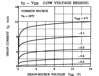
2 1. Measurement of static characteristics of Unipolar transistor N-MOS - type BS 107 or J-FET - type 2SK170 Task: 1) Measure dependence i C = f(u C, u G ) for given MOS or J FET transistor (N-channel). Plot the graphs. 2) Find transconductance (mutual conductance) y 21 and output admitance y 22 of transistor in working point according teachers instructions: v G =... V, v C =... (individual, as per teacher) i C i C y21 for vc 0 y22 for vg 0 v G v k Connection diagram for measurement output characteristic of N-MOS transistor. Table example for measured values of transistor characteristic: for BS107 select u g near +2V for 2SK170 select u g near +0,5V in such range, to be for v C = 10V i C in steps of 2mA from 0 to max 16 ma. u g V 0,5 1 2 u C V 3 i k ma BE CAREFULL! DO NOT OVERLOAD THE LIMIT HEAT DISSIPATION P Cmax = U C.I C
3 Parameter transistor limits: These valuet mustn t be in any case exceeded! BS107 (unip. transistor MOS-FET, N-channel): U C max = 200 V, I C max = 250 ma, P C max = 0,35 W 2SK170 (unip. transistor J-FET, N-channel): U C max = 60 V, I C max = 150 ma, P C max = 0,35 W Maximal power dissipation P Cmax = U C.I C in any measured point. During measurement limit P C <= 0,25W, e.g. I K <=20mA for V CE = 12V BS107, 2SK 170 Bottom terminal view D... drain... C collector G... gate... G gate S... source... E emitter 2. Measurement and calculation of transistor amplifier with N-MOS transistor. Connection diagram:
4 Measurement task: For all of A, B, C circuits (or according teacher instructions) do: 1) Connect given R K and R E into the kit and connect power supply. 2) Using potentiometer P working point, given by voltage between collector and emitter of transistor e.g. U CO = 5V (or U CO = 6V or U CO = 4V, according teachers instructions for all connections). In advance by calculation find current I CO and dissipation power P Cmax = U Co. I Co and verify, that it is less than 0,25 W. 3) Next to setting working point connect on input voltage v 1 of rectangular waveform of frequency cca. 1 khz from internal kit generator. Peak to peak voltage on input v 1 and voltage on output v 2 read using scope. Calculate amplifying coefficient A u using ratio v 2 and v 1 v2 A v v1 Tasks for calculations: For all of A, B, C connection do: 1) For given values of U A, R C, R E plot into diagram: Load line p, Dynamic transfer characteristic i C = f(v G ) Voltage transfer characteristic v C = g(v G ) 2) Plot into diagram working point P for given value of U CO (e.g. U CO = 5 V). And find : a) static values of v co, u go b) parameters y 21, y 22. c) dynamic transconductance S d d) Voltage amplifying coefficient A u 3) By calculations verify S d and A v using y 21, y 22. 4) Results of measurement and calculation compare and evaluate.

5 Possible combinations of parts (teacher can set another combination) U A = 12V (according power source on working place) connection A connection B connection C verse I II III IV I II III IV I II III IV R C [ ] 1k 2k2 1k 2k2 1k 2k2 1k 2k R E [ ] k 1k 2k2 1k 2k2 U C0 [V] Measurement of inverter Measure dependence v 2 = f (v 1 ) - transfer characteristic of inverter for BS107 and 2SK170 if enough time I II III IV R C [ ] 1k 2k2 1k 2k2 R 1 [ ] 10k M1 10k M1 R 1 [ ] k M1
6 DESIGN CATALOGUES DUMP:
7
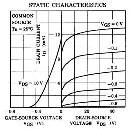
8 Static characteristic for 2SK J-FET:
ENEE307 Lab 7 MOS Transistors 2: Small Signal Amplifiers and Digital Circuits
 ENEE307 Lab 7 MOS Transistors 2: Small Signal Amplifiers and Digital Circuits In this lab, we will be looking at ac signals with MOSFET circuits and digital electronics. The experiments will be performed
Technological Studies. - Applied Electronics (H) TECHNOLOGICAL STUDIES HIGHER APPLIED ELECTRONICS. Transistors. Craigmount High School 1
 TECHNOLOGICAL STUDIES HIGHER APPLIED ELECTRONICS. Transistors. Craigmount High School 1") TECHNOLOGICAL STUDIES HIGHER APPLIED ELECTRONICS Transistors Craigmount High School 1 APPLIED ELECTRONICS Outcome 1 - Design and construct electronic systems to meet given specifications When you have
TECHNOLOGICAL STUDIES HIGHER APPLIED ELECTRONICS Transistors Craigmount High School 1 APPLIED ELECTRONICS Outcome 1 - Design and construct electronic systems to meet given specifications When you have
PCB layout guidelines. From the IGBT team at IR September 2012
 PCB layout guidelines From the IGBT team at IR September 2012 1 PCB layout and parasitics Parasitics (unwanted L, R, C) have much influence on switching waveforms and losses. The IGBT itself has its own
Federal Urdu University of Arts, Science & Technology Islamabad Pakistan THIRD SEMESTER ELECTRONICS - II BASIC ELECTRICAL & ELECTRONICS LAB
 THIRD SEMESTER ELECTRONICS - II BASIC ELECTRICAL & ELECTRONICS LAB DEPARTMENT OF ELECTRICAL ENGINEERING Prepared By: Checked By: Approved By: Engr. Saqib Riaz Engr. M.Nasim Khan Dr.Noman Jafri Lecturer
AC LAB ECE-D ecestudy.wordpress.com
 PART B EXPERIMENT NO: 1 AIM: PULSE AMPLITUDE MODULATION (PAM) & DEMODULATION DATE: To study Pulse Amplitude modulation and demodulation process with relevant waveforms. APPARATUS: 1. Pulse amplitude modulation
Bring your textbook to lab.
 Bring your textbook to lab. Electrical & Computer Engineering Department ECE 2100 Experiment No. 11 Introduction to MOSFET Transistors A. Stolp, 4/3/01 rev,4/6/03 Minimum required points = 46 Recommend
CMOS VLSI Design (A3425)
") CMOS VLSI Design (A3425) Unit V Dynamic Logic Concept Circuits Contents Charge Leakage Charge Sharing The Dynamic RAM Cell Clocks and Synchronization Clocked-CMOS Clock Generation Circuits Communication
CMOS VLSI Design (A3425) Unit V Dynamic Logic Concept Circuits Contents Charge Leakage Charge Sharing The Dynamic RAM Cell Clocks and Synchronization Clocked-CMOS Clock Generation Circuits Communication
Field - Effect Transistor
 Page 1 of 6 Field - Effect Transistor Aim :- To draw and study the out put and transfer characteristics of the given FET and to determine its parameters. Apparatus :- FET, two variable power supplies,
Homework Assignment 10
 Homework Assignment 10 Question 1 (Short Takes) Two points each unless otherwise indicated. 1. What is the 3-dB bandwidth of the amplifier shown below if r π = 2.5K, r o = 100K, g m = 40 ms, and C L =
In-Class Exercises for Lab 2: Input and Output Impedance
 In-Class Exercises for Lab 2: Input and Output Impedance. What is the output resistance of the output device below? Suppose that you want to select an input device with which to measure the voltage produced
Shankersinh Vaghela Bapu Institute of Technology INDEX
 Shankersinh Vaghela Bapu Institute of Technology Diploma EE Semester III 3330905: ELECTRONIC COMPONENTS AND CIRCUITS INDEX Sr. No. Title Page Date Sign Grade 1 Obtain I-V characteristic of Diode. 2 To
Field Effect Transistors
 Field Effect Transistors Purpose In this experiment we introduce field effect transistors (FETs). We will measure the output characteristics of a FET, and then construct a common-source amplifier stage,
Phy 335, Unit 4 Transistors and transistor circuits (part one)
") Mini-lecture topics (multiple lectures): Phy 335, Unit 4 Transistors and transistor circuits (part one) p-n junctions re-visited How does a bipolar transistor works; analogy with a valve Basic circuit
Mini-lecture topics (multiple lectures): Phy 335, Unit 4 Transistors and transistor circuits (part one) p-n junctions re-visited How does a bipolar transistor works; analogy with a valve Basic circuit
SUBELEMENT T6 Electrical components: semiconductors; circuit diagrams; component functions 4 Exam Questions - 4 Groups
 SUBELEMENT T6 Electrical components: semiconductors; circuit diagrams; component functions 4 Exam Questions - 4 Groups 1 T6A Electrical components: fixed and variable resistors; capacitors and inductors;
Lab 3: BJT LED Driver
 GOAL Lab 3: BJT LED Driver To implement an LED Driver circuit using a bipolar junction transistor (BJT). OBJECTIVES To build, test, simulate, and understand BJT amplifiers based on the following circuits:
LABORATORY 3 v1 CIRCUIT ELEMENTS
 University of California Berkeley Department of Electrical Engineering and Computer Sciences EECS 100, Professor Bernhard Boser LABORATORY 3 v1 CIRCUIT ELEMENTS The purpose of this laboratory is to familiarize
SIDDHARTH GROUP OF INSTITUTIONS :: PUTTUR (AUTONOMOUS) Siddharth Nagar, Narayanavanam Road QUESTION BANK
 Siddharth Nagar, Narayanavanam Road QUESTION BANK") SIDDHARTH GROUP OF INSTITUTIONS :: PUTTUR (AUTONOMOUS) Siddharth Nagar, Narayanavanam Road 517583 QUESTION BANK Subject with Code : Electronic Circuit Analysis (16EC407) Year & Sem: II-B.Tech & II-Sem
SIDDHARTH GROUP OF INSTITUTIONS :: PUTTUR (AUTONOMOUS) Siddharth Nagar, Narayanavanam Road 517583 QUESTION BANK Subject with Code : Electronic Circuit Analysis (16EC407) Year & Sem: II-B.Tech & II-Sem
A Basis for LDO and It s Thermal Design
 A Basis for LDO and It s Thermal Design Introduction The AIC LDO family device, a 3-terminal regulator, can be easily used with all protection features that are expected in high performance voltage regulation
Technician Licensing Class T6
 Technician Licensing Class T6 Amateur Radio Course Monroe EMS Building Monroe, Utah January 11/18, 2014 January 22, 2014 Testing Session Valid dates: July 1, 2010 June 30, 2014 Amateur Radio Technician
Electronic Circuits EE359A
 Electronic Circuits EE359A Bruce McNair B206 bmcnair@stevens.edu 201-216-5549 1 Memory and Advanced Digital Circuits - 2 Chapter 11 2 Figure 11.1 (a) Basic latch. (b) The latch with the feedback loop opened.
LS7362 BRUSHLESS DC MOTOR COMMUTATOR / CONTROLLER
 LS7362 BRUSHLESS DC MOTOR COMMUTATOR / CONTROLLER FEATURES: Speed control by Pulse Width Modulating (PWM) only the low-side drivers reduces switching losses in level converter circuitry for high voltage
Midterm 2 Exam. Max: 90 Points
 Midterm 2 Exam Name: Max: 90 Points Question 1 Consider the circuit below. The duty cycle and frequency of the 555 astable is 55% and 5 khz respectively. (a) Determine a value for so that the average current
ECE 2201 PRELAB 6 BJT COMMON EMITTER (CE) AMPLIFIER
 AMPLIFIER") ECE 2201 PRELAB 6 BJT COMMON EMITTER (CE) AMPLIFIER Hand Analysis P1. Determine the DC bias for the BJT Common Emitter Amplifier circuit of Figure 61 (in this lab) including the voltages V B, V C and V
ECE 2201 PRELAB 6 BJT COMMON EMITTER (CE) AMPLIFIER Hand Analysis P1. Determine the DC bias for the BJT Common Emitter Amplifier circuit of Figure 61 (in this lab) including the voltages V B, V C and V
EE 2274 MOSFET BASICS
 Pre Lab: Include your CN with prelab. EE 2274 MOSFET BASICS 1. Simulate in LTspice a family of output characteristic curves (cutve tracer) for the 2N7000 NMOS You will need to add the 2N7000 model to LTspice
T6A4. Electrical components; fixed and variable resistors, capacitors, and inductors; fuses, switches, batteries
 Amateur Radio Technician Class Element Course Presentation ti ELEMENT SUB-ELEMENTS Technician Licensing Class Supplement T Electrical/Electronic Components Exam Questions, Groups T - FCC Rules, descriptions
Experiment 9- Single Stage Amplifiers with Passive Loads - MOS
 Experiment 9- Single Stage Amplifiers with Passive oads - MOS D. Yee,.T. Yeung, M. Yang, S.M. Mehta, and R.T. Howe UC Berkeley EE 105 1.0 Objective This is the second part of the single stage amplifier
Differential Amplifier Design
 Differential Amplifier Design Design with ideal current source bias. Differential and common mode gain results Add finite output resistance to current source. Replace ideal current source with current
Introductory Electronics for Scientists and Engineers
 Introductory Electronics for Scientists and Engineers Second Edition ROBERT E. SIMPSON University of New Hampshire Allyn and Bacon, Inc. Boston London Sydney Toronto Contents Preface xiü 1 Direct Current
ELC224 Final Review (12/10/2009) Name:
 Name:") ELC224 Final Review (12/10/2009) Name: Select the correct answer to the problems 1 through 20. 1. A common-emitter amplifier that uses direct coupling is an example of a dc amplifier. 2. The frequency
ELC224 Final Review (12/10/2009) Name: Select the correct answer to the problems 1 through 20. 1. A common-emitter amplifier that uses direct coupling is an example of a dc amplifier. 2. The frequency
Electronic Circuits II - Revision
 Electronic Circuits II - Revision -1 / 16 - T & F # 1 A bypass capacitor in a CE amplifier decreases the voltage gain. 2 If RC in a CE amplifier is increased, the voltage gain is reduced. 3 4 5 The load
MAHARASHTRA STATE BOARD OF TECHNICAL EDUCATION (Autonomous) (ISO/IEC Certified) MODEL ANSWER
 (ISO/IEC Certified) MODEL ANSWER") Important Instructions to examiners: 1) The answers should be examined by key words and not as word-to-word as given in the model answer scheme. 2) The model answer and the answer written by candidate
Important Instructions to examiners: 1) The answers should be examined by key words and not as word-to-word as given in the model answer scheme. 2) The model answer and the answer written by candidate
Electronics 1 Lab (CME 2410) School of Informatics & Computing German Jordanian University Laboratory Experiment (10) Junction FETs
 School of Informatics & Computing German Jordanian University Laboratory Experiment (10) Junction FETs") Electronics 1 Lab (CME 2410) School of Informatics & Computing German Jordanian University Laboratory Experiment (10) 1. Objective: Junction FETs - the operation of a junction field-effect transistor (J-FET)
Electronics 1 Lab (CME 2410) School of Informatics & Computing German Jordanian University Laboratory Experiment (10) 1. Objective: Junction FETs - the operation of a junction field-effect transistor (J-FET)
Logic Gates & Training Boards
 Logic Gates & Training Boards ANALOG TO DIGITAL (A/D) CONVERTOR (ELP.112.140) Objective : To study Analog to Digital & Digital to Analog convertors using R-2R network & Successive Approximation Method.
Emitter base bias. Collector base bias Active Forward Reverse Saturation forward Forward Cut off Reverse Reverse Inverse Reverse Forward
 SEMICONDUCTOR PHYSICS-2 [Transistor, constructional characteristics, biasing of transistors, transistor configuration, transistor as an amplifier, transistor as a switch, transistor as an oscillator] Transistor
Application Note 0006
 VGS Transient Tolerance of Transphorm GaN FETs Abstract This document provides a guideline for allowable transient voltages between gate and source pins. Table of Contents Abstract... 1 Introduction...
Input Stage Concerns. APPLICATION NOTE 656 Design Trade-Offs for Single-Supply Op Amps
 Maxim/Dallas > App Notes > AMPLIFIER AND COMPARATOR CIRCUITS Keywords: single-supply, op amps, amplifiers, design, trade-offs, operational amplifiers Apr 03, 2000 APPLICATION NOTE 656 Design Trade-Offs
PREVIEW COPY. Amplifiers. Table of Contents. Introduction to Amplifiers...3. Single-Stage Amplifiers...19
 Amplifiers Table of Contents Lesson One Lesson Two Lesson Three Introduction to Amplifiers...3 Single-Stage Amplifiers...19 Amplifier Performance and Multistage Amplifiers...35 Lesson Four Op Amps...51
Lecture 4. The CMOS Inverter. DC Transfer Curve: Load line. DC Operation: Voltage Transfer Characteristic. Noise in Digital Integrated Circuits
 Noise in Digital Integrated Circuits Lecture 4 The CMOS Inverter i(t) v(t) V DD Peter Cheung Department of Electrical & Electronic Engineering Imperial College London URL: www.ee.ic.ac.uk/pcheung/ E-mail:
EE2210 Laboratory Project 1 Fall 2013 Function Generator and Oscilloscope
 EE2210 Laboratory Project 1 Fall 2013 Function Generator and Oscilloscope For students to become more familiar with oscilloscopes and function generators. Pre laboratory Work Read the TDS 210 Oscilloscope
Hendricks QRP Kits BITX20A to BITX17A Conversion Instructions
 Hendricks QRP Kits BITX20A to BITX17A Conversion Instructions 30 November 2008 Converting your BITX20A Kit to a BITX17A Kit is not all that complex. It only requires that you change crystals and some resonance
PD A IRG4PC60F. Fast Speed IGBT INSULATED GATE BIPOLAR TRANSISTOR. Features. n-channel TO-247AC. 1
 PD - 94442A INSULATED GATE BIPOLAR TRANSISTOR Fast Speed IGBT Features C Fast: Optimized for medium operating frequencies ( -5 khz in hard switching, >20 khz in resonant mode). Generation 4 IGBT design
R & D Electronics DIGITAL IC TRAINER. Model : DE-150. Feature: Object: Specification:
 DIGITAL IC TRAINER Model : DE-150 Object: To Study the Operation of Digital Logic ICs TTL and CMOS. To Study the All Gates, Flip-Flops, Counters etc. To Study the both the basic and advance digital electronics
EE 3111 Lab 7.1. BJT Amplifiers
 EE 3111 Lab 7.1 BJT Amplifiers BJT Amplifier Device/circuit that alters the amplitude of a signal, while keeping input waveform shape BJT amplifiers run the BJT in active mode. Forward current gain is
UNIT 1 MULTI STAGE AMPLIFIES
 UNIT 1 MULTI STAGE AMPLIFIES 1. a) Derive the equation for the overall voltage gain of a multistage amplifier in terms of the individual voltage gains. b) what are the multi-stage amplifiers? 2. Describe
Kostas SV3ORA's triple crystal oscillator:
 Kostas SV3ORA informed me of his oscillator circuit which has a single J108 Field Effect Transistor and three crystals, oscillating all at the same time on their three different frequencies. His article
14 MHz Single Side Band Receiver
 EPFL - LEG Laboratoires à options 8 ème semestre MHz Single Side Band Receiver. Objectives. The objective of this work is to calculate and adjust the key elements of an Upper Side Band Receiver in the
the reactance of the capacitor, 1/2πfC, is equal to the resistance at a frequency of 4 to 5 khz.
 EXPERIMENT 12 INTRODUCTION TO PSPICE AND AC VOLTAGE DIVIDERS OBJECTIVE To gain familiarity with PSPICE, and to review in greater detail the ac voltage dividers studied in Experiment 14. PROCEDURE 1) Connect
Dual, Low Power Video Op Amp AD828
 a FEATURES Excellent Video Performance Differential Gain and Phase Error of.% and. High Speed MHz db Bandwidth (G = +) V/ s Slew Rate ns Settling Time to.% Low Power ma Max Power Supply Current High Output
Capacitive Touch Sensing Tone Generator. Corey Cleveland and Eric Ponce
 Capacitive Touch Sensing Tone Generator Corey Cleveland and Eric Ponce Table of Contents Introduction Capacitive Sensing Overview Reference Oscillator Capacitive Grid Phase Detector Signal Transformer
Not Recommended for New Designs
 Not Recommended for New Designs This product was manufactured for Maxim by an outside wafer foundry using a process that is no longer available. It is not recommended for new designs. The data sheet remains
1 Second Time Base From Crystal Oscillator
 1 Second Time Base From Crystal Oscillator The schematic below illustrates dividing a crystal oscillator signal by the crystal frequency to obtain an accurate (0.01%) 1 second time base. Two cascaded 12
Designing and Implementing of 72V/150V Closed loop Boost Converter for Electoral Vehicle
 International Journal of Current Engineering and Technology E-ISSN 77 4106, P-ISSN 347 5161 017 INPRESSCO, All Rights Reserved Available at http://inpressco.com/category/ijcet Research Article Designing
Quadrature Oscillator (Part 1) An active inductor
 An active inductor") Quadrature Oscillator (Part 1) A quadrature oscillator produces two sinewaves with 90 phase difference between them. These are useful to pan signals (particularly in a quadraphonic environment), or to
Quadrature Oscillator (Part 1) A quadrature oscillator produces two sinewaves with 90 phase difference between them. These are useful to pan signals (particularly in a quadraphonic environment), or to
LAB 4 : FET AMPLIFIERS
 LEARNING OUTCOME: LAB 4 : FET AMPLIFIERS In this lab, students design and implement single-stage FET amplifiers and explore the frequency response of the real amplifiers. Breadboard and the Analog Discovery
Lab 5: FET circuits. 5.1 FET Characteristics
 Lab 5: FET circuits Reading: The Art of Electronics (TAOE) Section 3.01 3.10, FET s, followers, and current sources. Specifically look at information relevant to today s lab: follower, current source,
10. Output Stages and Power Supplies. 10. Output Stages and Power Supplies TLT-8016 Basic Analog Circuits 2005/2006 1
 10. Output Stages and Power Supplies 10. Output Stages and Power Supplies TLT-8016 Basic Analog Circuits 2005/2006 1 10.1 Thermal Considerations Considerable power is dissipated as heat in power devices.
電子回路論第 7 回 Electric Circuits for Physicists
 電子回路論第 7 回 Electric Circuits for Physicists 東京大学理学部 理学系研究科物性研究所勝本信吾 Shingo Katsumoto Outline 4.5 Field Effect Transistors (FETs) Ch.5 Distributed constant circuits 5.1 Transmission lines 5.1.1 Coaxial
Glossary + - A BNC plug that shorts the inner wire in a coax cable to the outer shield through a
 50Ω Terminator AC Active Alligator Clip Back Bias Base Battery Bias + - Bipolar Transistor BJT Black Box BNC BNC Cable A BNC plug that shorts the inner wire in a coax cable to the outer shield through
GLOSSARY. A connector used to T together two BNC coax cables and a BNC jack. The transfer function vs. frequency plotted on Log Log axis.
 GLOSSARY 50ΩTerminator AC Active Alligator Clip Back Bias Base Battery Bias + - Bipolar Transistor BJT Black Box BNC BNC Cable A BNC plug that shorts the inner wire in a coax cable to the outer shield
LAB 1 AN EXAMPLE MECHATRONIC SYSTEM: THE FURBY
 LAB 1 AN EXAMPLE MECHATRONIC SYSTEM: THE FURBY Objectives Preparation Tools To see the inner workings of a commercial mechatronic system and to construct a simple manual motor speed controller and current
Testing Power Sources for Stability
 Keywords Venable, frequency response analyzer, oscillator, power source, stability testing, feedback loop, error amplifier compensation, impedance, output voltage, transfer function, gain crossover, bode
1 Basics V GG. V GS(th) V GE(th) , i C. i D I L. v DS. , v CE V DD V CC. V DS(on) VCE(sat) (IGBT) I t MOSFET MOSFET.
 V GE(th) , i C. i D I L. v DS. , v CE V DD V CC. V DS(on) VCE(sat) (IGBT) I t MOSFET MOSFET.") Reverse operation During reverse operation (Figure 1.10, III rd quadrant) the IGBT collector pn-junction is poled in reverse direction and there is no inverse conductivity, other than with MOSFETs. Although,
Reverse operation During reverse operation (Figure 1.10, III rd quadrant) the IGBT collector pn-junction is poled in reverse direction and there is no inverse conductivity, other than with MOSFETs. Although,
Dev Bhoomi Institute Of Technology Department of Electronics and Communication Engineering PRACTICAL INSTRUCTION SHEET
 Dev Bhoomi Institute Of Technology Department of Electronics and Communication Engineering PRACTICAL INSTRUCTION SHEET LABORATORY MANUAL EXPERIMENT NO. ISSUE NO. : ISSUE DATE: REV. NO. : REV. DATE : PAGE:
Today most of engineers use oscilloscope as the preferred measurement tool of choice when it comes to debugging and analyzing switching power
 Today most of engineers use oscilloscope as the preferred measurement tool of choice when it comes to debugging and analyzing switching power supplies. In this session we will learn about some basics of
GOVERNMENT OF KARNATAKA KARNATAKA STATE PRE-UNIVERSITY EDUCATION EXAMINATION BOARD II YEAR PUC EXAMINATION MARCH-2012 SCHEME OF VALUATION
 GOVERNMENT OF KARNATAKA KARNATAKA STATE PRE-UNIVERSITY EDUCATION EXAMINATION BOARD II YEAR PUC EXAMINATION MARCH-0 SCHEME OF VALUATION Subject Code: 0 Subject: Qn. PART - A 0. Which is the largest of three
Lecture 4 ECEN 4517/5517
 Lecture 4 ECEN 4517/5517 Experiment 3 weeks 2 and 3: interleaved flyback and feedback loop Battery 12 VDC HVDC: 120-200 VDC DC-DC converter Isolated flyback DC-AC inverter H-bridge v ac AC load 120 Vrms
LM389 Low Voltage Audio Power Amplifier with NPN Transistor Array
 LM389 Low Voltage Audio Power Amplifier with NPN Transistor Array General Description The LM389 is an array of three NPN transistors on the same substrate with an audio power amplifier similar to the LM386
4 Transistors. 4.1 IV Relations
 4 Transistors Due date: Sunday, September 19 (midnight) Reading (Bipolar transistors): HH sections 2.01-2.07, (pgs. 62 77) Reading (Field effect transistors) : HH sections 3.01-3.03, 3.11-3.12 (pgs. 113
Paper-1 (Circuit Analysis) UNIT-I
 UNIT-I") Paper-1 (Circuit Analysis) UNIT-I AC Fundamentals & Kirchhoff s Current and Voltage Laws 1. Explain how a sinusoidal signal can be generated and give the significance of each term in the equation? 2. Define
Paper-1 (Circuit Analysis) UNIT-I AC Fundamentals & Kirchhoff s Current and Voltage Laws 1. Explain how a sinusoidal signal can be generated and give the significance of each term in the equation? 2. Define
DEFINITION: Classification of oscillators Based on the frequency generated Oscillator type Frequency range
 DEFINITION: An oscillator is just an electronic circuit which converts dc energy into AC energy of required frequency. (Or) An oscillator is an electronic circuit which produces an ac output without any
4.2.2 Metal Oxide Semiconductor Field Effect Transistor (MOSFET)
") 4.2.2 Metal Oxide Semiconductor Field Effect Transistor (MOSFET) The Metal Oxide Semitonductor Field Effect Transistor (MOSFET) has two modes of operation, the depletion mode, and the enhancement mode.
4.2.2 Metal Oxide Semiconductor Field Effect Transistor (MOSFET) The Metal Oxide Semitonductor Field Effect Transistor (MOSFET) has two modes of operation, the depletion mode, and the enhancement mode.
Electrical, Electronic and Communications Engineering Technology/Technician CIP Task Grid
 Secondary Task List 100 SAFETY 101 Describe OSHA safety regulations. 102 Identify, select, and demonstrate proper hand tool use for electronics work. 103 Recognize the types and usages of fire extinguishers.
A 40 MHz Programmable Video Op Amp
 A 40 MHz Programmable Video Op Amp Conventional high speed operational amplifiers with bandwidths in excess of 40 MHz introduce problems that are not usually encountered in slower amplifiers such as LF356
OBJECTIVE TYPE QUESTIONS
 OBJECTIVE TYPE QUESTIONS Q.1 The breakdown mechanism in a lightly doped p-n junction under reverse biased condition is called (A) avalanche breakdown. (B) zener breakdown. (C) breakdown by tunnelling.
= V IN. and V CE. = the supply voltage 0.7 V, the transistor is on, V BE. = 0.7 V and V CE. until saturation is reached.
 Switching Circuits Learners should be able to: (a) describe and analyse the operation and use of n-channel enhancement mode MOSFETs and npn transistors in switching circuits, including those which interface
Lab Hints. How to reduce the degree of effort in testing lab assignments GENERAL WIRING PARASITICS... 2 OSCILLATION... 3
 Lab Hints How to reduce the degree of effort in testing lab assignments GENERAL WIRING PARASITICS... 2 OSCILLATION... 3 COUPLING & OSCILLATION DUE TO SLOPPY WIRING ON THE BENCH... 3 SHARING OF GROUND CONNECTIONS
55:041 Electronic Circuits The University of Iowa Fall Exam 3. Question 1 Unless stated otherwise, each question below is 1 point.
 Exam 3 Name: Score /65 Question 1 Unless stated otherwise, each question below is 1 point. 1. An engineer designs a class-ab amplifier to deliver 2 W (sinusoidal) signal power to an resistive load. Ignoring
Owner. Dale Nelson. Design Team. Chief Scientist. Business Manager. Dale Nelson. Dale Nelson Dale Nelson. Dale Nelson. Dale Nelson
 DHN Integrated Circuit Design Designing Crystal Oscillators Dale Nelson, Ph.D. DHN Integrated Circuit Design Established in Sept. 2005 Design Expertise: Crystal Oscillators Phase Locked Loops General Analog/Mixed
GOVERNMENT OF KARNATAKA KARNATAKA STATE PRE-UNIVERSITY EDUCATION EXAMINATION BOARD II YEAR PUC EXAMINATION MARCH-2013 SCHEME OF VALUATION
 GOVERNMENT OF KARNATAKA KARNATAKA STATE PRE-UNIVERSITY EDUCATION EXAMINATION BOARD II YEAR PUC EXAMINATION MARCH-03 SCHEME OF VALUATION Subject Code: 0 Subject: PART - A 0. What does the arrow mark indicate
UNIT I - TRANSISTOR BIAS STABILITY
 UNIT I - TRANSISTOR BIAS STABILITY OBJECTIVE On the completion of this unit the student will understand NEED OF BIASING CONCEPTS OF LOAD LINE Q-POINT AND ITS STABILIZATION AND COMPENSATION DIFFERENT TYPES
Amateur Radio Examination EXAMINATION PAPER No. 275 MARKER S COPY
 01-6-(d) An Amateur Station is quoted in the regulations as a station: a for training new radio operators b using amateur equipment for commercial purposes c for public emergency purposes d in the Amateur
Devices and Op-Amps p. 1 Introduction to Diodes p. 3 Introduction to Diodes p. 4 Inside the Diode p. 6 Three Diode Models p. 10 Computer Circuit
 Contents p. v Preface p. ix Devices and Op-Amps p. 1 Introduction to Diodes p. 3 Introduction to Diodes p. 4 Inside the Diode p. 6 Three Diode Models p. 10 Computer Circuit Analysis p. 16 MultiSIM Lab
ECE 310L : LAB 9. Fall 2012 (Hay)
") ECE 310L : LAB 9 PRELAB ASSIGNMENT: Read the lab assignment in its entirety. 1. For the circuit shown in Figure 3, compute a value for R1 that will result in a 1N5230B zener diode current of approximately
ECE 310L : LAB 9 PRELAB ASSIGNMENT: Read the lab assignment in its entirety. 1. For the circuit shown in Figure 3, compute a value for R1 that will result in a 1N5230B zener diode current of approximately
PD IRG4PC50WPbF. INSULATED GATE BIPOLAR TRANSISTOR Features. n-channel TO-247AC. 1
 INSULATED GATE BIPOLAR TRANSISTOR Features Designed expressly for Switch-Mode Power Supply and PFC (power factor correction) applications Industry-benchmark switching losses improve efficiency of all power
Features TO-264 E. Symbol Description SGL50N60RUFD Units V CES Collector-Emitter Voltage 600 V V GES Gate-Emitter Voltage ± 20 V Collector T
 Short Circuit Rated IGBT General Description Fairchild's RUFD series of Insulated Gate Bipolar Transistors (IGBTs) provide low conduction and switching losses as well as short circuit ruggedness. The RUFD
After the initial bend, the curves approximate a straight line. The slope or gradient of each line represents the output impedance, for a particular
 BJT Biasing A bipolar junction transistor, (BJT) is very versatile. It can be used in many ways, as an amplifier, a switch or an oscillator and many other uses too. Before an input signal is applied its
Experiment No: 5. JFET Characteristics
 Experiment No: 5 JFET Characteristics Aim: 1. To study Drain Characteristics and Transfer Characteristics of a Junction Field Effect Transistor (JFET). 2. To measure drain resistance, trans-conductance
Many applications. Mismatched Load Characterization for High-Power RF Amplifiers PA CHARACTERIZATION. This article discusses the
 From April 2004 High Frequency Electronics Copyright 2004 Summit Technical Media, LLC Mismatched Load Characterization for High-Power RF Amplifiers By Richard W. Brounley, P.E. Brounley Engineering Many
DATA SHEET. HEF4011UB gates Quadruple 2-input NAND gate. For a complete data sheet, please also download: INTEGRATED CIRCUITS
 INTEGRATED CIRCUITS DATA SHEET For a complete data sheet, please also download: The IC04 LOCMOS HE4000B Logic Family Specifications HEF, HEC The IC04 LOCMOS HE4000B Logic Package Outlines/Information HEF,
Absolute Maximum Ratings Parameter Max. Units
 PD-95882 PDP Switch IRGP45 Features Key parameters optimized for PDP sustain & Energy recovery applications 4A continuous collector current rating reduces component count High pulse current rating makes
LENDI INSTITUTE OF ENGINEERING & TECHNOLOGY
 LENDI INSTITUTE OF ENGINEERING & TECHNOLOGY (Approved by A.I.C.T.E & Affiliated to JNTU,Kakinada) Jonnada (Village), Denkada (Mandal), Vizianagaram Dist 535 005 Phone No. 08922-241111, 241112 E-Mail: lendi_2008@yahoo.com
GATE: Electronics MCQs (Practice Test 1 of 13)
") GATE: Electronics MCQs (Practice Test 1 of 13) 1. Removing bypass capacitor across the emitter leg resistor in a CE amplifier causes a. increase in current gain b. decrease in current gain c. increase
GATE: Electronics MCQs (Practice Test 1 of 13) 1. Removing bypass capacitor across the emitter leg resistor in a CE amplifier causes a. increase in current gain b. decrease in current gain c. increase
INTEGRATED CIRCUITS. AN120 An overview of switched-mode power supplies Dec
 INTEGRATED CIRCUITS An overview of switched-mode power supplies 1988 Dec Conceptually, three basic approaches exist for obtaining regulated DC voltage from an AC power source. These are: Shunt regulation
DEPARTMENT OF ELECTRICAL ENGINEERING AND COMPUTER SCIENCE MASSACHUSETTS INSTITUTE OF TECHNOLOGY CAMBRIDGE, MASSACHUSETTS 02139
 DEPARTMENT OF ELECTRICAL ENGINEERING AND COMPUTER SCIENCE MASSACHUSETTS INSTITUTE OF TECHNOLOGY CAMBRIDGE, MASSACHUSETTS 02139 Spring Term 2007 6.101 Introductory Analog Electronics Laboratory Laboratory
Government Polytechnic Muzaffarpur Name of the Lab: Applied Electronics Lab
 Government Polytechnic Muzaffarpur Name of the Lab: Applied Electronics Lab Subject Code: 1620408 Experiment-1 Aim: To obtain the characteristics of field effect transistor (FET). Theory: The Field Effect
SUMMER 13 EXAMINATION Subject Code: Model Answer Page No: / N
 Important Instructions to examiners: 1) The answers should be examined by key words and not as word-to-word as given in the model answer scheme. 2) The model answer and the answer written by candidate
Theory: The idea of this oscillator comes from the idea of positive feedback, which is described by Figure 6.1. Figure 6.1: Positive Feedback
 Name1 Name2 12/2/10 ESE 319 Lab 6: Colpitts Oscillator Introduction: This lab introduced the concept of feedback in combination with bipolar junction transistors. The goal of this lab was to first create
Current Mirrors. Basic BJT Current Mirror. Current mirrors are basic building blocks of analog design. Figure shows the basic NPN current mirror.
 Current Mirrors Basic BJT Current Mirror Current mirrors are basic building blocks of analog design. Figure shows the basic NPN current mirror. For its analysis, we assume identical transistors and neglect
EEE118: Electronic Devices and Circuits
 EEE118: Electronic Devices and Circuits Lecture XI James E Green Department of Electronic Engineering University of Sheffield j.e.green@sheffield.ac.uk Review Review Introduced the idea of a dynamic resistance
PD IRG4PC30WPbF. INSULATED GATE BIPOLAR TRANSISTOR Features. n-channel TO-247AC. 1
 INSULATED GATE BIPOLAR TRANSISTOR Features Designed expressly for Switch-Mode Power Supply and PFC (power factor correction) applications Industry-benchmark switching losses improve efficiency of all power