Optical Bistability in a VCSEL Coupled to Serially- Connected PIN Photodiodes Quantizer Device
|
|
|
- Theodora McBride
- 5 years ago
- Views:
Transcription

1 Rose-Hulman Institute of Technology Rose-Hulman Scholar Graduate Theses - Physics and Optical Engineering Graduate Theses Summer Optical Bistability in a VCSEL Coupled to Serially- Connected PIN Photodiodes Quantizer Device Sanaz Faryadras Follow this and additional works at: Part of the Engineering Commons, and the Optics Commons Recommended Citation Faryadras, Sanaz, "Optical Bistability in a VCSEL Coupled to Serially-Connected PIN Photodiodes Quantizer Device" (2016). Graduate Theses - Physics and Optical Engineering. Paper 13. This Thesis is brought to you for free and open access by the Graduate Theses at Rose-Hulman Scholar. It has been accepted for inclusion in Graduate Theses - Physics and Optical Engineering by an authorized administrator of Rose-Hulman Scholar. For more information, please contact weir1@rosehulman.edu.
2 Optical Bistability in a VCSEL Coupled to Serially-Connected PIN Photodiodes Quantizer Device A Thesis Submitted to the Faculty of Rose-Hulman Institute of Technology by Sanaz Faryadras In Partial Fulfillment of the Requirements for the Degree of Master of Science in Optical Engineering June Sanaz Faryadras

3
4 ABSTRACT Faryadras, Sanaz M.S.O.E Rose-Hulman Institute of Technology June 2016 Optical Bistability in a VCSEL Coupled to Serially-Connected PIN Photodiodes Quantizer Device Thesis Adviser: Dr. Azad Siahmakoun Keywords: Optical Bistability Quantum-Confined Stark Effect VCSEL In this work we investigated the structure and performance of vertical cavity surface emitting lasers (VCSEL) which will be used in building an optical quantizer. In any p-i-n structure, capacitance is the most important factor in deciding the highest modulation speed. Therefore, components with smaller capacitance would show higher switching speed. A novel electrical quantizer was constructed using two identical 850 nm Finisar VCSELs, which could manifest electrical switching up to 1.4 MHz. Also, a new electrical quantizer was built with two Eudyna PIN photodiodes (PD-PD), which works at higher frequencies up to 8 MHz, comparing to previous works. The switching photocurrent produced by the PD-PD device was used to modulate a VCSEL. The output of the VCSEL showed the signal with bistable characteristics, however, the amplitude of the optical signal was not large, which was due to the small amplitude of the modulating photocurrent produced by the photodiodes.
5 Dedication This thesis is dedicated to my parents and my wonderful siblings who have always supported me with their love and kindness through my life.
6 Acknowledgment I would like to express my appreciation to my advisor Dr. Azad Siahmakoun who provided me with his science and expertise to help me through this thesis. I would also thank my committee members, Dr.Sergio Granieri and Dr.Tina Hudson for their time and effective suggestions in my work. I would also thank Dr.Charles Joenathan for supporting me through my studies at Rose-Hulman. I don t think I could make it without your kind assistance. I also want to thank all my fellow PHOE students for making my time more fun and comfortable at Rose-Hulman. Specially I would like to thank: Dr.Galen Duree, thanks for giving me motivation and encouragement to study. It has always helped me to make progress. Dr.Richard Liptak, thanks for your kind help with my equivalent circuits. Tahereh Naderishahab, thank you for being such a great roommate and thanks for making my time more fun at home and at school. Grant Brodnik, thanks for being a kind and caring friend. It was always fun working with you. Benjamin Hall, thanks for your love and care, without your support, I wouldn t have succeeded in finishing my thesis. Damon and Kim Hall, thanks for being my family while I was away from my parents. I always appreciate your kindness and hospitality.
7 TABLE OF CONTENTS 1.1 Thesis Motivations Thesis Organization SOA-SOA, SOA-BJT, PD-BJT and PD-PD Quantizers Drawbacks of the Hybrid Optoelectronic Quantizers Solutions to the Drawbacks of the Hybrid Switching Device Multi-Quantum Well Structure Nonlinear Effects in Quantum-Wells Quantum-Confined Stark Effect in Quantum-Wells Optical Bistability Self-Electro-Optic Effect Device (SEED) and Principles of Operation Switching Speed of the SEED VCSEL Structure and Electrical Equivalent Circuit VCSEL Structure VCSEL Electrical Equivalent Circuit ii
8 nm Raycan VCSEL Characterization Electrical Impedance below Threshold Electrical Equivalent Circuit of the 850 nm Finisar VCSEL PD-PD Simulation PD-PD/VCSEL Simulation Experimental Results of Electrical Switching with Coupled VCSELs Optical Switching with a Hybrid PD-PD-VCSEL Device PD-VCSEL Connection PD-PD Quantizer Experimental Results of PD-PD Quantizer Circuit Design of the PD-PD-VCSEL Switch Summary of the VCSEL-VCSEL Electrical Bistable Quantizer Summary of the PD-PD and PD-PD/VCSEL Electrical and Optical Quantizer Recommendations for Future Work Appendix A Appendix B iii
9 LIST OF FIGURES Figure 2.1 (a) Experimental setup, and (b) schematic of the S-SOA device experiment Figure 2.2 Input, output and electrical/optical bistability of SOA1 (right) and SOA2 (left) at 100 khz input signal. (a) sinusoidal input and binary output of SOA1, (b) electrical and (c) optical hysteresis curve. (d), (e) and (f) show similar results for SOA2 [7] Figure 2.3 Schematic of the SOA-BJT device circuit [8] Figure 2.4 Switching behavior of the SOA-BJT device along with the hysteresis characteristics of this bistable device at (a) 100 khz, and (b) 150 khz [8] Figure 2.5 The experimental setup for different hybrid self-electro-optic effect devices for measuring electrical and optical bistability. (a) SOA-BJT, (b) PD-BJT, and (c) PD-PD devices [8] Figure 2.6 Switching characteristics of the PD-BJT device at (a) 200 khz, and (b) 300 khz with the corresponding hysteresis curves [8] Figure 2.7. Input sinusoidal signal (lower trace) and output switching signal (upper trace) of the PD-PD device with the hysteresis curves at two different frequencies of (a) 500 khz and (b) 1 MHz [8] Figure 2.8. Experimental setup for the SOA-BJT device plus an EAM to obtain stronger optical bistable output [8] Figure 2.9. (a) Input electrical sinusoidal to the SOA in the SOA-BJT device and the optical switching output of the EAM, (b) optical hysteresis curve, (b) hysteresis curve of the optical output directly out of the SOA [8] Figure Schematic of the PD-VCSEL switching device Figure 3.1. (a) Absorption spectrum of a typical GaAs/AlGaAs quantum well structure, (b) quantum-well exciton shape [9] Figure 3.2. Absorption spectrum of quantum-well without (dashed line) and with (solid line) optically created free carriers [9] Figure 3.3. Shift of spectra of a diode containing quantum-well with different applied electric fields indicated [9] iv
10 Figure 3.4. Hysteresis loop of an optical bistable device [6] Figure 3.5. Schematic of the simplest self-electro-optic effect device (SEED) Figure 3.6. Schematic of the hybrid SEED Figure 3.7. Load lines of two MQW diodes connected in series with a reverse bias voltage. Solid curves indicate the photocurrent versus voltage of the diode at three different optical input powers. Dashed line shows the photocurrent of the load diode as a function of the voltage of the first diode, with a constant input optical power Figure 3.8. Structural layers of a typical first generation 850 nm VCSEL [12] Figure 3.9. VCSEL MESA structures with oxide confinement layer [12] Figure Relation between lattice constant a0 and bandgap energy Eg of some semiconductors. solid lines correspond to direct semiconductors while dashed lines show indirect semiconductors. The hatched area corresponds to quaternary material In1-xGaxAsyP1-y [13] Figure The electrical equivalent circuit of an 850 nm VCSEL [12] Figure Layer structure of the1550 nm Raycan VCSEL [14] Figure Comparison between measured (solid line) and calculated (blue squares) IdV/dI characteristics. The inset shows the DC equivalent circuit [14] Figure Experimental LIV and calculated I-V characteristics of Raycan VCSEL [14] Figure Calculated differential resistance of the tunnel junction (Rt), active layer (Rd) and comparison with the DC series resistance (Rs0) [14] Figure Real (a) and imaginary (b) part of the electrical impedance at different bias current below threshold. Dots show the measurements and lines are the fitting to Eqn.( 3-5 ). (c) indicates the electrical equivalent circuit [14] Figure Electrical equivalent circuit of the 850 nm Finisar VCSEL [17] Figure Approximate junction resistance and capacitance of the 850 nm Finisar VCSEL as a function of forward current. Above threshold current the capacitance becomes negligibly small [17] Figure Circuit design of the VCSEL-VCSEL quantizer for performing simulation in PSpice based on their equivalent circuits Figure Results of simulation of the coupled VCSELs device in PSpice at different frequencies of (a) 500 khz, b) 1 MHz, (c) 3 MHz v
11 Figure PSpice model of the two coupled PDs based on their electrical equivalent circuit. 42 Figure Result of simulating the performance of serially coupled PDs based on their electrical equivalent circuit with 0.9 pf junction capacitance. (a) sinusoidal modulating signal to PD1 (dashed line) and the switching signal across PD2 (solid line) at 100 MHz, (b) hysteresis loop of input versus output Figure Simulating the effect of large series resistance on the quality of the switching signal at 100 MHz, (a) voltage across the bottom PD with series resistance of 0.5 Ω, and (b) 20 Ω Figure PSpice simulation of the PD-PD/VCSEL device at 100 MHz, (a) input sinusoidal signal (dashed trace) to the top PD and the output switching signal (solid line) of the VCSEL, and (c) its circuit design Figure 4.1. Schematic of the serially coupled VCSELs device Figure 4.2. Experimental results of switching in the serially coupled VCSELs at (a) 100kHz, (b) 300kHz, (c) 1.28MHz, (d) 1.4MHz. In each picture the upper trace shows the input modulating voltage to the upper VCSEL versus time, and the lower trace shows the output switching of the lower VCSEL. Below each picture is the corresponding hysteresis curve which is the input voltage versus output voltage across the lower VCSEL Figure 4.3. (a) Schematic of a simple circuit for testing the photodiode, (b) Graph of the measured photocurrent versus input power Figure 4.4. Testing the modulation capacity of the Eudyna photodiode at 3 MHz Figure 4.5. The optical output power versus driving current of the Raycan 1550 nm VCSEL Figure 4.6. The schematic setup for the PD-VCSEL connection test Figure 4.7. The modulating signal of the EOM (upper trace), and the modulated emission of the VCSEL (lower trace) at a frequency of 10 MHz Figure 4.8. Schematic of the experimental setup for testing the switching behavior of the two photodiodes connected in series with a reverse bias voltage Figure 4.9. Measured electrical bistability across PD1 operating at (a) 1MHz, (b) 3MHz, (c) 6MHz, and (d) 8MHz. In each case the upper trace shows the signal sent to the EOM, the lower trace the voltage across PD1 and the hysteresis curve which is below each of them Figure Schematic setup for the PD-VCSEL-PD device Figure Experimental results of the PD-VCSEL-PD device operating at 2.5 MHz. (a) the upper trace is the sinusoidal signal sent to the EOM and the lower trace shows the optical output of the VCSEL. (b) the output versus input presentation vi
12 Figure Schematic of the circuit of the PD-PD device with the VCSEL connected in parallel, along with the experimental setup for testing the device Figure Circuit configuration of the PD-PD device modulating a separately biased VCSEL with the experimental setup for this experiment Figure Electrical current flowing to the circuit consisting of a VCSEL and a load resistor connected to PD-PD circuit. In each case the upper trace shows the modulating signal sent to the EOM and the lower trace is the current flowing to the VCSEL-R circuit (a) at 200 khz, and (b) at 500 khz Figure Input modulating signal to EOM (upper trace) and optical output signal (lower trace) of the VCSEL in circuit configuration of Figure Figure Experimental setup for the PD-PD-VCSEL bistable device. In this new setup the resistor connected in series to the VCSEL is removed, and the output of the VCSEL is amplified by the EDFA Figure (a) Input sinusoidal signal (upper trace) sent to EOM and output optical signal of the VCSEL (lower trace), (b) hysteresis loop of the input versus output of the PD-PD-VCSEL switching device which is shown larger in the inset vii
13 LIST OF TABLES Table 1. Electrical parameters extracted from the fit of the I-V characteristic and differential active layer and tunnel junction resistances at threshold [14] Table 2. The obtained values for the bias dependent elements of the equivalent circuit of the 1550 nm VCSEL [14] viii
14 LIST OF ABBREVIATIONS VCSEL ADSM SOA MQW PIN ADC SEED BJT PD QCSE EAM MOCVD MBE EEL LED DBR CW PC MESA structure Vertical Cavity Surface Emitting Laser Asynchronous Delta-Sigma Modulator Semiconductor Optical Amplifier Multi-Quantum-Well Positive-Intrinsic-Negative Analog to Digital Convertor Self-Electro-Optic-Effect Device Bipolar Junction Transistor Photodiode Quantum-Confined Stark Effect Electro-Absorptive Modulator Metal-Organic Chemical Vapor Depostion Molecular Beam Epitaxy Edge Emitting Laser Light Emitting Diode Distributed Bragg Reflector Continuous Wave Polarization Controller the flat-topped hill shape of semiconductor layer structure ix
15
16 Introduction Optical bistability, which is both an interesting physical phenomenon and an attractive method for making optical quantizers used in analog to digital convertors (ADC), has received much attention by scientists and engineers over the past decade. One challenge that has always limited the performance of devices operating with optical bistability has been the difficulty of achieving the highest switching speed at sufficiently low powers [1]. Many methods and approaches have been employed to lower the switching energy such as Febry-Perot etalons containing semiconductor nonlinear refractive materials [2] or combining electro-optic material with electrical detection and electrical feedback. But these methods either suffer from the complexity in fabrication or electrical design [3] In this thesis a novel bistable device is introduced which works under the principles of optical bistability similar to that which happens in materials whose absorption increases as it becomes more excited. In semiconductor materials with multiple quantum well (MQW) structure, when an electric field is applied perpendicular to the quantum well layers, the band edge absorption can be shifted to lower photon energies. This effect has been called the quantum-confined Stark effect (QCSE) [4]. If this field is applied in a reverse biased manner to the MQW, the structure could perform also like a photodetector. These ideas are combined together in this work to make a hybrid optically bistable device in which MQW is used as both detector and electro-absorptive 1
17 modulator. The combination of the MQW modulator and detector is called the self-electro-optic effect device (SEED) [1]. 1.1 Thesis Motivations Optical quantizers have been the field of interest of many scientists over the past decade due to their applications in improving optical analog to digital convertors. An analog to digital convertor is an essential building block in modern signal processing. Both analog to digital conversion and digital to analog conversion are key functions for utilizing the capabilities of digital signal processing. Three basic processes are distinguished in analog to digital conversion: the transition between the continuous time domain and discrete time domain, the quantization of the signal amplitude, and the relation between physical quantities and numerical quantities [5]. Many signal processing functions are so simple that analog processing is sufficient for the needs (audio amplification, filtering, radio). In more complex situations, analog processing, however, lacks required functionality. There, digital signal processing offers important extensions of this functionality. The most important advantages of digital processing over analog processing are a good storage of digital signals, high signal-to-noise ratio, the option to perform complex calculations, and the possibility to adapt the algorithm of the calculation to changing parameters. If an application would employ these advantages, analog signals have to be converted with high quality into a digital format in an early stage of the processing chain. And at the end of the digital processing the conversion has to be carried out in the reverse direction. The digital to analog converter translates the outcome of the signal processing into signals that can be provided as a picture or sound after digitization. This makes analog to digital conversion a crucial element in the 2
18 chain between our world of physical quantities and the rapidly increasing power of digital signal processing [5]. The most important function required in any AD converter is quantization. In some applications, a one-bit quantizer or simple threshold device is frequently used. One method to achieve optical thresholding is to use a device with optically bistable characteristics. The MQW modulator can show optical bistability under a certain condition which will be discussed later. A series of two MQW modulators, called a symmetric modulator, produces improved bistable characteristics over those of a single device and also provides some additional benefits which include optical gain, insensitivity to optical power variations, and biasing [6]. 1.2 Thesis Organization In this thesis, simulation and construction of different types of electrical and optical bistable quantizers are investigated and presented with different optical components such as photodiodes and VCSELs. In chapter 2, different types of optical and electrical quantizers with different components and circuit models, constructed in previous works, are presented to get an idea of the construction and design of the bistable quantizer. Later in this chapter the drawbacks of their works are mentioned and solutions for future work presented. In chapter 3, the theory and modeling of the bistable quantizer is discussed, namely the quantum-well structure, the QCSE, basics of SEED, switching speed of SEED and more. Later, a study on the structural layers of the VCSEL with multi-quantum-well structure is presented for the 3
19 purpose of modeling an electrical equivalent circuit for the device. Simulations in PSpice software were then done based on the information on the equivalent circuits. In chapter 4, experimental results of different circuit configurations of a bistable quantizer are presented using coupled VCSELs and also coupled photodiodes connected to a VCSEL. In each case, the information for testing the components and the limitations of operating them are discussed, and experimental results shown. In chapter 5, a summary of the results and simulations of the bistable quantizers presented in this work are discussed, and the improvements achieved in switching speed of the quantizers built with MQW structure devices are discussed. Suggestions for future work are then presented. 4
20 Hybrid Optoelectronic Switching Devices In recent years, many devices have been employed to provide faster and more efficient optical or electrical quantizers, such as symmetrically coupled semiconductor optical amplifiers (SOA) [7], coupled SOA-BJT (bipolar junction transistor) or PD-BJT device, and coupled photodiodes (PD-PD) connected in series [8]. Operation of all mentioned devices is based on two optoelectronic effects: electrical bistability resulting from connecting two p-i-n structures in series, and QCSE in MQW structure of the component, which causes an electro-absorptive modulation of the transmitted light, based on the biasing voltage across the p-i-n structure. The limiting factor for reaching the highest switching speed is mainly the electrical capacitance of the component with the p-i-n structure and the parasitic inductance of the wires of the circuit. In the following sections, the operation of each device will be discussed briefly with the results for electrical switching. 2.1 SOA-SOA, SOA-BJT, PD-BJT and PD-PD Quantizers As discussed in reference [7], two identical SOAs connected in series (S-SOA) could be employed to produce optical bistability with some advantages over similar devices, such as simplicity of implementation. This symmetrical SEED works on the same principles mentioned in chapter 1: QCSE in MQW structure of the SOA and electrical bistability of the two p-i-n structures connected in series. The reverse biased SOAs connected in series are imposed to optical input powers P1 in and P2 in as shown in Figure
 device too.")
 Experimental setup, and (b) schematic of the S-SOA device experiment. The schematic of the S-SOA device discussed by Costanzo et al. is presented in Figure 2.1(a), (b) [7]. In Figure 2.")
21 As will be discussed in section 3.5, the self-electro-optic effect device is bistable when the input optical powers to the two MQW structures are comparable. This fact applies to the symmetric SOA (S-SOA) device too. Therefore, by fixing the input power to SOA1 and applying a reverse bias voltage while changing the input power to SOA2, bistable switching and hysteresis behavior results in the S-SOA device. Figure 2.1 (a) Experimental setup, and (b) schematic of the S-SOA device experiment. The schematic of the S-SOA device discussed by Costanzo et al. is presented in Figure 2.1(a), (b) [7]. In Figure 2.1(a) the experimental setup for this experiment is represented. In Figure 2.1(b), P1 in shows the input optical signal to SOA1, and P2 in represents the CW optical input to SOA2. When a sinusoidal signal is sent to SOA1, starting with a low input power, at first the voltage across SOA1 is high. This causes a shift in absorption peak of SOA1, therefore no absorption occurs. When the optical input power increases on SOA1, photocurrent will be produced, which causes a decrease in voltage across it. Therefore, the absorption increases and switching happens. 6
 sinusoidal input and binary output of SOA1, (b) electrical and (c) optical hysteresis curve. (d), (e) and (f) show similar results for SOA2 [7]. Figure 2.")
22 Figure 2.2 Input, output and electrical/optical bistability of SOA1 (right) and SOA2 (left) at 100 khz input signal. (a) sinusoidal input and binary output of SOA1, (b) electrical and (c) optical hysteresis curve. (d), (e) and (f) show similar results for SOA2 [7]. Figure 2.2 (a)-(c) shows the electrical modulating signal (upper trace) at 100 khz, switching output voltage Vout at a nod between the two SOAs, and the non-inverted electrical and optical hysteresis loops, which show the bistable behavior of the device. Figure 2.2 (d)-(f) shows the same results out of SOA2, which obviously shows the inverted bistable output. In the above work, switching speeds up to 100 khz were achieved, however, to achieve GHz range switching speeds, SOAs with capacitance in the femtofarad range and inductance of nanohenry are necessary. 7
23 Any component with p-i-n semiconductor structure such as a SOA, BJT or PD could be capable of exhibiting bistability. The same concepts used to describe the performance of the selfelectro-optic effect device are used to describe the SOA-BJT and SOA-PD switching devices. In another work done by Costanzo and Siahmakoun s group, three bistable devices are introduced and constructed with different circuit configurations of SOA, BJT and PD. The schematic of the circuit design for the SOA-BJT device is shown in Figure 2.3. As can be seen, the anode of the SOA is connected to the collector terminal of the BJT, and a voltage V1 is applied to the cathode of the SOA. The base of the BJT is connected to ground, and the emitter is connected to a negative voltage V2 through a variable resistor. Figure 2.3 Schematic of the SOA-BJT device circuit [8]. The two components (SOA and BJT) are connected in series, sharing the same current. Thus, the bistable system switches at points where the load lines intersect. With a high optical input to the SOA, the voltage across it is close to zero and remains at this value, forming the state 0. Whereas with a low optical input power to the SOA, the voltage across it switches to V1, forming the state 1. Therefore, a sinusoidal input signal to the SOA results in a switching output signal. In 8
 is decreased.")
24 Figure 2.4 (a) and (b), the upper trace is the sinusoidal input signal, and the lower trace is the electrical output across the SOA, along with the hysteresis curves. Replacing one SOA in the S-SOA device with a BJT results in higher switching speed, since the overall capacitance of the device (limiting factor for approaching higher switching speed) is decreased. Commercial SOAs have capacitance of around 400 pf, while BJTs have smaller capacitance of about 100 pf. Figure 2.4 Switching behavior of the SOA-BJT device along with the hysteresis characteristics of this bistable device at (a) 100 khz, and (b) 150 khz [8]. Further improvement of switching speed of the SEED can be obtained by replacing the SOA in SOA-BJT device by a PD with capacitance of 0.9 pf. This could also be achieved by coupling two PDs in series. Figure 2.5 shows the schematic of the experimental setups for SOA- BJT, PD-BJT and the PD-PD devices. A variable resistor is employed to control the current through the base-emitter junction of the transistor, while in the PD-PD case the current in the circuit is regulated by optical input powers to PDs. The produced photocurrent needs to be adjusted to optimize the switching threshold of the bistable device and obtain the best hysteresis curve. 9
 SOA-BJT, (b) PD-BJT, and (c) PD-PD devices [8].")
![The experimental results for the above configurations of the PD-BJT switching device obtained by the authors of reference [8] are presented in Figure 2.6.](/docs-images/88/115747979/images/25-1.jpg "As can be seen, replacing the SOA in the SOA-BJT device with a photodiode improved the switching speed up to 300 khz due to lower capacitance of the PD compared with")
25 Figure 2.5 The experimental setup for different hybrid self-electro-optic effect devices for measuring electrical and optical bistability. (a) SOA-BJT, (b) PD-BJT, and (c) PD-PD devices [8]. The experimental results for the above configurations of the PD-BJT switching device obtained by the authors of reference [8] are presented in Figure 2.6. As can be seen, replacing the SOA in the SOA-BJT device with a photodiode improved the switching speed up to 300 khz due to lower capacitance of the PD compared with that of the SOA. Figure 2.6 Switching characteristics of the PD-BJT device at (a) 200 khz, and (b) 300 khz with the corresponding hysteresis curves [8]. 10
 with the switching output (lower trace) and the corresponding hysteresis curve at two different frequencies of 500 khz and 1 MHz.")
26 Figure 2.7 shows the input sinusoidal signal to the PD-PD device (upper trace) with the switching output (lower trace) and the corresponding hysteresis curve at two different frequencies of 500 khz and 1 MHz. As can be seen, because of the smaller capacitance of the Eudyna photodiodes (0.9 pf) compared to the SOA (400 pf) and BJT (100 pf), an improvement in the switching speed is obtained. Later simulations will be performed to further investigate other limiting factors in obtaining higher switching speeds. Figure 2.7. Input sinusoidal signal (lower trace) and output switching signal (upper trace) of the PD-PD device with the hysteresis curves at two different frequencies of (a) 500 khz and (b) 1 MHz [8]. 2.2 Drawbacks of the Hybrid Optoelectronic Quantizers As discussed above, for the three architectures described, the highest switching speed obtained is 1 MHz with the rise/fall time of around 1 s for the PD-PD switching device. The limited switching speed is mainly due to the large capacitance of the involved components and the 11
27 parasitic inductance of the connecting cables and wires. However, this limitation could be resolved by employing hybrid photonic integrated circuits with low capacitance in the femtofarad range. Also, as mentioned earlier, the optical bistability observed in the hybrid SEED devices described above is due to the QCSE in the MQW structures of the intrinsic region, which produces the electro-absorptive modulation of the transmitted light in the SOA or reflected from the PD. Since the SOA mostly absorbs the input optical signal when it is reverse biased, the output power is so small that it could not result in effective optical bistability. In addition, the reflected optical signal from the photodiode is small, since most commercially available photodiodes have a builtin anti-reflection coating, which avoids the reflection of the optical signal. 2.3 Solutions to the Drawbacks of the Hybrid Switching Device One way to overcome the drawback of small optical output of the SOA or PD, suggested by Costanzo and Siahmakoun s group [8], is using a laser diode with an integrated electroabsorptive modulator (EAM) connected in parallel to the SOA or PD. Figure 2.8. Experimental setup for the SOA-BJT device plus an EAM to obtain stronger optical bistable output [8]. 12

28 The experimental setup is shown in Figure 2.8. In this manner, the output quantized current of the SOA/PD is used as the input signal to the EAM to obtain a stronger optical bistable output. Figure 2.9 (a) shows the measurements for 100 khz sinusoidal input signals, including the optical input and output signals and the corresponding hysteresis curves. The optical output is amplified significantly with this configuration, which can be easily controlled by adjusting the driving current of the LD-EAM without adding an external optical amplifier. The output voltage across the SOA should be adjusted by changing V1 and V2 to match it with the input characteristics of the EAM. Figure 2.9 (b) and (c) show the hysteresis curve of the 100 khz bistable output of the EAM and the SOA, respectively, which shows an enhancement in the quality of the output signal compared with the results obtained in Figure 2.4, in terms of the shape of the signal, and hysteresis loop. Figure 2.9. (a) Input electrical sinusoidal to the SOA in the SOA-BJT device and the optical switching output of the EAM, (b) optical hysteresis curve, (b) hysteresis curve of the optical output directly out of the SOA [8]. As mentioned above, the coupled photodiodes exhibit the best switching behavior at the highest frequency due to their smaller capacitance among other switching devices built with SOA and BJT. Therefore, in order to obtain the highest possible switching speed, one should employ the low capacitance photodiodes while thinking of a way to solve the small output problem. 13

29 In the PD-PD device, replacing one photodiode with an emitter component like a VCSEL as the component that provides the output quantized signal, may help solve the drawback of low output of the photodiode. In this thesis, a new SEED constructed from a combination of PDs and a VCSEL is introduced which works under the same principles discussed earlier, such as QCSE. Figure 2.10 shows an initial experimental setup for the serially coupled PD-VCSEL device. In this new architecture, the input sinusoidal signal is received by the PD. The produced photocurrent acts as the driving current of the VCSEL, which is dependent on the input optical power to the photodiode. Figure Schematic of the PD-VCSEL switching device. Because the VCSEL also contains MQW layers in its p-i-n structure, like the photodiode, the PD-VCSEL device might enhance the performance of the PD-PD device; i.e. better thresholding in the VCSEL as the emitter and optical bistability due to connection of the two MQW structures. 14
30 Theory and Modeling In this chapter, the theory of operation of multi-quantum well structures for the purpose of electrical and optical bistability is explained, with detailed discussions on quantum wells, QCSE, and SEEDs. Later, an investigation of the structure of lasers with the MQW structure is discussed, providing the basis of a model for the electrical equivalent circuit of the VCSELs is presented. Using this information, simulations of different circuit configurations for the PD and VCSEL devices are performed. 3.1 Multi-Quantum Well Structure Quantum wells are structures made by joining different material layers at the atomic level, which are a type of heterostructures. Heterostructures are used for many applications, like advanced electronic devices (modulation-doped field-effect transistors, heterojunction bipolar transistors, resonant tunneling devices), optical components (waveguides, mirrors, microresonators), and optoelectronic devices and structures (laser diodes, photodetectors, quantum well and superlattice optical and optoelectronic devices) [9]. A quantum well is a particular kind of heterostructure in which one thin well layer is surrounded by two barrier layers. This layer is so thin and confines the electrons and holes in such a way that allows only particular energy states inside the layer, hence the name quantum-well. 15
31 There are two techniques for growing quantum well structures: molecular beam epitaxy (MBE), and metal-organic chemical vapor deposition (MOCVD). Both of these techniques can result in a thin layer of about one atomic layer. There are many materials that can be grown by these techniques, but it is important to make sure that the materials grown in the heterostructures have identical lattice constants to have a well-defined crystal structure throughout the layers. Otherwise the layer will not be epitaxial. Material systems like AlAs and GaAs or InGaAs and InP which has similar lattice constants are attractive in this field. In the case of an InGaAs/InP system, the proportion of Ga and In can be adjusted for lattice constant compatibility in the system [9]. 3.2 Nonlinear Effects in Quantum-Wells The absorption spectrum of a quantum-well is shown in Figure 3.1 (a). We can notice the steps in this spectrum, which allows their approximate positions to be calculated by solving a simple particle-in-a-box physics problem. However, there are sets of peaks in the spectra (small peaks near the band-edge energy) which could not be explained without considering the existence of excitons (bound state of an electron-hole pair) in the quantum-well. These peaks have a strong effect near the band-gap energy of the material [9]. Figure 3.1 (b) shows the simple shape of the exciton inside a quantum-well. The confinement in a quantum-well structure avoids the ionization of the excitons in two manners: 1) the potential barrier caused by the larger bandgap material inhibits the electron and hole from tunneling out of the intrinsic smaller bandgap material, 2) even if the applied electric field pulls 16
 Absorption spectrum of a typical GaAs/AlGaAs quantum well structure, (b) quantum-well exciton shape [9].")
32 the electron and hole to opposite sides of the well, there is still a strong enough Coulomb interaction between them, due to the thin intrinsic region, and bound electron-hole states (exciton) exist. Figure 3.1. (a) Absorption spectrum of a typical GaAs/AlGaAs quantum well structure, (b) quantum-well exciton shape [9]. Among the many nonlinear optical effects happening in quantum-wells, the optical absorption saturation near the band-gap energy of the material is of particular interest. This nonlinear effect has some applications in building devices such as laser mode-locking and optical switching. By shining a laser beam on the material, the optical absorption can generate electrons and holes in the form of free carriers or excitons. Absorbing directly into the exciton (absorption) peaks will generate excitons, whereas absorbing at higher photon energies will generate free carriers. But since at high optical powers exciton creation reaches a limit, we expect to have mostly free carriers in the quantum-well. We can see in Figure 3.2 that, due to the existence of these free carriers, the exciton peaks have saturated. 17
33 Figure 3.2. Absorption spectrum of quantum-well without (dashed line) and with (solid line) optically created free carriers [9]. There are different mechanisms for this saturation to happen. One mechanism would be that we cannot create more than two excitons at a place (Pauli exclusion principle). So by creating more and more excitons, we start to run out of space in the quantum-well, hence the chance of creating more excitons decreases and so does the absorption associated with creating them. One important thing to understand here is that the excitonic absorption peaks are associated with the creation of excitons. It simply means that excitons do not exist by themselves and they are created once the optical emission is absorbed. Therefore, we cannot attribute any exciton density number to the material before absorption of laser beam [9, 10]. The second mechanism for explaining the saturation in the excitonic peak would be the screening effect. The density of free carriers created by absorption would change the dielectric constant of the material. This will in turn change the size of the exciton, mainly increasing it. The larger excitons, in this manner, will decrease the probability of finding an electron and hole in one place. Therefore, the optical absorption decreases. However, this effect is weak in quantum-wells since the walls of the well prevent the movement of charges necessary for screening. 18
34 3.3 Quantum-Confined Stark Effect in Quantum-Wells When electric fields are applied to quantum wells, their optical absorption spectrum near the band-gap energy can be changed substantially, an effect known as electroabsorption. The case of fields perpendicular to the layers is the most interesting with regard to quantum-wells, and it is called the Quantum-Confined Stark Effect [9, 10]. When an electric field is applied perpendicularly to quantum-wells the exciton absorption peaks are strongly shifted by the field. The electric field applied to the layers pulls the electron and hole of the exciton to opposite directions, while the walls of the well prevent the excitons from field ionization. Because the exciton still exists even with large applied electric fields, strong Stark shift 1 could happen within the layers. To see this effect, it is important that the quantum well is significantly smaller than the bulk exciton diameter; otherwise, the exciton can be field-ionized simply by separating them by a sufficient distance within the well. For obvious reasons, this shift of the exciton absorption peaks is called the QCSE. Figure 3.3 shows the QCSE in a diode containing QW. We can see that the exciton absorption peak is strongly shifted by the applied electric field. Also we can see that the exciton absorption peaks become weaker as they shift to lower energies. The reason for this is that the electron and hole are being separated from one another by being pulled in opposite directions, and 1 the shifting and splitting of spectral lines of atoms and molecules due to presence of an external electric field. 19
35 hence there is less probability of finding them in the same place. Consequently, the absorption strength decreases [9]. Figure 3.3. Shift of spectra of a diode containing quantum-well with different applied electric fields indicated [9]. 3.4 Optical Bistability Optical bistability is a phenomenon in which a nonlinear medium responds to an optical input beam by changing its transmission abruptly from one value to another. A device is said to be optically bistable if two stable output states exist for the same value of the input over some range of input values. In Figure 3.4 the intensity transmitted through a bistable device is plotted as a function of incident intensity. For each cycle of the incident intensity Iin, the transmission of the device remains low until Iin is increased beyond some critical value. The transmission then remains high even if Iin decreased until another critical value is reached, and the device jumps to the off state. This type of hysteresis is considered evidence of optical bistability. Optical bistability requires a nonlinear medium with a feedback. Depending on whether the feedback is provided electronically or optically, the bistability is hybrid or all-optical, respectively. In a hybrid bistable device, the output voltage of a detector that senses the transmitted intensity is fed back to the 20
36 device, which is usually an electro-optic modulator. However, in an all-optical device, the feedback is either intrinsic or provided by external mirrors. All optical bistability can be absorptive, dispersive, or increasing-absorption. Absorptive or dispersive bistability make use of the feedback in a Febry-Perot cavity, whereas in the increasing-absorption bistability, a positive feedback is utilized [11]. Figure 3.4. Hysteresis loop of an optical bistable device [6]. In the case of increasing-absorption bistability, which is the case in this thesis, optical bistability is based on an increase of the absorption at the operating wavelength with an increase of laser intensity. The increase of absorption can be the result of a shift of a resonance or band edge by thermal effects, or by creation of an electron-hole plasma. The laser is initially tuned to the low-absorption region of the spectrum to give high transmission. With an intensity increase, the band edge shifts towards the operating wavelength, which gives rise to an increase in absorption and a further shift of the band edge. This positive feedback is sufficient for switching to a low-transmission state, and no external feedback is required. Increasing absorption bistability is characterized by a backward loop in the transmitted-versus-input intensity [11]. 21

37 3.5 Self-Electro-Optic Effect Device (SEED) and Principles of Operation The simplest SEED consists of a p-i-n diode connected in series with a resistor R, while reverse biased by a voltage V0 as shown schematically in Figure 3.5. The wavelength of the incoming light to the diode is chosen to be near the exciton resonance wavelength when no voltage is applied across the diode. When the input optical power is small, the photocurrent produced is also small. So there will be a large voltage drop across the diode, which shifts the exciton absorption to longer wavelengths. Therefore, the optical absorption will be low. Increasing the optical power increases the produced photocurrent, hence the voltage across the diode is reduced. This reduced voltage causes the exciton resonances to move back, resulting in an increase in absorption. This in turn results in more photocurrent and consequently, positive feedback and switching [1]. Figure 3.5. Schematic of the simplest self-electro-optic effect device (SEED). The symmetric self-electro-optic effect device (S-SEED), which consists of two identical p-i-n diodes, each with quantum well layers in the intrinsic region, also shows bistability under the right conditions. In this hybrid system, one p-i-n diode acts as a load to the other (Figure 3.6). The ratio of the two optical powers incident on the two diodes decides the switching point of the device. 22
![In this symmetric device, if both optical beams come from the same source, the device is insensitive to the optical fluctuations of the source [4]. Figure 3.6. Schematic of the hybrid SEED.](/docs-images/88/115747979/images/38-0.jpg "The operation of the hybrid SEED can be explained by load lines or the relation between current and voltage imposed by the circuit, I = I(V), as in Figure 3.7.")
38 In this symmetric device, if both optical beams come from the same source, the device is insensitive to the optical fluctuations of the source [4]. Figure 3.6. Schematic of the hybrid SEED. The operation of the hybrid SEED can be explained by load lines or the relation between current and voltage imposed by the circuit, I = I(V), as in Figure 3.7. The optical transmission of the diodes can be determined by solving the equations of voltage across the diodes as a function of two optical input powers. Then using the transmission relation, the input-output characteristics of diodes are obtained. The solid curves in Figure 3.7 indicate the photocurrent versus voltage of the main diode at three different input optical powers. The dashed line is the constant current of the load diode versus the voltage on the first diode. The three solid lines are the optical powers on the first diode (optical sinusoidal signal). The biasing current of the load diode is the photocurrent produced by the first diode while its incident optical power is equal to optical power incident on first diode shown by middle solid curve. When applying the biasing voltage, due to QCSE, the absorption peak of the first diode shifts to longer wavelengths, which causes the absorption of the 23

39 MQW to decreases and optical transmission to increases. If the optical input powers on the two diodes are equal, there are three intersection points shown on Figure 3.7, B, C and D, and the device is bistable. At point D the first diode has low voltage and low transmission, while the load diode has high voltage and high transmission. Point B describes the opposite situation corresponding to the other stable state, i.e. the first diode has high voltage and high transmission, and the load diode has low voltage and low transmission. Point C indicates an unstable point [4]. Figure 3.7. Load lines of two MQW diodes connected in series with a reverse bias voltage. Solid curves indicate the photocurrent versus voltage of the diode at three different optical input powers. Dashed line shows the photocurrent of the load diode as a function of the voltage of the first diode, with a constant input optical power. Since the currents produced by the two diodes are proportional to the input optical powers on each of them, the ratio of the two optical powers decides the operating point. For instance, if the power on the first diode is significantly less than the power on the load diode, the device will operate in a state indicated by point A. In contrast, if the power on the load diode is much smaller than that on the first diode, the device will be in state E. 24
40 3.6 Switching Speed of the SEED Assuming that the switching speed of the self-electro-optic effect device is determined by the time it takes to charge the capacitance of each p-i-n diode by the photocurrent generated by diodes, using Kirchhoff s current law at the center node of the two diodes (Figure 3.6), we obtain the following relation [3]: I p1 + I C1 = I p2 + I C2 ( 3-1 ) In which I p is the photocurrent, and I C is the current associated with the capacitance of the p-i-n diode. Using the responsivity relation R = I p /P in and the current-voltage relation of a capacitor, Eqn.( 3-5 ) takes the form: R(V)P in1 + C dv dt = R(V 0 V)P in2 + C d(v V 0) dt ( 3-2 ) In this equation R(V) and R(V V 0 ) are the responsivities of the two diodes, V 0 is the power supply voltage, and V is the voltage across the first diode. Equation ( 3-2 ) can be solved assuming a constant responsivity of the two diodes, R, and making the approximation dv/dt = V 0 /Δt, where Δt is the switching time. With all these approximations the switching time takes the following form: Δt = CV 0 R (P in2 P in1 ) ( 3-3 ) 25
41 Using this relation, typical p-i-n diodes of 0.9 pf capacitance, 0.7 A/W responsivity, 3 mw input power to PD2, and 3.1 mw optical power to PD1, should give a switching speed of ns, with 1.5 V biasing voltage. 3.7 VCSEL Structure and Electrical Equivalent Circuit Vertical Cavity Surface Emitting Lasers (VCSEL) have become an important component of the optical interconnections recently due to the emergence of the short distance optical communication technology. Comparing the laser performance, VCSELs are competitive with Edge Emitting Lasers (EEL) and Light Emitting Diodes (LED) in different application fields. VCSELs also help to planarize the optoelectronic circuits. Nowadays, VCSELs cover a wide range of wavelengths, from the blue-green band up to the infrared, which gives them the capability of being used in various applications, from short distance digital communications (LAN, Avionic network, etc.) to consumer applications (laser printers, laser mice, display systems, etc.) [12]. In this section, an overview of the typical VCSELs structure is presented which will be later used for designing their corresponding electrical equivalent circuit. The electrical circuits will be further used for simulating the behavior of various circuit designs VCSEL Structure The simplest VCSEL structure consists of top and bottom doped distributed Bragg reflectors (DBR), which are responsible for light reflection and current injection. A quantum-well structure is used as the active region which, due to its small size, helps reduce the threshold current of the laser down to a few milliamps. Figure 3.8 shows the structural layers of a typical first generation VCSEL grown by molecular beam epitaxy (MBE). 26
![Figure 3.8. Structural layers of a typical first generation 850 nm VCSEL [12].](/docs-images/88/115747979/images/42-0.jpg "Two major drawbacks of this kind of 850 nm VCSEL, are the high electrical resistivity of the DBR and the optical confinement through the top DBR.")

42 Figure 3.8. Structural layers of a typical first generation 850 nm VCSEL [12]. Two major drawbacks of this kind of 850 nm VCSEL, are the high electrical resistivity of the DBR and the optical confinement through the top DBR. The doping profile of the DBR which consists of parallel layers of AlxGa1-xAs 2, could be modified to solve the high resistivity problem. Between all doping profiles, the parabolic profile, which shows a smooth change rather an abrupt change in the doping rate versus distance curve, offers the best compromise between high reflectivity and low resistivity [12]. Solutions to the current and photon confinement problem have also been found. By using a MESA DBR, the optical confinement was improved. This MESA structure could be either only on the top DBR or on the top DBR plus the cavity (Figure 3.9). Insulating the top DBR with an insulating proton (H+) layer is another solution which limits the current spreading below the top electrode. But this method does not reduce the injection area to prevent transverse carrier from 2 In this formula x denotes the relative number of atoms in which Ga has been replaced by Al. For x<0.38 the material is a direct semiconductor, whereas for larger x it becomes indirect [13]. 27

![VCSEL MESA structures with oxide confinement layer [12]. One other solution to this problem is the introduction of a tunnel junction above the active layer to divide the photon and electron paths.](/docs-images/88/115747979/images/43-1.jpg "The tunnel junction is composed of two highly doped layers: n++ and p++. In low wavelength VCSELs the tunnel junction acts as a hole generator.")
43 spreading into the active layer, causing a multimode transverse emission. In addition, having the optical emission and current funneling in the same area degrades the performance of the laser. An oxide confined structure provides a good solution to this issue. The diameter of the oxide aperture has an influence on the multimode behavior of the laser. Figure 3.9. VCSEL MESA structures with oxide confinement layer [12]. One other solution to this problem is the introduction of a tunnel junction above the active layer to divide the photon and electron paths. The tunnel junction is composed of two highly doped layers: n++ and p++. In low wavelength VCSELs the tunnel junction acts as a hole generator. With a reverse bias, the electron tunneling between the valence and the conduction band involves a wide hole population. In general, the tunnel junction presents several advantages to the VCSEL technology, including the reduction of intra-valence band absorption due to the p-doping, threshold current reduction due to carrier mobility, and optical confinement. 28
44 Figure Relation between lattice constant a 0 and bandgap energy E g of some semiconductors. solid lines correspond to direct semiconductors while dashed lines show indirect semiconductors. The hatched area corresponds to quaternary material In 1-xGa xas yp 1-y [13]. Lasers which operate at the wavelength range of around 800 nm are based on GaAs substrates with Ga1-xAlxAs layers. GaAlAs has almost the same lattice constant as GaAs so that it can be easily grown on GaAs. Figure 3.10 shows the relation between lattice constant and bandgap for several semiconductors. For laser diodes, it is necessary to use a direct semiconductor, which is embedded in hetero-layers of a larger bandgap material. Any lattice mismatch should be avoided when growing these layers. As can be seen in Figure 3.10, GaAs has a bandgap of 1.43 ev, and Ga1-xAlxAs with x=0.38 has a bandgap of 1.96 ev. These energies correspond to the transition wavelengths between 630 nm and 870 nm [13]. However, lasers operating at longer wavelengths are of greater interest when used in fiber optical communication systems. That is because optical fibers based on fused silica have zero 29
45 material dispersion at wavelength 1300 nm, and their minimum loss occurs at 1550 nm. Therefore, lasers emitting at these wavelengths are more attractive. Most lasers emitting at these wavelengths are based on the quaternary material system In1- xgaxasyp1-y which is indicated by the hatched area in Figure The quaternary layers are grown on InP substrates, so that lattice-matched epitaxial layers can be made with bandgaps between 0.74 ev for In0.53Ga0.47As and 1.35 ev for InP, corresponding to wavelengths between 920 nm and 1670 nm. Therefore, using quaternary system InGaAsP, lasers emitting at wavelengths between 1150 nm and 1670 nm could be utilized in fiber optics VCSEL Electrical Equivalent Circuit The equivalent circuit of a VCSEL contains elements associated with the chips and its packaging. Some of these elements, such as lead length, are under the control of the user; others are internal to the package. There will usually be other parasitic components, such as pad capacitances and trace inductances that are also under the user s control. Usually there are different electrical equivalent circuits that work under and above the threshold current of the VCSEL. Figure 3.11 shows the electrical equivalent circuit of an oxide confined 850 nm VCSEL, based on its structural layers. The active layer of the VCSEL is modeled by an RLC resonant circuit, where the carrier exchange is represented by Rj and Cj, the photon storage and resonance damping are shown by L0 and R0, respectively. The doped DBR in this case, which is a stack of doped heterojunctions, 3 Due to current leakage in semiconductor lasers the threshold current is larger in practice and therefore the minimum emitting wavelength would be larger. 30

46 is equivalent to distributed RC cells: Rtop and Ctop for the top DBR and Rbottom and Cbottom for the bottom DBR. The oxide layer, which is responsible for current confinement, is represented by RoxCox cell. In order to find the values of the circuit elements, one should find a relation between the intrinsic parameters of the layers and circuit elements, which can be achieved using the linearized rate equations and the Kirchhoff equations [12]. Figure The electrical equivalent circuit of an 850 nm VCSEL [12] nm Raycan VCSEL Characterization Knowing the structural layers of a laser, one can model its electrical behavior with an electrical equivalent circuit and find the circuit element values by doing some tests on the laser. In a work done by A.C.Barone [14], a commercial fiber pigtailed 1550 nm Raycan VCSEL packaged in TO-56 can, which is also used in this thesis, is investigated to find its equivalent circuit and measurements were done to find the associated parameters. The VCSEL has an InAlGaAs based active region, tunnel junction, air gap aperture, and InAlGaAs/InAlAs reflectors. Figure 3.12 shows the layer structure of the VCSEL. The active region consists of seven pairs of strain compensated 7 nm thick InAlGaAs quantum wells. The top DBR consists of 28 pairs of 31

47 InAlGaAs/InAlAs layers with 99.9% reflectivity, coated with a highly reflective gold layer. The tunnel junction and the active region are sandwiched between two 2.5 -thick N-InP spacer layers. The diameter of the active region is 9 m, and the air gap region provides optical and current confinement. The bottom DBR is composed of 38 pairs of InAlGaAs/InAlAs layers with 99.5% reflectivity, grown on the InP substrate with anti-reflection coating. The VCSEL is bottom emitting and both contacts are on top of the structure. Figure Layer structure of the1550 nm Raycan VCSEL [14]. A well-known procedure for analyzing the I-V characteristics of a standard pn junction with a series resistance is based on the plot of the derivative I(dV/dI) versus I [14], which is described by: I dv di = (R d + R s0 )I ( 3-4 ) This relation originates from the ideal diode current-voltage characteristics combined with the resistive effects: 32
48 I = I s exp[q(v IR s0 )/mkt] ( 3-5 ) Where Is is the saturation current. Also, q is the electron charge, Rs0 is the series resistance, accounting for the electrical path from the contacts to the junction, m the junction ideality factor, k is the Boltzmann constant, and T is temperature. At room temperature (300 K), the quantity kt/q is equal to mv, which is called the thermal voltage. In ( 3-4 ) Rd is the active region differential resistance defined as: R d = mkt qi s ( 3-6 ) A linear fit of the measured IdV/dI versus I characteristic provides the value of Rs0 and m from the slope and the intercept with the abscissa axis, respectively. Equations ( 3-4 ) and ( 3-5 ) are valid for a laser diode below threshold. Above threshold the clamping of the Fermi levels caused by the stimulated emission makes the differential resistance zero in Eqn. ( 3-4 ). Therefore, the IdV/dI versus I characteristic shows a clear downwards step at the threshold. Figure 3.13 shows the measured IdV/dI characteristics, which indicates the value of m, obtained by extrapolating ( 3-4 ) towards zero, about 7 to 10. Also, the change of slope of the IdV/dI - I curve indicates the threshold current [14]. The high value of the ideality factor m can be attributed to the voltage drop in the tunnel junction (Vt) which depends nonlinearly on the current according to the following relation [15]: I = I p V t V p exp (1 + V t V p ) ( 3-7 ) 33
49 Here Vp and Ip are the forward peak voltage and current of the tunnel junction, respectively. Figure Comparison between measured (solid line) and calculated (blue squares) IdV/dI characteristics. The inset shows the DC equivalent circuit [14]. The differential tunnel resistance Rt is obtained from Eqn.( 3-7 ) as: R t = dv t di = V t (1 + V t V p ) I ( 3-8 ) Then the I-V characteristics of the device can be modeled by the DC equivalent circuit shown in the inset of Figure 3.13, and the total applied voltage can be written as V=IRs+Vt+Vd, where Vd is the voltage drop in the active region approximated as: V d mkt q ln ( I I s ) ( 3-9 ) with Is the p-n junction saturation current. 34
50 Fitting Eqns. ( 3-4 ) to ( 3-6 ) to the I V (Figure 3.14) and IdV/dI I curves, while having Rs0, m, Is, Ip and Vp as parameters, a good agreement between calculations and experiments is obtained. Table 1. Electrical parameters extracted from the fit of the I-V characteristic and differential active layer and tunnel junction resistances at threshold [14]. m Rs0 ( ) Is (na) Vp (mv) Ip ( A) Rd ( Ith Ith ( ) The values of the fitting parameters of the active region and tunneling differential resistances at threshold are summarized in Table 1 for different values of ideality factor. Between these values, the ones obtained for m=5 best fit the experimental data. Since no significant differences are observed in the fitting quality of the three cases, m=2.8 was selected in the investigation done by Barone [14], which is close to the results obtained for similar material. Figure Experimental LIV and calculated I-V characteristics of Raycan VCSEL [14]. 35
51 The calculated and measured I-V characteristic are compared in Figure 3.14, which shows good agreement. For the selected value of m, the contribution of the tunnel junction, active region, and series resistance are plotted in Figure At threshold, the total differential resistance of the device is rather high at around 200, and the contribution of tunnel junction, series resistance, and active region are 60%, 20% and 20%, respectively. The high voltage drop at the tunnel junction explains the high value of the quality factor m of the diode. Figure Calculated differential resistance of the tunnel junction (R t), active layer (R d) and comparison with the DC series resistance (R s0) [14] Electrical Impedance below Threshold In order to measure the electrical impedance of the 2.5 Gbps 1550 nm Raycan VCSEL, the author of [14] measured the scattering parameters using a vector network analyzer. The measured values of the imaginary and real parts of the sub-threshold electrical impedance for different injection currents are shown in Figure 3.16 (a) and (b) as extracted from the reflection coefficient S11. The impedance behavior of the laser is then modeled with an electrical equivalent circuit 36
52 shown in Figure 3.16 (c), which is based on the device structure, and it includes a simplified model for electrical parasitic for a TO-type package. Figure Real (a) and imaginary (b) part of the electrical impedance at different bias current below threshold. Dots show the measurements and lines are the fitting to Eqn.( 3-5 ). (c) indicates the electrical equivalent circuit [14]. The equivalent circuit includes four main parts: parasitics related to TO packaging, chip parasitics, tunnel junction, and active region. The TO and the fixture parasitics are modeled with a series resistance RF, a series inductance LF, and a parallel capacitance CF related to the connections to the TO-56 mount. The chip parasitic is modeled with a series resistance RC and a series inductance LC, due to internal bonding wire contacts, and a parallel capacitance CC, related to the distributed capacitance between the chip contacts. The semiconductor layers are modeled by the series combination of a resistance Rs, which consists of the resistance of the semiconductor layers and metal-semiconductor interfaces, the tunnel junction and the active region. The tunnel junction is considered as the parallel combination of the tunnel resistance Rt and tunnel capacitance Ct. The active region is modeled according to the capture-escape of the carriers, which is explained in [16]. In the fit procedure, the electrical parasitic elements RF, CF, LF, RC, CC, LC, and Rs where 37
53 considered independent of the bias, while the tunnel junction capacitance Ct was considered bias dependent. Table 2. The obtained values for the bias dependent elements of the equivalent circuit of the 1550 nm VCSEL [14]. Rs ( ) LF (nh) LC (nh) CF (pf) CC (pf) RF ( ) RC ( ) The results of the simulated impedance after the fitting procedure are compared with the experimental characteristics in Figure 3.16 (a) and (b), showing a good agreement up to 8 GHz, with a small deviation above this frequency. The resulting bias independent circuit elements are summarized in Table 2 [14] Electrical Equivalent Circuit of the 850 nm Finisar VCSEL In order to evaluate the capabilities of VCSELs for showing bistablity and quantization, two 2.5 Gbps 850nm Finisar VCSELs were studied in this work. The application notes of the component provide good information about the equivalent circuit of the VCSEL with all the related parameters measured [17]. The information was used to simulate the performance of two VCSELs connected in series while reverse biased in PSpice. The equivalent circuit is shown in Figure 3.17, which was provided by the application notes of the product. In this circuit Llead is the VCSEL s lead inductance which has value range of nh, depending on lead length, CINT is pf, depending on package, D is a perfect diode with 1.45 V drop, RJCN and CJCN vary as described below, and RS is the layers series resistance. The circuit above is appropriate below ITH. 38
54 Figure Electrical equivalent circuit of the 850 nm Finisar VCSEL [17]. Above ITH, the voltage across the diode (D and RJCN) is approximately clamped and CJCN should be removed from the circuit. The values of RJCN and CJCN are complicated functions of the VCSEL geometry and bias effects with approximate values shown in Figure Figure Approximate junction resistance and capacitance of the 850 nm Finisar VCSEL as a function of forward current. Above threshold current the capacitance becomes negligibly small [17]. Based on the above circuit model, a series of simulations of a symmetric SEED, constructed with two identical 850 nm Finisar VCSELs of capacitancev55 pf is performed in PSpice. The circuit design and connections are shown in Figure 3.19, which was done in PSpice software. 39
55 Figure Circuit design of the VCSEL-VCSEL quantizer for performing simulation in PSpice based on their equivalent circuits. The input sinusoidal modulating signal was modelled with a voltage source and a resistor, which controls the current through the VCSELs circuit. Circuits of the two identical VCSELs are also enclosed by a dashed box. The idea for the VCSEL-VCSEL quantizer was to modulate the top component with a sinusoidal signal and measure the quantized output voltage across the bottom component. The results of the simulation are shown in Figure 3.20 (a) to (c) for different frequencies of 300 khz, 1 MHz, 3 MHz, respectively. In each case the upper trace is the modulating sinusoidal signal and the lower trace is the switching voltage across the bottom VCSEL. The corresponding hysteresis loop is also presented below each. As can be seen, at higher frequencies the hysteresis loop becomes wider with larger rise/fall time. This can be the attributed to the slower response of the laser to higher frequencies. 40

56 Figure Results of simulation of the coupled VCSELs device in PSpice at different frequencies of (a) 500 khz, b) 1 MHz, (c) 3 MHz. The simulation performed above was used to make a symmetric quantizer employing two identical 850 nm Finisar VCSELs. Details of the circuit design and challenges in making this device will be discussed in the next chapter PD-PD Simulation In order to understand the functionality of the PD-PD quantizer, PSpice simulations were run using the equivalent electrical circuit of the photodiodes. Figure 3.21 shows the circuit modeled in PSpice for the two Eudyna photodiodes with 0.9 pf junction capacitance and 100 Ω shunt resistance. The photodiodes where modelled with a combination of an ideal diode connected 41
57 to a capacitor and a resistor. The capacitor represents the junction capacitance of the p-i-n structure, and the resistor shows the shunt resistance of the photodiode. A series resistance shows the small impedance of the leads of the PD. AC and DC current sources in the circuit represent the photocurrent produced by the two PDs. IDC represents the CW at constant power on the bottom PD, and VDC represents the optical input whose power is modulated. Figure PSpice model of the two coupled PDs based on their electrical equivalent circuit. Figure 3.22 shows the results of the PSpice simulation at 100 MHz. In Figure 3.22 (a) the input sinusoidal signal at 100 MHz is indicated with dashed line, and the switching signal with a solid line which is the voltage across the bottom PD. 42
 sinusoidal modulating signal to PD1 (dashed line) and the switching signal across PD2 (solid line) at 100 MHz, (b) hysteresis loop of input versus output.")
 voltage across the bottom PD with series resistance of 0.5 Ω, and (b) 20 Ω. In Figure 3.")
58 Figure Result of simulating the performance of serially coupled PDs based on their electrical equivalent circuit with 0.9 pf junction capacitance. (a) sinusoidal modulating signal to PD1 (dashed line) and the switching signal across PD2 (solid line) at 100 MHz, (b) hysteresis loop of input versus output. In order to investigate the parasitic effects on the signal quality in the circuit, such as resistance of wires and PDs leads another simulation was done in PSpice. Figure Simulating the effect of large series resistance on the quality of the switching signal at 100 MHz, (a) voltage across the bottom PD with series resistance of 0.5 Ω, and (b) 20 Ω. In Figure 3.23 (a) the output voltage across the bottom PD is shown with the value of resistances R2 and R4 equal to 0.5 Ω, while Figure 3.23 (b) indicates the same signal with R2=R4=20 Ω, which shows a degraded signal quality. Therefore, in the real experiment the wires in the circuit should be at minimum possible length, and the leads of the PDs should be shortened. 43

59 PD-PD/VCSEL Simulation One idea to make an optical quantizer using the PD-PD electrical quantizer is by connecting a VCSEL to the PD-PD device in such a way to modulate the optical output of the laser. Before building the circuit for this purpose, simulations in PSpice were performed to verify the possibility of such idea. Figure PSpice simulation of the PD-PD/VCSEL device at 100 MHz, (a) input sinusoidal signal (dashed trace) to the top PD and the output switching signal (solid line) of the VCSEL, and (c) its circuit design. The circuit and the results of the simulations are shown in Figure In this configuration the modulating sinusoidal signal, modeled by a AC voltage source and a resistor, is sent to the top PD and a constant DC current to the bottom PD, representing the constant CW optical emission. The VCSEL is then connected in parallel to the bottom PD to be modulated by the photocurrent, although we still do not know what circuit configuration is best for this purpose. 44
60 The electrical circuits corresponding to each component are enclosed in dashed boxes as shown in Figure Also are indicted the signal traces into the top photodiode (dashed trace) and the quantized output of the VCSEL manifested by the voltage across it (solid line), and the hysteresis loop. 45
61 Experimental Measurements and Results In this chapter, the design and experimental measurements of the electrically coupled VCSELs, along with the results of the hybrid PD-PD-VCSEL device, are demonstrated, which has the application in the ADSM (asynchronous delta-sigma modulator) systems. 4.1 Experimental Results of Electrical Switching with Coupled VCSELs In this section, the design and characteristics of a symmetric SEED made with two identical VCSELs is proposed. The simulation of such device was previously presented in section 3.10, based on its electrical equivalent circuits. Two 850 Finisar VCSELs were electrically connected in series with a reverse biased voltage. The modulating electrical signal, generated by a 33120A 15MHz Agilent signal generator, is sent to one of the VCSELs, and the voltage across the other VCSEL is measured with a TDS 754D Tektronix Digital Phosphor Oscilloscope. The experimental setup for the coupled VCSELs is shown in Figure 4.1. Two 2.5 Gbps 850 nm Finisar VCSELs were connected in series while being reverse biased with an HP E3630A DC power supply. Two 1 M Archer potentiometers (R1 and R2) were implemented in the circuit to control the current flowing into the VCSELs and to eliminate the parasitic effects and noise. This will help to produce a smooth output signal. 46
, and the voltage across the bottom VCSEL (Vout) was measured by connecting it to a")
62 Figure 4.1. Schematic of the serially coupled VCSELs device. An Agilent 33120A waveform generator was used to modulate the top VCSEL with a sinusoidal electrical signal (Vin), and the voltage across the bottom VCSEL (Vout) was measured by connecting it to a TDS 754D Tektronix Digital Phosphor Oscilloscope. Starting with small frequencies of a few tens of khz, at each frequency the two potentiometers and the biasing voltage were carefully set to help the current across the second VCSEL saturate and result in a quantized output signal. In our experiment, the best results were obtained when the biasing voltage is less than 0.1V, which is consistent with the simulations done in previous chapter (section 3.10). Figure 4.2 shows the experimental results for the coupled VCSELs device. In this figure the input voltage to VCSEL1 (upper trace), and the output voltage of VCSEL2 versus time (lower trace) at 100 khz, 300 khz, 1.28 MHz and 1.4 MHz are shown. The hysteresis curve next to each trace indicates the bistable behavior of the introduced coupled VCSELs device. Two potentiometers, indicated by R1 and R2 in Figure 4.1, are used to regulate the biasing current and the modulation current. In order to see the switching in the output of the bottom 47
 100kHz, (b) 300kHz, (c) 1.28MHz, (d) 1.4MHz.")
63 VCSEL one should carefully tune the two potentiometers, while keeping the biasing voltage constant. This will help tune the appropriate basing and modulating current through the circuit. Figure 4.2. Experimental results of switching in the serially coupled VCSELs at (a) 100kHz, (b) 300kHz, (c) 1.28MHz, (d) 1.4MHz. In each picture the upper trace shows the input modulating voltage to the upper VCSEL versus time, and the lower trace shows the output switching of the lower VCSEL. Below each picture is the corresponding hysteresis curve which is the input voltage versus output voltage across the lower VCSEL. 48
64 4.2 Optical Switching with a Hybrid PD-PD-VCSEL Device As indicated, the electrical switching was obtained using two coupled VCSELs. However, our final goal is to build an optical switch which is implemented in the ADSM designed by Siahmakoun et al. [18]. One idea to accomplish that goal could be to combine any of the quantizers discussed in section 2.1 with a VCSEL that works in the third communication window. For instance, two 1550 nm photodiodes could be coupled electrically and reverse biased. The top PD could be modulated with a sinusoidal signal and the bottom one excited by CW emission. In this way when the input optical power to the top photodiode is larger than the input optical power to the bottom photodiode, the photocurrent in the circuit is regulated by the top component and the voltage across it is low. Otherwise, if the input optical power to the top component is lower than that of the bottom photodiode, the voltage across the top component is high. This will result an inverted quantized voltage across the top photodiode. Since the photocurrent produced by the combination of the two photodiodes in this way carries the quantized signal, it could be used to drive a laser like VCSEL with similar characteristics, like bandwidth and speed, as the PDs. This way we can build an all-optical quantizer, and replace the electrical quantizer with this circuit in the ADSM of reference [18] PD-VCSEL Connection A 2.5 Gb/s 1310/1550 nm FID3ZK1LX Eudyna PIN photodiode, which was previously used by Siahmakoun s group to make the PD-PD quantizer [8], is characterized in this section. Also a 4.25 Gb/s 1550 nm single mode fiber pigtailed Raycan VCSEL was characterized and later coupled to the PD to check their compatibility. 49

65 First, a simple circuit consisting of a resistor and the PD connected in series is built. An Agilent 3632A DC Power Supply is used for biasing the PD. According to the definition of the responsivity, the photocurrent Iph produced by the photodiode is proportional to its input power Pin as R = I ph /P in. Therefore, with the 5 ma maximum forward current and 0.8 A/W responsivity of the PD at 1550 nm (defined in the spec-sheet presented in Appendix B), we can at most put 6.25 mw of optical power in the PD. This information was used to measure the photocurrent produced with the PD in a setup shown in Figure 4.3 (a), with RL=50 Ω. Figure 4.3. (a) Schematic of a simple circuit for testing the photodiode, (b) Graph of the measured photocurrent versus input power. In Figure 4.3 (b) the experimental measurements of the photocurrent versus input power to the PD are shown. The slope of the linear fit to the data, m=0.7853, shows the responsivity of the PD, which is close to the 0.8 A/W value reported in the specification sheet of the component. The small difference might be attributed to the age of the PD. Next, a modulated optical signal was sent to the PD, and the voltage across the resistor RL was measured by an oscilloscope while increasing the biasing voltage to check the modulation 50

66 capability of the PD. In Figure 4.4, the result of the measurement of the voltage across RL is shown for a 3 MHz optical signal with 1.26 V bias voltage and 4 ma photocurrent. Figure 4.4. Testing the modulation capacity of the Eudyna photodiode at 3 MHz. The 1550 nm Raycan VCSEL was also put in a similar circuit and forward biased to check its emission. A 50 Ω resistor was connected in series with the VCSEL to better control the current through it. The P-I characteristic of the VCSEL is demonstrated in Figure 4.5 for biasing voltage up to 2.8 V. As can be seen, this type of laser has a small threshold current of 1.4 ma. Figure 4.5. The optical output power versus driving current of the Raycan 1550 nm VCSEL. 51

67 In order to see the compatibility of the PD and VCSEL, in a similar setup, they were connected in series. Sending the modulated light through the PD, the resulting photocurrent could be used to drive the VCSEL. Figure 4.6. The schematic setup for the PD-VCSEL connection test. The challenge in this experiment is that since the PD has a limitation of producing photocurrent up to 5 ma, the optical output power of the VCSEL connected to it will not exceed a certain value. Also the amplitude of the modulated photocurrent is not large enough to modulate the VCSEL well. To overcome this limitation, an Amonics EDFA was used to amplify the optical power produced by the VCSEL. The schematic setup for this experiment is shown in Figure 4.6. Although the EDFA helped with the amplification, due to its bandwidth of around 50 nm, it adds to the signal noise. To fix the introduced noise a DiCon tunable band-pass-filter (BPF) is added after the EDFA. The resulting output of the BPF is shown in Figure 4.7. The actual goal of the described experiment was to see if optical switching could happen with a PD and a VCSEL connected in series. But since the maximum biasing voltage of the VCSEL is 3 V, further increasing the biasing voltage to make the QCSE happen could damage the VCSEL. 52

68 Figure 4.7. The modulating signal of the EOM (upper trace), and the modulated emission of the VCSEL (lower trace) at a frequency of 10 MHz PD-PD Quantizer As indicated in the previous section, a photodiode connected in series with a VCSEL cannot result in a quantized output signal. Since the output quantized signal in SEEDs is a consequence of a combination of two effects, namely QCSE and bistabilty, although the QCSE could take place in the reverse biased photodiode, for the VCSEL to emit it needs to be forward biased. Hence, it only consumes the PDs photocurrent without trying to compete with the PD in changing the voltage across it Experimental Results of PD-PD Quantizer Another suggestion for making a quantizer similar to what was previously investigated by Costanzo-Caso et al. [19] is to make a hybrid optoelectronic switch with two photodiodes, and then connect it to a VCSEL to convert the electrical quantized signal into an optical signal. The simulation of this configuration is presented in subsection To fulfill this test, two 1550 nm Eudyna photodiodes were used to first build the electrical quantizer, and if successful, employ a VCSEL in the circuit to convert the modulated current/voltage to optical power. But before that, a 53

69 series of simulations were done on the PD-PD quantizer and also on the PD-PD-VCSEL device, which was discussed in section Two 2.5 Gb/s 1310/1550 nm FID3ZK1KX and FID3ZK1LX Eudyna PIN photodiodes were employed to make the PD-PD switching device with a setup shown in Figure 4.8. The two PDs were connected in series and a 1.5 V reverse bias voltage was supplied to them by an Agilent 3632A DC Power Supply. The optical power was provided to the two PDs from the same source, which was a santec ECL-200 Tunable LD Light Source Unit to provide optical emission at nm. The CW optical power is sent to a polarization controller (PC) and then split through a 30/70 optical coupler (OC). An Amonics AEDFA-C-15B-LCB-R EDFA was connected to the 30% of the coupler to provide CW optical power to PD2. The 70% of the coupler was sent to a JDS Uniphase electro-optic-modulator (EOM) which was modulated by an Agilent 33120A waveform generator. A Kamelian OPA-20-N-C-FP SOA was employed to provide enough optical power to PD1. Figure 4.8. Schematic of the experimental setup for testing the switching behavior of the two photodiodes connected in series with a reverse bias voltage. In order to obtain a bistable electrical signal at first, the CW optical power provided by the EDFA was fixed at a constant value corresponding to a photocurrent of 1 ma produced by PD2. 54

70 Then the optical power to PD1 was increased gradually until the electrical bistable voltage across PD1 appears. This station corresponds to the mode where the load lines of the two PDs have three intersecting points as in Figure 3.7. The experimental results at several frequencies in megahertz range are presented in Figure 4.9 (a) to (d). In each case the upper trace shows the electrical sinusoidal signal sent to EOM and the lower trace indicates the bistable voltage across PD1. The corresponding hysteresis curve is also shown under each trace, which is the output voltage versus input voltage of PD1. Figure 4.9. Measured electrical bistability across PD1 operating at (a) 1MHz, (b) 3MHz, (c) 6MHz, and (d) 8MHz. In each case the upper trace shows the signal sent to the EOM, the lower trace the voltage across PD1 and the hysteresis curve which is below each of them. 55
71 We can notice the 180º phase shifting in the output signal in Figure 4.9 (c) and (d) which results in an inverted bistable loop. This phase shift might not be desirable if we intend to use this quantizer in an ADSM. Therefore, 5 MHz, which is the frequency where the phase shift is first observed, could be the frequency limit of the device. One fact that the load lines suggest about the operation of two MQW structures for the purpose of bistability and switching is that the input optical power to the component with the signal input should be slightly larger than the constant input optical power to the other component in order to have the three intersecting points, because of the downward slope of the curve at higher voltages. This is due to the quantum-confined Stark effect that happens in the intrinsic region of the p-i-n structure. In the actual experiment when this point was considered, better results were obtained. 4.3 Circuit Design of the PD-PD-VCSEL Switch In the previous section electrical switching with the two coupled photodiodes was successfully obtained and tested. This result could be further used to drive a laser to convert the electrical bistable signal to optical emission. Several circuit configurations were tested which will be described below. The initial idea of making such a circuit was to connect a photodiode with a VCSEL in series in a configuration shown in Figure 4.6, such that the photodiode be reverse biased to receive the optical signal, and produce a modulated photocurrent, and the VCSEL be forward biased and driven by the modulated photocurrent. In the setup shown in Figure 4.10, the SOA was employed to tune the optical power to the PD, and the EDFA was used to amplify the optical output power 56

72 of the VCSEL. The circuit with this configuration was built and tested. However, the output signal of the VCSEL was the same sinusoidal signal sent to the PD, and no signs of bistability were observed. Another configuration for the PD-PD-VCSEL circuit could be to connect the three components in series. This circuit was also built with a schematic indicated in Figure The experimental results of this configuration also were not desirable as it only resulted in a distorted signal out of the VCSEL (Figure 4.11). This could be due to the unwanted effect of the VCSEL as a load in the PD-PD circuit, which impedes the two photodiodes from interacting with each other and exhibit bistable switching. Figure Schematic setup for the PD-VCSEL-PD device. Also, because of the effect of the VCSEL in consuming the biasing voltage, there should not be enough voltage left for the PDs to operate correctly, i.e. with the three components now instead of two PDs, the same voltage should be shared between them, which degrades the performance of the PDs. 57
 the upper trace is the sinusoidal signal sent to the EOM and the lower trace shows the optical output of the VCSEL. (b) the output versus input presentation.")
73 Figure Experimental results of the PD-VCSEL-PD device operating at 2.5 MHz. (a) the upper trace is the sinusoidal signal sent to the EOM and the lower trace shows the optical output of the VCSEL. (b) the output versus input presentation. Another suggestion for improving the PD-PD-VCSEL circuit is to connect the VCSEL in parallel to one of the photodiodes which were connected in series and tested for electrical switching previously. Figure Schematic of the circuit of the PD-PD device with the VCSEL connected in parallel, along with the experimental setup for testing the device. The actual circuit was constructed and tested in a setup presented in Figure Although the electrical switching signal was detected from node n in Figure 4.12 in the previous configuration, the VCSEL connected in series to PD1 did not emit a significant amount of emission, which was mainly because of small biasing voltage. One might think that the VCSEL 58

74 could be connected in parallel to PD2 instead of PD1, but the direction of the photocurrent produced by PD2 was not right for the VCSEL. To obtain high enough optical power, a laser needs a large enough bias voltage and driving current. In order to make the VCSEL emit at a higher optical power, another power supply was used to bias the VCSEL separately and use the photocurrent exiting node n in Figure 4.12 as a modulating current for the VCSEL. The experimental setup for this case is presented in Figure The VCSEL was biased using an Agilent E3610A DC power supply at a voltage of 1.6 V. A resistor R=100 Ω was connected in series with the VCSEL to regulate the current flowing through it. Figure Circuit configuration of the PD-PD device modulating a separately biased VCSEL with the experimental setup for this experiment. In order to make sure that the modulated photocurrent flowing into the VCSEL s circuit from node n has the right bistable signal shape, first the voltage across the resistor R was measured in the circuit of Figure 4.13, with the results indicated in Figure 4.14 (a) and (b). 59
 at 200 khz, and (b) at 500 khz.")
75 Figure Electrical current flowing to the circuit consisting of a VCSEL and a load resistor connected to PD-PD circuit. In each case the upper trace shows the modulating signal sent to the EOM and the lower trace is the current flowing to the VCSEL-R circuit (a) at 200 khz, and (b) at 500 khz. The results shown in Figure 4.14 show good bistable behavior of the two photodiodes biased at 2 V, however, due to the parasitic effects of the long wires of the test circuit, the switching signal looks noisy. This problem will be fixed in the future by having the two circuits (PD-PD and VCSEL-R) on the same board with the shortest possible wire lengths. After putting the two circuits shown in Figure 4.13 on the same board, biasing them with two separate power supplies, and reducing the length of the connecting wires, the optical output of the VCSEL was monitored with a photodetector connected to a scope. Because of the low signal amplitude of the photocurrent produced by the PD-PD circuit, the optical signal emitted by the VCSEL has a very low amplitude, which was almost impossible to detect as shown in Figure


76 Figure Input modulating signal to EOM (upper trace) and optical output signal (lower trace) of the VCSEL in circuit configuration of Figure In order to acquire a better signal from the VCSEL, the EDFA in the setup shown in Figure 4.13 is removed from driving PD2 and used to amplify the output emission of the VCSEL. Additionally, the resistor connected to VCSEL was removed to avoid the dissipation of the photocurrent produced by the two photodiodes. The new setup is shown in Figure Figure Experimental setup for the PD-PD-VCSEL bistable device. In this new setup the resistor connected in series to the VCSEL is removed, and the output of the VCSEL is amplified by the EDFA. The result of the amplification of the optical output power of the VCSEL is presented in Figure 4.17 at 5.4 MHz. As can be seen, although the amplitude of the optical signal is still low, signs of bistability could be observed. The optical signal shown in Figure 4.17 (a), indicated by 61
 Input sinusoidal signal (upper trace) sent to EOM and output optical signal of the VCSEL (lower trace), (b) hysteresis loop of the input versus output of the PD-PD-VCSEL")
77 the lower trace, has a peak-to-peak voltage of 6.9 mv, which is relatively low to be detectable by a photodetector. Figure (a) Input sinusoidal signal (upper trace) sent to EOM and output optical signal of the VCSEL (lower trace), (b) hysteresis loop of the input versus output of the PD-PD-VCSEL switching device which is shown larger in the inset. 62
78 Conclusions Optical and electrical bistable quantizers with different circuit structures were designed and constructed in this work using two identical VCSELs and two identical PDs connected to a VCSEL. Both devices were built using commercial components which work at 1550 nm. In this chapter first the summary and results of the bistable quantizers are presented, then suggestions for the future work are discussed. 5.1 Summary of the VCSEL-VCSEL Electrical Bistable Quantizer An electrical bistable switch was initially constructed using two identical 850 nm Finisar VCSELs to evaluate the bistable and switching capacities of the component. This idea was initially proposed to see if any improvements in the switching speed of the coupled self-electro-optic effect devices with multi-quantum-well structures could be achieved. The commercial Finisar VCSELs have a capacitance of 55 pf at 1 MHz, which is much smaller than the large capacitance of the C- SOA device (380 pf) of reference [7]. Therefore, we expect a higher switching speed with the coupled VCSELs. The circuit for testing the VCSEL-VCSEL device contains two identical VCSELs connected in series with a reverse bias voltage, along with two potentiometers for regulating the biasing current through the VCSEL and the modulating voltage on the top VCSEL. Then the 63
79 voltage across the bottom VCSEL was measured with a scope. At a fixed biasing voltage and modulation signal amplitude, one can achieve quantization by tuning the potentiometers. Electrical bistability up to 1.4 MHz was achieved with the VCSEL-VCSEL device, which is higher than any hybrid bistable quantizer constructed in [8]. This could be due to the smaller capacitance of the VCSEL compared to SOAs and BJTs or could be because of better circuit design. In addition, discussions on the layer structure of the VCSELs were presented to better understand the limiting factors in achieving smaller overall capacitance of the component, and designing an equivalent circuit of the structure. This study was further used to simulate the behavior of the coupled VCSELs device. The simulation provided very good information on the proper circuit configuration for achieving a good bistable quantized output signal. Also, the simulation was a good tool to find the capacitance, inductance and resistances appropriate for GigaHertz range operation. Based on this method it was shown that capacitances in femtofarad range and inductance of nanohenry range would provide quantization in the GigaHertz range. 5.2 Summary of the PD-PD and PD-PD/VCSEL Electrical and Optical Quantizer As suggested by authors of [8], it is possible to make electrical quantizers utilizing two identical p-i-n photodiodes. Using this idea, a new bistable quantizer is made using two Eudyna photodiodes. Prior to building the circuit, the two components were tested and measured for their responsivity and modulation capacities. The circuit of the PD-PD device was constructed, with an optical link consisting of a tunable laser, an electro-optic modulator, an EDFA, a SOA, and a 30/70 coupler was set. The two optical amplifiers were used for controlling the amount of light emitted 64
80 on the two photodiodes. By controlling the biasing voltage and tuning the optical power input to the two PDs, electrical quantization was achieved at several frequencies up to 8 MHz, which was higher than the 1 MHz limit of previous works [8]. According to the simulations done in PSpice based on the equivalent circuit of Eudyna p-i-n photodiodes with 0.9 pf capacitance and 100 Ω shunt resistance, by reducing the series resistance of the circuit, which corresponds to the PD s lead resistance and wires, better quantization is achieved at higher frequencies. Taking advantage of this solution, the wires in the circuit containing the two PDs were shortened which indeed resulted in better and faster switching. A new idea was proposed for converting the electrical quantized signal to optical signal by using the electrical signal out of the PD-PD device for modulating a biased VCSEL. A separate circuit for biasing a Raycan 1550 nm fiber pigtailed VCSEL was built, and the optical emission was tested. Then, an electrical connection from between the two PDs to the VCSEL circuit was made for sending the modulated photocurrent to the VCSEL. By tuning the photocurrent and VCSEL s biasing voltage, an optical bistable signal was achieved. 5.3 Recommendations for Future Work Quantization and switching up to 8 MHz was achieved in this work. However, in order to be able to compete with fast growing technology, switching speeds of nanosecond range are desirable, corresponding to GigaHertz range operation of the quantizer device. According to our simulations of the PD-PD and VCSEL-VCSEL devices, based on their electrical equivalent circuits, for achieving GigaHertz range operation, capacitance of 65
81 picofaradrange is required. This will be achievable by decreasing the p-i-n structure s junction capacitance, or overall size of the component. 66
82 References [1] D.Miller, D. Chemla, T. Damen, "Novel hybric optically bistable switch: The quantum well self-electro-optic device," Applied Physics Letters, vol. 45, no. 1, pp , [2] P. Smith, E. Turner, "A bistable Febry-Perot resonator," Applied Physics Letters, vol. 30, no. 6, pp , [3] P. W. Smith, I. P. Kaminow, P. J. Maloney and L. W. Stulz, "Self contained integrated bistable optical devices," Applied Physics Letters, vol. 34, no. 62, [4] A. Lentine, H. Scott Hinton, D. Miller, J. Henry, J. E. Cunningham, and L. Chirovsky, "Symmetric self-electrooptic effect device: Optical set-reset latch, differential logic gate, and differential modulator/detector," IEEE Journal of Quantum Electronics, vol. 25, no. 8, pp , [5] M. Pelgrom, Analog to Digital Conversion, Chapter 1, Springer, [6] B. Shoop, Photonic Analog to Digital Conversion, Chapter 4, Springer, [7] P. Costanzo-Caso, M. Gehl, S. Granieri, A. Siahmakoun, "Optical Switching with Two Symmetrically Coupled SOAs," Optics and Photonics for Information Processing IV (SPIE), vol. 7797, no. 3, [8] P. Costanzo-Caso, Y. Jin, M. Gehl, S. Granieri, A. Siahmakoun, "Hybrid Optoelectronic Device with Multiple Bistable Outputs," Journal of Physics, vol. 274, [9] D. Miller, "Optical Physics of Quantum Wells," in Optical Physics of Quantum Wells, in Quantum Dynamics of Simple Systems, London, Institute of Physics, 1996, pp [10] D. Miller, D. Chemla, T. Damen, A. Gossard, W. Wiegmann, T. Wood, C. Burrus, "Band-edge electroabsorption in quantum well structures: The quantum-confined Stark effect," Phys. Rev. Lett., vol. 53, no. 22, pp ,
83 [11] N. Peyghambarian, H. Gibbs, Optical nonlinearity, bistability, and signal processing in semiconductors, OSA, [12] Angelique Rissons and Jean-Claude Mollier, Edited by Predeep, P., "Chapter 12: The Vertical-Cavity Surface Emitting Laser (VCSEL) and Electrical Access Contribution," in Optoelectronics - Devices and Applications, France, InTech Chapters, 2011, pp [13] K. Petermann, "Chapter 2: Basic Laser Characteristics," in Laser Diode Modulation and Noise, Tokyo, KTK Sientific Publishers, 1998, pp [14] A. C. Barone, "Short pulse generation from semiconductor lasers: characterization, modeling and applications," Retrieved from Madrid, [15] M. Mehta, D. Feezell, D. Buell, A. Jackson, L. Coldren, J. Bowers, "Electrical design optimization of single-mode tunnel junction-based long-wavelength VCSEL," IEEE Journal of Quantum Electronics, vol. 42, no. 7, pp , [16] I. Esquivias, S. Weisser, B. Romero, J. Ralston, J. Rosenzweig, "Carrier dynamics and microwave characteristics of GaAs-based quantum-well lasers," IEEE Journal of Quantum Electronics, vol. 35, no. 4, pp , [17] Finisar, "Application Note: Modulating VCSELs," Finisar Company, [18] A. Siahmakoun, P. Costanzo-Caso, E. Reeves, "Photonic asynchronous delta-sigma modulator system for analog-to-digital conversion," Microwave and Optical Technology Letters, vol. 54, no. 5, pp , [19] P. Costanzo-Caso, Y. Jin, M. Gehl, S. Granieri, A. Siahmakoun, "Hybrid optoelectronic device with multiple bistable outputs," J. Phys. Conf., vol. 274, [20] D. Miller, D. Chemla, T. Damen, T. Wood, C. Burrus, A. Gossard, W. Wiegmann, "The quantum well self-electro-optic device: Optoelectronic bistability and oscillation, and self-linearized modulation," IEEE Journal of Quantum Electronics, vol. QE.21, no. 9, pp ,
84 Appedices 69
85 Appendix A Specification Sheet for the Raycan VCSEL 70
86 71
87 Appendix B Specification Sheet for the Eudyna Photodiode 72
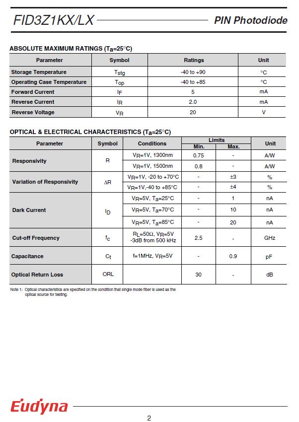
88 73
Physics of Waveguide Photodetectors with Integrated Amplification
 Physics of Waveguide Photodetectors with Integrated Amplification J. Piprek, D. Lasaosa, D. Pasquariello, and J. E. Bowers Electrical and Computer Engineering Department University of California, Santa
Introduction Fundamentals of laser Types of lasers Semiconductor lasers
 ECE 5368 Introduction Fundamentals of laser Types of lasers Semiconductor lasers Introduction Fundamentals of laser Types of lasers Semiconductor lasers How many types of lasers? Many many depending on
Optodevice Data Book ODE I. Rev.9 Mar Opnext Japan, Inc.
 Optodevice Data Book ODE-408-001I Rev.9 Mar. 2003 Opnext Japan, Inc. Section 1 Operating Principles 1.1 Operating Principles of Laser Diodes (LDs) and Infrared Emitting Diodes (IREDs) 1.1.1 Emitting Principles
Review of Semiconductor Physics
 Review of Semiconductor Physics k B 1.38 u 10 23 JK -1 a) Energy level diagrams showing the excitation of an electron from the valence band to the conduction band. The resultant free electron can freely
Lecture 18: Photodetectors
 Lecture 18: Photodetectors Contents 1 Introduction 1 2 Photodetector principle 2 3 Photoconductor 4 4 Photodiodes 6 4.1 Heterojunction photodiode.................... 8 4.2 Metal-semiconductor photodiode................
InP-based Waveguide Photodetector with Integrated Photon Multiplication
 InP-based Waveguide Photodetector with Integrated Photon Multiplication D.Pasquariello,J.Piprek,D.Lasaosa,andJ.E.Bowers Electrical and Computer Engineering Department University of California, Santa Barbara,
HIGH-EFFICIENCY MQW ELECTROABSORPTION MODULATORS
 HIGH-EFFICIENCY MQW ELECTROABSORPTION MODULATORS J. Piprek, Y.-J. Chiu, S.-Z. Zhang (1), J. E. Bowers, C. Prott (2), and H. Hillmer (2) University of California, ECE Department, Santa Barbara, CA 93106
Luminous Equivalent of Radiation
 Intensity vs λ Luminous Equivalent of Radiation When the spectral power (p(λ) for GaP-ZnO diode has a peak at 0.69µm) is combined with the eye-sensitivity curve a peak response at 0.65µm is obtained with
Quantum-Well Semiconductor Saturable Absorber Mirror
 Chapter 3 Quantum-Well Semiconductor Saturable Absorber Mirror The shallow modulation depth of quantum-dot saturable absorber is unfavorable to increasing pulse energy and peak power of Q-switched laser.
Bistability in Bipolar Cascade VCSELs
 Bistability in Bipolar Cascade VCSELs Thomas Knödl Measurement results on the formation of bistability loops in the light versus current and current versus voltage characteristics of two-stage bipolar
Vertical External Cavity Surface Emitting Laser
 Chapter 4 Optical-pumped Vertical External Cavity Surface Emitting Laser The booming laser techniques named VECSEL combine the flexibility of semiconductor band structure and advantages of solid-state
White Paper Laser Sources For Optical Transceivers. Giacomo Losio ProLabs Head of Technology
 White Paper Laser Sources For Optical Transceivers Giacomo Losio ProLabs Head of Technology September 2014 Laser Sources For Optical Transceivers Optical transceivers use different semiconductor laser
Semiconductor Lasers Semiconductors were originally pumped by lasers or e-beams First diode types developed in 1962: Create a pn junction in
 Semiconductor Lasers Semiconductors were originally pumped by lasers or e-beams First diode types developed in 1962: Create a pn junction in semiconductor material Pumped now with high current density
Robert G. Hunsperger. Integrated Optics. Theory and Technology. Sixth Edition. 4ü Spri rineer g<
 Robert G. Hunsperger Integrated Optics Theory and Technology Sixth Edition 4ü Spri rineer g< 1 Introduction 1 1.1 Advantages of Integrated Optics 2 1.1.1 Comparison of Optical Fibers with Other Interconnectors
Optoelectronic Oscillator Topologies based on Resonant Tunneling Diode Fiber Optic Links
 Optoelectronic Oscillator Topologies based on Resonant Tunneling Diode Fiber Optic Links Bruno Romeira* a, José M. L Figueiredo a, Kris Seunarine b, Charles N. Ironside b, a Department of Physics, CEOT,
Semiconductor Optical Communication Components and Devices Lecture 39: Optical Modulators
 Semiconductor Optical Communication Components and Devices Lecture 39: Optical Modulators Prof. Utpal Das Professor, Department of Electrical Engineering, Laser Technology Program, Indian Institute of
Semiconductor Optical Communication Components and Devices Lecture 18: Introduction to Diode Lasers - I
 Semiconductor Optical Communication Components and Devices Lecture 18: Introduction to Diode Lasers - I Prof. Utpal Das Professor, Department of lectrical ngineering, Laser Technology Program, Indian Institute
InP-based Waveguide Photodetector with Integrated Photon Multiplication
 InP-based Waveguide Photodetector with Integrated Photon Multiplication D.Pasquariello,J.Piprek,D.Lasaosa,andJ.E.Bowers Electrical and Computer Engineering Department University of California, Santa Barbara,
Basic concepts. Optical Sources (b) Optical Sources (a) Requirements for light sources (b) Requirements for light sources (a)
 Optical Sources (a) Requirements for light sources (b) Requirements for light sources (a)") Optical Sources (a) Optical Sources (b) The main light sources used with fibre optic systems are: Light-emitting diodes (LEDs) Semiconductor lasers (diode lasers) Fibre laser and other compact solid-state
Optical Sources (a) Optical Sources (b) The main light sources used with fibre optic systems are: Light-emitting diodes (LEDs) Semiconductor lasers (diode lasers) Fibre laser and other compact solid-state
Mode analysis of Oxide-Confined VCSELs using near-far field approaches
 Annual report 998, Dept. of Optoelectronics, University of Ulm Mode analysis of Oxide-Confined VCSELs using near-far field approaches Safwat William Zaki Mahmoud We analyze the transverse mode structure
Semiconductor Lasers Semiconductors were originally pumped by lasers or e-beams First diode types developed in 1962: Create a pn junction in
 Semiconductor Lasers Semiconductors were originally pumped by lasers or e-beams First diode types developed in 1962: Create a pn junction in semiconductor material Pumped now with high current density
Examination Optoelectronic Communication Technology. April 11, Name: Student ID number: OCT1 1: OCT 2: OCT 3: OCT 4: Total: Grade:
 Examination Optoelectronic Communication Technology April, 26 Name: Student ID number: OCT : OCT 2: OCT 3: OCT 4: Total: Grade: Declaration of Consent I hereby agree to have my exam results published on
High Bandwidth Constant Current Modulation Circuit for Carrier Lifetime Measurements in Semiconductor Lasers
 University of Wyoming Wyoming Scholars Repository Electrical and Computer Engineering Faculty Publications Electrical and Computer Engineering 2-23-2012 High Bandwidth Constant Current Modulation Circuit
LAB V. LIGHT EMITTING DIODES
 LAB V. LIGHT EMITTING DIODES 1. OBJECTIVE In this lab you are to measure I-V characteristics of Infrared (IR), Red and Blue light emitting diodes (LEDs). The emission intensity as a function of the diode
Lecture 6 Fiber Optical Communication Lecture 6, Slide 1
 Lecture 6 Optical transmitters Photon processes in light matter interaction Lasers Lasing conditions The rate equations CW operation Modulation response Noise Light emitting diodes (LED) Power Modulation
Figure Responsivity (A/W) Figure E E-09.
 Figure E E-09.") OSI Optoelectronics, is a leading manufacturer of fiber optic components for communication systems. The products offer range for Silicon, GaAs and InGaAs to full turnkey solutions. Photodiodes are semiconductor
OSI Optoelectronics, is a leading manufacturer of fiber optic components for communication systems. The products offer range for Silicon, GaAs and InGaAs to full turnkey solutions. Photodiodes are semiconductor
NON-AMPLIFIED PHOTODETECTOR USER S GUIDE
 NON-AMPLIFIED PHOTODETECTOR USER S GUIDE Thank you for purchasing your Non-amplified Photodetector. This user s guide will help answer any questions you may have regarding the safe use and optimal operation
Optoelectronic integrated circuits incorporating negative differential resistance devices
 Optoelectronic integrated circuits incorporating negative differential resistance devices José Figueiredo Centro de Electrónica, Optoelectrónica e Telecomunicações Departamento de Física da Faculdade de
THE TREND toward implementing systems with low
 724 IEEE JOURNAL OF SOLID-STATE CIRCUITS, VOL. 30, NO. 7, JULY 1995 Design of a 100-MHz 10-mW 3-V Sample-and-Hold Amplifier in Digital Bipolar Technology Behzad Razavi, Member, IEEE Abstract This paper
Resonant tunneling diode optoelectronic integrated circuits
 Invited Paper Resonant tunneling diode optoelectronic integrated circuits C. N. Ironside a, J. M. L. Figueiredo b, B. Romeira b,t. J. Slight a, L. Wang a and E. Wasige a, a Department of Electronics and
SUPPLEMENTARY INFORMATION
 SUPPLEMENTARY INFORMATION doi:10.1038/nature10864 1. Supplementary Methods The three QW samples on which data are reported in the Letter (15 nm) 19 and supplementary materials (18 and 22 nm) 23 were grown
High-efficiency, high-speed VCSELs with deep oxidation layers
 Manuscript for Review High-efficiency, high-speed VCSELs with deep oxidation layers Journal: Manuscript ID: Manuscript Type: Date Submitted by the Author: Complete List of Authors: Keywords: Electronics
CONTENTS. 2.2 Schrodinger's Wave Equation 31. PART I Semiconductor Material Properties. 2.3 Applications of Schrodinger's Wave Equation 34
 CONTENTS Preface x Prologue Semiconductors and the Integrated Circuit xvii PART I Semiconductor Material Properties CHAPTER 1 The Crystal Structure of Solids 1 1.0 Preview 1 1.1 Semiconductor Materials
Modulation of light. Direct modulation of sources Electro-absorption (EA) modulators
 modulators") Modulation of light Direct modulation of sources Electro-absorption (EA) modulators Why Modulation A communication link is established by transmission of information reliably Optical modulation is embedding
Modulation of light Direct modulation of sources Electro-absorption (EA) modulators Why Modulation A communication link is established by transmission of information reliably Optical modulation is embedding
Optical MEMS in Compound Semiconductors Advanced Engineering Materials, Cal Poly, SLO November 16, 2007
 Optical MEMS in Compound Semiconductors Advanced Engineering Materials, Cal Poly, SLO November 16, 2007 Outline Brief Motivation Optical Processes in Semiconductors Reflectors and Optical Cavities Diode
Design of InGaAs/InP 1.55μm vertical cavity surface emitting lasers (VCSEL)
") Design of InGaAs/InP 1.55μm vertical cavity surface emitting lasers (VCSEL) J.-M. Lamy, S. Boyer-Richard, C. Levallois, C. Paranthoën, H. Folliot, N. Chevalier, A. Le Corre, S. Loualiche UMR FOTON 6082
Design of InGaAs/InP 1.55μm vertical cavity surface emitting lasers (VCSEL) J.-M. Lamy, S. Boyer-Richard, C. Levallois, C. Paranthoën, H. Folliot, N. Chevalier, A. Le Corre, S. Loualiche UMR FOTON 6082
Table of Contents. Abbrevation Glossary... xvii
 Table of Contents Preface... xiii Abbrevation Glossary... xvii Chapter 1 General Points... 1 1.1. Microwave photonic links... 1 1.2. Link description... 4 1.3. Signal to transmit... 5 1.3.1. Microwave
Wavelength switching using multicavity semiconductor laser diodes
 Wavelength switching using multicavity semiconductor laser diodes A. P. Kanjamala and A. F. J. Levi Department of Electrical Engineering University of Southern California Los Angeles, California 989-1111
UNIT-III SOURCES AND DETECTORS. According to the shape of the band gap as a function of the momentum, semiconductors are classified as
 UNIT-III SOURCES AND DETECTORS DIRECT AND INDIRECT BAND GAP SEMICONDUCTORS: According to the shape of the band gap as a function of the momentum, semiconductors are classified as 1. Direct band gap semiconductors
LAB V. LIGHT EMITTING DIODES
 LAB V. LIGHT EMITTING DIODES 1. OBJECTIVE In this lab you will measure the I-V characteristics of Infrared (IR), Red and Blue light emitting diodes (LEDs). Using a photodetector, the emission intensity
PHYSICS OF SEMICONDUCTOR DEVICES
 PHYSICS OF SEMICONDUCTOR DEVICES PHYSICS OF SEMICONDUCTOR DEVICES by J. P. Colinge Department of Electrical and Computer Engineering University of California, Davis C. A. Colinge Department of Electrical
Spatial Investigation of Transverse Mode Turn-On Dynamics in VCSELs
 Spatial Investigation of Transverse Mode Turn-On Dynamics in VCSELs Safwat W.Z. Mahmoud Data transmission experiments with single-mode as well as multimode 85 nm VCSELs are carried out from a near-field
Implant Confined 1850nm VCSELs
 Implant Confined 1850nm VCSELs Matthew M. Dummer *, Klein Johnson, Mary Hibbs-Brenner, William K. Hogan Vixar, 2950 Xenium Ln. N. Plymouth MN 55441 ABSTRACT Vixar has recently developed VCSELs at 1850nm,
Semiconductor Devices
 Semiconductor Devices Modelling and Technology Source Electrons Gate Holes Drain Insulator Nandita DasGupta Amitava DasGupta SEMICONDUCTOR DEVICES Modelling and Technology NANDITA DASGUPTA Professor Department
Chapter 3 OPTICAL SOURCES AND DETECTORS
 Chapter 3 OPTICAL SOURCES AND DETECTORS 3. Optical sources and Detectors 3.1 Introduction: The success of light wave communications and optical fiber sensors is due to the result of two technological breakthroughs.
Optoelectronics ELEC-E3210
 Optoelectronics ELEC-E3210 Lecture 4 Spring 2016 Outline 1 Lateral confinement: index and gain guiding 2 Surface emitting lasers 3 DFB, DBR, and C3 lasers 4 Quantum well lasers 5 Mode locking P. Bhattacharya:
photolithographic techniques (1). Molybdenum electrodes (50 nm thick) are deposited by
. Molybdenum electrodes (50 nm thick) are deposited by") Supporting online material Materials and Methods Single-walled carbon nanotube (SWNT) devices are fabricated using standard photolithographic techniques (1). Molybdenum electrodes (50 nm thick) are deposited
Supporting online material Materials and Methods Single-walled carbon nanotube (SWNT) devices are fabricated using standard photolithographic techniques (1). Molybdenum electrodes (50 nm thick) are deposited
Optical Fibers p. 1 Basic Concepts p. 1 Step-Index Fibers p. 2 Graded-Index Fibers p. 4 Design and Fabrication p. 6 Silica Fibers p.
 Preface p. xiii Optical Fibers p. 1 Basic Concepts p. 1 Step-Index Fibers p. 2 Graded-Index Fibers p. 4 Design and Fabrication p. 6 Silica Fibers p. 6 Plastic Optical Fibers p. 9 Microstructure Optical
CHAPTER 1 INTRODUCTION
 1 CHAPTER 1 INTRODUCTION 1.1 OVERVIEW OF OPTICAL COMMUNICATION Optical fiber completely replaces coaxial cable and other low attenuation, free from electromagnetic interferences, comparatively less cost
14.2 Photodiodes 411
 14.2 Photodiodes 411 Maximum reverse voltage is specified for Ge and Si photodiodes and photoconductive cells. Exceeding this voltage can cause the breakdown and severe deterioration of the sensor s performance.
Advanced Optical Communications Prof. R. K. Shevgaonkar Department of Electrical Engineering Indian Institute of Technology, Bombay
 Advanced Optical Communications Prof. R. K. Shevgaonkar Department of Electrical Engineering Indian Institute of Technology, Bombay Lecture No. # 27 EDFA In the last lecture, we talked about wavelength
Figure 1. Schematic diagram of a Fabry-Perot laser.
 Figure 1. Schematic diagram of a Fabry-Perot laser. Figure 1. Shows the structure of a typical edge-emitting laser. The dimensions of the active region are 200 m m in length, 2-10 m m lateral width and
Laser Diode. Photonic Network By Dr. M H Zaidi
 Laser Diode Light emitters are a key element in any fiber optic system. This component converts the electrical signal into a corresponding light signal that can be injected into the fiber. The light emitter
Cavity QED with quantum dots in semiconductor microcavities
 Cavity QED with quantum dots in semiconductor microcavities M. T. Rakher*, S. Strauf, Y. Choi, N.G. Stolz, K.J. Hennessey, H. Kim, A. Badolato, L.A. Coldren, E.L. Hu, P.M. Petroff, D. Bouwmeester University
NON-AMPLIFIED HIGH SPEED PHOTODETECTOR USER S GUIDE
 NON-AMPLIFIED HIGH SPEED PHOTODETECTOR USER S GUIDE Thank you for purchasing your Non-amplified High Speed Photodetector. This user s guide will help answer any questions you may have regarding the safe
Photodiode: LECTURE-5
 LECTURE-5 Photodiode: Photodiode consists of an intrinsic semiconductor sandwiched between two heavily doped p-type and n-type semiconductors as shown in Fig. 3.2.2. Sufficient reverse voltage is applied
Figure Figure E E-09. Dark Current (A) 1.
 1.") OSI Optoelectronics, is a leading manufacturer of fiber optic components for communication systems. The products offer range for Silicon, GaAs and InGaAs to full turnkey solutions. Photodiodes are semiconductor
OSI Optoelectronics, is a leading manufacturer of fiber optic components for communication systems. The products offer range for Silicon, GaAs and InGaAs to full turnkey solutions. Photodiodes are semiconductor
64 Channel Flip-Chip Mounted Selectively Oxidized GaAs VCSEL Array
 64 Channel Flip-Chip Mounted Selectively Oxidized GaAs VCSEL Array 69 64 Channel Flip-Chip Mounted Selectively Oxidized GaAs VCSEL Array Roland Jäger and Christian Jung We have designed and fabricated
Semiconductor Optoelectronics Prof. M. R. Shenoy Department of Physics Indian Institute of Technology, Delhi
 Semiconductor Optoelectronics Prof. M. R. Shenoy Department of Physics Indian Institute of Technology, Delhi Lecture - 26 Semiconductor Optical Amplifier (SOA) (Refer Slide Time: 00:39) Welcome to this
EXAMINATION FOR THE DEGREE OF B.E. and M.E. Semester
 EXAMINATION FOR THE DEGREE OF B.E. and M.E. Semester 2 2009 101908 OPTICAL COMMUNICATION ENGINEERING (Elec Eng 4041) 105302 SPECIAL STUDIES IN MARINE ENGINEERING (Elec Eng 7072) Official Reading Time:
In this lecture we will begin a new topic namely the Metal-Oxide-Semiconductor Field Effect Transistor.
 Solid State Devices Dr. S. Karmalkar Department of Electronics and Communication Engineering Indian Institute of Technology, Madras Lecture - 38 MOS Field Effect Transistor In this lecture we will begin
Ph 77 ADVANCED PHYSICS LABORATORY ATOMIC AND OPTICAL PHYSICS
 Ph 77 ADVANCED PHYSICS LABORATORY ATOMIC AND OPTICAL PHYSICS Diode Laser Characteristics I. BACKGROUND Beginning in the mid 1960 s, before the development of semiconductor diode lasers, physicists mostly
Resonant Tunneling Device. Kalpesh Raval
 Resonant Tunneling Device Kalpesh Raval Outline Diode basics History of Tunnel diode RTD Characteristics & Operation Tunneling Requirements Various Heterostructures Fabrication Technique Challenges Application
A new picosecond Laser pulse generation method.
 PULSE GATING : A new picosecond Laser pulse generation method. Picosecond lasers can be found in many fields of applications from research to industry. These lasers are very common in bio-photonics, non-linear
Lecture 9 External Modulators and Detectors
 Optical Fibres and Telecommunications Lecture 9 External Modulators and Detectors Introduction Where are we? A look at some real laser diodes. External modulators Mach-Zender Electro-absorption modulators
Optical Amplifiers. Continued. Photonic Network By Dr. M H Zaidi
 Optical Amplifiers Continued EDFA Multi Stage Designs 1st Active Stage Co-pumped 2nd Active Stage Counter-pumped Input Signal Er 3+ Doped Fiber Er 3+ Doped Fiber Output Signal Optical Isolator Optical
Ultra-low voltage resonant tunnelling diode electroabsorption modulator
 Ultra-low voltage resonant tunnelling diode electroabsorption modulator, 1/10 Ultra-low voltage resonant tunnelling diode electroabsorption modulator J. M. L. FIGUEIREDO Faculdade de Ciências e Tecnologia,
VERTICAL CAVITY SURFACE EMITTING LASER
 VERTICAL CAVITY SURFACE EMITTING LASER Nandhavel International University Bremen 1/14 Outline Laser action, optical cavity (Fabry Perot, DBR and DBF) What is VCSEL? How does VCSEL work? How is it different
Optical Fiber Communication Lecture 11 Detectors
 Optical Fiber Communication Lecture 11 Detectors Warriors of the Net Detector Technologies MSM (Metal Semiconductor Metal) PIN Layer Structure Semiinsulating GaAs Contact InGaAsP p 5x10 18 Absorption InGaAs
Optical Receivers Theory and Operation
 Optical Receivers Theory and Operation Photo Detectors Optical receivers convert optical signal (light) to electrical signal (current/voltage) Hence referred O/E Converter Photodetector is the fundamental
3 General Principles of Operation of the S7500 Laser
 Application Note AN-2095 Controlling the S7500 CW Tunable Laser 1 Introduction This document explains the general principles of operation of Finisar s S7500 tunable laser. It provides a high-level description
R. J. Jones Optical Sciences OPTI 511L Fall 2017
 R. J. Jones Optical Sciences OPTI 511L Fall 2017 Semiconductor Lasers (2 weeks) Semiconductor (diode) lasers are by far the most widely used lasers today. Their small size and properties of the light output
Optical Receiver Operation With High Internal Gain of GaP and GaAsP/GaP Light-emitting diodes
 Optical Receiver Operation With High Internal Gain of GaP and GaAsP/GaP Light-emitting diodes Heinz-Christoph Neitzert *, Manuela Ferrara, Biagio DeVivo DIIIE, Università di Salerno, Via Ponte Don Melillo
Optical Communication and Networks M.N. Bandyopadhyay
 Optical Communication and Networks M.N. Bandyopadhyay Director National Institute of Technology (NIT) Calicut Delhi-110092 2014 OPTICAL COMMUNICATION AND NETWORKS M.N. Bandyopadhyay 2014 by PHI Learning
LEDs, Photodetectors and Solar Cells
 LEDs, Photodetectors and Solar Cells Chapter 7 (Parker) ELEC 424 John Peeples Why the Interest in Photons? Answer: Momentum and Radiation High electrical current density destroys minute polysilicon and
Conductance switching in Ag 2 S devices fabricated by sulphurization
 3 Conductance switching in Ag S devices fabricated by sulphurization The electrical characterization and switching properties of the α-ag S thin films fabricated by sulfurization are presented in this
CONTENTS. Chapter 1 Wave Nature of Light 19
 CONTENTS Chapter 1 Wave Nature of Light 19 1.1 Light Waves in a Homogeneous Medium 19 A. Plane Electromagnetic Wave 19 B. Maxwell's Wave Equation and Diverging Waves 22 Example 1.1.1 A diverging laser
Integrated Optoelectronic Chips for Bidirectional Optical Interconnection at Gbit/s Data Rates
 Bidirectional Optical Data Transmission 77 Integrated Optoelectronic Chips for Bidirectional Optical Interconnection at Gbit/s Data Rates Martin Stach and Alexander Kern We report on the fabrication and
Doppler-Free Spetroscopy of Rubidium
 Doppler-Free Spetroscopy of Rubidium Pranjal Vachaspati, Sabrina Pasterski MIT Department of Physics (Dated: April 17, 2013) We present a technique for spectroscopy of rubidium that eliminates doppler
Application Instruction 002. Superluminescent Light Emitting Diodes: Device Fundamentals and Reliability
 I. Introduction II. III. IV. SLED Fundamentals SLED Temperature Performance SLED and Optical Feedback V. Operation Stability, Reliability and Life VI. Summary InPhenix, Inc., 25 N. Mines Road, Livermore,
Lecture 4 Fiber Optical Communication Lecture 4, Slide 1
 Lecture 4 Optical transmitters Photon processes in light matter interaction Lasers Lasing conditions The rate equations CW operation Modulation response Noise Light emitting diodes (LED) Power Modulation
Photon Count. for Brainies.
 Page 1/12 Photon Count ounting for Brainies. 0. Preamble This document gives a general overview on InGaAs/InP, APD-based photon counting at telecom wavelengths. In common language, telecom wavelengths
MAHALAKSHMI ENGINEERING COLLEGE TIRUCHIRAPALLI
 MAHALAKSHMI ENGINEERING COLLEGE TIRUCHIRAPALLI - 621213 DEPARTMENT : ECE SUBJECT NAME : OPTICAL COMMUNICATION & NETWORKS SUBJECT CODE : EC 2402 UNIT III: SOURCES AND DETECTORS PART -A (2 Marks) 1. What
Objective Type Questions 1. Why pure semiconductors are insulators at 0 o K? 2. What is effect of temperature on barrier voltage? 3.
 Objective Type Questions 1. Why pure semiconductors are insulators at 0 o K? 2. What is effect of temperature on barrier voltage? 3. What is difference between electron and hole? 4. Why electrons have
HIGH SPEED FIBER PHOTODETECTOR USER S GUIDE
 HIGH SPEED FIBER PHOTODETECTOR USER S GUIDE Thank you for purchasing your High Speed Fiber Photodetector. This user s guide will help answer any questions you may have regarding the safe use and optimal
BJT. Bipolar Junction Transistor BJT BJT 11/6/2018. Dr. Satish Chandra, Assistant Professor, P P N College, Kanpur 1
 BJT Bipolar Junction Transistor Satish Chandra Assistant Professor Department of Physics P P N College, Kanpur www.satish0402.weebly.com The Bipolar Junction Transistor is a semiconductor device which
UNIT-4. Microwave Engineering
 UNIT-4 Microwave Engineering Microwave Solid State Devices Two problems with conventional transistors at higher frequencies are: 1. Stray capacitance and inductance. - remedy is interdigital design. 2.Transit
Coherent Receivers Principles Downconversion
 Coherent Receivers Principles Downconversion Heterodyne receivers mix signals of different frequency; if two such signals are added together, they beat against each other. The resulting signal contains
Chapter 6. FM Circuits
 Chapter 6 FM Circuits Topics Covered 6-1: Frequency Modulators 6-2: Frequency Demodulators Objectives You should be able to: Explain the operation of an FM modulators and demodulators. Compare and contrast;
Moderne Teilchendetektoren - Theorie und Praxis 2. Dr. Bernhard Ketzer Technische Universität München SS 2013
 Moderne Teilchendetektoren - Theorie und Praxis 2 Dr. Bernhard Ketzer Technische Universität München SS 2013 7 Signal Processing and Acquisition 7.1 Signals 7.2 Amplifier 7.3 Electronic Noise 7.4 Analog-to-Digital
Elements of Optical Networking
 Bruckner Elements of Optical Networking Basics and practice of optical data communication With 217 Figures, 13 Tables and 93 Exercises Translated by Patricia Joliet VIEWEG+ TEUBNER VII Content Preface
WIDEBAND ELECTROABSORPTION MODULATOR FOR MICROWAVE PHOTONICS
 AFRL-SN-RS-TR-2005-408 Final Technical Report December 2005 WIDEBAND ELECTROABSORPTION MODULATOR FOR MICROWAVE PHOTONICS University of California at San Diego APPROVED FOR PUBLIC RELEASE; DISTRIBUTION
ECE 340 Lecture 29 : LEDs and Lasers Class Outline:
 ECE 340 Lecture 29 : LEDs and Lasers Class Outline: Light Emitting Diodes Lasers Semiconductor Lasers Things you should know when you leave Key Questions What is an LED and how does it work? How does a
Review Energy Bands Carrier Density & Mobility Carrier Transport Generation and Recombination
 Review Energy Bands Carrier Density & Mobility Carrier Transport Generation and Recombination Current Transport: Diffusion, Thermionic Emission & Tunneling For Diffusion current, the depletion layer is
Non-amplified Photodetectors
 Non-amplified Photodetectors User Guide (800)697-6782 sales@eotech.com www.eotech.com Page 1 of 9 EOT NON-AMPLIFIED PHOTODETECTOR USER S GUIDE Thank you for purchasing your Non-amplified Photodetector
Key Questions. What is an LED and how does it work? How does a laser work? How does a semiconductor laser work? ECE 340 Lecture 29 : LEDs and Lasers
 Things you should know when you leave Key Questions ECE 340 Lecture 29 : LEDs and Class Outline: What is an LED and how does it How does a laser How does a semiconductor laser How do light emitting diodes
Non-amplified High Speed Photodetectors
 Non-amplified High Speed Photodetectors User Guide (800)697-6782 sales@eotech.com www.eotech.com Page 1 of 6 EOT NON-AMPLIFIED HIGH SPEED PHOTODETECTOR USER S GUIDE Thank you for purchasing your Non-amplified
Lab VIII Photodetectors ECE 476
 Lab VIII Photodetectors ECE 476 I. Purpose The electrical and optical properties of various photodetectors will be investigated. II. Background Photodiode A photodiode is a standard diode packaged so that
A continuous-wave Raman silicon laser
 A continuous-wave Raman silicon laser Haisheng Rong, Richard Jones,.. - Intel Corporation Ultrafast Terahertz nanoelectronics Lab Jae-seok Kim 1 Contents 1. Abstract 2. Background I. Raman scattering II.
Quantum Condensed Matter Physics Lecture 16
 Quantum Condensed Matter Physics Lecture 16 David Ritchie QCMP Lent/Easter 2018 http://www.sp.phy.cam.ac.uk/drp2/home 16.1 Quantum Condensed Matter Physics 1. Classical and Semi-classical models for electrons