High Efficiency USB Power Manager + Dual Buck + Boost + Buck-Boost DC/DC
|
|
|
- Ethan Henderson
- 5 years ago
- Views:
Transcription
1 DESCRIPTION DEMO CIRCUIT LTC3586EUFE 1306 QUICK START GUIDE LTC3586EUFE High Efficiency USB Power Manager + Dual Buck + Boost + Buck-Boost DC/DC Demonstration Circuit 1306 is a High Efficiency USB Power Manager plus Dual Buck plus Multi-Output Power Supply featuring the LTC The LTC3586 integrates a high efficiency USB Li-Ion battery charger with PowerPath control and four general purpose switching regulators, all in one chip. The PowerPath manager includes a synchronous switching low voltage input regulator, a full-featured battery charger and an ideal diode. Designed specifically for USB applications, the LTC3586 s low voltage switching regulator automatically limits its input current to a maximum of either 1x (for USB 100mA), 5x (for USB 500mA) or 10x for wallpowered applications (1A). The switching input stage provides power to VOUT where power sharing between the application circuit and the battery charger is managed. Unlike linear PowerPath controllers, the LTC3586 s switching input stage can use nearly all of the 0.5W or 2.5W available from the USB port with minimal power dissipation. This feature allows the LTC3586 to provide more power to the application and eases thermal issues in constrained applications. An ideal diode ensures that system power is available from the battery when the input current limit is reached or if the USB or wall supply is removed. The LTC3586 includes two 400mA buck regulators, one 1A buckboost regulator and one 800mA boost regulator for a variety of handheld applications. Design files for this circuit board are available. Call the LTC factory. L, LTC, LTM, LT, Burst Mode, are registered trademarks of Linear Technology Corporation. All other trademarks are the property of their respective owners. TABLE 1. Typical Specifications (25 C) Input Voltage Range: V CC 4.35V to 5.5V VOUT 3.4V to 4.7V, 1.5A (Max) LDO3V3 VOUT1 VOUT2 VOUT3 VOUT4 3.1V to 3.5V, 25mA (Max) Buck 1.16V to 1.26V, 400mA (Max) Buck 1.69V to 1.90V, 400mA (Max) Buck 3.13V to 3.51, 1.0A (Max) Buck-Boost 4.74V to 5.26V 800mA (Max) Boost 1
2 OPERATING PRINCIPLES The LTC3586 is a highly integrated power management IC which includes a high efficiency switch mode PowerPath controller, a battery charger, an ideal diode, an always-on LDO, two 400mA buck switching regulators, a 1A buck-boost switching regulator, and an 800mA boost switching regulator. All of the regulators can be independently controlled via ENABLE pins. Designed specifically for USB applications, the PowerPath controller incorporates a precision average input current buck switching regulator to make maximum use of the allowable USB power. Because power is conserved, the LTC3586 allows the load current on VOUT to exceed the current drawn by the USB port without exceeding the USB load specifications. QUICK START PROCEDURE Using short twisted pair leads for any power connections and with all loads and power supplies off, refer to Figure 1 for the proper measurement and equipment setup. The Battery should not be connected to the circuit until told to do so in the procedure below. When measuring the input or output voltage ripple, care must be taken to avoid a long ground lead on the oscilloscope probe. Measure the input or output voltage ripple by touching the probe tip directly across the VCC or VOUT and GND terminals. See Figure 2 for proper scope probe technique. The PowerPath switching regulator and battery charger communicate to ensure that the input current never violates the USB specifications. The ideal diode from BAT to VOUT guarantees that ample power is always available to VOUT even if there is insufficient or absent power at VBUS. An always on LDO provides a regulated 3.3V from available power at VOUT. Drawing very little quiescent current, this LDO will be on at all times and can be used to supply up to 20mA. Along with constant frequency PWM mode, the buck and the buck-boost switching regulators have a low power burst mode setting for significantly reduced quiescent current under light load conditions. 1. Jumper, PS and LOAD Settings to start: JP1 (NTC) = INT PS1 = OFF JP2 (ILIM0) = 0 PS2 = NC JP3 (ILIM1) = 0 LOAD1 = OFF JP4 (MODE) = 0 LOAD2 = OFF JP5 (EN1) = OFF LOAD3 = OFF JP6 (EN2) = OFF LOAD4 = OFF JP7 (EN3) = OFF LOAD5 = OFF JP8 (EN4) = OFF LOAD6 = OFF NC: Not Connected 2. Turn on PS1 and slowly increase voltage until the voltage at VBUS is 4.35V while monitoring input current. If input current exceeds 200mA turn off PS1 and look for shorts. 3. Turn on LOAD1 and LOAD2. Set LOAD1 on LDO3V3 to 5mA and LOAD2 on VOUT to 50mA in constant current mode. 2
3 4. Verify the DC voltage levels on LDO3V3 as ~3.3V, VOUT as ~4.5V and BAT as ~4.3V. 5. Continue to increase PS1 until the voltage at VBUS is 5.0V and verify the DC voltages on LDO3V3 as ~3.3V, VOUT as ~4.5V and BAT as ~4.3V. 6. Set LOAD1 to 25mA and increase LOAD2 while monitoring the input current. Verify the input limit current of ~100mA when VOUT drops below 3.4V. 7. A. Repeat with JP3 (ILIM1) and JP2 (ILIM0) in the 1 position. Verify the input limit current of ~500mA B. Repeat with JP3 (ILIM1) in the 0 position and JP2 (ILIM0) in the 1 position. Verify the input limit current of ~900mA 8. Set LOAD1 to 1mA and LOAD2 to 0mA then set JP3 (ILIM1) to the 1 position and JP2 (ILIM0) to the 0 position. Verify the DC voltage levels on LDO3V3 as <0.5V, VOUT as < 1.0Vand BAT as <VOUT. 9. Set JP3 (ILIM1) in the 0 position and JP2 (ILIM0) in the 1 position. 10. Set LOAD1 to 25mA and LOAD2 to 750mA while monitoring the input current. Verify the DC output voltage on LDO3V3 as 3.3V, VOUT as 4.3V and BAT as VOUT- ~0.3V. 11. Adjust LOAD2 until Iin is 500mA. Verify the DC voltage levels at NTC as ~2.5V, CLPROG as ~0.7V and PROG of <10mV. Verify that the FAULT and CHRG LEDs are off. 12. Adjust LOAD1 to 5mA and LOAD2 to 50mA. Set jumper JP5 (EN1) to ON position and adjust LOAD3 to 50mA. Verify the DC voltage level on VOUT1 as ~1.2V. 13. Increase LOAD3 to 400mA and verify the DC voltage level as 1.2V. Adjust LOAD3 to 50mA. 14. Set jumpers JP5 (EN1) to the OFF position, JP6 (EN2) to the ON position and adjust LOAD4 to 50mA. Verify the DC voltage on VOUT2 of ~1.8V. 15. Increase LOAD4 to 400mA and verify the DC voltage level on VOUT2 as ~1.8V. Adjust LOAD4 to 50mA. 16. Set jumpers JP6 (EN2) to the OFF position, JP7 (EN3) to the ON position and adjust LOAD5 to 50mA. Verify the DC voltage level VOUT3 as ~3.3V. 17. Increase LOAD5 to 750mA and verify the DC voltage level on VOUT3 as ~3.3V. Adjust LOAD5 to 50mA. 18. Set jumpers JP7 (EN3) to the OFF position, JP8 (EN4) to the ON position and adjust LOAD6 to 50mA. Verify the DC voltage level on VOUT4 as ~5.0V. 19. Increase LOAD6 to 600mA and verify the input current, the DC voltage level on VOUT4 as ~5.0V. Adjust LOAD6 to 50mA. 20. Set jumper JP8 (EN4) to the OFF position. 21. Turn on PS2 and adjust until the voltage at BAT is 3.6V. Verify the Iin from PS1 is ~ 450mA and the charging current going into PS2 is ~500mA. Verify that the CHRG LED is ON. Verify the DC voltage on VOUT is ~ 3.9V and VPROG is ~ 1.0V. 22. Adjust PS2 until the voltage at BAT is 4.3V. Verify the Iin from PS1 is ~ 65mA and charging current going into PS2 is < 10mA. Verify that the CHRG LED is OFF. Verify the DC voltage on VOUT is ~4.6V and VPROG is < 10mV. 3
4 23. Set Jumpers JP5 (EN1) = ON JP6 (EN2) = ON JP7 (EN3) = ON JP8 (EN4) = ON Verify LOAD1 is set to 5mA and LOAD2 LOAD5 are set to 50mA. Verify that LDO3V3, VOUT, VOUT1, VOUT2, VOUT3 and VOUT4 are enabled. 24. Using a jumper wire short the FAULT turret to a GND turret. Verify that LDO3V3 and VOUT are enabled and that VOUT1, VOUT2, VOUT3 and VOUT4 outputs are disabled. Remove the short. 25. Turn PS1 and PS2 off, wait 15 seconds and turn PS2 on and then turn PS1 on. Verify that LDO3V3, VOUT, VOUT1, VOUT2, VOUT3 and VOUT4 are enabled. 26. Verify PS2 is set at 4.3V. Adjust PS1 to 4.2V. Verify DC voltage levels on LDO3V3, VOUT, VOUT1, VOUT2, VOUT3 and VOUT4 are enabled. Verify the current is sourced from PS2. Set PS2 to 3.8V. 27. Set jumper JP1 (NTC) to EXT. Connect a 51K resistor between the NTC turret and a GND turret. The CHRG LED will blink slowly at a 1.5 Hz rate and verify that the charging current going into PS2 is ~0mA. 28. Set jumper JP1 (NTC) to EXT. Connect a 330K resistor between the NTC turret and a GND turret. The CHRG LED will blink slowly at a 1.5 Hz rate and verify that the charging current going into PS2 is ~0mA. 29. Set jumper JP1 to INT. 4
5 Figure 1. Proper Measurement Equipment Setup GND VIN Figure 2. Measuring Input or Output Ripple 5
6 Figure 3. Circuit Schematic 6


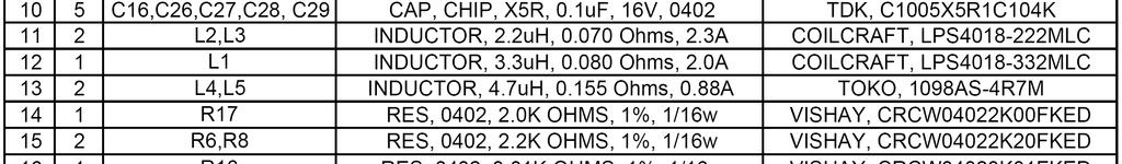

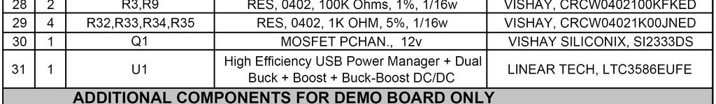
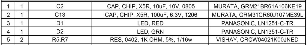

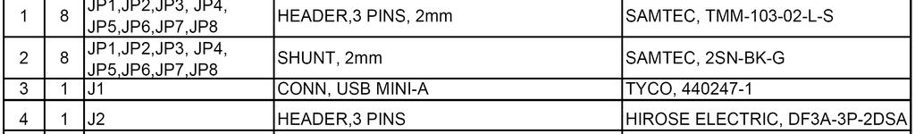
7 Figure 4. Bill of Materials 7
LTC3127EDD QUICK START GUIDE. 1A Buck-Boost DC/DC Converter with Programmable Input Current Limit DESCRIPTION
 DESCRIPTION Demonstration circuit 1451A is a Buck-Boost DC/DC converter featuring the LTC3127EDD and is ideally suited for pulsed load applications where the input current needs to be limited. Demonstration
L, LTC, LTM, LT, Burst Mode, are registered trademarks of Linear Technology Corporation. VOUT Jumper Selectable from 2.35 to 5.0V
 DEMO CIRCUIT LTC3108EDE 1582B QUICK START GUIDE LTC3108EDE/ LTC3108EDE-1 Ultralow Voltage Step-Up Converter and Power Manager DESCRIPTION Demonstration Circuit 1582B featuring the LTC3108 is a highly integrated
L, LTC, LTM, LT are registered trademarks of Linear Technology Corporation. PowerPath
 DESCRIPTION WARNING! Do not look directly at operating LED. This circuit produces light that can damage eyes. Demo Circuit 1402 is a Highly Integrated 6-Channel Portable PMIC with a push button controller,
L, LTC, Burst Mode, Bat-Track are registered trademarks of Linear Technology Corporation.
 DEMO CIRCUIT DCA Quick Start Guide : High Efficiency USB Power Manager Plus A BuckBoost Converter DESCRIPTION Demonstration Circuit A is a high efficiency USB Power/LiIon battery manager plus a A BuckBoost
L, LTC, LTM, LT are registered trademarks of Linear Technology Corporation. PowerPath
 DESCRIPTION WARNING! Do not look directly at operating LED. This circuit produces light that can damage eyes. Demo Circuit 1592A is a Highly Integrated Portable Product PMIC with a pushbutton controller,
QUICK START GUIDE. LTC3562 I 2 C Quad Synchronous Step-Down DC/DC Regulators DESCRIPTION OPERATING PRINCIPLES
 DC1123 QUICK START GUIDE DESCRIPTION Demonstration circuit 1123 is a I 2 C Quad Synchronous Step-Down DC/DC Regulators featuring the LTC3562. The LTC3562 is a quad high efficiency monolithic synchronous
QUICK START GUIDE FOR DEMONSTRATION CIRCUIT 781 HIGH EFFICIENCY SYNCHRONOUS NONISOLATED FLYBACK
 DESCRIPTION QUICK START GUIDE FOR DEMONSTRATION CIRCUIT 781 LTC3803ES6 Demonstration circuit 781 is a Telecom DC/DC converter featuring the LTC3803ES6 constant frequency current mode flyback controller.
DEMO CIRCUIT 1432A LTC3851AEUD/ QUICK LTC3851AEUD-1 SYNCHRONOUS BUCK CONVERTER DESCRIPTION QUICK START PROCEDURE
 DEMO CIRCUIT A LTC8AEUD/ QUICK LTC8AEUD- START GUIDE LTC8AEUD/ LTC8AEUD- SYNCHRONOUS BUCK CONVERTER DESCRIPTION Demonstration circuit A is a synchronous buck converter featuring the LTC8AEUD/ LTC8AEUD-.
DEMO CIRCUIT DC1303A QUICK START GUIDE LTC4098EPDC: USB Compatible Switching Power Manager/Li-Ion Charger with Overvoltage Protection DESCRIPTION
 Demonstration Circuit A is a high efficiency USB Power/LiIon battery manager plus a HV regulator battery tracking controller. The LTC98EPDC is available in a pin (mm mm.mm) UTQFN surface mount package.
DEMO CIRCUIT 928 LTC3452EUF SYNCHRONOUS BUCK-BOOST MAIN/CAMERA WHITE LED DRIVER DESCRIPTION
 DESCRIPTION WARNING! Do not look directly at operating LED. This circuit produces light that can damage eyes. Demonstration circuit 928 is a SYNCHRONOUS BUCK-BOOST MAIN/CAMERA WHITE LED DRIVER featuring
QUICK START GUIDE FOR DEMONSTRATION CIRCUIT 1231A DUAL OUTPUT, DUAL PHASE 5A SYNCHRONOUS BUCK CONVERTER
 DESCRIPTION QUICK START GUIDE FOR DEMONSTRATION CIRCUIT 1231A LTC3850EGN Demonstration circuit 1231A is a Dual Output, Dual Phase 5A Synchronous Buck Converter featuring the LTC3850EGN. The entire circuit,
TO OTHER LOADS OPTIONAL. Li-Ion. 3.3V/20mA RTC/LOW POWER LOGIC. 0.8V TO 3.6V/400mA MEMORY/ 0.8V TO 3.6V/400mA. 2.5V to 3.3V/1A I/O SYSTEM.
 Features Power Manager n High Efficiency Switching PowerPath TM Controller with Bat-Track TM Adaptive Output Control and Instant-On Operation n Programmable USB or Wall Current Limit (1mA/5mA/1A) n Full
DEMO CIRCUIT 999A QUICK START LTC3533 GUIDE LTC V, 1.5A Synchronous Buck- Boost Converter DESCRIPTION
 DEMO CIRCUIT 999A QUICK START GUIDE 3.3V, 1.5A Synchronous Buck- Boost Converter DESCRIPTION Demonstration circuit 999A is a wide input range, 3.3V, 1.5A Synchronous Buck-Boost Converterfeaturing the.
DEMO MANUAL DC2129A. LTC3119UFD 18V, 5A Synchronous Buck-Boost DC/DC Converter. Description. Performance Summary Specifications are at T A = 25 C
 Description LTC3119UFD 18V, 5A Synchronous Buck-Boost DC/DC Converter Demonstration circuit 2129A features the LTC 3119, an 18V, 5A synchronous buck/boost DC/DC converter. The DC2129A has been designed
DEMO CIRCUIT 1461A QUICK START LTC3616 GUIDE LTC A, 4MHz, MONOLITHIC SYNCHRONOUS DC/DC STEP-DOWN CONVERTER DESCRIPTION
 DESCRIPTION Demo Circuit 1461 is a high efficiency, high frequency step-down converter, incorporating the LTC3616 monolithic synchronous regulator. The DC1461A has an input voltage range of 2.25V to 5.5V,
QUICK START GUIDE FOR DEMONSTRATION CIRCUIT DC556 4A MONOLITHIC SYNCHRONOUS STEP-DOWN REGULATOR LTC3414EFE DESCRIPTION
 LTC3414EFE DESCRIPTION Demonstration circuit 556 is a high efficiency, high frequency buck converter, incorporating the LTC3414 monolithic synchronous regulator. The DC556 has an input voltage range of
LTC3566/LTC High Effi ciency USB Power Manager Plus 1A Buck-Boost Converter DESCRIPTION FEATURES APPLICATIONS TYPICAL APPLICATION
 FEATURES POWER MANAGER High Effi ciency Switching PowerPath Controller with Bat-Track Adaptive Output Control Programmable USB or Wall Input Current Limit (1mA/5mA/1A) Full Featured Li-Ion/Polymer Battery
QUICK START GUIDE FOR DEMONSTRATION CIRCUIT 968A-A ISOLATED DC/DC POWER CONVERTER LT1952 DESCRIPTION
 QUICK START GUIDE FOR DEMONSTRATION CIRCUIT 98A-A LT9 DESCRIPTION Demonstration circuit 98A-A is isolated input to high current output /8th Brick footprint converter featuring the LT 9 switching controller.
QUICK START GUIDE FOR DEMONSTRATION CIRCUIT A, 15V, MONOLITHIC SYNCHRONOUS STEP-DOWN REGULATOR
 DESCRIPTION Demonstration circuit 1215 is a step-down converter, using the LTC3605 monolithic synchronous buck regulator. The DC1215A has a maximum input voltage 15V, and is capable of delivering up to
QUICK START GUIDE FOR DEMONSTRATION CIRCUIT 1100 ISOLATED FLYBACK DC/DC CONVERTER
 DESCRIPTION QUICK START GUIDE FOR DEMONSTRATION CIRCUIT 1100 LTC3803ES6-3 Demonstration circuit 1100 is an isolated Telecom DC/DC converter featuring the LTC3803ES6-3 constant frequency current mode flyback
QUICK START GUIDE FOR DEMONSTRATION CIRCUIT 968A-B ISOLATED DC/DC POWER CONVERTER LT1952 DESCRIPTION
 LT95 DESCRIPTION Demonstration circuit 98A-B is isolated input to high current output /8th Brick footprint converter featuring the LT 95 switching controller. The DC98 converts isolated 8V to V input to
DEMO MANUAL DC1797A LTC3536 1A, Low Noise, Wide V IN Buck-Boost DC/DC Converter Description
 DEMO MANUAL DC797A LTC56 A, Low Noise, Wide V IN Buck-Boost DC/DC Converter Description Demonstration circuit 797A is a combined step-up and step-down DC/DC converter using the LTC 56 monolithic synchronous
QUICK START GUIDE FOR DEMONSTRATION CIRCUIT 968A-C ISOLATED DC/DC POWER CONVERTER LT1952 DESCRIPTION
 LT9 DESCRIPTION Demonstration circuit 98A-C is isolated input to high current output /8th Brick footprint converter featuring the LT 9 switching controller. The DC98-C converts isolated V to 7V input to
QUICK START GUIDE FOR DEMONSTRATION CIRCUIT A POLYPHASE MONOLITHIC SYNCHRONOUS BUCK REGULATOR
 DESCRIPTION Demonstration Circuit 768 is a 15A high efficiency, phase lockable constant frequency buck converter, incorporating two LTC3415 polyphase monolithic synchronous regulators. The DC768 has an
QUICK START GUIDE FOR DEMONSTRATION CIRCUIT 725 7A POLYPHASE MONOLITHIC SYNCHRONOUS BUCK REGULATOR LTC3415 DESCRIPTION
 LTC3415 DESCRIPTION Demonstration Circuit 725 is a 7A high efficiency, phase lockable constant frequency buck converter, incorporating the LTC3415 polyphase monolithic synchronous regulator. The DC725
Specifications are at T A = 25 C
 DESCRIPTION Demonstration circuit 0A is a A, bidirectional charger/ regulator featuring the LTC 6, a bidirectional synchronous step-up charger and step-down converter. DC0A implements backup by charging
QUICK START GUIDE FOR DEMONSTRATION CIRCUIT 968A-D ISOLATED DC/DC POWER CONVERTER LT1952 DESCRIPTION
 QUICK START GUIDE FOR DEMONSTRATION CIRCUIT 98A-D LT9 DESCRIPTION Demonstration circuit 98A-D is isolated input to high current output /8th Brick footprint converter featuring the LT 9 switching controller.
DEMO MANUAL DC1923A LTC V, 200mA Synchronous Buck-Boost DC/DC Converter with 1.3µA Quiescent Current
 Description DEMO MANUAL DC9A LTC9- V, 00mA Synchronous Buck-Boost DC/DC Converter with.µa Quiescent Current Demonstration circuit 9A features the LTC9-, a high efficiency 00mA buck-boost DC/DC converter
DEMO MANUAL DC1771A LTC3867EUF Synchronous Buck Converter with Remote Sensing DESCRIPTION
 LTC3867EUF Synchronous Buck Converter with Remote Sensing DESCRIPTION Demonstration circuit 1771A is a single output synchronous buck converter featuring the LTC 3867EUF with a 24-lead 4mm 4mm QFN package.
Specifications are at T A = 25 C
 LTC3245EMSE Wide V IN Range, Low Noise 250mA Buck-Boost Charge Pump Description Demonstration circuit DC1802A is a wide V IN range, low noise, 250mA buck-boost charge pump featuring the LTC 3245EMSE. Design
QUICK START GUIDE FOR DEMONSTRATION CIRCUIT 527 STEP-UP / STEP-DOWN CONVERTER WITH BURST MODE LT3433 DESCRIPTION
 DESCRIPTION QUICK START GUIDE FOR DEMONSTRATION CIRCUIT 527 LT3433 Demonstration circuit 527 is a monolithic step-up / stepdown DC/DC switching converter with Burst Mode featuring the LT3433. The board
QUICK START GUIDE FOR DEMONSTRATION CIRCUIT A, 10V, MONOLITHIC SYNCHRONOUS STEP-DOWN REGULATOR
 DESCRIPTION Demonstration circuit 1015 is a step-down converter, using the LTC3602 monolithic synchronous buck regulator. The DC1015 has an input voltage range of 4.5 to 10, and is capable of delivering
DEMO MANUAL DC1922A LTC V, 200mA Synchronous Buck-Boost DC/DC Converter with 1.3µA Quiescent Current
 Description DEMO MANUAL DC9A LTC9 5V, 00mA Synchronous Buck-Boost DC/DC Converter with.µa Quiescent Current Demonstration Circuit 9A features the LTC 9, a high efficiency 00mA buck-boost DC/DC converter
DEMO CIRCUIT 976 LT3476EUHF. Quadruple High Power LED Driver in Buck Mode DESCRIPTION. PERFORMANCE SUMMARY Specifications are at TA = 25 C
 DEMO CIRCUIT 976 QUICK START LT3476EUHF GUIDE DESCRIPTION WARNING! Do not look directly at operating LED. This circuit produces light that can damage eyes. Demonstration circuit 976 is a Quadruple High
QUICK START GUIDE FOR DEMONSTRATION CIRCUIT 1171A SYNCHRONOUS BUCK CONVERTER LTC3851EGN DESCRIPTION QUICK START PROCEDURE
 QUICK STRT GUIDE FOR DEMONSTRTION CIRCUIT 7 DESCRIPTION LTC8EGN Demonstration circuit 7 is a single output synchronous buck converter featuring the LTC8EGN. The circuit is designed with all components
DEMO MANUAL DC1964A LTC3110 2A, Bidirectional Buck-Boost DC/DC Regulator and Charger/Balancer Description
 DEMO MANUAL DC96A LTC0 A, Bidirectional Buck-Boost DC/DC Regulator and Charger/Balancer Description Demonstration circuit 96A is a A, bidirectional buckboost DC/DC regulator and charger/balancer, featuring
QUICK START GUIDE FOR DEMONSTRATION CIRCUIT 1351B SINGLE OUTPUT, HIGH POWER, HIGH EFFICIENCY POE
 DESCRIPTION LTC4269IDKD-2 Demonstration circuit 1351B is a high-power supply featuring the LTC 4269IDKD-2. This board acts as an IEEE 802.3at compliant, high power Power-over-Ethernet (PoE), Powered Device
Specifications are at T A = 25 C
 DESCRIPTION LTC65EDHC Low Noise Dual Supply with Boost and Inverting Charge Pumps Demonstration Circuit 5A has boost and inverting charge pumps each with a low noise LDO post regulator featuring the LTC
DEMO MANUAL DC2172A. LTC7138 High Efficiency, High V IN, Step-Down Regulator. Description. Performance Summary
 DEMO MANUAL DC7A Description Demonstration circuit 7A is a high input voltage, 4mA step-down regulator featuring the LTC78. The output of the regulator can be programmed for either 5V,.V or.8v with on-board
Specifi cations are at T A = 25 C. PARAMETER CONDITIONS VALUE Maximum Input Voltage
 DESCRIPTION The demo circuit 7A is a dual current mode PWM step-down DC/DC converter featuring LT 99. The demo circuit is designed for V and.v outputs from a 7V to 60V input. The current capability of
DEMO MANUAL DC1261A LTM V, 1A Step-Down µmodule Regulator DESCRIPTION
 LTM8022 36V, 1A Step-Down µmodule Regulator DESCRIPTION Demonstration circuit 1261A features the LTM 8022 stepdown μmodule regulator delivering a 3.3V output from a 4.5V to 36V input supply. As a step-down
Specifications are at T A = 25 C
 DESCRIPTION Demonstration circuit 1737A is a current-mode inverting DC/DC converter featuring the LTC 3863. The board operates from an input range of 4.5V to 16V, and provides a 5.2V, 1.7A output or a
EV2635A-R-00A Fully Power Management Charger For Single-Cell Battery System
 The Future of Analog IC Technology EV2635A-R-00A Fully Power Management Charger For Single-Cell Battery System DESCRIPTION The EV2635A-R-00A, the evaluation Board is designed to demonstrate the capabilities
Specifications are at T A = 25 C
 LT3580EDD Boost/ Inverting Regulator DESCRIPTION Demonstration circuits 1144A-A and 1144A-B feature the LT 3580EDD in Boost/Inverting Regulator configurations. The demo circuits demonstrate small size
DEMO MANUAL DC1560A LTM8048 Isolated µmodule DC/DC Converter with LDO Post Regulator DESCRIPTION BOARD PHOTO
 DESCRIPTION Demo circuit 156A is an isolated flyback μmodule DC/DC converter with LDO post regulator featuring LTM 848. The demo circuit is designed for a 6V flyback output and a 5V post regulator output
DEMO CIRCUIT 1896A LTC3633AEFE-3 DUAL CHANNEL 3A 20V MONOLITHIC SYNCHRONOUS STEP-DOWN REGULATOR DESCRIPTION QUICK START PROCEDURE
 DESCRIPTION Demonstration circuit DC896 is a dual output regulator consisting of two constant-frequency step-down converters, based on the LTC6A- monolithic dual channel synchronous buck regulator. The
LTC3610EWP DESCRIPTION
 LTC3610EWP DESCRIPTION Demonstration circuit DC119A is a synchronous step down converter featuring the LTC 3610, the high efficiency, high density DC/DC regulator. The input voltage range is from 4.5V
QUICK START GUIDE FOR DEMONSTRATION CIRCUIT 804 POWER OVER ETHERNET PD INTERFACE WITH INTEGRATED SWITCHING REGULATOR
 DESCRIPTION LTC4267 Demonstration circuit 804 is a POWER OVER ETHERNET PD INTERFACE WITH INTEGRATED SWITCHING REGULATOR featuring the LTC4267. It provides a complete IEEE 802.3af power device (PD) interface
LT3755-2, LT HIGH VOLTAGE LED CONTROLLER DESCRIPTION DEMO CIRCUIT 1268B QUICK START GUIDE
 LT3755-2, LT3755-1 HIGH VOLTAGE LED CONTROLLER DESCRIPTION Demonstration circuit 1268B-A, 1268B-B is a high voltage and high current LED driver controller. The VIN pin input voltage is as high as 40V.
Specifications are at T A = 25 C
 DESCRIPTION Demonstration circuit 258A is a 2V, 1.5A micropower synchronous step-down regulator featuring the LT 8608. The demo board is designed for 5V output from a 5.5V to 2V input. The wide input range
FEATURES n Switching Regulator with Bat-Track Adaptive. APPLICATIONS n Media Players n GPS n PDAs n Smart Phones
 FEATURES n Switching Regulator with Bat-Track Adaptive Output Control Makes Optimal Use of Limited Power Available from USB Port to Charge Battery and Power Application n Overvoltage Protection Guards
Specifications are at T A = 25 C
 DESCRIPTION Demonstration circuit 1729A is a 2.1A low dropout adjustable linear regulator featuring the LT 3086. The device is designed with multiple features and operates over a wide 1.4V to 40V input
PARAMETER CONDITION VALUE (TYPICAL) PVIN Power Input Voltage Range Operating 20V - 28V. VIN Pin Input Voltage Range Operating 8V - 14V
 PVIN Power Input Voltage Range Operating 20V - 28V. VIN Pin Input Voltage Range Operating 8V - 14V") LT3754 DESCRIPTION DC1436A is a 16-Channel High Voltage LED Driver featuring the LT3754. The LT3754 drives up to 50mA per string and has a maximum LED string voltage of 45V. DC1436A is set at 1MHz switching
LT3754 DESCRIPTION DC1436A is a 16-Channel High Voltage LED Driver featuring the LT3754. The LT3754 drives up to 50mA per string and has a maximum LED string voltage of 45V. DC1436A is set at 1MHz switching
RT9465 Evaluation Board
 3A Single Cell Li-Ion Battery Slave Switching Charger Purpose The is a switch-mode single cell li-ion/li-polymer battery charger for portable applications. It intergrates a synchronous PWM controller,
DEMO MANUAL DC961B LT1994 Low Noise, Low Distortion, Fully Differential Amplifier/Driver. Description
 Description Demonstration circuit 9 features an LT 99, low noise, low distortion, fully differential amplifier. The LT99 is a high precision, very low noise, low distortion, fully differential input/output
EV2633-R-00A Full Power Management IC For Single-Cell Battery System
 The Future of Analog IC Technology EV2633-R-00A Full Power Management IC For Single-Cell Battery System DESCRIPTION The EV2633-R-00A is the evaluation board designed to demonstrate the capabilities of
High Voltage Monolithic LED Driver DESCRIPTION
 DEMO CIRCUIT 1521A QUICK START GUIDE LT3956 LT3956 High Voltage Monolithic LED Driver DESCRIPTION Demonstration circuit 1521A is a high voltage monolithic LED driver with an integrated 3.3A, 84V power
DEMO MANUAL DC2389A. LTM V, 3A Silent Switcher μmodule Regulator. Description
 Description Demonstration circuit 2389A is a 60V, 3A step-down μmodule regulator featuring the LTM 8073. The demo board is designed for 5V output from a 7V to 60V input. The wide input range allows a variety
DEMO MANUAL DC780B Constant-Current/ Constant-Voltage 1.4MHz Step-Up DC/DC Converter DESCRIPTION
 Constant-Current/ Constant-Voltage.MHz Step-Up DC/DC Converter DESCRIPTION Demonstration circuit 780B is a Constant-Current Constant- Voltage.MHz Step-up DC/DC Converter featuring the LT 68. DC780B demonstrates
Specifications are at T A = 25 C
 Description DC184 is a dual output buck and inverting converter. It provides V and V power from 6V to 32V input. The V output can source up to 1.4 load current and the V output can source up to 800m load
Power Management. Introduction. Courtesy of Dr. Sanchez-Sinencio s Group. ECEN 489: Power Management Circuits and Systems
 Power Management Introduction Courtesy of Dr. Sanchez-Sinencio s Group 1 Today What is power management? Big players Market Types of converters Pros and cons Specifications Selection of converters 2 Motivation
QUICK START GUIDE FOR DEMONSTRATION CIRCUIT 773 SYNCHRONOUS 1MHZ LUXEON III WHITE LED DRIVER
 DESCRIPTION QUICK START GUIDE FOR DEMONSTRATION CIRCUIT 773 LTC344 & LTC050 Demonstration circuit 773 is a synchronous buck-boost MHz Luxeon III white LED driver featuring the LTC344 and LTC050. The board
MAX8969 Evaluation Kit Evaluates: MAX8969
 General Description The MAX8969 evaluation kit (EV kit) is a fully assembled and tested PCB for evaluating the MAX8969 IC. The IC is a simple 1A step-up converter in a small package that can be used in
DEMO MANUAL DC2020A LT3955EUHE 60V IN 80V OUT LED Driver. Description
 LT3955EUHE 60V IN 80V LED Driver Description Demonstration circuit 2020A is a 60V IN, 80V LED driver. It generates its own PWM waveform from its internal PWM generator for accurate PWM dimming with up
1A Buck/Boost Charge Pump LED Driver
 1A Buck/Boost Charge Pump LED Driver Description The Buck/Boost charge pump LED driver is designed for powering high brightness white LEDs for camera flash applications. The automatically switches modes
UNISONIC TECHNOLOGIES CO., LTD UB2017 Preliminary CMOS IC
 UNISONIC TECHNOLOGIES CO., LTD UB2017 Preliminary CMOS IC ONE-CELL STANDALONE LINEAR LITHIUM BATTERY CHARGER DESCRIPTION UTC UB2017 is a complete, constant current and constant voltage linear charger for
GPS+ Navigation/PDA Power Management Design
 GPS+ Navigation/PDA Power Management Design 1 GPS+Navigation/PDA System for ANPEC Solution APL5312 LDO APL5312 LDO APL5101/ APL5317 LDO VPHA_3V3 VDDPRE_1V8 VPLAD_1V2 ASIC Audio Codec APA3010/APA2010 Audio
DEMO MANUAL DC2079A LT V IN 40V OUT LED Driver. Description
 LT3954 40V IN 40V LED Driver Description Demonstration circuit 2079A is a 40V IN, 40V LED driver. It generates its own PWM waveform from its internal PWM generator for accurate PWM dimming with up to 33:1
Specifications are at T A = 25 C
 DESCRIPTION Demonstration circuit 8A is a combination step-down battery charger and step-up battery backup regulator using the LTC monolithic system power manager. The DC8A has an input voltage range from.8v
DIO6010 High-Efficiency 1.5MHz, 1A Continuous, 1.5A Peak Output Synchronous Step Down Converter
 DIO6010 High-Efficiency 1.5MHz, 1A Continuous, 1.5A Peak Output Synchronous Step Down Converter Rev 1.2 Features Low R DS(ON) for internal switches (top/bottom) 230mΩ/170mΩ, 1.0A 2.5-5.5V input voltage
DEMO MANUAL DC1453A LTM4619EV: 4.5V-28V, Dual 4A Step-Down µmodule Regulator DESCRIPTION
 DEMO MANUAL DC5A LTM69EV:.5V-8V, Dual A Step-Down µmodule Regulator DESCRIPTION Demonstration circuit 5A features the LTM 69EV, the high input voltage, high effi ciency, high density, dual A step-down
Evaluation Board for ADP2118 EVAL-ADP2118
 Evaluation Board for ADP8 EVAL-ADP8 GENERAL DESCRIPTION The evaluation (demo) board provides an easy way to evaluate the ADP8 buck regulator. This data sheet describes how to quickly set up the board to
DEMO MANUAL DC1319B-A/DC1319B-B LT3756-2/LT High Voltage LED Controller DESCRIPTION
 LT3756-2/LT3756-1 High Voltage LED Controller DESCRIPTION Demonstration circuit 1319B-A/1319B-B is a high voltage and high current LED driver controller. The V IN pin input voltage is as high as 100V,
Specifications are at T A = 25 C
 Description Demonstration circuit 0A is a V, A micropower synchronous step-down Silent Switcher with spread spectrum frequency modulation featuring the LT 860. The demo board is designed for V output from
BL8573 FEATURES DESCRIPTION APPLICATIONS TYPICAL APPLICATION. 500mA/1.5A Standalone Linear Li-Ion Battery Charge
 DESCRIPTION The is a single cell, fully integrated constant current (CC)/constant voltage (CV) Li-ion battery charger. Its compact package with minimum external components requirement makes the ideal for
FSP4054. Standalone Linear Li-ion Battery Charger with Thermal Regulation
 FEATURES Programmable charge current up to 800mA No MOSFET, sense resistor or blocking diode required Complete linear charger in thin SOT package for single cell lithium ion batteries Constant-current/constant-voltage
QUICK START GUIDE FOR DEMONSTRATION CIRCUIT 566 DIGITALLY CONTROLLED PROGRAMMABLE GAIN AMPLIFIER LTC6910 DESCRIPTION
 LTC691 DESCRIPTION Demonstration circuits 566A-A, -B and -C, feature the easy to use, rail-to-rail input and output LTC691 series of Low Noise Programmable Gain Amplifier (PGA) parts. The inverting gain
AL3157 Evaluation Module
 Device Features Dual-Mode 1x and 2x Charge Pump V IN Range: 2.7V to 5.5V Up to 300mA total drive capability: Three 30mA and One 210mA Channels Two Simple PWM Dimming Control Inputs 1.2 MHz Constant Switching
MP5090 Low I Q, Dual-Channel, 3A/2A Load Switch
 MP5090 Low I Q, Dual-Channel, 3A/2A Load Switch The Future of Analog IC Technology DESCRIPTION The MP5090 integrates dual load switches to provide load protection covering a 0.5V to 5.5V voltage range.
Extending Cell Phone Battery Life with the ISL9109
 Extending Cell Phone Battery Life with the ISL9109 Application Note AN1424.0 In this day and age practically everyone is armed with a cell phone. Some of these smart phones not only work as a cell phone
OCTOBER 2007 VOLUME XVII NUMBER 3. Low Dropout Regulator Can Be Directly Paralleled to Spread The Heat
 LEAR TECHNOLOGY OCTOBER 2007 VOLUME XVII NUMBER 3 THIS ISSUE Cover Article Low Dropout Regulator Can Be Directly Paralleled to Spread The Heat...1 Robert Dobkin Linear in the News...2 Design Features 16-Channel
Specifications are at T A = 25 C
 DESCRIPTION Demonstration circuit 23A is a 42V, 6A micropower synchronous step-down second generation Silent Switcher with spread spectrum frequency modulation featuring the LT864S. The demo board is designed
I LOAD LOAD R IN V + LT6110 IMON DC2033 F01. Figure 1. One Cable/Wire Compensation (One Wire to a Load Sharing the Regulator s Ground) LT6110
 LT6110") + Description The DC2033A demo board features the LT 6110 cable/ wire drop compensator IC. The is a precision high side current sense that monitors load current via a sense resistor and converts the sense
+ Description The DC2033A demo board features the LT 6110 cable/ wire drop compensator IC. The is a precision high side current sense that monitors load current via a sense resistor and converts the sense
PARAMETER CONDITION VALUE Minimum Input Voltage. Maximum Input Voltage. Maximum Output Current for 3.3Voutput. Maximum Output Current for 2.
 ECRIPTION QUICK TART UIE FOR EMONTRATION CIRCUIT 541A LTC3723-1, LTC3901, LT3710 and LT1431 emonstration circuit 541A is an isolated synchronous push-pull converter featuring the LTC3723-1, LTC3901, LT1431
MIC5317. Features. General Description. Applications. Typical Application. High-Performance Single 150mA LDO
 High-Performance Single 150mA LDO General Description The is a high performance 150mA low dropout regulator offering high power supply rejection (PSRR) in an ultra-small 1mm 1mm package for stringent space
Specifications are at T A = 25 C
 DEMO MANUAL DC66A LT590 48V Buck-Mode LED Driver WARNING! DO NOT LOOK DIRECTLY AT OPERATING LED This Circuit Produces Light that Can Damage Eyes. DESCRIPTION Demonstration circuit 66A is a 48V Buck-Mode
QUICK START GUIDE FOR DEMONSTRATION CIRCUIT 543 LTC2920 WITH DUAL DC TO DC CONVERTER
 DESCRIPTION QUICK START GUIDE FOR DEMONSTRATION CIRCUIT 543 LTC2920-2 Demonstration circuit 543 is an LTC 2920-2 Dual Voltage Margining Controller integrated with an LTC1628 Dual High Efficiency, 2-Phase
MIC Features. General Description. Applications. Typical Application. 1.5A, Low-Voltage µcap LDO Regulator
 1.5A, Low-Voltage µcap LDO Regulator General Description The Micrel is a 1.5A low-dropout linear voltage regulator that provides a low-voltage, high-current output with a minimum of external components.
MIC General Description. Features. Applications: Typical Application. 1A High Speed Low VIN LDO
 1A High Speed Low VIN LDO General Description The is a high speed, Low V IN LDO capable of delivering up to 1A and designed to take advantage of point of load applications that use multiple supply rails
DT V 400KHz Boost DC-DC Controller FEATURES GENERAL DESCRIPTION APPLICATIONS ORDER INFORMATION
 GENERAL DESCRIPTION The DT9150 is a 5V step-up DC/DC controller designed capable of deliver over 50V Output with proper external N-MOSFET devices. The DT9150 can work with most Power N-MOSFET devices,
DEMO MANUAL DC2247A LT V 2A Synchronous 2MHz Boost LED Driver. Description
 Description Demonstration circuit DC2247A is a 36V 2A synchronous 2 boost LED driver featuring the LT 3922. It drives a single string of LEDs at 3mA up to 34V when V IN is between 7V and 28V. It runs down
Specifications are at T A = 25 C
 DEMO MANUAL DCA Description LT871 Synchronous Four-Quadrant Converter Demonstration circuit A is a synchronous fourquadrant converter featuring the LT 871 switching controller. The LT871 can regulate to
PARAMETERS CONDITIONS VALUE
 DEMO BOARD MANUAL DC324 LTC1876 High Efficiency, Low Cost, 3-Output Power Supply DESCRIPTION Demonstration Board DC324 is a high efficiency, low cost design using the LTC 1876. This demo board provides
IS32LT3172/73 10-TO-200MA CONSTANT-CURRENT LED DRIVER
 DESCRIPTION The IS32LT3172/73 is adjustable constant current linear devices with excellent temperature stability. A single resistor is all that is required to set the operating current from 10mA to 200mA.
DIO6305 High-Efficiency 1.2MHz, 1.1A Synchronous Step-Up Converter
 High-Efficiency 1.2MHz, 1.1A Synchronous Step-Up Converter Rev 1.2 Features High-Efficiency Synchronous-Mode 2.7-5.25V input voltage range Device Quiescent Current: 30µA (TYP) Less than 1µA Shutdown Current
MP28164 High-Efficiency, Single-Inductor, Buck-Boost Converter with 4.2A Switches
 The Future of Analog IC Technology MP28164 High-Efficiency, Single-Inductor, Buck-Boost Converter with 4.2A Switches DESCRIPTION The MP28164 is a high-efficiency, lowquiescent current, buck-boost converter
0.6-3VIN, VOUT,
 FEATURES Boost Regulator Input Voltage: 0.6V- 3V Output Voltage: 3V Shutdown Control Jumper Coilcraft 10µH Inductor (LPS4018-103ML) Resistor Pad Available for Anti-Crush TM Voltage Setting COMPONENT LIST
DEMO MANUAL DC2568A LTM4622A Ultrathin Dual 2A Step-Down µmodule Regulator DESCRIPTION BOARD PHOTO
 DESCRIPTION Demonstration circuit 568A features the LTM 46A µmodule regulator, a tiny low profile high performance high efficiency dual step-down regulator. The LTM46A has an operating input voltage range
OUT to. Specifications are at T A = 25 C. PARAMETER CONDITIONS MIN TYP MAX UNITS Input Voltage V Output Voltage
 DESCRIPTION LT80 Micropower No-Opto Isolated Flyback Converter with 50V/A Switch Demonstration circuit 9A is a micropower no-opto isolated flyback converter featuring the LT 80. This demo circuit outputs
LTC4099 I 2 C Controlled USB Power Manager/Charger with Overvoltage Protection Description. Features. Applications. Typical Application
 Features n Switching Regulator with Bat-Track Adaptive Output Control Makes Optimal Use of Limited Input Power n I 2 C Port for Optimal System Performance and Status Information n Input Overvoltage Protection