CHETTINAD COLLEGE OF ENGINEERING & TECHNOLOGY NH-67, TRICHY MAIN ROAD, PULIYUR, C.F , KARUR DT.
|
|
|
- Aileen Cathleen Parsons
- 5 years ago
- Views:
Transcription
1 CHETTINAD COLLEGE OF ENGINEERING & TECHNOLOGY NH-67, TRICHY MAIN ROAD, PULIYUR, C.F , KARUR DT. DEPARTMENT OF ELECTRONICS AND COMMUNICATION ENGINEERING COURSE MATERIAL Subject Name: Analog & Digital Communication Subject Code: CS2204 Class / SEM: B. E. (CSE) / III Staff Name: Suganya. J UNIT II DIGITAL COMMUNICATION Syllabus: Introduction, Shannon limit for information capacity, digital amplitude modulation, frequency shift keying, FSK bit rate and baud, FSK transmitter, BW consideration of FSK, FSK receiver, phase shift keying binary phase shift keying QPSK, Quadrature Amplitude modulation, bandwidth efficiency, carrier recovery squaring loop, Costas loop, DPSK. DIGITAL COMMUNICATION Objectives: To study different types of digital modulation techniques like ASK, FSK and PSK, QAM and QPSK. To learn to construct FSK transmitter and Receiver. History & Development: The trend in communication is not from analog to digital but actually digital communication came first by practical means of electrical communication by using Morse code. It is a digital form of Code consisting of three elements dot, dash and space.
2 Many of the signals in modern communication are digital. For example, codes for alphanumeric characters and binary data used in computer programs. Also digital techniques can be used for analog signal transmission. Advantages of Digitizing a Signal: Improved transmission quality. Reduction in distortion. Improvement in SNR. Types of Signal Transmission: Analog signal is sent over a channel with no modulation. For e.g., the ordinary public address system consists of only microphone, amplifier, speaker and a twisted pair wire as channel. Analog Source Baseband channel Analog Destination Analog transmission is done using modulation and demodulation. It is used in radio and TV broadcasting. Analog Source Channel Modulator Demodulator Analog Destination Transmitter Receiver Digital signal is transmitted through digital channel as digital pulses. Digital Source Channel Coder Decoder Digital Destination The channel can not transmit pulses directly. For example, the radio channel requires a modulation process and an ordinary telephone connection can not pass dc. The digital
3 signal has to be modulated on to a carrier at one end and demodulated at receiver. The modem is a combination of modulator and demodulator. Channel Digital Source Analog Modem Modem Digital Destination Analog signal can be converted to digital form, transmitted and digital is converted back to analog form in receiver. Analog Source ADC & Coding Digital Decoding & DAC Analog Destination Channel The channel can not carry pulses so modulation and demodulation is required. It is used in voice transmission. Analog Source ADC & Coding Modem Analog Modem Decoding Channel & DAC Analog Destination The fastest growing area in communication is the use of digital techniques with analog signal. There is no way to remove noise and distortion from analog signals since it is added cumulative in transmitter, channel and receiver. Signal to noise ratio (SNR) decreases with increase in the distance when passed through amplifiers and channels as in long distance telephone communication system. Digital signals are not immune to noise, but decrease the effect of noise and distortion. Digital system decreases the probability of error to a very small value since it uses some techniques of error detection and correction. Distortion can be removed using regenerative repeaters. Distorted Signal Receiver Transmitter Regenerated Signal
4 Advantages of Digital Communication: Convenience in multiplexing. Mostly it is used in Time Division Multiplexing for transmitting both voice and data over same communication channel. It is most suitable for digital transmission. Convenience in switching. Disadvantages of Digital Communication: Greater Complexity. Larger transmission bandwidth. To overcome disadvantages, Large scale low cost digital ICs decreases the difficulty and expense of constructing complex circuitry. Data compression techniques with wider bandwidth media (fiber optic cable) decreases bandwidth penalty. So the advantages overweigh the disadvantages. INTRODUCTION: Electronic Communication refers to transmission, reception and processing of information using electronic circuits. Information is the knowledge or intelligence communicated between two or more data points. Digital Modulation is the transmission of digitally modulated analog signal (carrier) between two or more points in a communication system. It is also called as digital radio system since digitally modulated signals can be propagated through earth s atmosphere which is used in wireless communication system. Traditional analog systems like AM, FM and PM are replaced by modern digital modulation systems. Advantages of Digital Modulation System: Ease of processing. Ease of multiplexing. High noise immunity.
5 Digital Communication includes systems where relatively high frequency analog carriers are modulated by relatively low frequency digital information signals. It is used in digital radio systems. Digital Transmission Systems transport information in digital form and it requires a physical facility between transmitter and receiver. The physical medium can be a metallic wire pair, coaxial cable, optical fiber cable. Digital radio system uses a physical cable or free space as a communication channel. Analog and digital modulation communication system differs in the nature of the modulating signal. Both analog and digital modulation system uses analog carriers to transport information through the channel. In analog modulation, both the information and carrier are analog. In digital modulation, the information is digital (computer generated data or digitally encoded analog signal) and the carrier is analog. The digital modulation system is mathematically represented as (3.1) If the information is digital and the amplitude (V) of the carrier is varied proportional to the digital information signal, a digitally modulated signal called Amplitude Shift Keying (ASK) is produced. If the information is digital and the frequency (f) of the carrier is varied proportional to the digital information signal, a digitally modulated signal called Frequency Shift Keying (FSK) is produced. If the information is digital and the phase (θ) of the carrier is varied proportional to the digital information signal, a digitally modulated signal called Phase Shift Keying (PSK) is produced.
6 Quadrature Amplitude Modulation (QAM) results if both the amplitude and the phase are varied proportional to the digital information signal. ASK, FSK, PSK and QAM are all forms of digital modulation. Advantages of digital modulation: It is suited to a multitude of communication applications including both cable and wireless communication. Noise immunity is high. Several error detection and correction methods are available. Applications of digital modulation: It is used in relatively low speed voice band data communication modems in most personal computers. It is used in relatively high speed data transmission systems such as broadband digital subscriber lines (DSL). It is also used in digital microwave and satellite communication systems. It is widely used in cellular telephone personal communication systems (PCS). Digital Modulation System: Figure 3.1 shows the simplified block diagram of digital modulation system or digital radio system.
7 Precoder performs the level conversion. It encodes the incoming data into a group of bits that modulated an analog carrier. The modulated carrier is shaped (filtered), amplified and then transmitted through the transmission medium to the receiver. The transmission medium may be a metallic wire, optical fiber cable, earth s atmosphere or a combination of two or more types of transmission systems. In receiver, the incoming signals are filtered, amplified and then applied to the demodulator and decoder circuits which extract the original source information from the modulated carrier. The clock and carrier recovery circuits recover the analog carrier and digital timing clock signals from the incoming modulated wave since they are necessary to perform demodulation process. Shannon Limit for Information Capacity: Information theory is highly theoretical study of efficient use of bandwidth to propagate information through electronic communication systems. It is used to determine the information capacity of a data communication system. Information Capacity is a measure of how much information can be propagated through a communication system. It is a function of bandwidth and transmission time. It represents the number of independent symbols that can be carried through a system in a given unit of time. The most basic digital symbol used to represent information is binary digit or Bit. It is convenient to express the information capacity of a system as a Bit Rate. Bit Rate is the number of bits transmitted during one second and is expressed in bits per second (bps). The useful relationship among bandwidth, transmission time and information capacity was given by R. Hartley of Bell Telephone Laboratories in Hartley s Law is given by,
8 (3.2) The information capacity is a linear function of bandwidth and transmission time and is directly proportional to both. Either the bandwidth or the transmission time changes, a directly proportional change occurs in information capacity also. Shannon in 1948 related the information capacity of a communication channel to bandwidth and signal to noise ratio (SNR). SNR is the ratio of signal power to noise power and is unit less. SNR in db is calculated as 10 log 10 (SNR) db. Increase in SNR provides better performance and higher the information capacity since SNR is directly proportional to the signal power. Shannon Limit for Information Capacity is (3.3) Problem.1: For a standard telephone circuit with SNR of 30 db and a bandwidth of 2.7 KHz, determine the Shannon limit for information capacity. Given, 10 Log 10 SNR = 30 db SNR = 10 3 = 1000 B = 2.7 KHz Then,
9 I = 3.32 B Log 10 (1+SNR) = 3.32 x 2.7 x 10 3 Log 10 (1+1000) = 26.9 Kbps. Conclusion: 26.9 kbps information can be transmitted through a 2.7 KHz communication channel. This is true but can not be done with a binary system. To achieve information rate of 26.9 kbps through a 2.7 KHz channel, each symbol transmitted must contain more than one bit. M-ary Encoding: M-ary is derived from the word binary. Here M represents a digit that corresponds to the number of conditions, levels or combinations possible for a given number of binary variables. It is advantageous to use a level higher than binary which is called as beyond binary or higher than binary encoding. For example, digital signal with 4 possible conditions like voltage levels, frequency, phase and time is represented as a system with M=4. The number of bits necessary to produce a given number of conditions is expressed mathematically as (3.4) If N = 1, M = 2 N = 2; If N= 2, M=4; If N=3, M=8 and so on. Bit Rate is the rate of change of a digital information signal usually binary. Baud is the rate of change of a signal on the transmission medium after encoding and modulation have occurred. Its unit is symbols/second.
10 Baud is a unit of transmission rate or modulation rate or symbol rate. It is also defined as the reciprocal of one output signaling element which represents several number of bits. (3.5) Signaling element is a symbol encoded as a change in amplitude, phase or frequency. Baud contains more than one information bit. Baud = Bit Rate in BFSK and BPSK systems. Baud < Bit Rate in QPSK and 8 PSK systems. Nyquist states that The binary digital signal can be propagated through an ideal noiseless transmission medium at a rate equal to two times the bandwidth of the medium. The minimum theoretical bandwidth necessary to propagate a signal is called Minimum Nyquist Bandwidth or Minimum Nyquist Frequency. (3.6) Actual bandwidth depends on the type of encoding, modulation used, type of filters used, system noise and desired error performance. Ideal bandwidth is used for comparison purposes only. For a given bandwidth B, highest theoretical bit rate is 2B. For example, a standard telephone circuit has B = 2700 Hz has a capacity of 5400 bps to propagate through it. If there is more than one level for signaling, then more than one bit is transmitted at a time and so it is possible to propagate a bit rate that exceeds 2B.
11 The Nyquist formulation for information capacity using multilevel signaling is given by (3.7) The minimum bandwidth necessary to pass M-ary digitally modulated carriers is (3.8) The information bits are encoded (grouped) and converted to signal with more than two levels. Then the transmission rate in excess of 2B is possible. Therefore, the BAUD is the encoded rate of change and is also equals to the bit rate divided by the number of bits encoded into one signaling element. (3.9) Baud and ideal minimum Nyquist bandwidth have the same value and is equal to the bit rate divided by the number of bits necessary to encode. This is true for all forms of digital modulation. Digital Modulation Techniques: The digital modulation techniques are classified into two types; Coherent Techniques and Non-coherent Techniques. In Coherent Technique, the receiver is equipped with a phase recovery circuit. In Non-coherent technique, there is no phase recovery circuit in the receiver. Phase recovery circuit ensures the oscillator supplying the locally generated carrier wave in the receiver is synchronized in both phase and frequency to the oscillator
12 supplying the carrier wave used to originally modulate the incoming data stream in the transmitter. In pass band data transmission, signals are generated by changing the amplitude, phase or frequency of a sinusoidal carrier in M discrete steps. The different methods of modulation are combined into a hybrid form to generate M- ary signal. For example, discrete changes in both amplitude and phase of a carrier combined to produce M-ary Amplitude Phase Shift Keying (APK). M-ary ASK is a special case of M-ary QAM. M-ary signaling is mostly used since it conserves bandwidth at the expense of increased power. Digital Amplitude Modulation (DAM): This is the simplest digital modulation technique also called as Amplitude Shift Keying (ASK). Here a binary information signal directly modulates the amplitude of an analog carrier. This is similar to standard AM except that only two output amplitudes are possible. This is also called as Digital Amplitude Modulation for this reason. Mathematically this is expressed as, (3.10) The modulating signal v m (t) is a normalized binary waveform where +1 V for logic 1 and -1 V for logic 0. For a logic 1 input, v m (t) = +1 V, (3.11)
13 For a logic 0 input, v m (t) = -1 V, (3.12) The modulated wave v ask (t) is either A Cos (ω C t) or 0. Therefore, the carrier is either ON or OFF. So the ASK is also referred as ON-OFF Keying (OOK). Figure 3.2 shows the input and output waveforms of ASK modulator. For every change in the input binary data stream, there is one change in the ASK waveform and the time of one bit (t b ) equals the time of one analog signaling element (t S ). For the entire time the binary input is high, the output is a constant amplitude constant frequency sinusoidal wave. For the entire time the binary input is low, the carrier is OFF. (3.13) (3.14) The rate of ASK waveform (baud) is same as the rate of change of binary input in bps. Therefore, bit rate = baud. With ASK, bit rate = minimum Nyquist bandwidth.
14 Therefore For ASK, N=1. (3.15) Advantages of ASK: It is a low cost type of digital modulation technique. It is seldom used except for very low speed telemetry circuits. Disadvantages of ASK: It is a low quality system. It is susceptible to noise. Amplitude non-linearities are produced in microwave radio and satellite communication channels. It is not suitable for pass band data transmission over non-linear channels. Applications of ASK: The telephone and cable system used ASK previously but not used nowadays due to its non-linearities and susceptibility to noise. Frequency Shift Keying (FSK): FSK is a relatively simple low performance type of digital modulation. It is a form of constant amplitude angle modulation similar to standard FM except the modulating signal is a binary signal that varies between two discrete voltage levels rather than a continuously changing analog waveform It is also called as Binary FSK (BFSK). The general expression for BFSK signal is,
15 The phase shift in carrier frequency ( f) is directly proportional to the amplitude of the binary input signal v m (t). The direction of the shift is determined by the polarity. The modulating signal is a normalized binary waveform where a logic 1 = +1 V and a logic 0 = -1 V. For a logic 1 input, v m (t) = +1, For a logic 0 input, v m (t) = -1, With binary FSK, the center carrier frequency (f C ) is shifted (deviated) up and down in frequency domain by the binary input signal.
16 As the binary input signal changes from a logic 0 to logic 1 and vice versa, the output frequency shifts between two frequencies (a mark or logic 1 frequency (f m ) and a space or logic 0 frequency (f S )). The mark and space frequencies are separated from the carrier frequency by peak frequency deviation ( f) and from each other by 2 f. The frequency deviation is the difference between either mark or space frequency and center frequency or half the difference between mark and space frequency. Figure 3.4 shows the binary input to FSK modulator and corresponding FSK output.
17 When the binary input (f b ) changes from logic 1 to logic 0 and vice versa, the FSK output frequency shifts from a mark frequency (f m ) to a space frequency (f S ) and vice versa. The mark frequency is the higher frequency (f C + f) and the space frequency is the lower frequency (f C - f). The truth table for binary FSK modulator shows the input and output possibilities for a given digital modulation scheme FSK Bit Rate, Baud and Bandwidth: The time of one bit (t b ) is same as the time the FSK output is a mark or space frequency (t S ). The bit time is equal to the time of FSK signaling element. Therefore, the bit rate is equal to baud. For N=1, Baud = (f b /N) = f b. FSK is exception to the rule for digital modulation as minimum bandwidth is not determined from B = (f b /N). The minimum bandwidth for FSK is,
18 Equation (3.21) resembles the Carson s rule for determining the approximate bandwidth for an FM wave. The difference is, for FSK, the bit rate (f b ) is substituted for the modulating signal frequency (f m ). Bessel function can also be used to determine approximate bandwidth for FSK wave. Time of one bit, t b = (1/f b ). where f m is the mark frequency. f s is the space frequency. T 1 is the period of shortest cycle. (1/T 1 ) is the fundamental frequency of the binary square wave. f b is the input bit rate in bps. The fastest rate of change (highest fundamental frequency) in a NRZ binary signal occurs when alternating 0 s and 1 s are occurring. (i.e., a square wave). Since it takes a high and a low to produce a cycle, the highest fundamental frequency present in a square wave is equal to the repetition rate of the square wave. For example, with binary signal, it is equal to half the bit rate [i.e. = (f b /2)].
19 where f a is the fundamental frequency of the binary input signal in Hertz. f b is the input bit rate in bps. The formula used for modulation index in FM is valid for FSK. Therefore, f h = (unit less) f a where h is the h-factor in FSK, same as modulation index in FM. f a is the fundament The worst case modulation index (deviation ratio) is that which yields widest bandwidth. The worst case/widest bandwidth occurs when both the frequency deviation and modulating signal frequency are at their maximum values. The peak frequency deviation in FSK is constant and always at its maximum value. The highest fundamental frequency is equal to half the incoming bit rate. where h is the h-factor (unit less). f m is the mark frequency in Hertz. f S is the space frequency in Hertz. f b is the bit rate in bps. Problem: 1. Determine the a) peak frequency deviation b) minimum bandwidth and c) baud for a BFSK signal with a mark frequency of 49 KHz, space frequency of 51 KHz and an input bit rate of 2 kbps. 2. Using Bessel Table, determine the minimum bandwidth for the same FSK signal given in problem 1, above.
20 FSK Transmitter: Figure 3.6 shows a simplified binary FSK modulator. It is very similar to conventional FM modulator and is very often a Voltage Controlled Oscillator (VCO) since the voltage is made constant and only the frequency is varying. The center frequency (f c ) is chosen such that it falls half way between the mark and space frequency. A logic 1 input shifts the VCO output to the mark frequency and a logic 0 input shifts the VCO output to the space frequency. As the binary input changes back and forth between logic 1 and logic 0 conditions, the VCO output also shifts or deviates back and forth between mark and space frequencies. IN BFSK modulator, f is the peak frequency deviation of the carrier and is equal to the difference between the carrier rest frequency and either the mark or space frequency (or half the difference between mark and space frequencies). A VCO FSK modulator can be operated in sweep mode where peak frequency deviation is simply the product of binary input voltage and the deviation sensitivity of VCO. With sweep mode of modulation, frequency deviation is expressed mathematically as f = K 1 V m (t) (3.24) where f is the peak frequency deviation in Hz. V m (t) is the peak binary modulating signal voltage in volts. K 1 is the deviation sensitivity in Hz/Volt.
21 With BFSK, the amplitude of the input signal can only be one of the two values, one for logic 1 and the other for logic 0 conditions. Therefore the peak frequency deviation is constant and is always at its maximum value. The frequency deviation is simply plus or minus the peak voltage of the binary signal times the deviation sensitivity of the VCO. Since the peak voltage is same for a logic 1 as it is for logic 0, the magnitude of frequency deviation is also the same for logic 1 as it is for logic 0. FSK Receiver: FSK demodulation is quite simple as shown in Figure 3.7. The FSK input signal is simultaneously applied to the inputs of both band pass filters (BPF) through a power splitter. The respective filter passes only the mark or only the space frequency on to its respective envelope detector. Envelope detectors indicate the total power in each pass band and the comparator responds to the largest of the two powers. This type of FSK detection is referred as non-coherent detection since there is no frequency involved in the demodulation process that is synchronized either in phase, frequency or both with the incoming signal.
22 The incoming FSK signal is multiplied by a recovered carrier signal that has the exact same frequency and phase as the transmitter reference. The two transmitted frequencies (mark and space frequencies) are not generally continuous; so it is not practical to produce a local reference that is coherent with both of them. The coherent FSK detection is seldom used. The most common circuit used for demodulating BFSK signal is PLL-FSK detector. It works similar to PLL-FM demodulator. As the input to PLL shifts between the mark and space frequencies, the dc error voltage at the output of phase comparator follows the frequency shift. Since only two input frequencies are used, there are also only two output error voltages. One represents logic 1 and the other represents logic 0. Therefore, the output is a two-level (binary) representation of FSK input.
23 Generally the natural frequency of the PLL is equal to the center frequency of FSK demodulator. The changes in the dc error voltage follow the changes in the analog input frequency and are symmetrical around 0V. Figure 3.10 Input and Output Waveforms of PLL FSK Demodulator Advantages of FSK: Since FSK is a robust scheme, it is used in telegraphy systems. It is reliable in the presence of noise. It is possible to use more than two frequencies to increase the symbol rate. Disadvantages of FSK: BFSK is not efficient in terms of bandwidth since each symbol has only two possible states. High frequency radio channel tend to be very noisy and phase shifts are introduced into the signal when it is traveled through the ionosphere. So, it is impractical to maintain accurate phase information. It provides only low data rate for high frequency communication.
24 Applications of FSK: FSK is used for low data rate applications such as pagers. It is used for transmitting burst of data over systems that are mainly analog. It is used extensively in high frequency radio systems for radio teletype transmission. It is used in VHF Amateur radio link. Gaussian minimum shift keying (GMSK) which is a special case of FSK is used in Global system for mobile communication (GSM) cellular radio and Personal Communication System (PCS). It is also used in telephone transmission system. Continuous Phase FSK: The continuous-phase FSK is a binary FSK where the mark and space frequencies are synchronized with the binary input bit rate. Synchronous implies that there is a precise time relationship between two frequencies; it does not mean both are equal. The mark and space frequencies are selected in such a way that they are separated from the center frequency by an exact multiple of one half the bit rate [f m = f s = n (f b /2) where n is any integer]. It provides a smooth phase transition in analog output signal when it changes from f s to f m and vice versa. It avoids phase discontinuity between f s and f m when the binary input changes from logic 0 to logic 1. Advantage: It provides better error performance than conventional BFSK for a given SNR. Disadvantage: It requires synchronization circuits and is more expensive to implement.
25 Phase Shift Keying (PSK): Phase Shift Keying is also another form of angle modulated, constant amplitude digital modulation. It is an M-ary digital modulation scheme similar to conventional Phase Modulation except with PSK, the input is a binary digital signal and limited numbers of output phases are possible. The input binary information is encoded into groups of bits before modulating the carrier. The number of output phases is defined by M = 2 N and determined by the number of bits (N) in the group. Binary Phase Shift Keying (BPSK): BPSK is the simplest form of Phase shift keying where N = 1 and M = 2 N = 2. With BPSK, two phases are possible for carrier, one phase represents logic 1 and the other phase represents a logic 0. As the input digital signal changes the state from logic 1 to logic 0 or logic 0 to logic 1, the phase of the output carrier shifts between the two angles separated by 180. It is also called as Phase Reversal Keying (PRK) or Biphase modulation. BPSK is a form of square wave modulation of a continuous wave signal. BPSK Transmitter: Figure 3.11 shows the simplified block diagram of a BPSK Transmitter. Here the balanced modulator acts as a phase reversing switch. Since bipolar signals are more power efficient to encode binary data with voltages equal in magnitude but opposite in polarity and symmetrically balanced about 0V. Assume 1Ω resistance and logic 1 level of +5V and a logic 0 level of 0V required an average power of 12.5W, assuming equal probability of occurrence for logic 0 and logic 1. With logic 1 of +2.5V and logic 0 of -2.5V, the average power is 6.25W. By using bipolar symmetrical voltages, the average power is reduced by a factor of 50%. So a level converter is needed in BPSK transmitter to get a bipolar signal since more power efficient.
26 The balanced modulators are balanced mixers or balanced diode mixers or product modulators or product detectors. It is used extensively in both transmitter and receiver for AM, FM, PSK and QAM. Its main advantage is noise reduction and carrier suppression. It is also used in audio detector in AM receivers and to produce audio sub carrier in TV receivers. Single diode mixer has net loss, so 4 diodes are used to design the balanced modulator circuit. Buffer is used to store the reference carrier signal for future use. Intermediate frequency (IF) is the difference frequency which is relatively narrow fixed frequency band but Radio frequency (RF) is a wide band. The Band Pass Filter (BPF) is used to get the desired frequency for logic 0 or logic 1 since phase is indirectly related to frequency. Depending on the logic condition of digital input, the carrier is transferred to the output either in phase or 180 out of phase with the reference carrier oscillator.
27 Balanced Ring Modulator: Figure 3.13 shows the schematic diagram of balanced ring modulator. The balanced modulator has two inputs, a carrier in phase with the reference oscillator and binary digital data. For a balanced modulator to operate properly, the digital input voltage must be much greater than the peak carrier voltage. This ensures that the digital input controls the on/off state of diodes D 1 to D 4. If the binary input is logic 1 (positive voltage), the diodes D1 and D2 are forward biased and ON while the diodes D3 and D4 are reverse biased and OFF. With polarities shown, the carrier voltage is developed across the transformer T2 in phase with the carrier voltage across T1. The output signal is in phase with the reference oscillator.
28 If the binary input is a logic 0 (negative voltage), D1 and D2 are reverse biased and OFF while the diodes D3 and D4 are forward biased and ON. The carrier voltage developed across T2 is 180 out of phase with the carrier voltage across T1. The output signal is 180 out of phase with the reference oscillator. CONSTELLATION DIAGRAM The constellation diagram is a signal state space diagram similar to the phasor diagram except the entire phase is not drawn. In constellation diagram, only relative positions of the peaks of the phasors are shown.
29 Bandwidth Considerations of BPSK: The balanced modulator is a product modulator where the output signal is the product of two input signals. In BPSK modulator, the carrier input signal is multiplied by the binary data. If +1V is assigned to a logic 1 and -1V is assigned to a logic 0, the input carrier Sin ω C t is multiplied by either +1 or -1. The output signal is either + Sin ω C t or Sin ω C t. + Sin ω C t is the signal in phase with the reference oscillator and - Sin ω C t is the signal which is 180 out of phase with the reference oscillator.
30 Each time the input logic condition changes, the output phase changes. For BPSK, the output rate of change (baud) is equal to the input rate of change in bps. The widest output bandwidth occurs when the input binary data are an alternating 1/0 sequence. The fundamental frequency f a of an alternative 1/0 bit sequence is equal to one half of the bit rate (f b /2). The output of BPSK modulator is mathematically given by, BPSK output = (Sin 2πf C t) x (Sin 2πf a t) Where f C is the reference carrier frequency in Hertz. f a is the maximum fundamental frequency of binary input in Hertz. By trigonometric identity, Sin A Sin B = (1/2) [Cos (A-B) Cos (A+B)] Therefore, BPSK output = (1/2) Cos [2π (f C - f a )t] - (1/2) Cos [2π(f C + f a )t] The minimum double sided Nyquist bandwidth is given by, B = (f C + f a ) (f C - f a ) = 2f a = 2 (f b /2) = f b, since f a = f b /2. where f b is the input bit rate in bps. The logic 1 input produces an analog output signal with 0 phase angle and logic 0 input produces an analog output signal with 180 phase angle. As the binary input shifts between logic 1 and a logic 0 condition and vice versa, the phase of the BPSK waveform shifts between 0 and 180 respectively. For simplicity, only one cycle of analog carrier is shown in each signaling element, although there may be anywhere between a fraction of a cycle to several thousand
31 cycles depending on the relationship between the input bit rate and analog carrier frequency. The time of one BPSK signaling element (t s ) is equal to the time of one information bit (t b ). Therefore the bit rate is equal to the baud. BPSK Receiver: The input signal may be either + Sin ω C t and - Sin ω C t. The coherent carrier recovery circuit detects and regenerates a carrier signal that is both frequency and phase coherent with the original transmit carrier. The balanced modulator is a product detector, where the output is the product of two inputs, the BPSK signal and the recovered carrier. The low pass filter (LPF) separates the recovered binary data from the complex demodulated signal.
32 In the demodulation process for a BPSK input signal of +Sin ω C t (Logic 1), the output of the balanced modulator is, Output = (Sin ω C t) x (Sin ω C t) = Sin 2 ω C t = (1/2) (1 Cos 2ω C t) = (1/2) (1/2) Cos 2ω C t, leaving the output = +(1/2) filtered out = Logic 1. The output of balanced modulator contains a positive voltage (+1/2 V) and a cosine wave at twice the carrier frequency 2ω C. The low pass filter has a cut off frequency much lower than 2ω C and blocks the second harmonic of carrier by passing only the positive constant component. A positive voltage represents a demodulated logic 1. For a BPSK input signal of Sin ω C t (Logic 0), the output of balanced modulator is, Output = (-Sin ω C t) x (Sin ω C t) = -Sin 2 ω C t = (-1/2) (1 Cos 2ω C t) = -(1/2) + (1/2) Cos 2ω C t, leaving the output = -(1/2) filtered out = Logic 0.
33 The output of balanced modulator contains a negative voltage -(1/2)V and a cosine wave at twice the carrier frequency (2ω C ). The low pass filter blocks the second harmonic of carrier and passes only the negative constant component. A negative voltage represents a demodulated logic 0. Problem: For a BPSK modulator with a carrier frequency of 70 MHz and an input bit rate of 10 Mbps, determine the maximum and minimum upper and lower side frequencies, draw the output spectrum, determine the minimum Nyquist bandwidth and calculate the baud. Solution: BPSK output = (Sin 2πf C t) x (Sin 2πf a t) = (1/2) Cos [2π(f C - f a )t] - (1/2) Cos [2π(f C + f a )t] = (1/2) Cos [2π(70-5) MHz t] - (1/2) Cos [2π(70+ 5 ) MHz t] = (1/2) Cos [2π(65 MHz ) t ] - (1/2) Cos [2π(75 MHz ) t ] Minimum lower side frequency = 65 MHz Maximum upper side frequency = 75 MHz Minimum Nyquist bandwidth = 10 MHz The output spectrum of worst case binary input condition is, Baud = f b = 10 M baud/sec
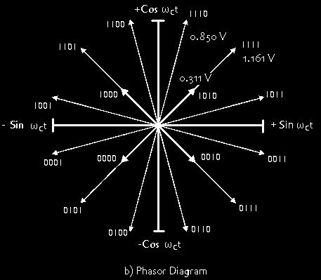
34 Advantages: Since efficient spectrum utilization is needed to maximize the number of users in a multi-user communication system, the low pass filter is used to restrict the bandwidth allowed to non-return-to-zero (NRZ) baseband signal. Since 90% of the power of the waveform is associated with the principle lobe, the low pass filter suppresses all other spectrum. Disadvantages: When multiplexing is done using BPSK using different carrier frequency for different baseband signal, the overlapping of spectra of various signal causes inter-channel interference. The spectrum suppression distorts the signal and there is a partial overlap of a bit (symbol) with adjacent bits in a single channel to produce inter-symbol interference. It can be reduced by using equalizers in the receiver. Applications: BPSK is widely used in both military and commercial communication systems. Quaternary Phase Shift Keying (QPSK): It is also called as Quadrature phase shift keying. QPSK is another form of angle modulated, constant amplitude digital modulation technique. It is an M-ary encoding technique where N = 2 and M = 2 N = 4. Quaternary means 4. Since 4 different output phases are possible for a single carrier frequency, it is called as Quaternary phase shift keying. Since 4 quadrants are used to represent the 4 different combination of input signals in constellation diagram, it is also called as Quadrature phase shift keying. Since 4 different output phases are needed, there must be 4 different input conditions.
35 Since digital input to a QPSK modulator is a binary (base 2) signal, to produce 4 different input combinations, the modulator requires more than a single input bit to determine the output conditions. With two bits, there are 4 possible conditions: 00, 01, 10 and 11. With QPSK, the binary input data are combined into group of two bits called dibits. In modulator, each dibit code generates one of the 4 possible output phases: +45, +135, -45 and For each 2-bit dibit clocked into the modulator, a single output change occurs. The rate of change at the output (baud) is equal to the one half of input bit rate since two input bits produce one output phase change. For N = 2, Baud = (f b /N) = (f b /2). QPSK Transmitter: Two bits (a dibit) are clocked into the bit splitter. After both bits has been serially inputted, they are simultaneously parallel outputted. One bit is directed to I-channel and the other bit is directed to Q-channel. I-bit modulates a carrier that is in-phase with the reference oscillator, hence the name I for in-phase. Q-bit modulates a carrier that is 90 out of phase (in quadrature) with the reference carrier, hence the name Q for Quadrature channel. Once a dibit has been split into I and Q channels, the operation is same as in BPSK modulator.
36 Essentially, a QPSK modulator is a two BPSK modulators combined in parallel. For logic 1 input (+1V) and logic 0 input (-1V), two phases are possible at the output of I-balanced modulator (+Sin ω C t, - Sin ω C t) and two phases are possible at the output of a Q-balanced modulator (+Cos ω C t, - Cos ω C t). When the linear summer combines the two Quadrature signals (90 out of phase), there are 4 possible resultant phasors given by the expressions: +Sin ω C t + Cos ω C t, +Sin ω C t - Cos ω C t, -Sin ω C t + Cos ω C t and -Sin ω C t - Cos ω C t.
37 With QPSK, each of the 4 possible output phasors has exactly the same amplitude. Therefore, the binary information must be encoded entirely in the phase of the output signal.
38 This constant amplitude characteristic is the most important characteristic of PSK that distinguishes it from QAM. Figure 3.20 (b) shows that the angular separation between any two adjacent phasors in QPSK is 90. QPSK can undergo almost +45 or -45 shift in phase during transmission and still retain the correct encoded information when demodulated at the receiver. Bandwidth Considerations of QPSK: Since the input data is divided into two channels, the bit rate in either I/Q channel is equal to one half of the input bit rate (f b /2). Essentially the bit splitter stretches I and Q bits to twice their input bit length. The highest fundamental frequency present at the data input to I or Q balanced modulator is equal to one fourth of the input data rate (one half of f b /2 = f b /4). The output of I and Q modulators requires a minimum double sided Nyquist bandwidth is equal to one half of the incoming bit rate (f N = twice f b /4 = f b /2). With QPSK, a bandwidth compression is realized. So the minimum bandwidth is less than the incoming bit rate.
39 Since QPSK output signal does not change phase until 2 bits (a dibit) have been clocked into the bit splitter, the fastest output rate of change (baud) is equal to one half of input bit rate (f b /2). The minimum bandwidth is equal to the baud. The worst case input condition to I or Q balanced modulator is an alternative 1/0 pattern, which occurs when the binary input data have a 1100 repetitive pattern.
40 One cycle of fastest binary transition (a 1/0 sequence) in I/Q channel takes same time as 4 input data bits. The highest fundamental frequency at the input and the fastest rate of change at the output of balanced modulators is equal to one fourth of the incoming bit rate. The output of balanced modulator can be expressed mathematically as, QPSK output = Sin ω c t x Sin ω a t = Sin 2πf c t x Sin 2πf a t Carrier signal Modulating signal = Sin 2πf c t x Sin 2π(f b /4)t where f C is the reference carrier frequency in Hertz. f a is the maximum fundamental frequency of binary input in Hertz. By trigonometric identity, Sin A Sin B = (1/2) [Cos (A-B) Cos (A+B)] Therefore, QPSK output = (1/2) Cos [2π(f C (f b /4) )t] - (1/2) Cos [2π(f C + (f b /4) )t] The output frequency spectrum extends from (f C (f b /4) ) to (f C + (f b /4) ). The minimum bandwidth, f N = (f C + (f b /4)) - (f C (f b /4) ) = 2f b /8 = f b /4. Problem: For a QPSK modulator, with an input data rate (f b ) equal to 10 Mbps and the carrier frequency as 70 MHz, determine the minimum double sided Nyquist bandwidth and baud. Also compare the results with those achieved with BPSK modulator. Solution: Bit rate in both I and Q channels = f bi = f bq = f b /2 = 5 Mbps The highest fundamental frequency presented to either balanced modulator is f a = f bi /2 or f bq /2 = f b /4 = 2.5 MHz The output waveform from each balanced modulator is
41 QPSK output = Sin ω c t x Sin ω a t = Sin 2πf c t x Sin 2πf a t Carrier signal Modulating signal = Sin 2πf c t x Sin 2π(f b /4)t = (1/2) Cos [2π(f C (f b /4) )t] - (1/2) Cos [2π(f C + (f b /4) )t] = (1/2) Cos [2π(70-2.5)MHzt] - (1/2) Cos [2π( )MHzt] = (1/2) Cos [2π(67.5 )t] - (1/2) Cos [2π(72.5 )t] The Nyquist bandwidth is, B = = 5 MHz Symbol rate = bandwidth = 5 Mbaud The output frequency spectrum is, For same input bit rate, the minimum bandwidth required to pass output of QPSK modulator is equal to one half of that required for BPSK modulator. Therefore, the minimum bandwidth, B = f b /2 = 5 MHz QPSK Receiver: Figure 3.23 shows the block diagram of QPSK receiver. The power splitter directs the input QPSK signal to I and Q product detectors and carrier recovery circuit. The carrier recovery circuit reproduces the original transmit carrier oscillator signal.
42 The recovered carrier must be frequency and phase coherent with the transmit reference carrier. The QPSK signal is demodulated in I and Q product detectors, which generate the original I and Q data bits. The output of product detectors are fed to the bit combining circuit where they are converted from parallel I and Q data channels to a single binary output data stream. The incoming QPSK signal may be any one of 4 possible output phases. To illustrate the demodulation process, let the incoming QPSK signal be Sin ω C t + Cos ω C t. The received QPSK signal ( Sin ω C t + Cos ω C t) is one of the inputs to I product detector. The other input is recovered carrier, Sin ω C t. Then the output of I product detector is, I = ( Sin ω C t + Cos ω C t) x Sin ω C t = - Sin 2 ω C t + Sin ω C t Cos ω C t = (-1/2) (1 - Cos 2ω C t) + (1/2) Sin (ω C + ω C ) t + (1/2) (Sin (ω C - ω C ) t
43 = (-1/2) + (1/2) Cos 2ω C t + (1/2) Sin 2ω C t Filtered out Equals to zero = -(1/2) V represents Logic 0. The received QPSK signal ( Sin ω C t + Cos ω C t) is one of the inputs to Q product detector. The other input is recovered carrier shifted 90 in phase, Cos ω C t. Then the output of Q product detector is, I = ( Sin ω C t + Cos ω C t) x Cos ω C t QPSK input signal Carrier signal = Cos 2 ω C t - Sin ω C t Cos ω C t = (1/2) (1 + Cos 2ω C t) - (1/2) Sin (ω C + ω C ) t - (1/2) (Sin (ω C - ω C ) t = (1/2) + (1/2) Cos 2ω C t - (1/2) Sin 2ω C t Filtered out Equals to zero = (1/2) V represents Logic 1. The demodulated I and Q bits (0 and 1 respectively) correspond to the constellation diagram and truth table for QPSK modulator. Offset QPSK (OQPSK): OQPSK is a modified form of QPSK where the bit waveforms on I and Q channels are offset or shifted in phase from each other by one half a bit time. Since the changes in I channel occur at the mid points of Q channel bits and vice versa, there is never more than a single bit change in the dibit code and therefore there is never more than a 90 shift in the output phase. In conventional QPSK, a change in the input dibit from 00 to 11 or 10 to 01 causes a corresponding 180 shift in the output phase.
44 The advantage of OQPSK is the changes in the output phase occur at twice the data rate in either I or Q channels. Consequently the baud and minimum bandwidth are twice that of conventional QPSK for a given transmission bit rate. OQPSK is sometimes called as Offset-keyed QPSK.
45 Quadrature Amplitude Modulation (QAM): QAM is also a form of digital modulation similar to PSK except the digital information is contained in both amplitude and phase of the transmitted carrier. ASK and PSK are combined in such a way that the positions of the signaling elements in the constellation diagram are optimized to achieve greatest distance between the elements. This decreases the likelihood of one element being misinterpreted as another element. This reduces the likelihood of errors occurring. 8-QAM: 8-QAM is an M-ary encoding technique where M = 8. It is same as that of 8-PSK but it is not a constant amplitude signal. 8-QAM Transmitter: The difference between 8-PAK and 8-QAM is the omission of inverter between the C Channel and Q product modulator. The incoming data are divided into two groups of 3 bits (tribits) I, Q and C bit streams, each with a bit rate equal to one third of the incoming bit rate. I and Q bits determine the polarity of PAM signals at the output of 2 to 4 level converters and C channel determines the magnitude. Since C bit is fed uninverted to both I and Q channel 2 to 4 level converters, the magnitudes of I and Q PAM signals are always equal. Their polarities depend on the logic condition of I and Q bits and therefore may be different. Figure 3.25 (b) shows the identical truth table for I and Q 2 to -4 level converters. If Q = I = C = 0, 000 is the tribit input, the output amplitude and phase can be determined as follows. The input to I channel 2 to -4 level converter is I = C = 0. The input to Q channel 2 to -4 level converter is Q = C = 0. From the truth table, the output amplitude is V.
46 The output of I Channel product modulator is Sin ω C t and the output of Q channel product modulator is Cos ω C t. The linear summer output is given by, The procedure is same for remaining tribit codes 001, 010, 011, 100, 101, 110 and 111.
47
48 Bandwidth Considerations of 8-QAM: In 8-QAM, the bit rate in the I and Q channels is equal to the one-third of the input binary rate f b, which is same as in 8-PSK. As a result, the highest fundamental modulating frequency and fastest output rate of change in 8-QAM are the same as with 8-PSK. Therefore, f a = f b /6. The minimum bandwidth required for 8-QAM is f b /3, same as in 8-PSK. 8-QAM Receiver: 8-QAM receiver is almost identical to 8-PSK receiver. The only difference is in the PAM levels at the output of the product detectors and the binary signals at the output of the analog-to-digital converters. Since there are two transmit amplitudes possible with 8-QAM that are different from those achievable with 8-PSK, the four demodulated PAM levels in 8-QAM are different from those in 8-PSK. Therefore, the conversion rate factor for the analog-to-digital converters in 8-QAM must also be different. Also, with 8-QAM the binary output signals from the I channel analog-to-digital converter are the I and C bits, and the binary output signals from the Q channel analog-to-digital converter are the Q and C bits.
49 Figure 3.28 shows the block diagram of 8-QAM receiver. The power splitter directs the input 8-QAM signal to I and Q product detectors and carrier recovery circuit. The carrier recovery circuit reproduces the original transmit carrier oscillator signal. The recovered carrier must be frequency and phase coherent with the transmit reference carrier. The 8-QAM signal is demodulated in I and Q product detectors, which generate the original I and C data bits in the output of I channel analog to digital converter and I and Q data bits in the output of Q channel analog to digital converter. The output of ADC are fed to the bit combining circuit (parallel to serial converter) where they are converted from parallel I and Q data channels to a single binary output data stream (QIC data bits). 16-QAM: 16-QAM is an M-ary system where N = 4 and M=16. The input data are acted on in groups of four (2 4 = 16). Both the phase and the amplitude of the transmit carrier are varied, which is same as with 8-QAM.
50 16-QAM Transmitter: Figure 3.29(a) shows the block diagram of 16-QAM transmitter. The input binary data are divided into four channels: I, I',Q and Q'. The bit rate in each channel is equal to one-fourth of the input bit rate (f b /4). The four bits are serially clocked into the bit splitter; then they are outputted simultaneously and in parallel with the I, I',Q and Q' channels. The I and Q bits determine the polarity at the output of the 2-to-4-level converters (Logic 1 = positive and Logic 0 = negative). The I' and Q' bits determine the magnitude (Logic 1 = V and logic 0 = 0.22 V). Figure 3.29(b) shows the truth table for the I and Q channel 2-to-4 level converters.
51 Consequently, 2-to-4 level converters generate a 4-level PAM signal. Two polarities and two magnitudes are possible at the output of each 2-to-4 level converter. They are V, V, V and V. These PAM signals modulate the in-phase and quadrature carriers in the product modulators. Four outputs are possible for each product modulator. For the I product modulator, they are sin ωω c t, sin ωω c t, sin ωω c t and sin ω c t. For the Q product modulator, they are cos ωω c t, cos ωω c t, cos ωω c t and cos ω c t. The linear summer combines the outputs from the I and Q channel product modulators and produces the 16 output conditions necessary for 16-QAM. For a quadbit input 0000, I = I = Q = Q = 0. The inputs to I channel 2-to-4 level converter are I = I = 0. The inputs to Q channel 2-to-4 level converter are Q = Q = 0. The 2 inputs to I channel product modulator are I = Sin ω c t and the 2 inputs to Q channel product modulator are Q = Cos ω c t. Therefore, the summer output is given by, Output = Sin ω c t-0.22 Cos ω c t = Sin (ω C t ) The procedure is same for the remaining quad bit codes.
52
CHAPTER 2 DIGITAL MODULATION
 2.1 INTRODUCTION CHAPTER 2 DIGITAL MODULATION Referring to Equation (2.1), if the information signal is digital and the amplitude (lv of the carrier is varied proportional to the information signal, a
CHETTINAD COLLEGE OF ENGINEERING & TECHNOLOGY NH-67, TRICHY MAIN ROAD, PULIYUR, C.F , KARUR DT.
 CHETTINAD COLLEGE OF ENGINEERING & TECHNOLOGY NH-67, TRICHY MAIN ROAD, PULIYUR, C.F. 639 114, KARUR DT. DEPARTMENT OF ELECTRONICS AND COMMUNICATION ENGINEERING COURSE MATERIAL Subject Name: Digital Communication
Internal Examination I Answer Key DEPARTMENT OF CSE & IT. Semester: III Max.Marks: 100
 NH 67, Karur Trichy Highways, Puliyur C.F, 639 114 Karur District Internal Examination I Answer Key DEPARTMENT OF CSE & IT Branch & Section: II CSE & IT Date & Time: 06.08.15 & 3 Hours Semester: III Max.Marks:
CHAPTER 2. Instructor: Mr. Abhijit Parmar Course: Mobile Computing and Wireless Communication ( )
") CHAPTER 2 Instructor: Mr. Abhijit Parmar Course: Mobile Computing and Wireless Communication (2170710) Syllabus Chapter-2.3 Modulation Techniques Reasons for Choosing Encoding Techniques Digital data,
CHAPTER 2 Instructor: Mr. Abhijit Parmar Course: Mobile Computing and Wireless Communication (2170710) Syllabus Chapter-2.3 Modulation Techniques Reasons for Choosing Encoding Techniques Digital data,
EXPERIMENT WISE VIVA QUESTIONS
 EXPERIMENT WISE VIVA QUESTIONS Pulse Code Modulation: 1. Draw the block diagram of basic digital communication system. How it is different from analog communication system. 2. What are the advantages of
ECE5713 : Advanced Digital Communications
 ECE5713 : Advanced Digital Communications Bandpass Modulation MPSK MASK, OOK MFSK 04-May-15 Advanced Digital Communications, Spring-2015, Week-8 1 In-phase and Quadrature (I&Q) Representation Any bandpass
Wireless Communication Fading Modulation
 EC744 Wireless Communication Fall 2008 Mohamed Essam Khedr Department of Electronics and Communications Wireless Communication Fading Modulation Syllabus Tentatively Week 1 Week 2 Week 3 Week 4 Week 5
EE3723 : Digital Communications
 EE3723 : Digital Communications Week 8-9: Bandpass Modulation MPSK MASK, OOK MFSK 04-May-15 Muhammad Ali Jinnah University, Islamabad - Digital Communications - EE3723 1 In-phase and Quadrature (I&Q) Representation
SEN366 Computer Networks
 SEN366 Computer Networks Prof. Dr. Hasan Hüseyin BALIK (5 th Week) 5. Signal Encoding Techniques 5.Outline An overview of the basic methods of encoding digital data into a digital signal An overview of
College of information Technology Department of Information Networks Telecommunication & Networking I Chapter 5. Analog Transmission
 Analog Transmission 5.1 DIGITAL-TO-ANALOG CONVERSION Digital-to-analog conversion is the process of changing one of the characteristics of an analog signal based on the information in digital data. The
Data Communications and Networking (Module 2)
") Data Communications and Networking (Module 2) Chapter 5 Signal Encoding Techniques References: Book Chapter 5 Data and Computer Communications, 8th edition, by William Stallings 1 Outline Overview Encoding
Data Communications and Networking (Module 2) Chapter 5 Signal Encoding Techniques References: Book Chapter 5 Data and Computer Communications, 8th edition, by William Stallings 1 Outline Overview Encoding
Objectives. Presentation Outline. Digital Modulation Lecture 01
 Digital Modulation Lecture 01 Review of Analogue Modulation Introduction to Digital Modulation Techniques Richard Harris Objectives You will be able to: Classify the various approaches to Analogue Modulation
Digital Modulation Lecture 01. Review of Analogue Modulation Introduction to Digital Modulation Techniques Richard Harris
 Digital Modulation Lecture 01 Review of Analogue Modulation Introduction to Digital Modulation Techniques Richard Harris Objectives You will be able to: Classify the various approaches to Analogue Modulation
Digital to Digital Encoding
 MODULATION AND ENCODING Data must be transformed into signals to send them from one place to another Conversion Schemes Digital-to-Digital Analog-to-Digital Digital-to-Analog Analog-to-Analog Digital to
EE 400L Communications. Laboratory Exercise #7 Digital Modulation
 EE 400L Communications Laboratory Exercise #7 Digital Modulation Department of Electrical and Computer Engineering University of Nevada, at Las Vegas PREPARATION 1- ASK Amplitude shift keying - ASK - in
Physical Layer. Networks: Physical Layer 1
 Physical Layer Networks: Physical Layer 1 Physical Layer Part 1 Definitions Nyquist Theorem - noiseless Shannon s Result with noise Analog versus Digital Amplifier versus Repeater Networks: Physical Layer
 UNIT 2 DIGITAL COMMUNICATION DIGITAL COMMUNICATION-Introduction The techniques used to modulate digital information so that it can be transmitted via microwave, satellite or down a cable pair is different
Digital Modulation Schemes
 Digital Modulation Schemes 1. In binary data transmission DPSK is preferred to PSK because (a) a coherent carrier is not required to be generated at the receiver (b) for a given energy per bit, the probability
Universitas Sumatera Utara
 Amplitude Shift Keying & Frequency Shift Keying Aim: To generate and demodulate an amplitude shift keyed (ASK) signal and a binary FSK signal. Intro to Generation of ASK Amplitude shift keying - ASK -
Department of Electronics and Communication Engineering 1
 UNIT I SAMPLING AND QUANTIZATION Pulse Modulation 1. Explain in detail the generation of PWM and PPM signals (16) (M/J 2011) 2. Explain in detail the concept of PWM and PAM (16) (N/D 2012) 3. What is the
CS441 Mobile & Wireless Computing Communication Basics
 Department of Computer Science Southern Illinois University Carbondale CS441 Mobile & Wireless Computing Communication Basics Dr. Kemal Akkaya E-mail: kemal@cs.siu.edu Kemal Akkaya Mobile & Wireless Computing
Chapter 2. Physical Layer
 Chapter 2 Physical Layer Lecture 1 Outline 2.1 Analog and Digital 2.2 Transmission Media 2.3 Digital Modulation and Multiplexing 2.4 Transmission Impairment 2.5 Data-rate Limits 2.6 Performance Physical
EE 460L University of Nevada, Las Vegas ECE Department
 EE 460L PREPARATION 1- ASK Amplitude shift keying - ASK - in the context of digital communications is a modulation process which imparts to a sinusoid two or more discrete amplitude levels. These are related
9.4. Synchronization:
 9.4. Synchronization: It is the process of timing the serial transmission to properly identify the data being sent. There are two most common modes: Synchronous transmission: Synchronous transmission relies
ELEC3242 Communications Engineering Laboratory Frequency Shift Keying (FSK)
") ELEC3242 Communications Engineering Laboratory 1 ---- Frequency Shift Keying (FSK) 1) Frequency Shift Keying Objectives To appreciate the principle of frequency shift keying and its relationship to analogue
ELEC3242 Communications Engineering Laboratory 1 ---- Frequency Shift Keying (FSK) 1) Frequency Shift Keying Objectives To appreciate the principle of frequency shift keying and its relationship to analogue
Review of Lecture 2. Data and Signals - Theoretical Concepts. Review of Lecture 2. Review of Lecture 2. Review of Lecture 2. Review of Lecture 2
 Data and Signals - Theoretical Concepts! What are the major functions of the network access layer? Reference: Chapter 3 - Stallings Chapter 3 - Forouzan Study Guide 3 1 2! What are the major functions
Signal Encoding Techniques
 2 Techniques ITS323: to Data Communications CSS331: Fundamentals of Data Communications Sirindhorn International Institute of Technology Thammasat University Prepared by Steven Gordon on 3 August 2015
Amplitude Modulation II
 Lecture 6: Amplitude Modulation II EE 3770: Communication Systems Lecture 6 Amplitude Modulation II AM Limitations DSB-SC Modulation SSB Modulation VSB Modulation Multiplexing Mojtaba Vaezi 6-1 Contents
Narrowband Data Transmission ASK/FSK
 Objectives Communication Systems II - Laboratory Experiment 9 Narrowband Data Transmission ASK/FSK To generate amplitude-shift keyed (ASK) and frequency-shift keyed (FSK) signals, study their properties,
AM Limitations. Amplitude Modulation II. DSB-SC Modulation. AM Modifications
 Lecture 6: Amplitude Modulation II EE 3770: Communication Systems AM Limitations AM Limitations DSB-SC Modulation SSB Modulation VSB Modulation Lecture 6 Amplitude Modulation II Amplitude modulation is
Lecture 3 Concepts for the Data Communications and Computer Interconnection
 Lecture 3 Concepts for the Data Communications and Computer Interconnection Aim: overview of existing methods and techniques Terms used: -Data entities conveying meaning (of information) -Signals data
Downloaded from 1
 VII SEMESTER FINAL EXAMINATION-2004 Attempt ALL questions. Q. [1] How does Digital communication System differ from Analog systems? Draw functional block diagram of DCS and explain the significance of
COMPUTER COMMUNICATION AND NETWORKS ENCODING TECHNIQUES
 COMPUTER COMMUNICATION AND NETWORKS ENCODING TECHNIQUES Encoding Coding is the process of embedding clocks into a given data stream and producing a signal that can be transmitted over a selected medium.
UNIT TEST I Digital Communication
 Time: 1 Hour Class: T.E. I & II Max. Marks: 30 Q.1) (a) A compact disc (CD) records audio signals digitally by using PCM. Assume the audio signal B.W. to be 15 khz. (I) Find Nyquist rate. (II) If the Nyquist
Data Encoding g(p (part 2)
") Data Encoding g(p (part 2) CSE 3213 Instructor: U.T. Nguyen 10/11/2007 12:44 PM 1 Analog Data, Digital Signals (5.3) 2 1 Analog Data, Digital Signals Digitization Conversion of analog data into digital
Data Encoding g(p (part 2) CSE 3213 Instructor: U.T. Nguyen 10/11/2007 12:44 PM 1 Analog Data, Digital Signals (5.3) 2 1 Analog Data, Digital Signals Digitization Conversion of analog data into digital
Outline. Communications Engineering 1
 Outline Introduction Signal, random variable, random process and spectra Analog modulation Analog to digital conversion Digital transmission through baseband channels Signal space representation Optimal
Modulation is the process of impressing a low-frequency information signal (baseband signal) onto a higher frequency carrier signal
 onto a higher frequency carrier signal") Modulation is the process of impressing a low-frequency information signal (baseband signal) onto a higher frequency carrier signal Modulation is a process of mixing a signal with a sinusoid to produce
Modulation is the process of impressing a low-frequency information signal (baseband signal) onto a higher frequency carrier signal Modulation is a process of mixing a signal with a sinusoid to produce
Signal Encoding Techniques
 Signal Encoding Techniques Overview Have already noted previous chapters that both analog and digital information can be encoded as either analog or digital signals: Digital data, digital signals: simplest
CSE 461 Bits and Links. David Wetherall
 CSE 461 Bits and Links David Wetherall djw@cs.washington.edu Topic How do we send a message across a wire or wireless link? The physical/link layers: 1. Different kinds of media 2. Fundamental limits 3.
Thus there are three basic modulation techniques: 1) AMPLITUDE SHIFT KEYING 2) FREQUENCY SHIFT KEYING 3) PHASE SHIFT KEYING
 AMPLITUDE SHIFT KEYING 2) FREQUENCY SHIFT KEYING 3) PHASE SHIFT KEYING") CHAPTER 5 Syllabus 1) Digital modulation formats 2) Coherent binary modulation techniques 3) Coherent Quadrature modulation techniques 4) Non coherent binary modulation techniques. Digital modulation formats:
CHAPTER 5 Syllabus 1) Digital modulation formats 2) Coherent binary modulation techniques 3) Coherent Quadrature modulation techniques 4) Non coherent binary modulation techniques. Digital modulation formats:
DIGITAL COMMUNICATIONS SYSTEMS. MSc in Electronic Technologies and Communications
 DIGITAL COMMUNICATIONS SYSTEMS MSc in Electronic Technologies and Communications Bandpass binary signalling The common techniques of bandpass binary signalling are: - On-off keying (OOK), also known as
QUESTION BANK SUBJECT: DIGITAL COMMUNICATION (15EC61)
") QUESTION BANK SUBJECT: DIGITAL COMMUNICATION (15EC61) Module 1 1. Explain Digital communication system with a neat block diagram. 2. What are the differences between digital and analog communication systems?
QUESTION BANK SUBJECT: DIGITAL COMMUNICATION (15EC61) Module 1 1. Explain Digital communication system with a neat block diagram. 2. What are the differences between digital and analog communication systems?
Announcements : Wireless Networks Lecture 3: Physical Layer. Bird s Eye View. Outline. Page 1
 Announcements 18-759: Wireless Networks Lecture 3: Physical Layer Please start to form project teams» Updated project handout is available on the web site Also start to form teams for surveys» Send mail
 DEPARTMENT OF COMPUTER GCE@Bodi_ SCIENCE GCE@Bodi_ AND ENIGNEERING GCE@Bodi_ GCE@Bodi_ GCE@Bodi_ Analog and Digital Communication GCE@Bodi_ DEPARTMENT OF CsE Subject Name: Analog and Digital Communication
Wireless Communications
 2. Physical Layer DIN/CTC/UEM 2018 Periodic Signal Periodic signal: repeats itself in time, that is g(t) = g(t + T ) in which T (given in seconds [s]) is the period of the signal g(t) The number of cycles
FDM- FREQUENCY DIVISION MULTIPLEXING
 FDM- FREQUENCY DIVISION MULTIPLEXING Multiplexing to refer to the combination of information streams from multiple sources for transmission over a shared medium Demultiplexing to refer to the separation
COSC 3213: Computer Networks I: Chapter 3 Handout #4. Instructor: Dr. Marvin Mandelbaum Department of Computer Science York University Section A
 COSC 3213: Computer Networks I: Chapter 3 Handout #4 Instructor: Dr. Marvin Mandelbaum Department of Computer Science York University Section A Topics: 1. Line Coding: Unipolar, Polar,and Inverted ; Bipolar;
Department of Electronic and Information Engineering. Communication Laboratory
 Department of Electronic and Information Engineering Communication Laboratory Frequency Shift Keying (FSK) & Differential Phase Shift Keying (DPSK) & Differential Quadrature Phase Shift Keying (DQPSK)
Chapter-15. Communication systems -1 mark Questions
 Chapter-15 Communication systems -1 mark Questions 1) What are the three main units of a Communication System? 2) What is meant by Bandwidth of transmission? 3) What is a transducer? Give an example. 4)
Department of Electronics & Telecommunication Engg. LAB MANUAL. B.Tech V Semester [ ] (Branch: ETE)
![Department of Electronics & Telecommunication Engg. LAB MANUAL. B.Tech V Semester [ ] (Branch: ETE)](/thumbs/86/93078052.jpg "Department of Electronics & Telecommunication Engg. LAB MANUAL. B.Tech V Semester [ ] (Branch: ETE)") Department of Electronics & Telecommunication Engg. LAB MANUAL SUBJECT:-DIGITAL COMMUNICATION SYSTEM [BTEC-501] B.Tech V Semester [2013-14] (Branch: ETE) KCT COLLEGE OF ENGG & TECH., FATEHGARH PUNJAB TECHNICAL
Department of Electronics & Telecommunication Engg. LAB MANUAL SUBJECT:-DIGITAL COMMUNICATION SYSTEM [BTEC-501] B.Tech V Semester [2013-14] (Branch: ETE) KCT COLLEGE OF ENGG & TECH., FATEHGARH PUNJAB TECHNICAL
Class 4 ((Communication and Computer Networks))
)") Class 4 ((Communication and Computer Networks)) Lesson 5... SIGNAL ENCODING TECHNIQUES Abstract Both analog and digital information can be encoded as either analog or digital signals. The particular encoding
Class 4 ((Communication and Computer Networks)) Lesson 5... SIGNAL ENCODING TECHNIQUES Abstract Both analog and digital information can be encoded as either analog or digital signals. The particular encoding
AN INTRODUCTION OF ANALOG AND DIGITAL MODULATION TECHNIQUES IN COMMUNICATION SYSTEM
 AN INTRODUCTION OF ANALOG AND DIGITAL MODULATION TECHNIQUES IN COMMUNICATION SYSTEM Rashmi Pandey Vedica Institute of Technology, Bhopal Department of Electronics & Communication rashmipandey07@rediffmail.com
Digital modulation techniques
 Outline Introduction Signal, random variable, random process and spectra Analog modulation Analog to digital conversion Digital transmission through baseband channels Signal space representation Optimal
Point-to-Point Communications
 Point-to-Point Communications Key Aspects of Communication Voice Mail Tones Alphabet Signals Air Paper Media Language English/Hindi English/Hindi Outline of Point-to-Point Communication 1. Signals basic
INTRODUCTION TO COMMUNICATION SYSTEMS AND TRANSMISSION MEDIA
 COMM.ENG INTRODUCTION TO COMMUNICATION SYSTEMS AND TRANSMISSION MEDIA 9/9/2017 LECTURES 1 Objectives To give a background on Communication system components and channels (media) A distinction between analogue
CSEP 561 Bits and Links. David Wetherall
 CSEP 561 Bits and Links David Wetherall djw@cs.washington.edu Topic How do we send a message across a wire or wireless link? The physical/link layers: 1. Different kinds of media 2. Fundamental limits
(Refer Slide Time: 2:23)
") Data Communications Prof. A. Pal Department of Computer Science & Engineering Indian Institute of Technology, Kharagpur Lecture-11B Multiplexing (Contd.) Hello and welcome to today s lecture on multiplexing
Data Communications Prof. A. Pal Department of Computer Science & Engineering Indian Institute of Technology, Kharagpur Lecture-11B Multiplexing (Contd.) Hello and welcome to today s lecture on multiplexing
Communications I (ELCN 306)
") Communications I (ELCN 306) c Samy S. Soliman Electronics and Electrical Communications Engineering Department Cairo University, Egypt Email: samy.soliman@cu.edu.eg Website: http://scholar.cu.edu.eg/samysoliman
Communications I (ELCN 306) c Samy S. Soliman Electronics and Electrical Communications Engineering Department Cairo University, Egypt Email: samy.soliman@cu.edu.eg Website: http://scholar.cu.edu.eg/samysoliman
Outline / Wireless Networks and Applications Lecture 3: Physical Layer Signals, Modulation, Multiplexing. Cartoon View 1 A Wave of Energy
 Outline 18-452/18-750 Wireless Networks and Applications Lecture 3: Physical Layer Signals, Modulation, Multiplexing Peter Steenkiste Carnegie Mellon University Spring Semester 2017 http://www.cs.cmu.edu/~prs/wirelesss17/
DIGITAL COMMUNICATION
 DIGITAL COMMUNICATION TRAINING LAB Digital communication has emerged to augment or replace the conventional analog systems, which had been used widely a few decades back. Digital communication has demonstrated
28. What is meant by repetition rate of the AM envelope? (ADC,AU-2010) 29. Describe the upper and lower sidebands. (ADC, AU-2010) 30.
 29. Describe the upper and lower sidebands. (ADC, AU-2010) 30.") Institute of Road and Transport Technology, Erode Department of Electronics and Communication Engineering Class/Sem: 2 nd Year Information Technology-3rd Semester Subject: Principles of Communication (IT)
Institute of Road and Transport Technology, Erode Department of Electronics and Communication Engineering Class/Sem: 2 nd Year Information Technology-3rd Semester Subject: Principles of Communication (IT)
RF/IF Terminology and Specs
 RF/IF Terminology and Specs Contributors: Brad Brannon John Greichen Leo McHugh Eamon Nash Eberhard Brunner 1 Terminology LNA - Low-Noise Amplifier. A specialized amplifier to boost the very small received
Department of Electronic and Information Engineering. Communication Laboratory. Phase Shift Keying (PSK) & Quadrature Phase Shift Keying (QPSK)
 & Quadrature Phase Shift Keying (QPSK)") Department of Electronic and Information Engineering Communication Laboratory Phase Shift Keying (PSK) & Quadrature Phase Shift Keying (QPSK) Objectives To familiar with the concept of describing phase
Department of Electronic and Information Engineering Communication Laboratory Phase Shift Keying (PSK) & Quadrature Phase Shift Keying (QPSK) Objectives To familiar with the concept of describing phase
B.Tech II Year II Semester (R13) Supplementary Examinations May/June 2017 ANALOG COMMUNICATION SYSTEMS (Electronics and Communication Engineering)
 Supplementary Examinations May/June 2017 ANALOG COMMUNICATION SYSTEMS (Electronics and Communication Engineering)") Code: 13A04404 R13 B.Tech II Year II Semester (R13) Supplementary Examinations May/June 2017 ANALOG COMMUNICATION SYSTEMS (Electronics and Communication Engineering) Time: 3 hours Max. Marks: 70 PART A
Code: 13A04404 R13 B.Tech II Year II Semester (R13) Supplementary Examinations May/June 2017 ANALOG COMMUNICATION SYSTEMS (Electronics and Communication Engineering) Time: 3 hours Max. Marks: 70 PART A
UNIT-2 Angle Modulation System
 UNIT-2 Angle Modulation System Introduction There are three parameters of a carrier that may carry information: Amplitude Frequency Phase Frequency Modulation Power in an FM signal does not vary with modulation
Chapter 5 Analog Transmission
 5-1 DIGITAL-TO-ANALOG CONVERSION Chapter 5 Analog Transmission Digital-to-analog conversion is the process of changing one of the characteristics of an analog signal depending on the information in digital
CSCD 433 Network Programming Fall Lecture 5 Physical Layer Continued
 CSCD 433 Network Programming Fall 2016 Lecture 5 Physical Layer Continued 1 Topics Definitions Analog Transmission of Digital Data Digital Transmission of Analog Data Multiplexing 2 Different Types of
ELEC3242 Communications Engineering Laboratory Amplitude Modulation (AM)
") ELEC3242 Communications Engineering Laboratory 1 ---- Amplitude Modulation (AM) 1. Objectives 1.1 Through this the laboratory experiment, you will investigate demodulation of an amplitude modulated (AM)
ELEC3242 Communications Engineering Laboratory 1 ---- Amplitude Modulation (AM) 1. Objectives 1.1 Through this the laboratory experiment, you will investigate demodulation of an amplitude modulated (AM)
Introduction to Communications Part Two: Physical Layer Ch3: Data & Signals
 Introduction to Communications Part Two: Physical Layer Ch3: Data & Signals Kuang Chiu Huang TCM NCKU Spring/2008 Goals of This Class Through the lecture of fundamental information for data and signals,
Overview. Chapter 4. Design Factors. Electromagnetic Spectrum
 Chapter 4 Transmission Media Overview Guided - wire Unguided - wireless Characteristics and quality determined by medium and signal For guided, the medium is more important For unguided, the bandwidth
CPSC Network Programming. How do computers really communicate?
 CPSC 360 - Network Programming Data Transmission Michele Weigle Department of Computer Science Clemson University mweigle@cs.clemson.edu February 11, 2005 http://www.cs.clemson.edu/~mweigle/courses/cpsc360
AM, PM and FM mo m dula l ti t o i n
 AM, PM and FM modulation What is amplitude modulation In order that a radio signal can carry audio or other information for broadcasting or for two way radio communication, it must be modulated or changed
2. TELECOMMUNICATIONS BASICS
 2. TELECOMMUNICATIONS BASICS The purpose of any telecommunications system is to transfer information from the sender to the receiver by a means of a communication channel. The information is carried by
Exercise 3-2. Digital Modulation EXERCISE OBJECTIVE DISCUSSION OUTLINE DISCUSSION. PSK digital modulation
 Exercise 3-2 Digital Modulation EXERCISE OBJECTIVE When you have completed this exercise, you will be familiar with PSK digital modulation and with a typical QPSK modulator and demodulator. DISCUSSION
CSCD 433 Network Programming Fall Lecture 5 Physical Layer Continued
 CSCD 433 Network Programming Fall 2016 Lecture 5 Physical Layer Continued 1 Topics Definitions Analog Transmission of Digital Data Digital Transmission of Analog Data Multiplexing 2 Different Types of
The quality of the transmission signal The characteristics of the transmission medium. Some type of transmission medium is required for transmission:
 Data Transmission The successful transmission of data depends upon two factors: The quality of the transmission signal The characteristics of the transmission medium Some type of transmission medium is
Lecture Outline. Data and Signals. Analogue Data on Analogue Signals. OSI Protocol Model
 Lecture Outline Data and Signals COMP312 Richard Nelson richardn@cs.waikato.ac.nz http://www.cs.waikato.ac.nz Analogue Data on Analogue Signals Digital Data on Analogue Signals Analogue Data on Digital
5.1 DIGITAL-TO-ANALOG CONVERSION
 CHAPTERS Analog Transmission n Chapter 3, we discussed the advantages and disadvantages of digital and analog transmission. We saw that while digital transmission is very desirable, a low-pass channel
C06a: Digital Modulation
 CISC 7332X T6 C06a: Digital Modulation Hui Chen Department of Computer & Information Science CUNY Brooklyn College 10/2/2018 CUNY Brooklyn College 1 Outline Digital modulation Baseband transmission Line
Signal Characteristics
 Data Transmission The successful transmission of data depends upon two factors:» The quality of the transmission signal» The characteristics of the transmission medium Some type of transmission medium
Chapter 12: Digital Modulation and Modems
 Chapter 12: Digital Modulation and Modems MULTIPLE CHOICE 1. FSK stands for: a. Full-Shift Keying c. Full-Signal Keying b. Frequency-Shift Keying d. none of the above 2. PSK stands for: a. Pulse-Signal
Basic Concepts in Data Transmission
 Basic Concepts in Data Transmission EE450: Introduction to Computer Networks Professor A. Zahid A.Zahid-EE450 1 Data and Signals Data is an entity that convey information Analog Continuous values within
 Modulations Analog Modulations Amplitude modulation (AM) Linear modulation Frequency modulation (FM) Phase modulation (PM) cos Angle modulation FM PM Digital Modulations ASK FSK PSK MSK MFSK QAM PAM Etc.
PRINCIPLES OF COMMUNICATION SYSTEMS. Lecture 1- Introduction Elements, Modulation, Demodulation, Frequency Spectrum
 PRINCIPLES OF COMMUNICATION SYSTEMS Lecture 1- Introduction Elements, Modulation, Demodulation, Frequency Spectrum Topic covered Introduction to subject Elements of Communication system Modulation General
Amplitude Frequency Phase
 Chapter 4 (part 2) Digital Modulation Techniques Chapter 4 (part 2) Overview Digital Modulation techniques (part 2) Bandpass data transmission Amplitude Shift Keying (ASK) Phase Shift Keying (PSK) Frequency
Speech, music, images, and video are examples of analog signals. Each of these signals is characterized by its bandwidth, dynamic range, and the
 Speech, music, images, and video are examples of analog signals. Each of these signals is characterized by its bandwidth, dynamic range, and the nature of the signal. For instance, in the case of audio
Introduction to Telecommunications and Computer Engineering Unit 3: Communications Systems & Signals
 Introduction to Telecommunications and Computer Engineering Unit 3: Communications Systems & Signals Syedur Rahman Lecturer, CSE Department North South University syedur.rahman@wolfson.oxon.org Acknowledgements
SUMMER 15 EXAMINATION. 1) The answers should be examined by key words and not as word-to-word as given in the
 The answers should be examined by key words and not as word-to-word as given in the") SUMMER 15 EXAMINATION Subject Code: 17535 Model Answer Important Instructions to examiners: 1) The answers should be examined by key words and not as word-to-word as given in the model answer scheme. 2)
SUMMER 15 EXAMINATION Subject Code: 17535 Model Answer Important Instructions to examiners: 1) The answers should be examined by key words and not as word-to-word as given in the model answer scheme. 2)
Communication Systems Lab
 LAB MANUAL Communication Systems Lab (EE-226-F) Prepared by: Varun Sharma (Lab In-charge) Dayal C. Sati (Faculty In-charge) B R C M CET BAHAL DEPARTMENT OF ELECTRONICS & COMMUNICATION ENGINEERING Page
Revision of Previous Six Lectures
 Revision of Previous Six Lectures Previous six lectures have concentrated on Modem, under ideal AWGN or flat fading channel condition Important issues discussed need to be revised, and they are summarised
Chapter 14 MODULATION INTRODUCTION
 Chapter 14 MODULATION INTRODUCTION As we have seen in previous three chapters, different types of media need different types of electromagnetic signals to carry information from the source to the destination.
Code No: R Set No. 1
 Code No: R05220405 Set No. 1 II B.Tech II Semester Regular Examinations, Apr/May 2007 ANALOG COMMUNICATIONS ( Common to Electronics & Communication Engineering and Electronics & Telematics) Time: 3 hours
Time division multiplexing The block diagram for TDM is illustrated as shown in the figure
 CHAPTER 2 Syllabus: 1) Pulse amplitude modulation 2) TDM 3) Wave form coding techniques 4) PCM 5) Quantization noise and SNR 6) Robust quantization Pulse amplitude modulation In pulse amplitude modulation,
Data Communications & Computer Networks
 Data Communications & Computer Networks Chapter 3 Data Transmission Fall 2008 Agenda Terminology and basic concepts Analog and Digital Data Transmission Transmission impairments Channel capacity Home Exercises
Analog Transmission CHAPTER
 CHAPTER 5 Analog Transmission n Chapter 3, we discussed the advantages and disadvantages of digital and analog transmission. We saw that while digital transmission is very desirable, a low-pass channel
Chapter 3 Digital Transmission Fundamentals
 Chapter 3 Digital Transmission Fundamentals Characterization of Communication Channels Fundamental Limits in Digital Transmission CSE 323, Winter 200 Instructor: Foroohar Foroozan Chapter 3 Digital Transmission
Angle Modulated Systems
 Angle Modulated Systems Angle of carrier signal is changed in accordance with instantaneous amplitude of modulating signal. Two types Frequency Modulation (FM) Phase Modulation (PM) Use Commercial radio
Data Conversion Circuits & Modulation Techniques. Subhasish Chandra Assistant Professor Department of Physics Institute of Forensic Science, Nagpur
 Data Conversion Circuits & Modulation Techniques Subhasish Chandra Assistant Professor Department of Physics Institute of Forensic Science, Nagpur Data Conversion Circuits 2 Digital systems are being used
Elements of Communication System Channel Fig: 1: Block Diagram of Communication System Terminology in Communication System
 Content:- Fundamentals of Communication Engineering : Elements of a Communication System, Need of modulation, electromagnetic spectrum and typical applications, Unit V (Communication terminologies in communication
Radio Technology and Architectures. 1 ENGN4521/ENGN6521: Embedded Wireless L#1
 Radio Technology and Architectures 1 ENGN4521/ENGN6521: Embedded Wireless L#1 Radio (Architectures) Spectrum plan and legal issues Radio Architectures and components 2 ENGN4521/ENGN6521: Embedded Wireless