Comparative Study of an Optical Link with PIN and APD as Photo-Detector Preetam Jain 1, Dr Lochan Jolly 2
|
|
|
- Ralph Armstrong
- 5 years ago
- Views:
Transcription
1 Comparative Study of an Optical Link with PIN and APD as Photo-Detector Preetam Jain 1, Dr Lochan Jolly 2 1 ME EXTC Student Thakur College of Engineering and Technology 2 Professor Thakur College of Engineering and Technology ABSTRACT Exchange of information between any two devices across a communication channel involves using some type of electrical or optical signal which carries the information. Parameters considered while analyzing the optical link are desired transmission distance, data rate or channel bandwidth and BER. This paper presents variation in the BER with the change in the transmission distance and the length of the fiber considering the photo-detector as PIN and APD. With the increase in length of the fiber and transmission data rate, dispersion increases. Hence, optical signal incident on the detector is below the required sensitivity power requirement and system is not able to give the electrical output. APD with single mode fiber gives the better performance over PIN. Keywords: PIN; APD; BER; Q-factor 1. INTRODUCTION Ever since ancient times, people had a principle need to communicate with one another. This need created interests in devicing communication system for sending messages from one distant place to another. Optical communication methods were of special interest among the many systems. The basic function of an optical fiber link is to transport a signal from communication equipment at one location to corresponding equipment at another location with a high degree of reliability and accuracy. While analyzing the link, parameters considered are desired transmission distance, data rate or channel bandwidth and BER [1]. The main constituents of an optical fiber communication link are transmitter consisting of optical source, an optical cable and a receiver consisting of a photo-detector. Photo-detector is the first element of the photo receiver circuit which interprets the information contained in the optical signal. They demodulate the optical signal that are subsequently amplified and processed to obtain the actual information signal. For such applications, photodetectors must have high sensitivity, high responsivity and minimum noise. In addition, the photo-detectors should be compact in size, use low biasing voltage and current, reliable under operating condition, and preferably integrated circuit compatible[2-9]. For high-bit-rate long-haul fiber optic communications, the avalanche photodiode (APD) is frequently the photo-detector of choice owing to its internal gain, which provides a sensitivity margin relative to PIN photodiodes. APDs can achieve 5 10-dB better sensitivity than PINs, provided that the multiplication noise is low and the gainbandwidth product is sufficiently high [10,11]. The single mode fiber has the advantage of low intermodal dispersion (broadening of transmitted light pulses), as only one mode is transmitted, whereas with multimode fiber dispersion may occur due to the differing group velocities of the propagating modes. This in turn restricts the maximum bandwidth attainable with multimode fibers, especially when compared with single mode fiber [1,2]. 2. THEORY The detector is an essential component of an optical fiber communication system and is one of the crucial elements which dictate the overall system performance. Its function is to convert the received optical signal into an electrical signal, which is then amplified before further processing. Therefore, when considering signal attenuation along the link, the system performance is determined at the detector. Improvement of detector characteristics and performance thus allows the installation of fewer repeater stations and lowers both the capital investments and maintenance costs. Requirements of the detectors are high sensitivity at the operating wavelength, high fidelity, large electrical response to the received optical signal, short response time to obtain a suitable bandwidth, minimum noise introduced by the detector, small size, low bias voltage, high reliability and low cost. Semiconductor photodiodes with or without internal gain provide good performance and compatibility with relative low cost. These photodiodes are made from semi-conductors such as silicon, germanium and an increasing number of III-V alloys, all of which satisfy in various ways most of the detector requirements. They are therefore used in all major current optical fiber communication systems. 2.1 Optical Detection Principle Volume 3, Issue 8, August 2014 Page 85
2 The basic detection process in an intrinsic absorber is illustrated in Fig.1 which shows a p-n photodiode. This device is reverse biased and the electric field developed across the p-n junction sweeps mobile carriers (holes and electrons) to their respectively majority sides (p and n type material). A depletion region or layer is therefore created on either side of the junction. This barrier has the effect of stopping the majority carriers crossing the junction in the opposite direction to the field. However, the field accelerates minority carriers from both sides to the opposite side of the junction, forming the reverse leakage current of the diode. Thus intrinsic conditions are created in the depletion region. Fig.1. Operation of the p-n photodiode A photon incident in or near the depletion region of this device which has an energy greater than or equal to the band-gap energy E g of the fabricating material (i.e. hf (where h is Planck s constant and c is velocity of light in air )>E g ) will excite an electron from the valence band into the conduction band. This process leaves an empty hole in the valence band and is known as the photo-generation of an electron-hole (carrier) pair, as shown in Fig.1(a). Carrier pairs so generated near the junction are separated and swept (drift) under the influence of the electric field to produce a displacement by current in the external circuit in excess of any reverse leakage current (Fig.1(b)). Photo-generation and the separation of a carrier pair in the depletion region of this reverse biased p-n junction is illustrated in Fig.1(c). 3. TYPES OF PHOTO-DIODES 3.1 PIN Photo-diode In order to allow operation at longer wavelength where the light penetrates more deeply into the semiconductor material a wider depletion region is necessary. To achieve this the n type material is doped so lightly that it can be considered intrinsic, and to make low resistance contact a highly doped n type (n + ) layer is added. This creates a PIN structure, as may be seen in Fig.2 where all absorption takes place in the depletion region. 3.2 Avalanche Photo-diode The second major type of optical communications detector is the avalanche photodiode (APD). This has a more sophisticated structure than the PIN photodiode in order to create an extremely high electric field region as may be seen in Fig.3. Therefore, as well as the depletion region where most of the photons are absorbed and the primary carrier pairs generated there is high field region in which holes and electrons can acquire sufficient energy to excite new electron-hole pairs. This process is known as impact ionization and is the phenomenon that leads to avalanche breakdown in ordinary reverse biased diodes. It often requires high reverse bias voltages (50 to 400 V). Fig.2. PIN photodiode showing combined absorption and depletion Volume 3, Issue 8, August 2014 Page 86
3 Fig.3. Avalanche photodiode showing high electric field region APD can give carrier multiplication factors as great as Most of the III-V semiconductors have nearly equal value of electron and hole ionization rate and as a result the APDs made with these materials become very noisy. For silicon, the Si-APDs are comparatively less noisy. 4 PARAMETERS FOR PHOTO-DETECTOR ANALYSIS Conversion Efficiency Conversion efficiency is the ratio of electrons generated to incident photons. It is defined as ability of the photo-detector to convert received optical power into the electrical power. It is transparent with the variation in the transmission data rate and decreases with the decrease in the incident optical power on it. When incident optical power is below the required sensitivity of detector conversion efficiency is almost equal to zero. Bit Error Rate In telecommunication transmission, the bit error rate (BER) is the percentage of bits that have errors relative to the total number of bits received in a transmission, usually expressed as ten to a negative power. For example, a transmission might have a BER of 10-6, meaning that, out of 1,000,000 bits transmitted, one bit was in error. Fibers Multimode fibers are with a core diameter of around 50µm or greater, which is large enough to allow the propagation of many modes within the fiber core. Single mode fiber allows the propagation of only one transverse electromagnetic mode (typically HE 11 ), and hence the core diameter must be of 2 to 10µm. 5 METHODOLOGY USE IN THE WORK 5.1 Optical Link To Be Characterized Optical link which is characterized in this work is shown in Fig.5. This optical link consists of information source and optical source which is CW Lorentzian laser with the input power of 2mW at the transmitter side. It then consists of an optical fiber which is multimode fiber through which information is transmitted to the receiver side. Receiver section consists of preamplifier which amplifies the received signal followed by a filter which removes the unwanted signals. It then consists of photo-detector which converts the optical signal back to the electrical signal. Link characterization is done by varying transmission data rate and the length of the fiber which results in the variation of the bit error rate and Q-factor. Volume 3, Issue 8, August 2014 Page 87
 is RSoft's award-winning software tool for the design and simulation of optical communication systems at the signal propagation level.")
4 5.2 Tool To Be Used Fig.5. Optical Link This work includes characterization of an optical link with PIN and avalanche photo-detector with the variation in the data rate and length of the fiber. Optimization and Simulation Consulting (OPTSIM) is RSoft's award-winning software tool for the design and simulation of optical communication systems at the signal propagation level. Hence, OPTSIM is used for the characterization of link in this work. 6. RESULTS AND DISCUSSIONS Simulation is performed with the input power of 2mW at the transmitter side and results show the variation of the BER for various length of the fiber. Fig.6 shows the variations in eye pattern with the length of the fiber as 100km, 200km, 300km, 400km and 500km at the data rate of 10 and 20Gbps and 30Gbps. At the data rate of 10Gbps and 20Gbps with the length of fiber as 100km, 200km and 300km. the receiver input is above its sensitivity power requirement. Therefore, it is able to convert the received optical signal into the electrical signal. At the data rate of 30Gbps, the optical signal incident on the detector is below the required sensitivity power requirement because with the increase in the data rate dispersion along the length of the fiber increases and hence is not able to give the electrical output. With the increase in the length of the fiber to 400km, at the data rate of 10Gbps the receiver is input is above its sensitivity power requirement and it is able to convert the received optical signal into the electrical signal because dispersion is within the tolerable limits but at the data rate of 20Gbps, with the increase in length of the fiber, dispersion increases and hence, optical signal incident on the detector is below the required sensitivity power requirement and is not able to give the electrical output. Further, increase in length of the fiber dispersion increases and hence, at a data rate of 10Gbps only receiver input is below its sensitivity power requirement and is not able to give the electrical output. Fig.6 (a). Eye pattern for the length of fiber = 100km Volume 3, Issue 8, August 2014 Page 88

.")

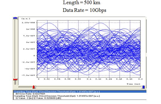
5 Fig.6 (b). Eye pattern for the length of fiber =200km Fig.6 (c). Eye pattern for the length of fiber =300km Fig.6 (d). Eye pattern for the length of fiber = 400km Fig.6 (e). Eye pattern for the length of fiber = 500km Volume 3, Issue 8, August 2014 Page 89
6 Further, increase in length of the fiber dispersion increases and hence, at a data rate of 10Gbps only receiver input is below its sensitivity power requirement and is not able to give the electrical output. Fig.7 shows graphical representation of BER versus length of the fiber with the variation in transmission data rate. B E R Q F a c t o r BER v/s Length Length(km) Q-factor v/s Length Data Rate=10Gbps Data Rate=20Gbps Data Rate=30Gbps Length(km) Fig.7. BER v/s Length and Q-factor v/s Length Conversion efficiency of photo-detector is independent of the length of the fiber is as shown in Fig.8. It decreases with the increase in data rate C o n v e r s i o n E f f i c i e n c y Conversion efficiency v/s Length Data Rate=10Gbps 0.1 Data Rate=20Gbps Data Rate=30Gbps Lenght(Km) Fig.8. Conversion Efficiency v/s Length Table1 shows BER and Q value with the PIN and Avalanche photo-diode when the fibers used are Single mode fiber (SMF) and Multi-mode fiber (MMF). It shows the SMF with the APD gives the better performance as compared to the PIN photo-diode because of the less dispersion in SMF and higher gain of the APD. Table 1. BER and Q-value for SMF and MMF Detector Type BER Q-Value D=8μm SMF D=80μm MMF D=8μm SMF D=80μm MMF PIN 1.48e e APD(Gain=2) 5.6e e APD(Gain=3) 9.2e-9 7e CONCLUSION From the various results obtained it can be concluded that PIN photodiode and APD cannot handle the transmission data rate beyond 30Gbps. At a data rate of 30Gbps and above, receiver input is below the sensitivity limit because with the increase in data rate dispersion along the length of the fiber increases. Therefore, it cannot effectively and reliably convert the optical signal to electrical signal. Length of the fiber between two nodes is limited by the rate of data transmission. The responsivity curve shows that different semiconductor materials can be used as detector material depending on the range of wavelengths used for transmission. Also, the result depict that conversion efficiency of any detector is Volume 3, Issue 8, August 2014 Page 90
7 independent of link length but dependent on data rate and mode of transmission. That is, SMF gives better quality factor signal at the receiver compared to MMF for same link length and data rate. REFERENCES [1] Gerd Keiser, Optical Fiber Communication, Tata McGraw Hill, 4 th Edition, [2] John M. Senior, Optical Fiber Communication, Pearson education limited, 3 rd Edition, [3] M.S.Tyagi, Introduction to Semiconductor Materials and Devices, John Wiley,1991. [4] Harold Kolimbiris, Fiber Optic Communication, Pearson Education,2004. [5] Bishnu P. Pal, Fundamentals of fiber optics in Tele-communication and Sensor Systems,New Age Limited,2 nd Edition,2009. [6] J. H. Franz, V. K. Jain, Optical Communication Components and Systems, Narosa Publishing House,2000. [7] J. Wilson, J. F. B. Hawkes, Optoelectronics An Introduction, Prentice Hall International Ltd.,1992. [8] S. M. Sze, Semiconductor Devices Physics and Technology, Wiley, 2 nd Edition, [9] Pallab Bhattacharya, Semi Optoelectronic Devices, Pearson Prentice Hall, 2 nd Edition,2006. [10] Joe C. Campbell, InP Recent Advances in Telecommunications Avalanche Photodiodes, Journal of light wave technology, Vol 25, pp , Jan [11] Daniel Hasko, Jaroslav Kovac, Frantisek Uherek, Jaroslava Skriniarova Jan Jakabovic Lorant Peternai, Design and Properties of InGaAS, InGaAsP, InP Avalanche photodiode, Journal of electrical engineering, Vol 58, pp , AUTHOR Taro Denshi received the B.S. and M.S. degrees in Electrical Engineering from Shibaura Institute of Technology in 1997 and 1999, respectively. During , he stayed in Communications Research Laboratory (CRL), Ministry of Posts and Telecommunications of Japan to study digital beam forming antennas, mobile satellite communication systems, and wireless access network using stratospheric platforms. He now with DDI Tokyo Pocket Telephone, Inc. Volume 3, Issue 8, August 2014 Page 91
Optical Receivers Theory and Operation
 Optical Receivers Theory and Operation Photo Detectors Optical receivers convert optical signal (light) to electrical signal (current/voltage) Hence referred O/E Converter Photodetector is the fundamental
Avalanche Photodiode. Instructor: Prof. Dietmar Knipp Presentation by Peter Egyinam. 4/19/2005 Photonics and Optical communicaton
 Avalanche Photodiode Instructor: Prof. Dietmar Knipp Presentation by Peter Egyinam 1 Outline Background of Photodiodes General Purpose of Photodiodes Basic operation of p-n, p-i-n and avalanche photodiodes
Chapter 3 OPTICAL SOURCES AND DETECTORS
 Chapter 3 OPTICAL SOURCES AND DETECTORS 3. Optical sources and Detectors 3.1 Introduction: The success of light wave communications and optical fiber sensors is due to the result of two technological breakthroughs.
Photodiode: LECTURE-5
 LECTURE-5 Photodiode: Photodiode consists of an intrinsic semiconductor sandwiched between two heavily doped p-type and n-type semiconductors as shown in Fig. 3.2.2. Sufficient reverse voltage is applied
OFCS OPTICAL DETECTORS 11/9/2014 LECTURES 1
 OFCS OPTICAL DETECTORS 11/9/2014 LECTURES 1 1-Defintion & Mechanisms of photodetection It is a device that converts the incident light into electrical current External photoelectric effect: Electrons are
UNIT III. By Ajay Kumar Gautam Asst. Prof. Electronics & Communication Engineering Dev Bhoomi Institute of Technology & Engineering, Dehradun
 UNIT III By Ajay Kumar Gautam Asst. Prof. Electronics & Communication Engineering Dev Bhoomi Institute of Technology & Engineering, Dehradun SYLLABUS Optical Absorption in semiconductors, Types of Photo
Detectors for Optical Communications
 Optical Communications: Circuits, Systems and Devices Chapter 3: Optical Devices for Optical Communications lecturer: Dr. Ali Fotowat Ahmady Sep 2012 Sharif University of Technology 1 Photo All detectors
Optical Amplifiers. Continued. Photonic Network By Dr. M H Zaidi
 Optical Amplifiers Continued EDFA Multi Stage Designs 1st Active Stage Co-pumped 2nd Active Stage Counter-pumped Input Signal Er 3+ Doped Fiber Er 3+ Doped Fiber Output Signal Optical Isolator Optical
Optical Fiber Communication Lecture 11 Detectors
 Optical Fiber Communication Lecture 11 Detectors Warriors of the Net Detector Technologies MSM (Metal Semiconductor Metal) PIN Layer Structure Semiinsulating GaAs Contact InGaAsP p 5x10 18 Absorption InGaAs
OPTOELECTRONIC and PHOTOVOLTAIC DEVICES
 OPTOELECTRONIC and PHOTOVOLTAIC DEVICES Outline 1. Introduction to the (semiconductor) physics: energy bands, charge carriers, semiconductors, p-n junction, materials, etc. 2. Light emitting diodes Light
Lecture 18: Photodetectors
 Lecture 18: Photodetectors Contents 1 Introduction 1 2 Photodetector principle 2 3 Photoconductor 4 4 Photodiodes 6 4.1 Heterojunction photodiode.................... 8 4.2 Metal-semiconductor photodiode................
Examination Optoelectronic Communication Technology. April 11, Name: Student ID number: OCT1 1: OCT 2: OCT 3: OCT 4: Total: Grade:
 Examination Optoelectronic Communication Technology April, 26 Name: Student ID number: OCT : OCT 2: OCT 3: OCT 4: Total: Grade: Declaration of Consent I hereby agree to have my exam results published on
Optical Communications
 Optical Communications Telecommunication Engineering School of Engineering University of Rome La Sapienza Rome, Italy 2005-2006 Lecture #4, May 9 2006 Receivers OVERVIEW Photodetector types: Photodiodes
Investigate the characteristics of PIN Photodiodes and understand the usage of the Lightwave Analyzer component.
 PIN Photodiode 1 OBJECTIVE Investigate the characteristics of PIN Photodiodes and understand the usage of the Lightwave Analyzer component. 2 PRE-LAB In a similar way photons can be generated in a semiconductor,
Lecture 9 External Modulators and Detectors
 Optical Fibres and Telecommunications Lecture 9 External Modulators and Detectors Introduction Where are we? A look at some real laser diodes. External modulators Mach-Zender Electro-absorption modulators
Unit 2 Semiconductor Devices. Lecture_2.5 Opto-Electronic Devices
 Unit 2 Semiconductor Devices Lecture_2.5 Opto-Electronic Devices Opto-electronics Opto-electronics is the study and application of electronic devices that interact with light. Electronics (electrons) Optics
Electronic devices-i. Difference between conductors, insulators and semiconductors
 Electronic devices-i Semiconductor Devices is one of the important and easy units in class XII CBSE Physics syllabus. It is easy to understand and learn. Generally the questions asked are simple. The unit
FIBER OPTICS. Prof. R.K. Shevgaonkar. Department of Electrical Engineering. Indian Institute of Technology, Bombay. Lecture: 20
 FIBER OPTICS Prof. R.K. Shevgaonkar Department of Electrical Engineering Indian Institute of Technology, Bombay Lecture: 20 Photo-Detectors and Detector Noise Fiber Optics, Prof. R.K. Shevgaonkar, Dept.
Fiber Optic Communication Link Design
 Fiber Optic Communication Link Design By Michael J. Fujita, S.K. Ramesh, PhD, Russell L. Tatro Abstract The fundamental building blocks of an optical fiber transmission link are the optical source, the
is a method of transmitting information from one place to another by sending light through an optical fiber. The light forms an electromagnetic
 is a method of transmitting information from one place to another by sending light through an optical fiber. The light forms an electromagnetic carrier wave that is modulated to carry information. The
Fiber Optic Communications Communication Systems
 INTRODUCTION TO FIBER-OPTIC COMMUNICATIONS A fiber-optic system is similar to the copper wire system in many respects. The difference is that fiber-optics use light pulses to transmit information down
SYLLABUS Optical Fiber Communication
 SYLLABUS Optical Fiber Communication Subject Code : IA Marks : 25 No. of Lecture Hrs/Week : 04 Exam Hours : 03 Total no. of Lecture Hrs. : 52 Exam Marks : 100 UNIT - 1 PART - A OVERVIEW OF OPTICAL FIBER
Design and Simulation of N-Substrate Reverse Type Ingaasp/Inp Avalanche Photodiode
 International Refereed Journal of Engineering and Science (IRJES) ISSN (Online) 2319-183X, (Print) 2319-1821 Volume 2, Issue 8 (August 2013), PP.34-39 Design and Simulation of N-Substrate Reverse Type
Chap14. Photodiode Detectors
 Chap14. Photodiode Detectors Mohammad Ali Mansouri-Birjandi mansouri@ece.usb.ac.ir mamansouri@yahoo.com Faculty of Electrical and Computer Engineering University of Sistan and Baluchestan (USB) Design
Prepared by: Dr. Rishi Prakash, Dept of Electronics and Communication Engineering Page 1 of 5
 Microwave tunnel diode Some anomalous phenomena were observed in diode which do not follows the classical diode equation. This anomalous phenomena was explained by quantum tunnelling theory. The tunnelling
Optodevice Data Book ODE I. Rev.9 Mar Opnext Japan, Inc.
 Optodevice Data Book ODE-408-001I Rev.9 Mar. 2003 Opnext Japan, Inc. Section 1 Operating Principles 1.1 Operating Principles of Laser Diodes (LDs) and Infrared Emitting Diodes (IREDs) 1.1.1 Emitting Principles
Review of Semiconductor Physics
 Review of Semiconductor Physics k B 1.38 u 10 23 JK -1 a) Energy level diagrams showing the excitation of an electron from the valence band to the conduction band. The resultant free electron can freely
Photon Count. for Brainies.
 Page 1/12 Photon Count ounting for Brainies. 0. Preamble This document gives a general overview on InGaAs/InP, APD-based photon counting at telecom wavelengths. In common language, telecom wavelengths
Figure Responsivity (A/W) Figure E E-09.
 Figure E E-09.") OSI Optoelectronics, is a leading manufacturer of fiber optic components for communication systems. The products offer range for Silicon, GaAs and InGaAs to full turnkey solutions. Photodiodes are semiconductor
OSI Optoelectronics, is a leading manufacturer of fiber optic components for communication systems. The products offer range for Silicon, GaAs and InGaAs to full turnkey solutions. Photodiodes are semiconductor
Data and Computer Communications. Tenth Edition by William Stallings
 Data and Computer Communications Tenth Edition by William Stallings Data and Computer Communications, Tenth Edition by William Stallings, (c) Pearson Education - Prentice Hall, 2013 Wireless Transmission
Key Questions ECE 340 Lecture 28 : Photodiodes
 Things you should know when you leave Key Questions ECE 340 Lecture 28 : Photodiodes Class Outline: How do the I-V characteristics change with illumination? How do solar cells operate? How do photodiodes
Measuring Photonic, Optoelectronic and Electro optic S parameters using an advanced photonic module
 Measuring Photonic, Optoelectronic and Electro optic S parameters using an advanced photonic module APPLICATION NOTE This application note describes the procedure for electro-optic measurements of both
Electronics devices and communication system. 1 MARK question:
 Electronics devices and communication system 1 MARK question: 1) In a transistor, doping level in base is increased slightly. How will it affect (i) collector current and (ii) base current? [Delhi 2011]
10/27/2009 Reading: Chapter 10 of Hambley Basic Device Physics Handout (optional)
") EE40 Lec 17 PN Junctions Prof. Nathan Cheung 10/27/2009 Reading: Chapter 10 of Hambley Basic Device Physics Handout (optional) Slide 1 PN Junctions Semiconductor Physics of pn junctions (for reference
EE40 Lec 17 PN Junctions Prof. Nathan Cheung 10/27/2009 Reading: Chapter 10 of Hambley Basic Device Physics Handout (optional) Slide 1 PN Junctions Semiconductor Physics of pn junctions (for reference
Figure Figure E E-09. Dark Current (A) 1.
 1.") OSI Optoelectronics, is a leading manufacturer of fiber optic components for communication systems. The products offer range for Silicon, GaAs and InGaAs to full turnkey solutions. Photodiodes are semiconductor
OSI Optoelectronics, is a leading manufacturer of fiber optic components for communication systems. The products offer range for Silicon, GaAs and InGaAs to full turnkey solutions. Photodiodes are semiconductor
UNIT-III SOURCES AND DETECTORS. According to the shape of the band gap as a function of the momentum, semiconductors are classified as
 UNIT-III SOURCES AND DETECTORS DIRECT AND INDIRECT BAND GAP SEMICONDUCTORS: According to the shape of the band gap as a function of the momentum, semiconductors are classified as 1. Direct band gap semiconductors
Determination of ideal Fibre Bragg Grating (FBG) length for Optical Transmission System
 length for Optical Transmission System") Determination of ideal Fibre Bragg Grating (FBG) length for Optical Transmission System Aastha Singhal SENSE school, VIT University Vellore, India Akanksha Singh SENSE school, VIT University Vellore, India
Determination of ideal Fibre Bragg Grating (FBG) length for Optical Transmission System Aastha Singhal SENSE school, VIT University Vellore, India Akanksha Singh SENSE school, VIT University Vellore, India
Fiber Optic Communication Systems. Unit-05: Types of Fibers. https://sites.google.com/a/faculty.muet.edu.pk/abdullatif
 Unit-05: Types of Fibers https://sites.google.com/a/faculty.muet.edu.pk/abdullatif Department of Telecommunication, MUET UET Jamshoro 1 Optical Fiber Department of Telecommunication, MUET UET Jamshoro
High-speed Ge photodetector monolithically integrated with large cross silicon-on-insulator waveguide
 [ APPLIED PHYSICS LETTERS ] High-speed Ge photodetector monolithically integrated with large cross silicon-on-insulator waveguide Dazeng Feng, Shirong Liao, Roshanak Shafiiha. etc Contents 1. Introduction
NON-AMPLIFIED PHOTODETECTOR USER S GUIDE
 NON-AMPLIFIED PHOTODETECTOR USER S GUIDE Thank you for purchasing your Non-amplified Photodetector. This user s guide will help answer any questions you may have regarding the safe use and optimal operation
OFC SYSTEM: Design Considerations. BC Choudhary, Professor NITTTR, Sector 26, Chandigarh.
 OFC SYSTEM: Design Considerations BC Choudhary, Professor NITTTR, Sector 26, Chandigarh. OFC point-to-point Link Transmitter Electrical to Optical Conversion Coupler Optical Fiber Coupler Optical to Electrical
Semiconductor Devices Lecture 5, pn-junction Diode
 Semiconductor Devices Lecture 5, pn-junction Diode Content Contact potential Space charge region, Electric Field, depletion depth Current-Voltage characteristic Depletion layer capacitance Diffusion capacitance
A silicon avalanche photodetector fabricated with standard CMOS technology with over 1 THz gain-bandwidth product
 A silicon avalanche photodetector fabricated with standard CMOS technology with over 1 THz gain-bandwidth product Myung-Jae Lee and Woo-Young Choi* Department of Electrical and Electronic Engineering,
NEW YORK CITY COLLEGE of TECHNOLOGY
 NEW YORK CITY COLLEGE of TECHNOLOGY THE CITY UNIVERSITY OF NEW YORK DEPARTMENT OF ELECTRICAL AND TELECOMMUNICATIONS ENGINEERING TECHNOLOGY Course : Prepared by: TCET 4102 Fiber-optic communications Module
Absorption: in an OF, the loss of Optical power, resulting from conversion of that power into heat.
 Absorption: in an OF, the loss of Optical power, resulting from conversion of that power into heat. Scattering: The changes in direction of light confined within an OF, occurring due to imperfection in
SIMULATIVE INVESTIGATION OF SINGLE-TONE ROF SYSTEM USING VARIOUS DUOBINARY MODULATION FORMATS
 SIMULATIVE INVESTIGATION OF SINGLE-TONE ROF SYSTEM USING VARIOUS DUOBINARY MODULATION FORMATS Namita Kathpal 1 and Amit Kumar Garg 2 1,2 Department of Electronics & Communication Engineering, Deenbandhu
Development of High Sensitivity SWIR APD Receivers
 Development of High Sensitivity SWIR APD Receivers Xiaogang Bai* a, Ping Yuan a, James Chang a, Rengarajan Sudharsanan a, Michael Krainak b, Guangning Yang b, Xiaoli Sun b, Wei Lu b, a Spectrolab Inc.,
Università degli Studi di Roma Tor Vergata Dipartimento di Ingegneria Elettronica. Analogue Electronics. Paolo Colantonio A.A.
 Università degli Studi di Roma Tor Vergata Dipartimento di Ingegneria Elettronica Analogue Electronics Paolo Colantonio A.A. 2015-16 Introduction: materials Conductors e.g. copper or aluminum have a cloud
OPTI510R: Photonics. Khanh Kieu College of Optical Sciences, University of Arizona Meinel building R.626
 OPTI510R: Photonics Khanh Kieu College of Optical Sciences, University of Arizona kkieu@optics.arizona.edu Meinel building R.626 Photodetectors Introduction Most important characteristics Photodetector
Photonics and Fiber Optics
 1 UNIT V Photonics and Fiber Optics Part-A 1. What is laser? LASER is the acronym for Light Amplification by Stimulated Emission of Radiation. The absorption and emission of light by materials has been
Analysis of Self Phase Modulation Fiber nonlinearity in Optical Transmission System with Dispersion
 36 Analysis of Self Phase Modulation Fiber nonlinearity in Optical Transmission System with Dispersion Supreet Singh 1, Kulwinder Singh 2 1 Department of Electronics and Communication Engineering, Punjabi
Optical Digital Transmission Systems. Xavier Fernando ADROIT Lab Ryerson University
 Optical Digital Transmission Systems Xavier Fernando ADROIT Lab Ryerson University Overview In this section we cover point-to-point digital transmission link design issues (Ch8): Link power budget calculations
Opto-electronic Receivers
 Purpose of a Receiver The receiver fulfils the function of optoelectronic conversion of an input optical signal into an output electrical signal (data stream). The purpose is to recover the data transmitted
Objective Type Questions 1. Why pure semiconductors are insulators at 0 o K? 2. What is effect of temperature on barrier voltage? 3.
 Objective Type Questions 1. Why pure semiconductors are insulators at 0 o K? 2. What is effect of temperature on barrier voltage? 3. What is difference between electron and hole? 4. Why electrons have
Resonant normal-incidence separate-absorptioncharge-multiplication. photodiodes
 Resonant normal-incidence separate-absorptioncharge-multiplication Ge/Si avalanche photodiodes Daoxin Dai 1*, Hui-Wen Chen 1, John E. Bowers 1 Yimin Kang 2, Mike Morse 2, Mario J. Paniccia 2 1 University
Downloaded from
 Question 14.1: In an n-type silicon, which of the following statement is true: (a) Electrons are majority carriers and trivalent atoms are the dopants. (b) Electrons are minority carriers and pentavalent
SRM UNIVERSITY FACULTY OF ENGINEERING AND TECHNOLOGY SCHOOL OF ELECTRONICS AND ELECTRICAL ENGINEERING DEPARTMENT OF TCE COURSE PLAN
 SRM UNIVERSITY FACULTY OF ENGINEERING AND TECHNOLOGY SCHOOL OF ELECTRONICS AND ELECTRICAL ENGINEERING DEPARTMENT OF TCE COURSE PLAN Course Code : TE1018 Course Title : Microwave Radio And Optical Fiber
Problem 4 Consider a GaAs p-n + junction LED with the following parameters at 300 K: Electron diusion coecient, D n = 25 cm 2 =s Hole diusion coecient
 Prof. Jasprit Singh Fall 2001 EECS 320 Homework 7 This homework is due on November 8. Problem 1 An optical power density of 1W/cm 2 is incident on a GaAs sample. The photon energy is 2.0 ev and there is
InP-based Waveguide Photodetector with Integrated Photon Multiplication
 InP-based Waveguide Photodetector with Integrated Photon Multiplication D.Pasquariello,J.Piprek,D.Lasaosa,andJ.E.Bowers Electrical and Computer Engineering Department University of California, Santa Barbara,
MOSFET short channel effects
 MOSFET short channel effects overview Five different short channel effects can be distinguished: velocity saturation drain induced barrier lowering (DIBL) impact ionization surface scattering hot electrons
ELECTRONIC DEVICES AND CIRCUITS
 ELECTRONIC DEVICES AND CIRCUITS 1. At room temperature the current in an intrinsic semiconductor is due to A. holes B. electrons C. ions D. holes and electrons 2. Work function is the maximum energy required
1) A silicon diode measures a low value of resistance with the meter leads in both positions. The trouble, if any, is
 A silicon diode measures a low value of resistance with the meter leads in both positions. The trouble, if any, is") 1) A silicon diode measures a low value of resistance with the meter leads in both positions. The trouble, if any, is A [ ]) the diode is open. B [ ]) the diode is shorted to ground. C [v]) the diode is
1) A silicon diode measures a low value of resistance with the meter leads in both positions. The trouble, if any, is A [ ]) the diode is open. B [ ]) the diode is shorted to ground. C [v]) the diode is
Performance Evaluation of 32 Channel DWDM System Using Dispersion Compensation Unit at Different Bit Rates
 Performance Evaluation of 32 Channel DWDM System Using Dispersion Compensation Unit at Different Bit Rates Simarpreet Kaur Gill 1, Gurinder Kaur 2 1Mtech Student, ECE Department, Rayat- Bahra University,
Lecture 7:PN Junction. Structure, Depletion region, Different bias Conditions, IV characteristics, Examples
 Lecture 7:PN Junction Structure, Depletion region, Different bias Conditions, IV characteristics, Examples PN Junction The diode (pn junction) is formed by dopping a piece of intrinsic silicon, such that
Sharjah Indian School, Sharjah ELECTRONIC DEVICES - Class XII (Boys Wing) Page 01
 Page 01") ELECTRONIC DEVICES - Class XII (Boys Wing) Page 01 Electronics is the fast developing branch of Physics. Before the discovery of transistors in 1948, vacuum tubes (thermionic valves) were used as the building
ELECTRONIC DEVICES - Class XII (Boys Wing) Page 01 Electronics is the fast developing branch of Physics. Before the discovery of transistors in 1948, vacuum tubes (thermionic valves) were used as the building
NON-AMPLIFIED HIGH SPEED PHOTODETECTOR USER S GUIDE
 NON-AMPLIFIED HIGH SPEED PHOTODETECTOR USER S GUIDE Thank you for purchasing your Non-amplified High Speed Photodetector. This user s guide will help answer any questions you may have regarding the safe
HIGH SPEED FIBER PHOTODETECTOR USER S GUIDE
 HIGH SPEED FIBER PHOTODETECTOR USER S GUIDE Thank you for purchasing your High Speed Fiber Photodetector. This user s guide will help answer any questions you may have regarding the safe use and optimal
ECE 340 Lecture 29 : LEDs and Lasers Class Outline:
 ECE 340 Lecture 29 : LEDs and Lasers Class Outline: Light Emitting Diodes Lasers Semiconductor Lasers Things you should know when you leave Key Questions What is an LED and how does it work? How does a
Guided Propagation Along the Optical Fiber
 Guided Propagation Along the Optical Fiber The Nature of Light Quantum Theory Light consists of small particles (photons) Wave Theory Light travels as a transverse electromagnetic wave Ray Theory Light
Optical Fiber Communication
 A Seminar report On Optical Fiber Communication Submitted in partial fulfillment of the requirement for the award of degree Of Mechanical SUBMITTED TO: www.studymafia.org SUBMITTED BY: www.studymafia.org
Key Questions. What is an LED and how does it work? How does a laser work? How does a semiconductor laser work? ECE 340 Lecture 29 : LEDs and Lasers
 Things you should know when you leave Key Questions ECE 340 Lecture 29 : LEDs and Class Outline: What is an LED and how does it How does a laser How does a semiconductor laser How do light emitting diodes
Semiconductor Optical Active Devices for Photonic Networks
 UDC 621.375.8:621.38:621.391.6 Semiconductor Optical Active Devices for Photonic Networks VKiyohide Wakao VHaruhisa Soda VYuji Kotaki (Manuscript received January 28, 1999) This paper describes recent
PHYSICAL ELECTRONICS(ECE3540) APPLICATIONS OF PHYSICAL ELECTRONICS PART I
 APPLICATIONS OF PHYSICAL ELECTRONICS PART I") PHYSICAL ELECTRONICS(ECE3540) APPLICATIONS OF PHYSICAL ELECTRONICS PART I Tennessee Technological University Monday, October 28, 2013 1 Introduction In the following slides, we will discuss the summary
PHYSICAL ELECTRONICS(ECE3540) APPLICATIONS OF PHYSICAL ELECTRONICS PART I Tennessee Technological University Monday, October 28, 2013 1 Introduction In the following slides, we will discuss the summary
Special Issue Review. 1. Introduction
 Special Issue Review In recently years, we have introduced a new concept of photonic antennas for wireless communication system using radio-over-fiber technology. The photonic antenna is a functional device
A-CUBE-Series High Sensitivity APD Detector Modules
 Series Description Laser Components new A-CUBE range of APD modules has been designed for customers interested in experimenting with APDs. Featuring a low-noise silicon (or InGaAs) APD with matched preamplifier
Performance Analysis of dispersion compensation using Fiber Bragg Grating (FBG) in Optical Communication
 in Optical Communication") Research Article International Journal of Current Engineering and Technology E-ISSN 2277 416, P-ISSN 2347-5161 214 INPRESSCO, All Rights Reserved Available at http://inpressco.com/category/ijcet Performance
Research Article International Journal of Current Engineering and Technology E-ISSN 2277 416, P-ISSN 2347-5161 214 INPRESSCO, All Rights Reserved Available at http://inpressco.com/category/ijcet Performance
Compensation of Dispersion in 10 Gbps WDM System by Using Fiber Bragg Grating
 International Journal of Computational Engineering & Management, Vol. 15 Issue 5, September 2012 www..org 16 Compensation of Dispersion in 10 Gbps WDM System by Using Fiber Bragg Grating P. K. Raghav 1,
Analyzing the Non-Linear Effects in DWDM Optical Network Using MDRZ Modulation Format
 Analyzing the Non-Linear Effects in DWDM Optical Network Using MDRZ Modulation Format Ami R. Lavingia Electronics & Communication Dept. SAL Institute of Technology & Engineering Research Gujarat Technological
EXAMINATION FOR THE DEGREE OF B.E. and M.E. Semester
 EXAMINATION FOR THE DEGREE OF B.E. and M.E. Semester 2 2009 101908 OPTICAL COMMUNICATION ENGINEERING (Elec Eng 4041) 105302 SPECIAL STUDIES IN MARINE ENGINEERING (Elec Eng 7072) Official Reading Time:
Simulation And Analysis of 10 Gbps APD Receiver with Dispersion Compensation
 Conference on Advances in Communication and Control Systems 2013 (CAC2S 2013) Simulation And Analysis of 10 Gbps APD Receiver with Dispersion Compensation Vyas Drasti Atul Department of Electronics and
Lecture 14: Photodiodes
 Lecture 14: Photodiodes Background concepts p-n photodiodes photoconductive/photovoltaic modes p-i-n photodiodes responsivity and bandwidth Reading: Senior 8.1-8.8.3 Keiser Chapter 6 1 Electron-hole photogeneration
Design of Ultra High Capacity DWDM System with Different Modulation Formats
 Design of Ultra High Capacity DWDM System with Different Modulation Formats A. Nandhini 1, K. Gokulakrishnan 2 1 PG Scholar, Department of Electronics & Communication Engineering, Regional Center, Anna
Measurement of Distortion in Multi-tone Modulation Fiber-based analog CATV Transmission System
 5 th SASTech 011, Khavaran Higher-education Institute, Mashhad, Iran. May 1-14. 1 Measurement of Distortion in Multi-tone Modulation Fiber-based analog CATV Transmission System Morteza Abdollahi Sharif
32-Channel DWDM System Design and Simulation by Using EDFA with DCF and Raman Amplifiers
 2012 International Conference on Information and Computer Networks (ICICN 2012) IPCSIT vol. 27 (2012) (2012) IACSIT Press, Singapore 32-Channel DWDM System Design and Simulation by Using EDFA with DCF
INGAAS FAST PIN (RF) AMPLIFIED PHOTODETECTORS
 AMPLIFIED PHOTODETECTORS") INGAAS FAST PIN (RF) AMPLIFIED PHOTODETECTORS High Signal-to-Noise Ratio Ultrafast up to 9.5 GHz Free-Space or Fiber-Coupled InGaAs Photodetectors Wavelength Range from 750-1650 nm FPD310 FPD510-F https://www.thorlabs.com/newgrouppage9_pf.cfm?guide=10&category_id=77&objectgroup_id=6687
INGAAS FAST PIN (RF) AMPLIFIED PHOTODETECTORS High Signal-to-Noise Ratio Ultrafast up to 9.5 GHz Free-Space or Fiber-Coupled InGaAs Photodetectors Wavelength Range from 750-1650 nm FPD310 FPD510-F https://www.thorlabs.com/newgrouppage9_pf.cfm?guide=10&category_id=77&objectgroup_id=6687
Lesson 08. Name and affiliation of the author: Professor L B D R P Wijesundera Department of Physics, University of Kelaniya.
 Lesson 08 Title of the Experiment: Identification of active components in electronic circuits and characteristics of a Diode, Zener diode and LED (Activity number of the GCE Advanced Level practical Guide
Measure the roll-off frequency of an acousto-optic modulator
 Slide 1 Goals of the Lab: Get to know some of the properties of pin photodiodes Measure the roll-off frequency of an acousto-optic modulator Measure the cut-off frequency of a pin photodiode as a function
Physics of Waveguide Photodetectors with Integrated Amplification
 Physics of Waveguide Photodetectors with Integrated Amplification J. Piprek, D. Lasaosa, D. Pasquariello, and J. E. Bowers Electrical and Computer Engineering Department University of California, Santa
Performance Analysis Of An Ultra High Capacity 1 Tbps DWDM-RoF System For Very Narrow Channel Spacing
 Performance Analysis Of An Ultra High Capacity 1 Tbps DWDM-RoF System For Very Narrow Channel Spacing Viyoma Sarup* and Amit Gupta Chandigarh University Punjab, India *viyoma123@gmail.com Abstract A RoF
for optical communication system
 High speed Ge waveguide detector for optical communication system Xingjun Wang, Zhijuan Tu and Zhiping Zhou State Key Laboratory of Advanced Optical Communication Systems and Networks, School of Electronics
LEDs, Photodetectors and Solar Cells
 LEDs, Photodetectors and Solar Cells Chapter 7 (Parker) ELEC 424 John Peeples Why the Interest in Photons? Answer: Momentum and Radiation High electrical current density destroys minute polysilicon and
 Electronic Devices 1. Current flowing in each of the following circuits A and respectively are: (Circuit 1) (Circuit 2) 1) 1A, 2A 2) 2A, 1A 3) 4A, 2A 4) 2A, 4A 2. Among the following one statement is not
Application of optical system simulation software in a fiber optic telecommunications program
 Rochester Institute of Technology RIT Scholar Works Presentations and other scholarship 2004 Application of optical system simulation software in a fiber optic telecommunications program Warren Koontz
Chapter 8. Digital Links
 Chapter 8 Digital Links Point-to-point Links Link Power Budget Rise-time Budget Power Penalties Dispersions Noise Content Photonic Digital Link Analysis & Design Point-to-Point Link Requirement: - Data
UNIT - 5 OPTICAL RECEIVER
 UNIT - 5 LECTURE-1 OPTICAL RECEIVER Introduction, Optical Receiver Operation, receiver sensitivity, quantum limit, eye diagrams, coherent detection, burst mode receiver operation, Analog receivers. RECOMMENDED
Fiberoptic Communication Systems By Dr. M H Zaidi. Optical Amplifiers
 Optical Amplifiers Optical Amplifiers Optical signal propagating in fiber suffers attenuation Optical power level of a signal must be periodically conditioned Optical amplifiers are a key component in
Available online at ScienceDirect. Procedia Computer Science 93 (2016 )
") Available online at www.sciencedirect.com ScienceDirect Procedia Computer Science 93 (016 ) 647 654 6th International Conference On Advances In Computing & Communications, ICACC 016, 6-8 September 016,
Available online at www.sciencedirect.com ScienceDirect Procedia Computer Science 93 (016 ) 647 654 6th International Conference On Advances In Computing & Communications, ICACC 016, 6-8 September 016,
Copyright -International Centre for Diffraction Data 2010 ISSN
 234 BRIDGING THE PRICE/PERFORMANCE GAP BETWEEN SILICON DRIFT AND SILICON PIN DIODE DETECTORS Derek Hullinger, Keith Decker, Jerry Smith, Chris Carter Moxtek, Inc. ABSTRACT Use of silicon drift detectors
Optical Sources and Detectors
 Optical Sources and Detectors 1. Optical Sources Optical transmitter coverts electrical input signal into corresponding optical signal. The optical signal is then launched into the fiber. Optical source
Basic concepts. Optical Sources (b) Optical Sources (a) Requirements for light sources (b) Requirements for light sources (a)
 Optical Sources (a) Requirements for light sources (b) Requirements for light sources (a)") Optical Sources (a) Optical Sources (b) The main light sources used with fibre optic systems are: Light-emitting diodes (LEDs) Semiconductor lasers (diode lasers) Fibre laser and other compact solid-state
Optical Sources (a) Optical Sources (b) The main light sources used with fibre optic systems are: Light-emitting diodes (LEDs) Semiconductor lasers (diode lasers) Fibre laser and other compact solid-state