Electronics: Design and Build Training Session. Presented By: Dr. Shakti Singh Hazem Elgabra Amna Siddiqui
|
|
|
- Maria Annabel Wells
- 5 years ago
- Views:
Transcription
1 Electronics: Design and Build Training Session Presented By: Dr. Shakti Singh Hazem Elgabra Amna Siddiqui
2 Basic prototyping and measurement tools
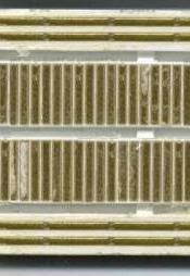
3 Breadboard basics Back View VCC GND VSS

 Beware of")
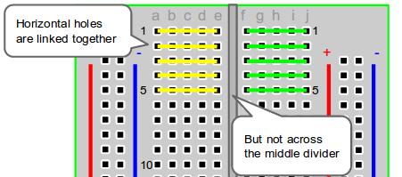
4 Breadboard basics (contd.) Beware of isolations!

5 Variable Power Supply Has 3 voltage sources (two variable and one fixed at 5 V) Don t play with these Can be used in 3 ways to create: 1. Two independent supply voltages 2. Two reference voltages for same circuit 3. +V and V Make sure always green! Fixed 5 V
6 Variable Power Supply (contd.) Two independent supply voltages Two reference voltages for same circuit +VCC and -VSS - - GND - V1 + - V2 + V1+ V2+ - V + V +3 V +5 V +3 V +5 V -3 V +3 V

7 Digital Multimeter (DMM) To measure voltage (connect in parallel):
 To measure current, disconnect nodes and")
8 Digital Multimeter (DMM) (contd.) To measure current, disconnect nodes and connect in series!

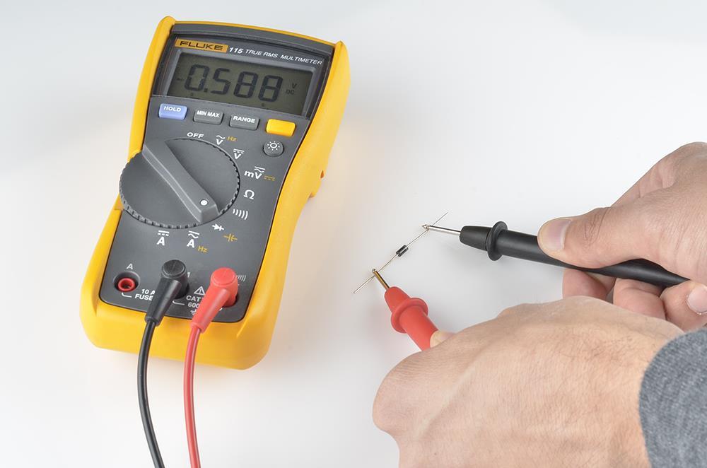
9 Digital Multimeter (DMM) (contd.) How to measure resistance?
10 Potentiometers 1 R1 = <10 kω 2 10 kω R2 = 10 kω R kω
 (contd.")

11 Digital Multimeter (DMM) (contd.) How to find out if two nodes are connected?
 + Vout - 1. Enter values for amplitude, frequency, offset etc. 2.")
12 Function Generator Can be used to simulate the analog inputs to your circuit 1. Select function to set (sine, square) + Vout - 1. Enter values for amplitude, frequency, offset etc. 2. Use keypad or knob 3. Make sure units are right!
 Measure (use F1-F4) Autoset (to reset viewing settings) - CH1 + -")
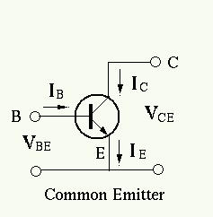
13 Oscilloscope (voltage signal viewer) Like voltmeter but for analog signals Can view up to two signals at a time (2 channels) Measure (use F1-F4) Autoset (to reset viewing settings) - CH1 + - CH2 +
 Increases/decreases voltage resolution for CH1 signal Increases/decreases voltage resolution for CH2 signal View/Hide signal at CH1")
14 Oscilloscope (contd.) Increases/decreases voltage resolution for CH1 signal Increases/decreases voltage resolution for CH2 signal View/Hide signal at CH1 Increases/decreases time resolution for both channels voltage Shift CH1 signal up or down Shift view right or left Shift CH2 signal up or down time
15 Oscilloscope (contd.) 3 Coupling modes DC coupling: show the signal as it is AC coupling: remove DC shift of the signal by setting the vertical zero point to (signal max + signal min) / 2 This is a modified version of your signal! It will show any battery s voltage as ZERO GND coupling: just shows zero
16 DC Motor
17 DC Motor
18 DC Motor
19 DC Motor
20 DC Motor
21 DC Motor
22 DC Motor
23 DC Motor
24 DC Motor To increase speed, increase voltage With increased voltage, you draw more current No worries when connected directly to a power supply

25 DC Motor To increase speed, increase voltage With increased voltage, you draw more current No worries when connected directly to a power supply

26 DC Motor But what happens when it is integrated within a circuit?
27 DC Motor If the motor is turning that doesn t mean that it is working as you want yet The motor will have to move something which will resist it (because physics) The more resistance it faces the more current it requires If your circuit cannot support the extra current, the motor will simply stop
28 Datasheets
29 Part number What is it Some chips tell you what are they made for Chip pin out Pins description Quick description
30 Comprehensive symbol Chip pin out Pins description

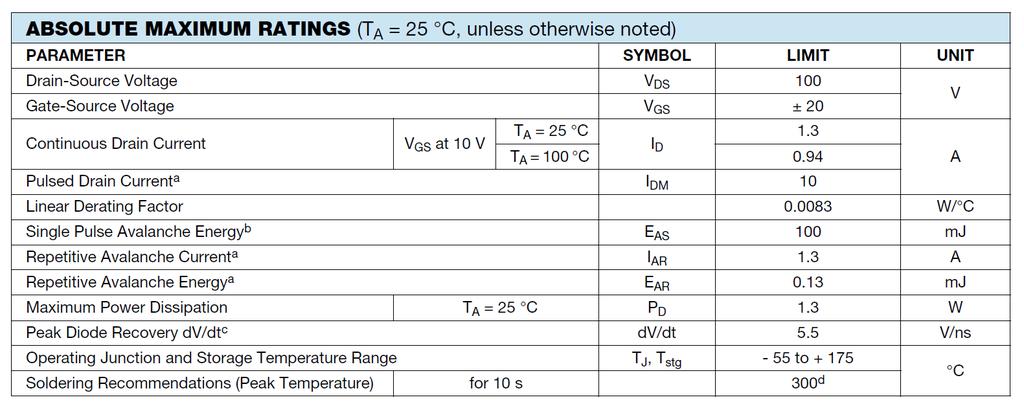
31 Rating values i.e. maximum supply voltage is 36 V Some datasheets have recommended conditions
32
33

34 Specifications Rating values i.e. maximum supply voltage is +/- 22V Sometimes the datasheet is for a series of similar components Will have everything you might need
35 Comprehensive symbol Inner circuit
36 Will always show the inner circuit
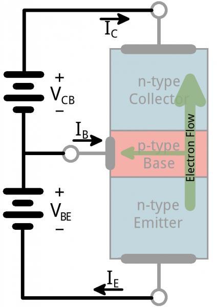
37 Transistors
38 Diodes The main function of a diode is to control the direction of control flow. Current only flows in forward direction, in reverse the current is blocked. ideal diode
39 Diodes Forward Bias Reverse Bias
 in order for the current to be anything significant. 2.")
40 Diodes Real Diode 1.Forward bias: When the voltage across the diode is positive the diode is on and current can run through. The voltage should be greater than the forward voltage (V F ) in order for the current to be anything significant. 2.Reverse bias: This is the off mode of the diode, where the voltage is less than V F but greater than -V BR. In this mode current flow is (mostly) blocked, and the diode is off. A very small amount of current (on the order of na) called reverse saturation current is able to flow in reverse through the diode. 3.Breakdown: When the voltage applied across the diode is very large and negative, lots of current will be able to flow in the reverse direction, from cathode to anode.
41 Diodes

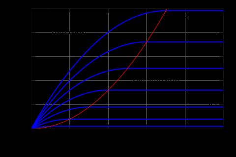
42 Diodes 1N4148 diode If a diode is subject to more voltage or current than it can handle, expect it to heat up (or worse; melt, smoke, ). Some diodes are well-suited to high currents 1A or more others like the 1N4148 small-signal diode shown above may only be suited for around 200mA.
 LEDs are a")

43 Light-emitting Diodes (LEDs) LEDs are a particular type of diode that convert electrical energy into light.
44 Light-emitting Diodes (LEDs) current Cathode (-) Anode (+)


45 Light-emitting Diodes (LEDs) The brightness of an LED is directly dependent on how much current it draws. The super bright LEDs drain batteries more quickly, because the extra brightness comes from the extra power being used. it s important to limit the amount of current flowing across the LED, otherwise it will burn. Use current limiting resistor.

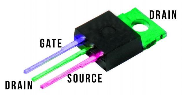
46 Light-emitting Diodes (LEDs) The first row in the table indicates how much current your LED will be able to handle continuously. In this case, you can give it 20mA or less, and it will shine its brightest at 20mA. The second row tells us what the maximum peak current should be for short bursts. This LED can handle short bumps to 30mA, but you don t want to sustain that current for too long. The first row tells us what the forward voltage drop across the LED will be. This number will help you decide how much voltage your circuit will need to supply to the LED. If you have more than one LED connected to a single power source, the forward voltage of all of the LEDs added together can t exceed the supply voltage

47 Zener Diodes Zener diodes are a special kind of diode which permits current to flow in the forward direction. What makes them different from other diodes is that Zener diodes will also allow current to flow in the reverse direction when the voltage is above a certain value. This breakdown voltage is known as the Zener voltage.
48 Diode application
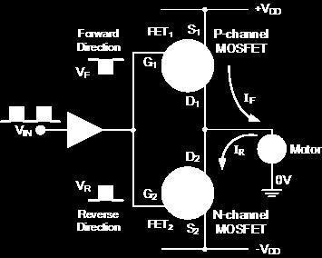
49 Transistors An electronic device which can be used as a Switch Amplifier Major Types Bipolar Junction Transistors (BJT) Metal Oxide Semiconductor Field Effect Transistors (MOSFET)
50 Transistors Bipolar Junction Transistor npn or pnp Small input base current leads to large current between emitter and collector. Major Types nmos or pmos Voltage applied to base controls current between source and drain.

51 Transistors Bipolar Junction Transistor
52 Transistors
53 Transistors
54 Transistor as switch The transistor needs a certain voltage (0.6V to 0.7V) to turn ON. Current limiting resistor Don t forget to add this resistor! The base resistor needs to be large enough to effectively limit the current, but small enough to feed the base enough current. 1mA to 10mA will usually be enough, but check your transistor s datasheet to make sure. Here we use an NPN to control an LED
55 Transistor as switch Here we use an PNP to control motor
56 Transistors as Amplifier One quirk of the common emitter, though, is that it inverts the input signal
57 Transistor as Amplifier The Darlington pair is a great tool if you need to drive a large (current hungry ) load with a very small input current.
58 Transistors - MOSFET Operation similar to a BJT
 V OUT = V DS = V DD = 1 MOSFET operates as an open switch Gate-source voltage is much greater than")
 Min channel resistance R DS(on) < 0.1Ω V OUT = V DS = 0.")
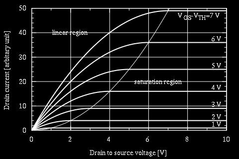
59 Transistors - MOSFET Gate-source voltage less than threshold voltage V GS < V TH MOSFET is OFF ( Cut-off region ) No Drain current flows ( I D = 0 ) V OUT = V DS = V DD = 1 MOSFET operates as an open switch Gate-source voltage is much greater than threshold voltage V GS > V TH MOSFET is ON ( saturation region ) Max Drain current flows ( I D = V DD / R L ) V DS = 0V (ideal saturation) Min channel resistance R DS(on) < 0.1Ω V OUT = V DS = 0.2V due to R DS(on) MOSFET operates as a low resistance closed switch
60 Transistors - MOSFET
61 Power MOSFET A power MOSFET is a specific type of metal oxide semiconductor field-effect transistor (MOSFET) designed to handle significant power levels. The power MOSFET is the most widely used low-voltage (that is, less than 200 V) switch. It can be found in most power supplies, DC to DC converters, and low voltage motor controllers.

62 Power MOSFET IRFD120
63 BJT vs MOSFET Unlike bipolar transistors, MOSFET is voltage controlled. While BJT is current controlled, the base resistor needs to be carefully calculated according to the amount of current being switched. Not so with a MOSFET. Just apply enough voltage to the gate and the switch operates. Because they are voltage controlled, MOSFET have a very high input impedance, so just about anything can drive them. MOSFET has high input impedance.
64 Skills
65 Skills Troubleshooting steps: Recheck connections Check voltage using DMM Breakdown the circuit and make sure every part is doing what it is supposed to do You can use power supplies to simulate signal inputs from other parts in the circuit Try to change one thing at a time
66 Skills Example. You made the following circuit but it is not working: Motor Driving circuit
67 Skills Example. You made the following circuit but it is not working: Motor Driving circuit
68 Skills Example. You made the following circuit but it is not working: Motor Driving circuit
69 Skills Example. You made the following circuit but it is not working: Same voltage Motor Driving circuit
70 Skills Example. You made the following circuit but it is not working: Motor Driving circuit Both working?
71 Skills Example. You made the following circuit but it is not working: Motor Driving circuit No Yes Both working?
72 Skills Example. You made the following circuit but it is not working: Motor Driving circuit troubleshoot

73 Skills Example. You made the following circuit but it is not working: Motor Driving circuit Yes Yes Both working?
74 Skills Example. You made the following circuit but it is not working: Motor Driving circuit Not working?


75 Skills Example. You made the following circuit but it is not working: Different than
76 Skills Common errors: Power not connected or turned ON Always check your source Circuit wiring Break the circuits into parts, and debug it using DMMs and power supplies Common ground Ground is an imaginary reference point All circuit parts should share a common ground All power supplies should also share that same common ground
77 Skills Common errors: Components are burnt out ICs and transistors can be burnt out and not working Based on what is not working in the circuit, you can guess which part might be burnt out There are IC testers to test you IC Also try exchanging the IC or transistor and see if the circuit work
78 Skills Common errors: Using components incorrectly If the IC passes, but circuit is still not working, then you might simply be using your IC incorrectly Check the datasheet Loose connections You know you have a loose connection when the circuit sometimes works and sometimes doesn t
79 Skills Common errors: Current issues Usually happens when independent parts work, but don t work when integrated Power supplies usually give you as much current as you need Use them to simulate signal inputs from other parts in the circuit If it works, then current issue confirmed Use the signal to control a switching circuit that powers your next part Use amplifier/more efficient transistors to supply more current within the circuit
80 Skills Example. You made the following circuit but it is not working:
81 Skills Example. You made the following circuit but it is not working:
82 Skills Example. You made the following circuit but it is not working: correct
83 Skills Example. You made the following circuit but it is not working: correct
84 Skills Example. You made the following circuit but it is not working: Wrong!
85 Skills Example. You made the following circuit but it is not working: This could be burnt
86 Skills Example. You made the following circuit but it is not working: Connections might be wrong
87 Skills Example. You made the following circuit but it is not working: Current might not be enough
88 Skills Example. You made the following circuit but it is not working: etc...
89 References
Experiment 6: Biasing Circuitry
 1 Objective UNIVERSITY OF CALIFORNIA AT BERKELEY College of Engineering Department of Electrical Engineering and Computer Sciences EE105 Lab Experiments Experiment 6: Biasing Circuitry Setting up a biasing
Field Effect Transistors
 Field Effect Transistors Purpose In this experiment we introduce field effect transistors (FETs). We will measure the output characteristics of a FET, and then construct a common-source amplifier stage,
Experiment 6: Biasing Circuitry
 1 Objective UNIVERSITY OF CALIFORNIA AT BERKELEY College of Engineering Department of Electrical Engineering and Computer Sciences EE105 Lab Experiments Experiment 6: Biasing Circuitry Setting up a biasing
EXPERIMENT 5 CURRENT AND VOLTAGE CHARACTERISTICS OF BJT
 EXPERIMENT 5 CURRENT AND VOLTAGE CHARACTERISTICS OF BJT 1. OBJECTIVES 1.1 To practice how to test NPN and PNP transistors using multimeter. 1.2 To demonstrate the relationship between collector current
Concepts to be Covered
 Introductory Medical Device Prototyping Analog Circuits Part 2 Semiconductors, http://saliterman.umn.edu/ Department of Biomedical Engineering, University of Minnesota Concepts to be Covered Semiconductors
4 Transistors. 4.1 IV Relations
 4 Transistors Due date: Sunday, September 19 (midnight) Reading (Bipolar transistors): HH sections 2.01-2.07, (pgs. 62 77) Reading (Field effect transistors) : HH sections 3.01-3.03, 3.11-3.12 (pgs. 113
Analog Electronic Circuits Lab-manual
 2014 Analog Electronic Circuits Lab-manual Prof. Dr Tahir Izhar University of Engineering & Technology LAHORE 1/09/2014 Contents Experiment-1:...4 Learning to use the multimeter for checking and indentifying
Physics 481 Experiment 3
 Physics 481 Experiment 3 LAST Name (print) FIRST Name (print) TRANSISTORS (BJT & FET) npn BJT n-channel MOSFET 1 Experiment 3 Transistors: BJT & FET In this experiment transistor properties and transistor
Laboratory #5 BJT Basics and MOSFET Basics
 Laboratory #5 BJT Basics and MOSFET Basics I. Objectives 1. Understand the physical structure of BJTs and MOSFETs. 2. Learn to measure I-V characteristics of BJTs and MOSFETs. II. Components and Instruments
o Semiconductor Diode Symbol: The cathode contains the N-type material and the anode contains the P-type material.
 Cornerstone Electronics Technology and Robotics I Week 16 Diodes and Transistor Switches Administration: o Prayer o Turn in quiz Review: o Design and wire a voltage divider that divides your +9 V voltage
USER MANUAL FOR THE LM2901 QUAD VOLTAGE COMPARATOR FUNCTIONAL MODULE
 USER MANUAL FOR THE LM2901 QUAD VOLTAGE COMPARATOR FUNCTIONAL MODULE LM2901 Quad Voltage Comparator 1 5/18/04 TABLE OF CONTENTS 1. Index of Figures....3 2. Index of Tables. 3 3. Introduction.. 4-5 4. Theory
EE 230 Lab Lab 9. Prior to Lab
 MOS transistor characteristics This week we look at some MOS transistor characteristics and circuits. Most of the measurements will be done with our usual lab equipment, but we will also use the parameter
Experiment 9- Single Stage Amplifiers with Passive Loads - MOS
 Experiment 9- Single Stage Amplifiers with Passive oads - MOS D. Yee,.T. Yeung, M. Yang, S.M. Mehta, and R.T. Howe UC Berkeley EE 105 1.0 Objective This is the second part of the single stage amplifier
ECE 310L : LAB 9. Fall 2012 (Hay)
") ECE 310L : LAB 9 PRELAB ASSIGNMENT: Read the lab assignment in its entirety. 1. For the circuit shown in Figure 3, compute a value for R1 that will result in a 1N5230B zener diode current of approximately
ECE 310L : LAB 9 PRELAB ASSIGNMENT: Read the lab assignment in its entirety. 1. For the circuit shown in Figure 3, compute a value for R1 that will result in a 1N5230B zener diode current of approximately
EE 330 Laboratory 8 Discrete Semiconductor Amplifiers
 EE 330 Laboratory 8 Discrete Semiconductor Amplifiers Fall 2017 Contents Objective:... 2 Discussion:... 2 Components Needed:... 2 Part 1 Voltage Controlled Amplifier... 2 Part 2 Common Source Amplifier...
Design cycle for MEMS
 Design cycle for MEMS Design cycle for ICs IC Process Selection nmos CMOS BiCMOS ECL for logic for I/O and driver circuit for critical high speed parts of the system The Real Estate of a Wafer MOS Transistor
Experiment #8: Designing and Measuring a Common-Collector Amplifier
 SCHOOL OF ENGINEERING AND APPLIED SCIENCE DEPARTMENT OF ELECTRICAL AND COMPUTER ENGINEERING ECE 2115: ENGINEERING ELECTRONICS LABORATORY Experiment #8: Designing and Measuring a Common-Collector Amplifier
EE 330 Laboratory 8 Discrete Semiconductor Amplifiers
 EE 330 Laboratory 8 Discrete Semiconductor Amplifiers Fall 2018 Contents Objective:...2 Discussion:...2 Components Needed:...2 Part 1 Voltage Controlled Amplifier...2 Part 2 A Nonlinear Application...3
Lecture 3: Transistors
 Lecture 3: Transistors Now that we know about diodes, let s put two of them together, as follows: collector base emitter n p n moderately doped lightly doped, and very thin heavily doped At first glance,
the reactance of the capacitor, 1/2πfC, is equal to the resistance at a frequency of 4 to 5 khz.
 EXPERIMENT 12 INTRODUCTION TO PSPICE AND AC VOLTAGE DIVIDERS OBJECTIVE To gain familiarity with PSPICE, and to review in greater detail the ac voltage dividers studied in Experiment 14. PROCEDURE 1) Connect
Introduction to Lab Equipment and Components
 331: nalog lectronics University of Toronto 2017 Lab 0: ntroduction to Lab quipment and omponents ntroduction The first part of this lab introduces you to the lab equipment and components you will use
Lab 1 - Revisited. Oscilloscope demo IAP Lecture 2 1
 Lab 1 - Revisited Display signals on scope Measure the time, frequency, voltage visually and with the scope Voltage measurement* Build simple circuits on a protoboard.* Oscilloscope demo 6.091 IAP Lecture
University of Jordan School of Engineering Electrical Engineering Department. EE 204 Electrical Engineering Lab
 University of Jordan School of Engineering Electrical Engineering Department EE 204 Electrical Engineering Lab EXPERIMENT 1 MEASUREMENT DEVICES Prepared by: Prof. Mohammed Hawa EXPERIMENT 1 MEASUREMENT
Semiconductor analyser AS4002P User Manual
 Semiconductor analyser AS4002P User Manual Copyright Ormelabs (C) 2010 http://www.ormelabs.com 1 CONTENTS SECTION Page SECTION 1: Introduction... 3 SECTION 2: Features... 3 SECTION 3: Component analysis...
Analog and Telecommunication Electronics
 Politecnico di Torino - ICT School Analog and Telecommunication Electronics F2 Active power devices»mos»bjt» IGBT, TRIAC» Safe Operating Area» Thermal analysis 30/05/2012-1 ATLCE - F2-2011 DDC Lesson F2:
LAB 1 AN EXAMPLE MECHATRONIC SYSTEM: THE FURBY
 LAB 1 AN EXAMPLE MECHATRONIC SYSTEM: THE FURBY Objectives Preparation Tools To see the inner workings of a commercial mechatronic system and to construct a simple manual motor speed controller and current
BME 3512 Bioelectronics Laboratory Five - Operational Amplifiers
 BME 351 Bioelectronics Laboratory Five - Operational Amplifiers Learning Objectives: Be familiar with the operation of a basic op-amp circuit. Be familiar with the characteristics of both ideal and real
Sonoma State University Department of Engineering Science Fall 2017
 ES-110 Laboratory Introduction to Engineering & Laboratory Experience Saeid Rahimi, Ph.D. Lab 7 Introduction to Transistors Introduction As we mentioned before, diodes have many applications which are
Device Technologies. Yau - 1
 Device Technologies Yau - 1 Objectives After studying the material in this chapter, you will be able to: 1. Identify differences between analog and digital devices and passive and active components. Explain
Dr. Charles Kim ELECTRONICS I. Lab 6 Bipolar Junction Transistor (BJT) II TRADITIONAL LAB
 II TRADITIONAL LAB") ELECTRONICS I Lab 6 Bipolar Junction Transistor (BJT) II TRADITIONAL LAB MOBILE STUDIO LAB Before We Start As the title of this lab says, this lab is about designing a Common-Emitter Amplifier, and this
ELECTRONICS I Lab 6 Bipolar Junction Transistor (BJT) II TRADITIONAL LAB MOBILE STUDIO LAB Before We Start As the title of this lab says, this lab is about designing a Common-Emitter Amplifier, and this
Applications of diodes
 Applications of diodes Learners should be able to: (a) describe the I V characteristics of a silicon diode (b) describe the use of diodes for component protection in DC circuits and half-wave rectification
9 Feedback and Control
 9 Feedback and Control Due date: Tuesday, October 20 (midnight) Reading: none An important application of analog electronics, particularly in physics research, is the servomechanical control system. Here
// Parts of a Multimeter
 Using a Multimeter // Parts of a Multimeter Often you will have to use a multimeter for troubleshooting a circuit, testing components, materials or the occasional worksheet. This section will cover how
Electronics EECE2412 Spring 2017 Exam #2
 Electronics EECE2412 Spring 2017 Exam #2 Prof. Charles A. DiMarzio Department of Electrical and Computer Engineering Northeastern University 30 March 2017 File:12198/exams/exam2 Name: : General Rules:
Digital Logic Troubleshooting
 Digital Logic Troubleshooting Troubleshooting Basic Equipment Circuit diagram Data book (for IC pin outs) Logic probe Voltmeter Oscilloscope Advanced Logic analyzer 1 Basic ideas Troubleshooting is systemic
EE 320 L LABORATORY 9: MOSFET TRANSISTOR CHARACTERIZATIONS. by Ming Zhu UNIVERSITY OF NEVADA, LAS VEGAS 1. OBJECTIVE 2. COMPONENTS & EQUIPMENT
 EE 320 L ELECTRONICS I LABORATORY 9: MOSFET TRANSISTOR CHARACTERIZATIONS by Ming Zhu DEPARTMENT OF ELECTRICAL AND COMPUTER ENGINEERING UNIVERSITY OF NEVADA, LAS VEGAS 1. OBJECTIVE Get familiar with MOSFETs,
Semiconductors, ICs and Digital Fundamentals
 Semiconductors, ICs and Digital Fundamentals The Diode The semiconductor phenomena. Diode performance with ac and dc currents. Diode types: General purpose LED Zener The Diode The semiconductor phenomena
BJT Characteristics & Common Emitter Transistor Amplifier
 LAB #07 Objectives 1. To graph the collector characteristics of a transistor. 2. To measure AC and DC voltages in a common-emitter amplifier. Theory BJT A bipolar (junction) transistor (BJT) is a three-terminal
Experiment No. 9 DESIGN AND CHARACTERISTICS OF COMMON BASE AND COMMON COLLECTOR AMPLIFIERS
 Experiment No. 9 DESIGN AND CHARACTERISTICS OF COMMON BASE AND COMMON COLLECTOR AMPLIFIERS 1. Objective: The objective of this experiment is to explore the basic applications of the bipolar junction transistor
L MOSFETS, IDENTIFICATION, CURVES. PAGE 1. I. Review of JFET (DRAW symbol for n-channel type, with grounded source)
") L.107.4 MOSFETS, IDENTIFICATION, CURVES. PAGE 1 I. Review of JFET (DRAW symbol for n-channel type, with grounded source) 1. "normally on" device A. current from source to drain when V G = 0 no need to
L.107.4 MOSFETS, IDENTIFICATION, CURVES. PAGE 1 I. Review of JFET (DRAW symbol for n-channel type, with grounded source) 1. "normally on" device A. current from source to drain when V G = 0 no need to
Analog Circuits Part 2 Semiconductors
 Introductory Medical Device Prototyping Analog Circuits Part 2 Semiconductors, http://saliterman.umn.edu/ Department of Biomedical Engineering, University of Minnesota Concepts to be Covered Semiconductors
Electronics. RC Filter, DC Supply, and 555
 Electronics RC Filter, DC Supply, and 555 0.1 Lab Ticket Each individual will write up his or her own Lab Report for this two-week experiment. You must also submit Lab Tickets individually. You are expected
ITT Technical Institute. ET215 Devices 1. Unit 6 Chapter 3, Sections
 ITT Technical Institute ET215 Devices 1 Unit 6 Chapter 3, Sections 3.7-3.9 Chapter 3 Section 3.7 The Bipolar Transistor as a Switch Objectives: Explain how a transistor can be used as a switch 1. Compute
Lab 2: Discrete BJT Op-Amps (Part I)
") Lab 2: Discrete BJT Op-Amps (Part I) This is a three-week laboratory. You are required to write only one lab report for all parts of this experiment. 1.0. INTRODUCTION In this lab, we will introduce and
Lab 2: Discrete BJT Op-Amps (Part I) This is a three-week laboratory. You are required to write only one lab report for all parts of this experiment. 1.0. INTRODUCTION In this lab, we will introduce and
COLLECTOR DRAIN BASE GATE EMITTER. Applying a voltage to the Gate connection allows current to flow between the Drain and Source connections.
 MOSFETS Although the base current in a transistor is usually small (< 0.1 ma), some input devices (e.g. a crystal microphone) may be limited in their output. In order to overcome this, a Field Effect Transistor
INTERNATIONAL JOURNAL OF ELECTRONICS AND COMMUNICATION ENGINEERING & TECHNOLOGY (IJECET)
") INTERNATIONAL JOURNAL OF ELECTRONICS AND COMMUNICATION ENGINEERING & TECHNOLOGY (IJECET) International Journal of Electronics and Communication Engineering & Technology (IJECET), ISSN 0976 ISSN 0976 6464(Print)
INTERNATIONAL JOURNAL OF ELECTRONICS AND COMMUNICATION ENGINEERING & TECHNOLOGY (IJECET) International Journal of Electronics and Communication Engineering & Technology (IJECET), ISSN 0976 ISSN 0976 6464(Print)
Lab no. 4 Bipolar Transistor (NPN and PNP)
") Lab no. 4 Bipolar Transistor (NPN and PNP) Transistors are semiconductor devices that enable to control the flow of large current by much smaller current. Bipolar transistor consists of three areas of
Lab no. 4 Bipolar Transistor (NPN and PNP) Transistors are semiconductor devices that enable to control the flow of large current by much smaller current. Bipolar transistor consists of three areas of
Physics 364, Fall 2012, reading due your answers to by 11pm on Thursday
 Physics 364, Fall 2012, reading due 2012-10-25. Email your answers to ashmansk@hep.upenn.edu by 11pm on Thursday Course materials and schedule are at http://positron.hep.upenn.edu/p364 Assignment: (a)
4.2.2 Metal Oxide Semiconductor Field Effect Transistor (MOSFET)
") 4.2.2 Metal Oxide Semiconductor Field Effect Transistor (MOSFET) The Metal Oxide Semitonductor Field Effect Transistor (MOSFET) has two modes of operation, the depletion mode, and the enhancement mode.
4.2.2 Metal Oxide Semiconductor Field Effect Transistor (MOSFET) The Metal Oxide Semitonductor Field Effect Transistor (MOSFET) has two modes of operation, the depletion mode, and the enhancement mode.
BJT Amplifier. Superposition principle (linear amplifier)
") BJT Amplifier Two types analysis DC analysis Applied DC voltage source AC analysis Time varying signal source Superposition principle (linear amplifier) The response of a linear amplifier circuit excited
BJT Amplifier Two types analysis DC analysis Applied DC voltage source AC analysis Time varying signal source Superposition principle (linear amplifier) The response of a linear amplifier circuit excited
= V IN. and V CE. = the supply voltage 0.7 V, the transistor is on, V BE. = 0.7 V and V CE. until saturation is reached.
 Switching Circuits Learners should be able to: (a) describe and analyse the operation and use of n-channel enhancement mode MOSFETs and npn transistors in switching circuits, including those which interface
Unit III FET and its Applications. 2 Marks Questions and Answers
 Unit III FET and its Applications 2 Marks Questions and Answers 1. Why do you call FET as field effect transistor? The name field effect is derived from the fact that the current is controlled by an electric
Multi-Transistor Configurations
 Experiment-3 Multi-Transistor Configurations Introduction Comment The objectives of this experiment are to examine the operating characteristics of several of the most common multi-transistor configurations,
Analog Electronics. Electronic Devices, 9th edition Thomas L. Floyd Pearson Education. Upper Saddle River, NJ, All rights reserved.
 Analog Electronics BJT Structure The BJT has three regions called the emitter, base, and collector. Between the regions are junctions as indicated. The base is a thin lightly doped region compared to the
5.1 BJT Device Structure and Physical Operation
 11/28/2004 section 5_1 BJT Device Structure and Physical Operation blank 1/2 5.1 BJT Device Structure and Physical Operation Reading Assignment: pp. 377-392 Another kind of transistor is the Bipolar Junction
Experiment # 4: BJT Characteristics and Applications
 ENGR 301 Electrical Measurements Experiment # 4: BJT Characteristics and Applications Objective: To characterize a bipolar junction transistor (BJT). To investigate basic BJT amplifiers and current sources.
Physics 309 Lab 3 Bipolar junction transistor
 Physics 39 Lab 3 Bipolar junction transistor The purpose of this third lab is to learn the principles of operation of a bipolar junction transistor, how to characterize its performances, and how to use
555 Morse Code Practice Oscillator Kit (draft 1.1)
") This kit was designed to be assembled in about 30 minutes and accomplish the following learning goals: 1. Learn to associate schematic symbols with actual electronic components; 2. Provide a little experience
This kit was designed to be assembled in about 30 minutes and accomplish the following learning goals: 1. Learn to associate schematic symbols with actual electronic components; 2. Provide a little experience
I E I C since I B is very small
 Figure 2: Symbols and nomenclature of a (a) npn and (b) pnp transistor. The BJT consists of three regions, emitter, base, and collector. The emitter and collector are usually of one type of doping, while
Data Conversion and Lab Lab 3 Spring Analog to Digital Converter
 Analog to Digital Converter Lab Report Objectives See separate report form located on the course webpage. This form should be completed during the performance of this lab. 1) To construct and operate an
Mechatronics and Measurement. Lecturer:Dung-An Wang Lecture 2
 Mechatronics and Measurement Lecturer:Dung-An Wang Lecture 2 Lecture outline Reading:Ch3 of text Today s lecture Semiconductor 2 Diode 3 4 Zener diode Voltage-regulator diodes. This family of diodes exhibits
Technological Studies. - Applied Electronics (H) TECHNOLOGICAL STUDIES HIGHER APPLIED ELECTRONICS. Transistors. Craigmount High School 1
 TECHNOLOGICAL STUDIES HIGHER APPLIED ELECTRONICS. Transistors. Craigmount High School 1") TECHNOLOGICAL STUDIES HIGHER APPLIED ELECTRONICS Transistors Craigmount High School 1 APPLIED ELECTRONICS Outcome 1 - Design and construct electronic systems to meet given specifications When you have
TECHNOLOGICAL STUDIES HIGHER APPLIED ELECTRONICS Transistors Craigmount High School 1 APPLIED ELECTRONICS Outcome 1 - Design and construct electronic systems to meet given specifications When you have
LABORATORY 3 v3 CIRCUIT ELEMENTS
 University of California Berkeley Department of Electrical Engineering and Computer Sciences EECS 100, Professor Leon Chua LABORATORY 3 v3 CIRCUIT ELEMENTS The purpose of this laboratory is to familiarize
Electronic Component Applications
 Western Technical College 10660124 Electronic Component Applications Course Outcome Summary Course Information Description Career Cluster Instructional Level Total Credits 2.00 Total Hours 60.00 Solid
Practical 2P12 Semiconductor Devices
 Practical 2P12 Semiconductor Devices What you should learn from this practical Science This practical illustrates some points from the lecture courses on Semiconductor Materials and Semiconductor Devices
Intelligent Semiconductor Analyzer User Manual
 Intelligent Semiconductor Analyzer User Manual Please read this manual before switching the unit on. Important safety information inside. 2 Contents Page 1.Introduction... 4 2.Important Considerations...
PHYS 3152 Methods of Experimental Physics I E2. Diodes and Transistors 1
 Part I Diodes Purpose PHYS 3152 Methods of Experimental Physics I E2. In this experiment, you will investigate the current-voltage characteristic of a semiconductor diode and examine the applications of
BME/ISE 3512 Bioelectronics. Laboratory Five - Operational Amplifiers
 BME/ISE 3512 Bioelectronics Laboratory Five - Operational Amplifiers Learning Objectives: Be familiar with the operation of a basic op-amp circuit. Be familiar with the characteristics of both ideal and
PreLab 7: LED Blinker (Due Oct 30)
") GOAL PreLab 7: LED Blinker (Due Oct 30) The overall goal of Lab 7 is to demonstrate a two-led blinker with adjustable frequency. This is a two-week lab. The first week involves designing and testing a
GOAL PreLab 7: LED Blinker (Due Oct 30) The overall goal of Lab 7 is to demonstrate a two-led blinker with adjustable frequency. This is a two-week lab. The first week involves designing and testing a
PHY405F 2009 EXPERIMENT 6 SIMPLE TRANSISTOR CIRCUITS
 PHY405F 2009 EXPERIMENT 6 SIMPLE TRANSISTOR CIRCUITS Due Date (NOTE CHANGE): Thursday, Nov 12 th @ 5 pm; Late penalty in effect! Most active electronic devices are based on the transistor as the fundamental
Operational Amplifiers
 Operational Amplifiers Reading Horowitz & Hill handout Notes, Chapter 9 Introduction and Objective In this lab we will examine op-amps. We will look at a few of their vast number of uses and also investigate
EE 110 Introduction to Engineering & Laboratory Experience Saeid Rahimi, Ph.D. Lab 6 Diodes: Half-Wave and Full-Wave Rectifiers Converting AC to DC
 EE 110 Introduction to Engineering & Laboratory Experience Saeid Rahimi, Ph.D. Lab 6 Diodes: Half-Wave and Full-Wave Rectifiers Converting C to DC The process of converting a sinusoidal C voltage to a
MTLE-6120: Advanced Electronic Properties of Materials. Semiconductor transistors for logic and memory. Reading: Kasap
 MTLE-6120: Advanced Electronic Properties of Materials 1 Semiconductor transistors for logic and memory Reading: Kasap 6.6-6.8 Vacuum tube diodes 2 Thermionic emission from cathode Electrons collected
Electronics EECE2412 Spring 2018 Exam #2
 Electronics EECE2412 Spring 2018 Exam #2 Prof. Charles A. DiMarzio Department of Electrical and Computer Engineering Northeastern University 29 March 2018 File:12262/exams/exam2 Name: General Rules: You
UNIT 3: FIELD EFFECT TRANSISTORS
 FIELD EFFECT TRANSISTOR: UNIT 3: FIELD EFFECT TRANSISTORS The field effect transistor is a semiconductor device, which depends for its operation on the control of current by an electric field. There are
Field Effect Transistors (npn)
") Field Effect Transistors (npn) gate drain source FET 3 terminal device channel e - current from source to drain controlled by the electric field generated by the gate base collector emitter BJT 3 terminal
Field Effect Transistors (npn) gate drain source FET 3 terminal device channel e - current from source to drain controlled by the electric field generated by the gate base collector emitter BJT 3 terminal
8. Characteristics of Field Effect Transistor (MOSFET)
") 1 8. Characteristics of Field Effect Transistor (MOSFET) 8.1. Objectives The purpose of this experiment is to measure input and output characteristics of n-channel and p- channel field effect transistors
1 8. Characteristics of Field Effect Transistor (MOSFET) 8.1. Objectives The purpose of this experiment is to measure input and output characteristics of n-channel and p- channel field effect transistors
Basic Fabrication Steps
 Basic Fabrication Steps and Layout Somayyeh Koohi Department of Computer Engineering Adapted with modifications from lecture notes prepared by author Outline Fabrication steps Transistor structures Transistor
Dev Bhoomi Institute Of Technology Department of Electronics and Communication Engineering PRACTICAL INSTRUCTION SHEET
 Dev Bhoomi Institute Of Technology Department of Electronics and Communication Engineering PRACTICAL INSTRUCTION SHEET LABORATORY MANUAL EXPERIMENT NO. ISSUE NO. : ISSUE DATE: REV. NO. : REV. DATE : PAGE:
The Field Effect Transistor
 FET, OPAmps I. p. 1 Field Effect Transistors and Op Amps I The Field Effect Transistor This lab begins with some experiments on a junction field effect transistor (JFET), type 2N5458, and then continues
Experiment #7: Designing and Measuring a Common-Emitter Amplifier
 SCHOOL OF ENGINEERING AND APPLIED SCIENCE DEPARTMENT OF ELECTRICAL AND COMPUTER ENGINEERING ECE 2115: ENGINEERING ELECTRONICS LABORATORY Experiment #7: Designing and Measuring a Common-Emitter Amplifier
Electronic Circuits - Tutorial 07 BJT transistor 1
 Electronic Circuits - Tutorial 07 BJT transistor 1-1 / 20 - T & F # Question 1 A bipolar junction transistor has three terminals. T 2 For operation in the linear or active region, the base-emitter junction
Transistor Characteristics
 Transistor Characteristics Topics covered in this presentation: Transistor Construction Transistor Operation Transistor Characteristics 1 of 15 The Transistor The transistor is a semiconductor device that
Learning Outcomes. Spiral 2-6. Current, Voltage, & Resistors DIODES
 26.1 26.2 Learning Outcomes Spiral 26 Semiconductor Material MOS Theory I underst why a diode conducts current under forward bias but does not under reverse bias I underst the three modes of operation
4-bit counter circa bit counter circa 1990
 Digital Logic 4-bit counter circa 1960 8-bit counter circa 1990 Logic gates Operates on logical values (TRUE = 1, FALSE = 0) NOT AND OR XOR 0-1 1-0 0 0 0 1 0 0 0 1 0 1 1 1 0 0 0 1 0 1 0 1 1 1 1 1 0 0 0
DISCUSSION The best way to test a transistor is to connect it in a circuit that uses the transistor.
 Exercise 1: EXERCISE OBJECTIVE When you have completed this exercise, you will be able to test a transistor by forward biasing and reverse biasing the junctions. You will verify your results with an ohmmeter.
Chapter 8: Field Effect Transistors
 Chapter 8: Field Effect Transistors Transistors are different from the basic electronic elements in that they have three terminals. Consequently, we need more parameters to describe their behavior than
Georgia Institute of Technology School of Electrical and Computer Engineering. Midterm Exam
 Georgia Institute of Technology School of Electrical and Computer Engineering Midterm Exam ECE-3400 Fall 2013 Tue, September 24, 2013 Duration: 80min First name Solutions Last name Solutions ID number
ELEG 309 Laboratory 4
 ELEG 309 Laboratory 4 BIPOLAR-TRANSISTOR BASICS April 17, 2000 1 Objectives Our overall objective is to familiarize you with the basic properties of Bipolar Junction Transistors (BJTs) in preparation for
Unit 3: Introduction to Op- amps and Diodes
 Unit 3: Introduction to Op- amps and Diodes Differential gain Operational amplifiers are powerful building blocks conceptually simple, easy to use, versatile, and inexpensive. A great deal of analog electronic
Solid State Devices- Part- II. Module- IV
 Solid State Devices- Part- II Module- IV MOS Capacitor Two terminal MOS device MOS = Metal- Oxide- Semiconductor MOS capacitor - the heart of the MOSFET The MOS capacitor is used to induce charge at the
ELEC 350L Electronics I Laboratory Fall 2012
 ELEC 350L Electronics I Laboratory Fall 2012 Lab #9: NMOS and CMOS Inverter Circuits Introduction The inverter, or NOT gate, is the fundamental building block of most digital devices. The circuits used
LABORATORY EXPERIMENT. Infrared Transmitter/Receiver
 LABORATORY EXPERIMENT Infrared Transmitter/Receiver (Note to Teaching Assistant: The week before this experiment is performed, place students into groups of two and assign each group a specific frequency
Chapter 3-2 Semiconductor devices Transistors and Amplifiers-BJT Department of Mechanical Engineering
 MEMS1082 Chapter 3-2 Semiconductor devices Transistors and Amplifiers-BJT Bipolar Transistor Construction npn BJT Transistor Structure npn BJT I = I + E C I B V V BE CE = V = V B C V V E E Base-to-emitter
SAMPLE FINAL EXAMINATION FALL TERM
 ENGINEERING SCIENCES 154 ELECTRONIC DEVICES AND CIRCUITS SAMPLE FINAL EXAMINATION FALL TERM 2001-2002 NAME Some Possible Solutions a. Please answer all of the questions in the spaces provided. If you need
Electronics I Circuit Drawings. Robert R. Krchnavek Rowan University Spring, 2018
 Electronics I Circuit Drawings Robert R. Krchnavek Rowan University Spring, 2018 Ideal Diode Piecewise Linear Models of a Diode Piecewise Linear Models of a Diode 1 r d Piecewise Linear Models of a Diode
Current Mirrors. Basic BJT Current Mirror. Current mirrors are basic building blocks of analog design. Figure shows the basic NPN current mirror.
 Current Mirrors Basic BJT Current Mirror Current mirrors are basic building blocks of analog design. Figure shows the basic NPN current mirror. For its analysis, we assume identical transistors and neglect
ME 4447 / 6405 Student Lecture. Transistors. Abiodun Otolorin Michael Abraham Waqas Majeed
 ME 4447 / 6405 Student Lecture Transistors Abiodun Otolorin Michael Abraham Waqas Majeed Lecture Overview Transistor? History Underlying Science Properties Types of transistors Bipolar Junction Transistors
FIELD- EFFECT TRANSISTORS: MOSFETS
 FIELD- EFFECT TRANSISTORS: MOSFETS LAB 8: INTRODUCTION TO FETS AND USING THEM AS CURRENT CONTROLLERS As discussed in the last lab, transistors are the basic devices providing control of large currents
Exercise 6-2. The IGBT EXERCISE OBJECTIVES
 Exercise 6-2 The IGBT EXERCISE OBJECTIVES At the completion of this exercise, you will know the behaviour of the IGBT during switching operation. You will be able to explain how IGBT switching can be improved.