CS/ECE 5710/6710. Composite Layout
|
|
|
- Matilda Dean
- 5 years ago
- Views:
Transcription
1 CS/ECE 5710/6710 Introduction to Layout Inverter Layout Example Layout Design Rules Composite Layout Drawing the mask layers that will be used by the fabrication folks to make the devices Very different from schematics In schematics you re describing the LOGICAL connections In layout, you re describing the PHYSICAL placement of everything! Use colored regions to define the different layers that are patterned onto the silicon 1
2 N-type Transistor D + +Vgs G S Vds - i electrons N-type from the top Top view shows patterns that make up the transistor 2

3 Diffusion Mask Mask for just the diffused regions Polysilicon Mask Mask for just the polysilicon areas 3

4 Diffusion (active) Mask Diffused (active) mask is actually drawn as a solid rectangle Polysilicon Mask Polysilicon mask goes on top of the active 4

5 Combine the two masks You get an N-type transistor There are other steps in the process P-type transistor Same type of masks as the N-type But, you have to get the substrate right and you have to dope the diffusion differently 5

 Metal for interconnect Cutaway Photo")
6 General CMOS cross section Note that the general substrate is P-type The N-substrate for the P-transistor is in a well There are lots of other layers Thick SiO 2 oxide ( field oxide ) Thin SiO 2 oxide ( gate oxide ) Metal for interconnect Cutaway Photo 6


7 A Cutaway View CMOS structure with both transistor types, and top-view structure Top View from that Section Note the different mask layers that correspond to the different transistor layers In particular, note the N-well and P-select layers 7
8 This is an Inverter In Gnd Vdd Out Layout in Cadence Each color corresponds to a mask layer Draw rectangles to describe mask regions A LOT of things to keep in mind connectivity, functionality, design rules 8
")
 Nselect, Pselect")
9 What are the layers? Metal3 Metal2 Metal1 CC, Via, Via2 Polysilicon (Poly) Nselect, Pselect Nactive, Pactive Nwell What are the layers? Metal3 Via2 Metal2 Via Metal1 CC Polysilicon (Poly) Nselect, Pselect Nactive, Pactive Nwell 9

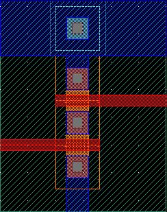
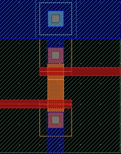
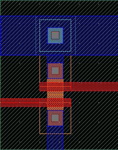
10 Photo of Interconnect Back to the Inverter Let s walk through drawing this inverter You can draw layers in whatever order makes sense to you 10
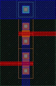
11 Layout Basics Where poly crosses active = transistor For N-type, nactive over the substrate (p substrate) For P-type, pactive inside an Nwell There s really only one active mask nselect and pselect layers define active types Our setup has separate nactive and pactive colors to help keep things straight. Layout Basics Diffusion, Poly, and metal all conduct But resistances are very different Diffusion is worst, poly isn t too bad, metal is by far the best Contact cuts are needed to connect between layers Make sure to use the right type of contact! CC for poly-m1, nactive-m1, pactive-m1 Via1 for M1-M2 Via2 for M2-M3 11


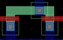
12 First Layout the Power Rails Power rail pitch is important Allows cells to connect by abutment Also add the N-well for the P-type transistor Now add Diffusion Note the M1 contacts in the diffusion Diffusion by itself will be N-type Diffusion in an N-well will be P-type Or will it? The well just defines the substrate type 12

13 Add the Select Regions Nselect defines N-type diffusion Pselect defines P-type diffusion Now add the Poly Gates Remember: crossing diffusion with Poly makes a transistor The type of the diffusion, and the type of well, define what kind of transistor 13
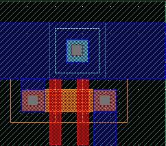
14 Note the Metal1 Connections Overlapping boxes of the same type of material make a connection Overlaps of different types of material need a contact cut of some sort Connect the Gates Connect gates together to form the inverter Note contact cuts and metal overlaps 14
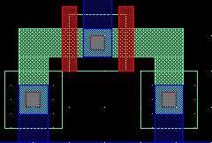
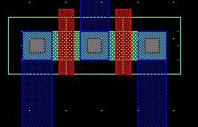
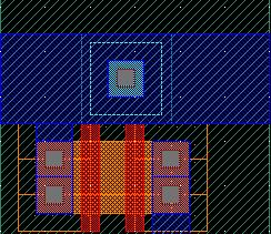
15 Layout Subtlety We currently think of transistors as threeterminal devices Gate, Source, Drain They re really four-terminal devices There s also a connection to the substrate It s important to tie the substrate to a specific voltage GND for the P-substrate VDD for the N-well Make sure PN-diodes from active to substrate and well are reverse-biased Well (or Substrate) Contacts Connect P-substrate to GND (VSS) with a little stub of P-type diffusion (remember pselect) Connect the N-well to VDD with a little stub of N-type diffusion I.e. inside the N-well, but with nselect 15
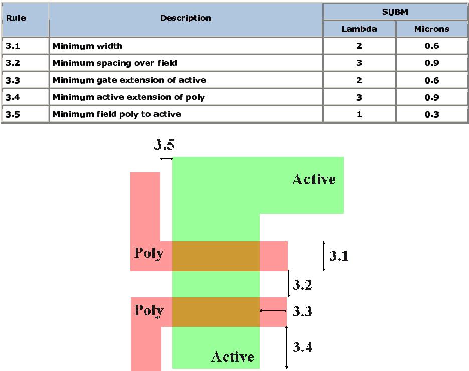
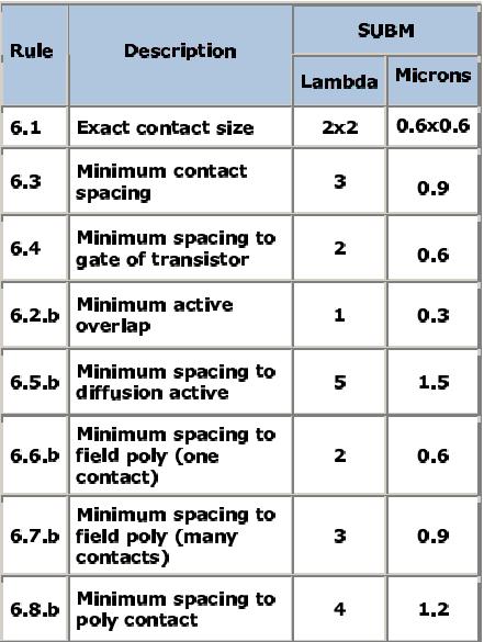
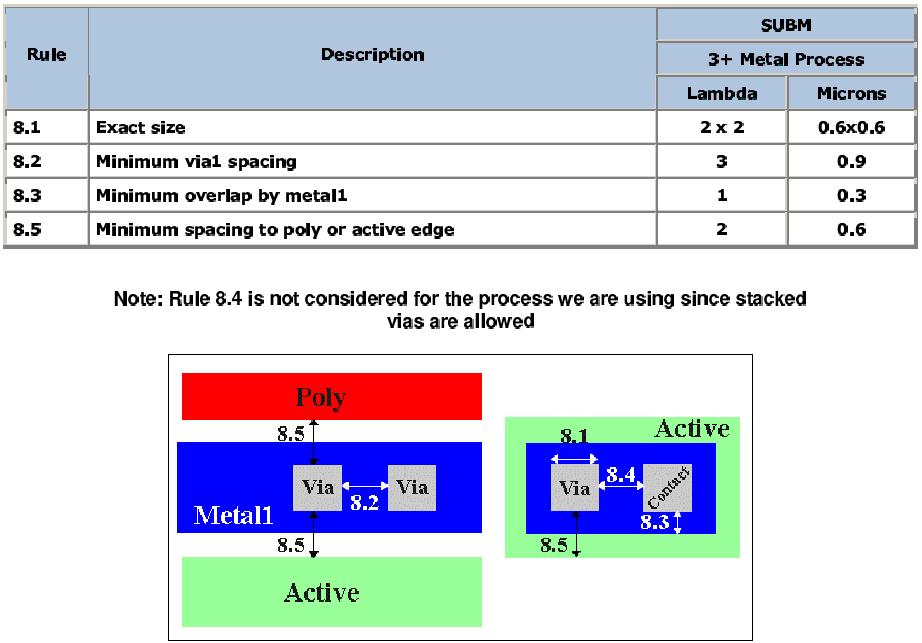
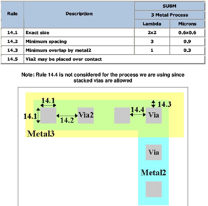
16 Layout Design Rules Define the allowed geometry of the different layers Guidelines for making safe process masks Rules about the allowed sizes and shapes of a particular layer Rules about how different layers interact Dimensions listed in one of two ways Absolute dimensions (e.g. microns or nm) Scalable dimensions in abstract units Usually called lambda Design in lambda units, then scale lambda for a particular process Intra-Layer Rules (Lambda) Same Potential Different Potential Well 12 0 or 6 18 Polysilicon 2 3 Active Select Contact or Via Hole Lambda = 0.50 => 1.0u process Lambda = 0.30 => 0.6u process 2 2 Metal1 3 3 Metal2 3 Metal

17 Intra-Layer Rules (Native) Same Potential Different Potential Well 5 0 or 5 5 Polysilicon Active Select Contact or Via Hole Dimensions are directly in microns Some things scale uniformly, others don t Native rules are generally more dense Metal Metal Metal Measurements are in microns based on scalable rules and a lambda of 0.3. Transistor Layout 17

18 Vias and Contacts Look at Inverter Layout Again Lots and lots of design rules to consider! Use Design Rule Checking (DRC) to see if everything is OK 18

19 Layout Design Rules On the class web page Modified version of the MOSIS SCMOS Rev. 8 rules Modified to show both Lambda and Micron dimensions All our design will be done in microns Because of the NCSU tech files But, even though we re using microns, we re using the SCMOS Lambda rules Print them out in color if possible! SCMOS Nwell 19

20 SCMOS Active (diffusion) SCMOS Poly 20


21 SCMOS Select SCMOS Contacts 21


22 SCMOS Contact to Poly SCMOS Contact to Active 22

23 SCMOS Metal1 SCMOS Via 23

24 SCMOS Metal2 SCMOS Via2 24


25 SCMOS Metal3 An Example: NOR NOR schematic in Composer 25
26 First Layout: Follow Schematic Note that layout of transistors follows the schematic Two P-types in series pulling up Two N-types in parallel pulling down Another Layout: Better? Same four transistors But, organized a little differently And sized a little differently 26

27 Use Shared Source/Drain Another Shared S/D 27

28 Two NOR Gates Transistor Sizing We ll get into the details later Consider a transistor s Width and Length Current capability is proportional to W/L Length is almost always minimum allowed Change width to change current capability 28
29 Sizing Rule of Thumb Also, P-type is about twice as bad as N-type Has to do with hole mobility vs. electron mobility So, make P-types twice as wide as N-types to start with Unit size for transistors this semester N-type 1.5µ (contact pitch is 1.2µ) P-type 3µ Sizing Rule of Thumb Now multiply each width by n for a series stack of n transistors. Stack of 2 in series, each transistor should be 2x unit size Stack of 3 in series, each transistor should be 3x unit size This is because series connections are like increasing the L of the device Current is proportional to W/L 29

30 For example: Notice the difference in width This roughly equalizes the current sourcing capability of pull-up and pull-down stacks in this gate 30
PHYSICAL STRUCTURE OF CMOS INTEGRATED CIRCUITS. Dr. Mohammed M. Farag
 PHYSICAL STRUCTURE OF CMOS INTEGRATED CIRCUITS Dr. Mohammed M. Farag Outline Integrated Circuit Layers MOSFETs CMOS Layers Designing FET Arrays EE 432 VLSI Modeling and Design 2 Integrated Circuit Layers
Chapter12. Chip Assembly. Figure 12.1: Starting schematic showing the three connected modules
 Chapter12 Chip Assembly Figure 12.1: Starting schematic showing the three connected modules 236 CHAPTER 12: Chip Assembly Figure 12.2: The Gen From Source dialog box 237 Figure 12.3: Initial layout before
Jack Keil Wolf Lecture. ESE 570: Digital Integrated Circuits and VLSI Fundamentals. Lecture Outline. MOSFET N-Type, P-Type.
 ESE 570: Digital Integrated Circuits and VLSI Fundamentals Jack Keil Wolf Lecture Lec 3: January 24, 2019 MOS Fabrication pt. 2: Design Rules and Layout http://www.ese.upenn.edu/about-ese/events/wolf.php
ESE 570: Digital Integrated Circuits and VLSI Fundamentals
 ESE 570: Digital Integrated Circuits and VLSI Fundamentals Lec 3: January 24, 2019 MOS Fabrication pt. 2: Design Rules and Layout Penn ESE 570 Spring 2019 Khanna Jack Keil Wolf Lecture http://www.ese.upenn.edu/about-ese/events/wolf.php
Review: CMOS Logic Gates
 Review: CMOS Logic Gates INV Schematic NOR Schematic NAND Schematic + Vsg - pmos x x Vin Vout = Vin y + Vgs - nmos CMOS inverts functions CMOS Combinational Logic x g(x,y) = x + y use DeMorgan relations
EE 330 Lecture 7. Design Rules. IC Fabrication Technology Part 1
 EE 330 Lecture 7 Design Rules IC Fabrication Technology Part 1 Review from Last Time Technology Files Provide Information About Process Process Flow (Fabrication Technology) Model Parameters Design Rules
Topic 3. CMOS Fabrication Process
 Topic 3 CMOS Fabrication Process Peter Cheung Department of Electrical & Electronic Engineering Imperial College London URL: www.ee.ic.ac.uk/pcheung/ E-mail: p.cheung@ic.ac.uk Lecture 3-1 Layout of a Inverter
EE 330 Lecture 7. Design Rules
 EE 330 Lecture 7 Design Rules Last time: Response time of logic gates A Y C L t R C HL SWn L t R C LH SWp L C L proportional to #gates driven to avg input cap of gates R SW proportional length/width Last
! Review: MOS IV Curves and Switch Model. ! MOS Device Layout. ! Inverter Layout. ! Gate Layout and Stick Diagrams. ! Design Rules. !
 ESE 570: Digital Integrated Circuits and VLSI Fundamentals Lec 3: January 21, 2017 MOS Fabrication pt. 2: Design Rules and Layout Lecture Outline! Review: MOS IV Curves and Switch Model! MOS Device Layout!
Basic Fabrication Steps
 Basic Fabrication Steps and Layout Somayyeh Koohi Department of Computer Engineering Adapted with modifications from lecture notes prepared by author Outline Fabrication steps Transistor structures Transistor
! Review: MOS IV Curves and Switch Model. ! MOS Device Layout. ! Inverter Layout. ! Gate Layout and Stick Diagrams. ! Design Rules. !
 ESE 570: Digital Integrated Circuits and VLSI Fundamentals Lec 3: January 21, 2016 MOS Fabrication pt. 2: Design Rules and Layout Lecture Outline! Review: MOS IV Curves and Switch Model! MOS Device Layout!
ESE 570: Digital Integrated Circuits and VLSI Fundamentals
 ESE 570: Digital Integrated Circuits and VLSI Fundamentals Lec 3: January 21, 2016 MOS Fabrication pt. 2: Design Rules and Layout Penn ESE 570 Spring 2016 Khanna Adapted from GATech ESE3060 Slides Lecture
Layout - Line of Diffusion. Where are we? Line of Diffusion in General. Line of Diffusion in General. Stick Diagrams. Line of Diffusion in General
 Where are we? Lots of Layout issues Line of diffusion style Power pitch it-slice pitch Routing strategies Transistor sizing Wire sizing Layout - Line of Diffusion Very common layout method Start with a
Layout of a Inverter. Topic 3. CMOS Fabrication Process. The CMOS Process - photolithography (2) The CMOS Process - photolithography (1) v o.
 The CMOS Process - photolithography (1) v o.") Layout of a Inverter Topic 3 CMOS Fabrication Process V DD Q p Peter Cheung Department of Electrical & Electronic Engineering Imperial College London v i v o Q n URL: www.ee.ic.ac.uk/pcheung/ E-mail: p.cheung@ic.ac.uk
Layout of a Inverter Topic 3 CMOS Fabrication Process V DD Q p Peter Cheung Department of Electrical & Electronic Engineering Imperial College London v i v o Q n URL: www.ee.ic.ac.uk/pcheung/ E-mail: p.cheung@ic.ac.uk
Microelectronics, BSc course
 Microelectronics, BSc course MOS circuits: CMOS circuits, construction http://www.eet.bme.hu/~poppe/miel/en/14-cmos.pptx http://www.eet.bme.hu The abstraction level of our study: SYSTEM + MODULE GATE CIRCUIT
Lecture 9: Cell Design Issues
 Lecture 9: Cell Design Issues MAH, AEN EE271 Lecture 9 1 Overview Reading W&E 6.3 to 6.3.6 - FPGA, Gate Array, and Std Cell design W&E 5.3 - Cell design Introduction This lecture will look at some of the
problem grade total
 Fall 2005 6.012 Microelectronic Devices and Circuits Prof. J. A. del Alamo Name: Recitation: November 16, 2005 Quiz #2 problem grade 1 2 3 4 total General guidelines (please read carefully before starting):
INTRODUCTION TO MOS TECHNOLOGY
 INTRODUCTION TO MOS TECHNOLOGY 1. The MOS transistor The most basic element in the design of a large scale integrated circuit is the transistor. For the processes we will discuss, the type of transistor
Introduction to CMOS VLSI Design (E158) Lecture 9: Cell Design
 Lecture 9: Cell Design") Harris Introduction to CMOS VLSI Design (E158) Lecture 9: Cell Design David Harris Harvey Mudd College David_Harris@hmc.edu Based on EE271 developed by Mark Horowitz, Stanford University MAH E158 Lecture
Harris Introduction to CMOS VLSI Design (E158) Lecture 9: Cell Design David Harris Harvey Mudd College David_Harris@hmc.edu Based on EE271 developed by Mark Horowitz, Stanford University MAH E158 Lecture
2. (2 pts) What is the major reason static CMOS NAND gates are often preferred over static CMOS NOR gates?
 What is the major reason static CMOS NAND gates are often preferred over static CMOS NOR gates?") EE 330 Final Exam Spring 05 Name Instructions: Students may bring 3 pages of notes (3 front + 3 back) to this exam. There are 0 questions and 8 problems. There are two points allocated to each question.
EE 330 Final Exam Spring 05 Name Instructions: Students may bring 3 pages of notes (3 front + 3 back) to this exam. There are 0 questions and 8 problems. There are two points allocated to each question.
MOSFETS: Gain & non-linearity
 MOFET: ain & non-linearity source gate Polysilicon wire Heavily doped (n-type or p-type) diffusions W Inter-layer io 2 insulation Very thin (
Field-Effect Transistor (FET) is one of the two major transistors; FET derives its name from its working mechanism;
 is one of the two major transistors; FET derives its name from its working mechanism;") Chapter 3 Field-Effect Transistors (FETs) 3.1 Introduction Field-Effect Transistor (FET) is one of the two major transistors; FET derives its name from its working mechanism; The concept has been known
Chapter 3 Field-Effect Transistors (FETs) 3.1 Introduction Field-Effect Transistor (FET) is one of the two major transistors; FET derives its name from its working mechanism; The concept has been known
2.8 - CMOS TECHNOLOGY
 CMOS Technology (6/7/00) Page 1 2.8 - CMOS TECHNOLOGY INTRODUCTION Objective The objective of this presentation is: 1.) Illustrate the fabrication sequence for a typical MOS transistor 2.) Show the physical
ECE 5745 Complex Digital ASIC Design Topic 2: CMOS Devices
 ECE 5745 Complex Digital ASIC Design Topic 2: CMOS Devices Christopher Batten School of Electrical and Computer Engineering Cornell University http://www.csl.cornell.edu/courses/ece5950 Simple Transistor
Design Rules, Technology File, DRC / LVS
 Design Rules, Technology File, DRC / LVS Prof. Dr. Peter Fischer VLSI Design: Design Rules P. Fischer, TI, Uni Mannheim, Seite 1 DESIGN RULES Rules in one Layer Caused by manufacturing limits (lithography,
Sticks Diagram & Layout. Part II
 Sticks Diagram & Layout Part II Well and Substrate Taps Substrate must be tied to GND and n-well to V DD Metal to lightly-doped semiconductor forms poor connection called Shottky Diode Use heavily doped
HW#3 Solution. Dr. Parker. Spring 2014
 HW#3 olution r. Parker pring 2014 Assume for the problems below that V dd = 1.8 V, V tp0 is -.7 V. and V tn0 is.7 V. V tpbodyeffect is -.9 V. and V tnbodyeffect is.9 V. Assume ß n (k n )= 219.4 W/L µ A(microamps)/V
ESE370: Circuit-Level Modeling, Design, and Optimization for Digital Systems. Today. Variation. Variation. Process Corners.
 ESE370: Circuit-Level Modeling, Design, and Optimization for Digital Systems Day 13: October 3, 2012 Layout and Area Today Coping with Variation (from last time) Layout Transistors Gates Design rules Standard
CMOS Digital Integrated Circuits Lec 2 Fabrication of MOSFETs
 CMOS Digital Integrated Circuits Lec 2 Fabrication of MOSFETs 1 CMOS Digital Integrated Circuits 3 rd Edition Categories of Materials Materials can be categorized into three main groups regarding their
Depletion-mode operation ( 공핍형 ): Using an input gate voltage to effectively decrease the channel size of an FET
: Using an input gate voltage to effectively decrease the channel size of an FET") Ch. 13 MOSFET Metal-Oxide-Semiconductor Field-Effect Transistor : I D D-mode E-mode V g The gate oxide is made of dielectric SiO 2 with e = 3.9 Depletion-mode operation ( 공핍형 ): Using an input gate voltage
Ch. 13 MOSFET Metal-Oxide-Semiconductor Field-Effect Transistor : I D D-mode E-mode V g The gate oxide is made of dielectric SiO 2 with e = 3.9 Depletion-mode operation ( 공핍형 ): Using an input gate voltage
Chapter 3 CMOS processing technology (II)
") Chapter 3 CMOS processing technology (II) Twin-tub CMOS process 1. Provide separate optimization of the n-type and p-type transistors 2. Make it possible to optimize "Vt", "Body effect", and the "Gain"
Chapter 3 CMOS processing technology (II) Twin-tub CMOS process 1. Provide separate optimization of the n-type and p-type transistors 2. Make it possible to optimize "Vt", "Body effect", and the "Gain"
! MOS Device Layout. ! Inverter Layout. ! Gate Layout and Stick Diagrams. ! Design Rules. ! Standard Cells. ! CMOS Process Enhancements
 EE 570: igital Integrated Circuits and VLI Fundamentals Lec 3: January 18, 2018 MO Fabrication pt. 2: esign Rules and Layout Lecture Outline! MO evice Layout! Inverter Layout! Gate Layout and tick iagrams!
EE4800 CMOS Digital IC Design & Analysis. Lecture 1 Introduction Zhuo Feng
 EE4800 CMOS Digital IC Design & Analysis Lecture 1 Introduction Zhuo Feng 1.1 Prof. Zhuo Feng Office: EERC 730 Phone: 487-3116 Email: zhuofeng@mtu.edu Class Website http://www.ece.mtu.edu/~zhuofeng/ee4800fall2010.html
ECE Digital VLSI Design Course Syllabus Fall 2017
 ECE484-001 Digital VLSI Design Course Syllabus Fall 2017 Instructor: Dr. George L. Engel Phone: (618) 650-2806 Office: Email: URLs: Engineering Building Room EB3043 gengel@siue.edu http://www.siue.edu/~gengel
UNIT III VLSI CIRCUIT DESIGN PROCESSES. In this chapter we will be studying how to get the schematic into stick diagrams or layouts.
 UNIT III VLSI CIRCUIT DESIGN PROCESSES In this chapter we will be studying how to get the schematic into stick diagrams or layouts. MOS circuits are formed on four basic layers: N-diffusion P-diffusion
DIGITAL VLSI LAB ASSIGNMENT 1
 DIGITAL VLSI LAB ASSIGNMENT 1 Problem 1: NMOS and PMOS plots using Cadence. In this exercise, you are required to generate both NMOS and PMOS I-V device characteristics (I/P and O/P) using Cadence (Use
FABRICATION OF CMOS INTEGRATED CIRCUITS. Dr. Mohammed M. Farag
 FABRICATION OF CMOS INTEGRATED CIRCUITS Dr. Mohammed M. Farag Outline Overview of CMOS Fabrication Processes The CMOS Fabrication Process Flow Design Rules Reference: Uyemura, John P. "Introduction to
Lecture 0: Introduction
 Lecture 0: Introduction Introduction Integrated circuits: many transistors on one chip. Very Large Scale Integration (VLSI): bucketloads! Complementary Metal Oxide Semiconductor Fast, cheap, low power
420 Intro to VLSI Design
 Dept of Electrical and Computer Engineering 420 Intro to VLSI Design Lecture 0: Course Introduction and Overview Valencia M. Joyner Spring 2005 Getting Started Syllabus About the Instructor Labs, Problem
UNIVERSITY OF SASKATCHEWAN College of Engineering Department of Electrical Engineering. E.E VLSI Circuit Design Instructor: R.J.
 UNIVRSITY OF SASKATCHWAN College of ngineering Department of lectrical ngineering.. 432.3 VLSI Circuit Design Instructor: R.J. Bolton MID-TRM XAMINATION February 10, 2004 5:30 PM - 7:00 PM STUDNT NAM:
EE 42/100 Lecture 23: CMOS Transistors and Logic Gates. Rev A 4/15/2012 (10:39 AM) Prof. Ali M. Niknejad
 Prof. Ali M. Niknejad") A. M. Niknejad University of California, Berkeley EE 100 / 42 Lecture 23 p. 1/16 EE 42/100 Lecture 23: CMOS Transistors and Logic Gates ELECTRONICS Rev A 4/15/2012 (10:39 AM) Prof. Ali M. Niknejad University
A. M. Niknejad University of California, Berkeley EE 100 / 42 Lecture 23 p. 1/16 EE 42/100 Lecture 23: CMOS Transistors and Logic Gates ELECTRONICS Rev A 4/15/2012 (10:39 AM) Prof. Ali M. Niknejad University
+1 (479)
") Introduction to VLSI Design http://csce.uark.edu +1 (479) 575-6043 yrpeng@uark.edu Invention of the Transistor Vacuum tubes ruled in first half of 20th century Large, expensive, power-hungry, unreliable
Introduction to VLSI Design http://csce.uark.edu +1 (479) 575-6043 yrpeng@uark.edu Invention of the Transistor Vacuum tubes ruled in first half of 20th century Large, expensive, power-hungry, unreliable
Lecture 0: Introduction
 Introduction to CMOS VLSI Design Lecture : Introduction David Harris Steven Levitan Harvey Mudd College University of Pittsburgh Spring 24 Fall 28 Administrivia Professor Steven Levitan TA: Bo Zhao Syllabus
The Design and Realization of Basic nmos Digital Devices
 Proceedings of The National Conference On Undergraduate Research (NCUR) 2004 Indiana University Purdue University Indianapolis, Indiana April 15-17, 2004 The Design and Realization of Basic nmos Digital
CMOS Technology. 1. Why CMOS 2. Qualitative MOSFET model 3. Building a MOSFET 4. CMOS logic gates. Handouts: Lecture Slides. metal ndiff.
 CMOS Technology 1. Why CMOS 2. Qualitative MOSFET model 3. Building a MOSFET 4. CMOS logic gates poly pdiff metal ndiff Handouts: Lecture Slides L03 - CMOS Technology 1 Building Bits from Atoms V in V
2009 Spring CS211 Digital Systems & Lab 1 CHAPTER 3: TECHNOLOGY (PART 2)
") 1 CHAPTER 3: IMPLEMENTATION TECHNOLOGY (PART 2) Whatwillwelearninthischapter? we learn in this 2 How transistors operate and form simple switches CMOS logic gates IC technology FPGAs and other PLDs Basic
1 CHAPTER 3: IMPLEMENTATION TECHNOLOGY (PART 2) Whatwillwelearninthischapter? we learn in this 2 How transistors operate and form simple switches CMOS logic gates IC technology FPGAs and other PLDs Basic
1. (2pts) Why is the Q-point of a common source amplifier often placed near the middle of the load line?
 Why is the Q-point of a common source amplifier often placed near the middle of the load line?") EE 330 Exam 3 Fall 2014 Name Instructions: This is a 50 minute exam. Students may bring 3 page of notes (front and back) to this exam. There are 10 questions and 5 problems. There is also an optional extra
EE 330 Exam 3 Fall 2014 Name Instructions: This is a 50 minute exam. Students may bring 3 page of notes (front and back) to this exam. There are 10 questions and 5 problems. There is also an optional extra
CMOS: Fabrication principles and design rules
 CMOS: Fabrication principles and design rules João Canas Ferreira University of Porto Faculty of Engineering 2016-02-29 Topics 1 Overview of the CMOS fabrication process 2 Geometric design rules João Canas
Introduction to VLSI design using Cadence Electronic Design Automation Tools
 Bangladesh University of Engineering & Technology Department of Electrical & Electronic Engineering Introduction to VLSI design using Cadence Electronic Design Automation Tools Laboratory Module 4: Layout
Fundamentals of Integrated Circuit Design
 1. Definitions Integrated circuits Fundamentals of Integrated Circuit Design An integrated circuit (IC) is formed by components and interconnections that are fabricated on a single silicon piece of semiconductor,
Three Terminal Devices
 Three Terminal Devices - field effect transistor (FET) - bipolar junction transistor (BJT) - foundation on which modern electronics is built - active devices - devices described completely by considering
3. (2 pts) What is the approximate number of parameters in the BSIM model of a MOSFET?
 What is the approximate number of parameters in the BSIM model of a MOSFET?") EE 330 Exam 2 Fall 2017 Name Instructions: This is a 50-minute exam. Students may bring 2 pages of notes (front and back) to this exam. Each short question is worth 2 points and each problem is worth 16
EE 330 Exam 2 Fall 2017 Name Instructions: This is a 50-minute exam. Students may bring 2 pages of notes (front and back) to this exam. Each short question is worth 2 points and each problem is worth 16
Session 10: Solid State Physics MOSFET
 Session 10: Solid State Physics MOSFET 1 Outline A B C D E F G H I J 2 MOSCap MOSFET Metal-Oxide-Semiconductor Field-Effect Transistor: Al (metal) SiO2 (oxide) High k ~0.1 ~5 A SiO2 A n+ n+ p-type Si (bulk)
MOS Field Effect Transistors
 MOS Field Effect Transistors A gate contact gate interconnect n polysilicon gate source contacts W active area (thin oxide area) polysilicon gate contact metal interconnect drain contacts A bulk contact
EC0306 INTRODUCTION TO VLSI DESIGN
 EC0306 INTRODUCTION TO VLSI DESIGN UNIT I INTRODUCTION TO MOS CIRCUITS Why VLSI? Integration improves the design: o lower parasitics = higher speed; o lower power; o physically smaller. Integration reduces
EE 434 ASIC and Digital Systems. Prof. Dae Hyun Kim School of Electrical Engineering and Computer Science Washington State University.
 EE 434 ASIC and Digital Systems Prof. Dae Hyun Kim School of Electrical Engineering and Computer Science Washington State University Preliminaries VLSI Design System Specification Functional Design RTL
Transistor was first invented by William.B.Shockley, Walter Brattain and John Bardeen of Bell Labratories. In 1961, first IC was introduced.
 Unit 1 Basic MOS Technology Transistor was first invented by William.B.Shockley, Walter Brattain and John Bardeen of Bell Labratories. In 1961, first IC was introduced. Levels of Integration:- i) SSI:-
EMT 251 Introduction to IC Design
 EMT 251 Introduction to IC Design (Pengantar Rekabentuk Litar Terkamir) Semester II 2011/2012 Introduction to IC design and Transistor Fundamental Some Keywords! Very-large-scale-integration (VLSI) is
EE584 (Fall 2006) Introduction to VLSI CAD Project. Design of Ring Oscillator using NOR gates
 Introduction to VLSI CAD Project. Design of Ring Oscillator using NOR gates") EE584 (Fall 2006) Introduction to VLSI CAD Project Design of Ring Oscillator using NOR gates By, Veerandra Alluri Vijai Raghunathan Archana Jagarlamudi Gokulnaraiyn Ramaswami Instructor: Dr. Joseph Elias
EE584 (Fall 2006) Introduction to VLSI CAD Project Design of Ring Oscillator using NOR gates By, Veerandra Alluri Vijai Raghunathan Archana Jagarlamudi Gokulnaraiyn Ramaswami Instructor: Dr. Joseph Elias
Lecture #29. Moore s Law
 Lecture #29 ANNOUNCEMENTS HW#15 will be for extra credit Quiz #6 (Thursday 5/8) will include MOSFET C-V No late Projects will be accepted after Thursday 5/8 The last Coffee Hour will be held this Thursday
Unit-1. MOS Transistor Theory
 VLSI DESIGN -EEE Unit-1 MOS Transistor Theory VLSI DESIGN UNIT I Contents: 1.1 Historical Perspective 1.2 What is VLSI? - Introduction 1.3 VLSI Design Flow 1.4 Design Hierarchy 1.5 Basic MOS Transistor
1. (2pts) An SCR is formed by a stacking of alternate p and n diffused regions. How many diffused regions are needed to form a basic SCR?
 An SCR is formed by a stacking of alternate p and n diffused regions. How many diffused regions are needed to form a basic SCR?") EE 330 Practice Final Exam Spring 207 Name Instructions: Students may bring 3 pages of notes (3 front + 3 back) to this exam. There are 0 questions and 8 problems. There are two points allocated to each
EE 330 Practice Final Exam Spring 207 Name Instructions: Students may bring 3 pages of notes (3 front + 3 back) to this exam. There are 0 questions and 8 problems. There are two points allocated to each
3084 IEEE TRANSACTIONS ON NUCLEAR SCIENCE, VOL. 60, NO. 4, AUGUST 2013
 3084 IEEE TRANSACTIONS ON NUCLEAR SCIENCE, VOL. 60, NO. 4, AUGUST 2013 Dummy Gate-Assisted n-mosfet Layout for a Radiation-Tolerant Integrated Circuit Min Su Lee and Hee Chul Lee Abstract A dummy gate-assisted
Basic digital logic functions and gates
 Basic digital logic functions and gates Digital logic functions and gates are the main blocks behind digital logic design. s and 1s combine to produce values that are generated by basic gates such as NOT,
1. (2pts) What is the purpose of the buried collector in a bipolar process?
 What is the purpose of the buried collector in a bipolar process?") EE 330 Exam 2 Fall 2013 Name Instructions: This is a 50-minute exam. Students may bring 2 pages of notes (front and back) to this exam. The points allocated to each question and each problem are as indicated.
EE 330 Exam 2 Fall 2013 Name Instructions: This is a 50-minute exam. Students may bring 2 pages of notes (front and back) to this exam. The points allocated to each question and each problem are as indicated.
FUNDAMENTALS OF MODERN VLSI DEVICES
 19-13- FUNDAMENTALS OF MODERN VLSI DEVICES YUAN TAUR TAK H. MING CAMBRIDGE UNIVERSITY PRESS Physical Constants and Unit Conversions List of Symbols Preface page xi xiii xxi 1 INTRODUCTION I 1.1 Evolution
Very Large Scale Integration (VLSI)
") Very Large Scale Integration (VLSI) Lecture 6 Dr. Ahmed H. Madian Ah_madian@hotmail.com Dr. Ahmed H. Madian-VLSI 1 Contents Array subsystems Gate arrays technology Sea-of-gates Standard cell Macrocell
Very Large Scale Integration (VLSI) Lecture 6 Dr. Ahmed H. Madian Ah_madian@hotmail.com Dr. Ahmed H. Madian-VLSI 1 Contents Array subsystems Gate arrays technology Sea-of-gates Standard cell Macrocell
Lecture 4. MOS transistor theory
 Lecture 4 MOS transistor theory 1.7 Introduction: A MOS transistor is a majority-carrier device, in which the current in a conducting channel between the source and the drain is modulated by a voltage
Conduction Characteristics of MOS Transistors (for fixed Vds)! Topic 2. Basic MOS theory & SPICE simulation. MOS Transistor
! Topic 2. Basic MOS theory & SPICE simulation. MOS Transistor") Conduction Characteristics of MOS Transistors (for fixed Vds)! Topic 2 Basic MOS theory & SPICE simulation Peter Cheung Department of Electrical & Electronic Engineering Imperial College London (Weste&Harris,
Conduction Characteristics of MOS Transistors (for fixed Vds)! Topic 2 Basic MOS theory & SPICE simulation Peter Cheung Department of Electrical & Electronic Engineering Imperial College London (Weste&Harris,
Topic 2. Basic MOS theory & SPICE simulation
 Topic 2 Basic MOS theory & SPICE simulation Peter Cheung Department of Electrical & Electronic Engineering Imperial College London (Weste&Harris, Ch 2 & 5.1-5.3 Rabaey, Ch 3) URL: www.ee.ic.ac.uk/pcheung/
Conduction Characteristics of MOS Transistors (for fixed Vds) Topic 2. Basic MOS theory & SPICE simulation. MOS Transistor
 Topic 2. Basic MOS theory & SPICE simulation. MOS Transistor") Conduction Characteristics of MOS Transistors (for fixed Vds) Topic 2 Basic MOS theory & SPICE simulation Peter Cheung Department of Electrical & Electronic Engineering Imperial College London (Weste&Harris,
Conduction Characteristics of MOS Transistors (for fixed Vds) Topic 2 Basic MOS theory & SPICE simulation Peter Cheung Department of Electrical & Electronic Engineering Imperial College London (Weste&Harris,
Reading. Lecture 17: MOS transistors digital. Context. Digital techniques:
 Reading Lecture 17: MOS transistors digital Today we are going to look at the analog characteristics of simple digital devices, 5. 5.4 And following the midterm, we will cover PN diodes again in forward
Integrated diodes. The forward voltage drop only slightly depends on the forward current. ELEKTRONIKOS ĮTAISAI
 1 Integrated diodes pn junctions of transistor structures can be used as integrated diodes. The choice of the junction is limited by the considerations of switching speed and breakdown voltage. The forward
MOS TRANSISTOR THEORY
 MOS TRANSISTOR THEORY Introduction A MOS transistor is a majority-carrier device, in which the current in a conducting channel between the source and the drain is modulated by a voltage applied to the
Physical Structure of CMOS Integrated Circuits
 Physical Structure of CMOS Integrated Circuits Dae Hyun Kim EECS Washington State University References John P. Uyemura, Introduction to VLSI Circuits and Systems, 2002. Chapter 3 Neil H. Weste and David
Lecture 190 CMOS Technology, Compatible Devices (10/28/01) Page 190-1
 Page 190-1") Lecture 190 CMOS Technology, Compatible Devices (10/28/01) Page 190-1 LECTURE 190 CMOS TECHNOLOGY-COMPATIBLE DEVICES (READING: Text-Sec. 2.9) INTRODUCTION Objective The objective of this presentation is
Lecture 190 CMOS Technology, Compatible Devices (10/28/01) Page 190-1 LECTURE 190 CMOS TECHNOLOGY-COMPATIBLE DEVICES (READING: Text-Sec. 2.9) INTRODUCTION Objective The objective of this presentation is
MEASUREMENT AND INSTRUMENTATION STUDY NOTES UNIT-I
 MEASUREMENT AND INSTRUMENTATION STUDY NOTES The MOSFET The MOSFET Metal Oxide FET UNIT-I As well as the Junction Field Effect Transistor (JFET), there is another type of Field Effect Transistor available
VLSI Design. Introduction
 Tassadaq Hussain VLSI Design Introduction Outcome of this course Problem Aims Objectives Outcomes Data Collection Theoretical Model Mathematical Model Validate Development Analysis and Observation Pseudo
(Refer Slide Time: 02:05)
") Electronics for Analog Signal Processing - I Prof. K. Radhakrishna Rao Department of Electrical Engineering Indian Institute of Technology Madras Lecture 27 Construction of a MOSFET (Refer Slide Time:
Electronics for Analog Signal Processing - I Prof. K. Radhakrishna Rao Department of Electrical Engineering Indian Institute of Technology Madras Lecture 27 Construction of a MOSFET (Refer Slide Time:
Advantage of Having Large Numbers of Function on a Single Chip. Less Area occupied Less power Consumption Higher Speed Higher Reliability Economical
 VLSI DESIGN(UNIT 1) Introduction Some History Invention of the transistor (BJT) 1947 Single-transistor integrated circuit 1958 Invention of CMOS logic gates 1963 First microprocessor (Intel 4004)1970 Very
MOS Field-Effect Transistors (MOSFETs)
") 6 MOS Field-Effect Transistors (MOSFETs) A three-terminal device that uses the voltages of the two terminals to control the current flowing in the third terminal. The basis for amplifier design. The basis
6 MOS Field-Effect Transistors (MOSFETs) A three-terminal device that uses the voltages of the two terminals to control the current flowing in the third terminal. The basis for amplifier design. The basis
Georgia Institute of Technology School of Electrical and Computer Engineering. Midterm Exam
 Georgia Institute of Technology School of Electrical and Computer Engineering Midterm Exam ECE-3400 Fall 2013 Tue, September 24, 2013 Duration: 80min First name Solutions Last name Solutions ID number
NAME: Last First Signature
 UNIVERSITY OF CALIFORNIA, BERKELEY College of Engineering Department of Electrical Engineering and Computer Sciences EE 130: IC Devices Spring 2003 FINAL EXAMINATION NAME: Last First Signature STUDENT
EE584 Introduction to VLSI Design Final Project Document Group 9 Ring Oscillator with Frequency selector
 EE584 Introduction to VLSI Design Final Project Document Group 9 Ring Oscillator with Frequency selector Group Members Uttam Kumar Boda Rajesh Tenukuntla Mohammad M Iftakhar Srikanth Yanamanagandla 1 Table
College of Engineering Department of Electrical Engineering and Computer Sciences University of California, Berkeley
 College of Engineering Department of Electrical Engineering and Below are your weekly quizzes. You should print out a copy of the quiz and complete it before your lab section. Bring in the completed quiz
TECHNO INDIA BATANAGAR (DEPARTMENT OF ELECTRONICS & COMMUNICATION ENGINEERING) QUESTION BANK- 2018
 QUESTION BANK- 2018") TECHNO INDIA BATANAGAR (DEPARTMENT OF ELECTRONICS & COMMUNICATION ENGINEERING) QUESTION BANK- 2018 Paper Setter Detail Name Designation Mobile No. E-mail ID Raina Modak Assistant Professor 6290025725 raina.modak@tib.edu.in
TECHNO INDIA BATANAGAR (DEPARTMENT OF ELECTRONICS & COMMUNICATION ENGINEERING) QUESTION BANK- 2018 Paper Setter Detail Name Designation Mobile No. E-mail ID Raina Modak Assistant Professor 6290025725 raina.modak@tib.edu.in
EE 434 Lecture 2. Basic Concepts
 EE 434 Lecture 2 Basic Concepts Review from Last Time Semiconductor Industry is One of the Largest Sectors in the World Economy and Growing All Initiatives Driven by Economic Opportunities and Limitations
Module-3: Metal Oxide Semiconductor (MOS) & Emitter coupled logic (ECL) families
 & Emitter coupled logic (ECL) families") 1 Module-3: Metal Oxide Semiconductor (MOS) & Emitter coupled logic (ECL) families 1. Introduction 2. Metal Oxide Semiconductor (MOS) logic 2.1. Enhancement and depletion mode 2.2. NMOS and PMOS inverter
1 Module-3: Metal Oxide Semiconductor (MOS) & Emitter coupled logic (ECL) families 1. Introduction 2. Metal Oxide Semiconductor (MOS) logic 2.1. Enhancement and depletion mode 2.2. NMOS and PMOS inverter
Semiconductor Physics and Devices
 Metal-Semiconductor and Semiconductor Heterojunctions The Metal-Oxide-Semiconductor Field-Effect Transistor (MOSFET) is one of two major types of transistors. The MOSFET is used in digital circuit, because
Solid State Devices- Part- II. Module- IV
 Solid State Devices- Part- II Module- IV MOS Capacitor Two terminal MOS device MOS = Metal- Oxide- Semiconductor MOS capacitor - the heart of the MOSFET The MOS capacitor is used to induce charge at the
UNIT-1 Bipolar Junction Transistors. Text Book:, Microelectronic Circuits 6 ed., by Sedra and Smith, Oxford Press
 UNIT-1 Bipolar Junction Transistors Text Book:, Microelectronic Circuits 6 ed., by Sedra and Smith, Oxford Press Figure 6.1 A simplified structure of the npn transistor. Microelectronic Circuits, Sixth
HW#3 Solution. Dr. Parker. Fall 2015
 HW#3 Solution Dr. Parker Fall 2015 Assume for the problems below that V dd = 1.8 V, V tp0 is -.7 V. and V tn0 is.7 V. V tpbodyeffect is -.9 V. and V tnbodyeffect is.9 V. Assume ß n (k n )= 219.4 W/L µ
Combinational Logic. Prof. MacDonald
 Combinational Logic Prof. MacDonald 2 Input NOR depletion NFET load l Pull Down Network can pull OUT down if either or both inputs are above Vih consequently the NOR function. l Depletion NFET could really
Notes. (Subject Code: 7EC5)
") COMPUCOM INSTITUTE OF TECHNOLOGY & MANAGEMENT, JAIPUR (DEPARTMENT OF ELECTRONICS & COMMUNICATION) Notes VLSI DESIGN NOTES (Subject Code: 7EC5) Prepared By: MANVENDRA SINGH Class: B. Tech. IV Year, VII
COMPUCOM INSTITUTE OF TECHNOLOGY & MANAGEMENT, JAIPUR (DEPARTMENT OF ELECTRONICS & COMMUNICATION) Notes VLSI DESIGN NOTES (Subject Code: 7EC5) Prepared By: MANVENDRA SINGH Class: B. Tech. IV Year, VII
MOS Transistor Theory
 MOS Transistor Theory So far, we have viewed a MOS transistor as an ideal switch (digital operation) Reality: less than ideal EE 261 Krish Chakrabarty 1 MOS Transistor Theory Study conducting channel between
2. (2pts) Why is the design parameter that is available to the designer in a typical bipolar process?
 Why is the design parameter that is available to the designer in a typical bipolar process?") EE 330 Exam 2 Fall 2014 Name Instructions: This is a 50-minute exam. Students may bring 2 pages of notes (front and back) to this exam. The points allocated to each question and each problem are as indicated.
EE 330 Exam 2 Fall 2014 Name Instructions: This is a 50-minute exam. Students may bring 2 pages of notes (front and back) to this exam. The points allocated to each question and each problem are as indicated.
MOSFET & IC Basics - GATE Problems (Part - I)
") MOSFET & IC Basics - GATE Problems (Part - I) 1. Channel current is reduced on application of a more positive voltage to the GATE of the depletion mode n channel MOSFET. (True/False) [GATE 1994: 1 Mark]
MOSFET & IC Basics - GATE Problems (Part - I) 1. Channel current is reduced on application of a more positive voltage to the GATE of the depletion mode n channel MOSFET. (True/False) [GATE 1994: 1 Mark]
Semiconductor Memory: DRAM and SRAM. Department of Electrical and Computer Engineering, National University of Singapore
 Semiconductor Memory: DRAM and SRAM Outline Introduction Random Access Memory (RAM) DRAM SRAM Non-volatile memory UV EPROM EEPROM Flash memory SONOS memory QD memory Introduction Slow memories Magnetic
Color Plates SIMULATION OF SEMICONDUCTOR LITHOGRAPHY AND TOPOGRAPHY - ARN 7
 Color Plates SIMULATION OF SEMICONDUCTOR LITHOGRAPHY AND TOPOGRAPHY - ARN 7 FIGURE CP.1 Layout and cross section of an N-Well CMOS process using 2D models in SIMPL-2 [rzz.lee.phd]. FIGURE CP.2 Magnified
30 ma flash LDO voltage regulator (output voltage 1.8 ± 0.2 V)
") SPECIFICATION 1 FEATURES Global Foundries CMOS 55 nm Low drop out Low current consumption Two modes operations: Normal, Economy Mode operation Bypass No discrete filtering capacitors required (cap-less
SPECIFICATION 1 FEATURES Global Foundries CMOS 55 nm Low drop out Low current consumption Two modes operations: Normal, Economy Mode operation Bypass No discrete filtering capacitors required (cap-less