Materials Science Devices Life Science Advanced Applications
|
|
|
- Reginald York
- 6 years ago
- Views:
Transcription
1 TM

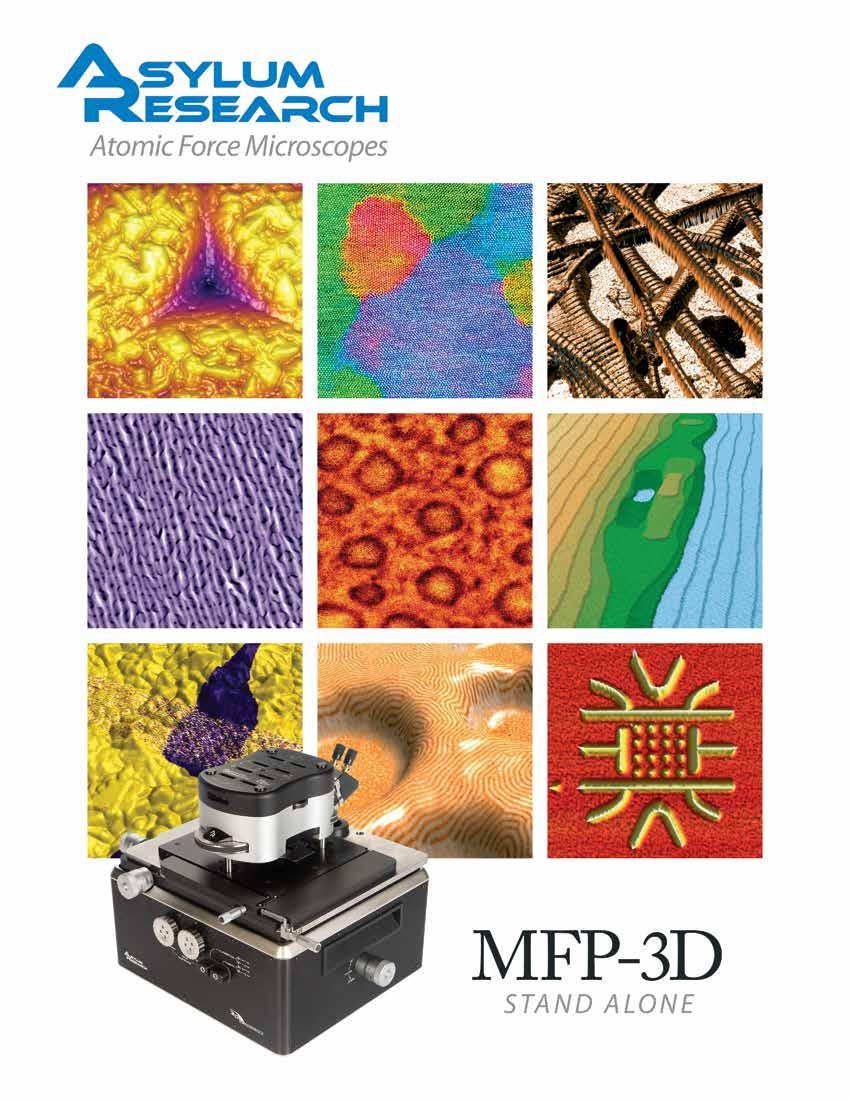
2 Head XY Scanner Base Technical Innovations TM Sensored, closed loop positioning for high resolution imaging, accuracy, and reproducibility. Pioneering all-digital controller for open software adaptability, power and flexibility. Built-in advanced features such as real-time 3D rendering, nanolithography/nanomanipulation, and Dual AC Mode for dual resonance and harmonic imaging. Designed for flexibility and expandability, with a wide range of available system, environmental and application options to enhance capabilities, including nanoindentation and Piezoresponse Force Microscopy (PFM). Please refer to the MFP-3D Options data sheet for details. Materials Science Devices Life Science Advanced Applications Aggregate of colloidosomes formed from the flash-curing of methacrylate emulsion droplets that are stabilized with 400nm PMMA latex spheres, 50μm scan. Iomega Zip 1GB drive write head. The MFM phase signal was overlaid on top of the topography, 20μm scan. Shewanella oneidensis strain MR-1 bacteria showing conductive bacterial nanowires, 5µm scan. Sample courtesy M. El-Naggar, USC and Y. Gorby, J. Craig Venter Institute. Nanoindentation on silicon, 1µm scan.

3 Designed by Scientists Who Understand the Demands of Your Research. Roger Proksch Jason Cleveland Co-founders Asylum Research was founded by scientists with the simple goal of creating the world s best research instrumentation for other scientists. We offer the most technically advanced Atomic Force Microscopes for applications such as materials science, life science, polymers, nanolithography, electrical/ magnetic measurements, and nanoindenting. Asylum Research sets the bar for AFM performance. Personalized, Exceptional Support Once you begin your research, our staff scientists are here to help you get the most out of your MFP-3D AFM. We extend this personalized support by being virtually in your lab with OnSight a remote support system that lets us view, diagnose and control your system over the Internet. Our easy, secure, web-based system enables shared screen, mouse and keyboard control of your AFM, making it ideal for training and troubleshooting. Asylum AFMs Have the Lowest Cost of Ownership A full one-year warranty is included with the MFP-3D-SA. Because of our robust, reliable systems, you can be sure that the cost of ownership will remain low even beyond the warranty period.

4 MFP-3D Head Low noise, eliminates interference Sensored optical lever with diffraction limited optics and a low coherence light source virtually eliminates interference artifacts. The NPS TM sensored Z axis provides precise measurements of the cantilever position for accurate force and topography measurements. Piezo Position Sensitive Detector Light Path Cantilever Z Flexure Stage Flexure Hinge Piezo Nanopositioning System (NPS) Sensor Optical Path L c =87nm pn To Cameras Cold Mirror MFP-3D XY Scanner Precision and accuracy unlike any tube scanner The MFP-3D uses a flexured scanner and patented NPS sensors which measure the exact position of each axis (X-Y). They correct for hysteresis and creep, providing flat scans and the ability to accurately zoom and offset with one mouse click. Recollimation Lens Sample Extension (nm) Mechanical Unfolding of Protein XY Flexure Hinge NPS Allows Precise Zooms NPS Sensor Piezo

5 To Cameras Bottom View Objective MFP-3D Base Three configurations for illuminating and viewing your sample Top view for opaque samples Bottom view for transparent samples Dual view for both viewing options Fiber Port for Köhler Illumination All-Digital Controller and Software Flexibility All-digital configuration allows virtually the entire system operation to be controlled through the MFP software interface (IGOR Pro) for easy addition of new microscope capabilities. What Kind of User Are You? New Experienced Power Built-in Features ModeMaster TM - A library of standard and user-defined operation modes such as AC, Contact, Phase, EFM, LFM, PFM, Force Mode, Nanolithography SmartStart TM - Auto configures any peripheral that interfaces with the controller for plug and play operation 25+ megapixel resolution MicroAngelo TM - Nanolithography and manipulation ARgyle TM - Real3D rendering both on and offline Channel Overlay Overlay data such as EFM or phase channel on topography IGOR Command and macro language at your disposal Edit and create your own automated MacroBuilder routines Software control of signal routing through crosspoint switch All-Digital ARC2 Controller 100% digital for low noise, fast operation, and flexibility Field Programmable Gate Array (FPGA) and Digital Signal Processor (DSP) Fast analog-to-digital/digital-to-analog conversions ARgyle Channel Overlay, Second Mode (Dual AC) Amplitude Image of ZnO, 1µm Scan.

6 Specifications Operating Modes Contact Mode: Imaging using feedback on deflection. Height, deflection, and lateral force signals available. AC and Dual AC : Q-controlled imaging using feedback on amplitude. Signals include height, amplitude/phase, I/Q, deflection; both air and fluid. Force Mode: Force curve acquisition in contact or AC mode. All signals available. Lateral Force: Frictional force imaging. MicroAngelo: Built-in nanolithography/ nanomanipulation. EFM, Surface Potential, Conductive AFM (CAFM) with ORCA (optional); Magnetic Force Microscopy (MFM), Variable Field MFM (optional); Piezoresponse Force Microscopy, Vector PFM, Switching Spectroscopy PFM (high voltage optional); Scanning Kelvin Probe Microscopy (SKPM); Nanoindentation (optional); Dual AC Resonance Tracking (DART); Thermal Analysis (optional) Data Acquisition Data size is limited only by the memory on the PC (i.e., 10 million point force curves and >5k x 5k point images are possible). It is possible to capture data at 5MHz for up to two million points continuously. Scan Axes X&Y: 90µm travel in closed loop. Closed loop position control with sensor noise <0.5nm average deviation (Adev) in a 0.1Hz-1kHz bandwidth (BW) and sensor nonlinearity <0.5% (max deviation/full travel) at full scan. Z: >15µm sensored travel. Sensor noise <0.25nm Adev in a 0.1Hz-1kHz BW and sensor non-linearity less than 0.05% (max deviation/full travel) at full scan. Z height: noise <0.06nm Adev, 0.1Hz-1kHz BW. Optical Lever Noise <0.02nm Adev in a 0.1Hz to 1kHz BW. Controller Electronics ADCs: One 16-bit input operating at 5MHz with seven gains and a 16-bit offset. Used primarily for cantilever deflection, but also user accessible; Five 16-bit inputs operating at 100kHz. Typically three are used for the reading of the X, Y, and Z sensors and two are available for user inputs. Frequency Synthesizer: Outputs from two Direct Digital Synthesizers (DDS) are summed and available on a 16-bit, 10MHz DAC. Frequency: DC to 2.0MHz in 2mHz increments. Amplitude: 0 to 20V(p-p) in 0.6mV increments. Amplitude, phase, and frequency of the oscillator can be controlled from software at 100kHz update rates. DACs: Six high resolution, ultra low-noise, fast 24- bit channels updated at 100kHz: two for XY scanning (14kHz bandwidth); one for Z feedback (117kHz bandwidth); and three general purpose (56kHz bandwidth). Digital Lock-ins: The 5MHz ADC is the input to two fully digital lock-ins that provide quadrature ouputs. Both R/ϑ (amplitude/phase) and I/Q (Rcosϑ/ Rsinϑ) are available in output bandwidths up to 9kHz. DSP: Floating point processor running at 80MHz. Digital Q-control: for cantilevers from 2kHz to 2MHz; typically enhances or suppresses Q by 5X. Computer-to-Controller Communication: Universal Serial Bus (USB). X, Y, & Z High Voltage Outputs: -10 to +150V. Computer: High-performance dual-monitor Windows computer (inquire for latest specifications and custom configurations). Light Source Superluminescent diode (SLD) is classified as Class 1M. Viewing with an optical instrument within a distance of 100mm may pose an eye hazard. Stage Micrometer driven stage for mechanical alignment of the cantilever tip and sample. MFP Head Standard Head: Flexure-mounted optical lever system with low-coherence SLD, liquid-compatible and AC-capable cantilever holder, dichroic mirror and window for optical access to cantilever, 80-pitch engage screws, and Invar shell. Extended Head (optional): 40µm Z scan range. Top View Head (optional): Adds 10x, 0.28 NA long-working distance objective with focus and beam steering adjustments, allows high resolution optical imaging of tip and sample. Narrowband Source (optional): Eliminates interference with sensitive optical experiments. High Bandwidth Photodiode (optional): Increases photodiode bandwidth for deflection and lateral signals to 7MHz. Base Models Stand Alone (SA): Three models are available. All feature bright field microscopy with Köhler illumination, adjustable aperture and field diaphragm, remote 150W light source coupled via fiber bundle, dual 1/4" CCD s with 720µm and 240µm fields of view; integrated scanning and interconnect board, and rigid low-vibration construction. Top View: Uses infinity-corrected Mitutoyo objective in Top View head for imaging of opaque samples at 3µm resolution. Bottom View: For transparent samples only. Default configuration is 10x/0.25 NA infinitycorrected objective. Others available upon request. Dual View: Combines features of Top and Bottom View, with switchable shutters. Allows for transmitted light in either direction. Sample Holders For samples up to 3.4"x1.5", including glass slides and coverslips. Specialized sample holders including flow-through and heating available (see Options Data Sheet). Software Open user interface based on IGOR Pro incorporates professional-quality analysis and graphing capabilities. AFM analysis includes section, histogram, roughness, particle analysis, and masking. Features include but not limited to: Nonlinear curve fitting to arbitrary user-defined functions. Extensive image analysis including 2D FFT s, wavelet transformations, convolutions, line profiles, particle analysis, edge detection (eight methods, including Sobel), and thresholding (five methods, including fuzzy entropy). Automatic spectral fitting and calibration of cantilever spring constants using thermal noise and Sader method. Easy generation of scientific publication quality graphs and page layouts. MFP-3D-SA is a Class 1M Laser Product ARgyle: OpenGL 3D rendering technology for advanced image display. Generate, display, and visualize 3D images in real-time while you scan as well as off-line processing. Overlay alternate channel data with primary to view feature correlation. Independent scaling of axes for true 1:1 aspect ratio. Mouse-driven rotating, panning, scaling, and specular lighting control of images. Export 3D images to clipboard, JPEG, TIFF, BMP, PNG, STL, VRML 2.0. Stereo anaglyph creation from 3D images. Vibration Isolation Vibration isolation is recommended for all systems. See Options Data Sheet. Additional Options A wide range of system, environmental, and application options are available to enhance the capabilities of the MFP-3D-SA. See MFP-3D Options Data Sheets for additional information Cover Images 1. Nanoindenting of indium tin oxide, 800nm scan. 2. Block copolymer self-organized into a close-packed lattice of spherical microdomains. Lattice orientation (color) overlaid on height data (light/dark) illustrates grain boundaries and defects, 16µm scan. Sample courtesy of M. Trawick, Univ. of Richmond. 3. Type I collagen imaged using Dual AC mode. Fundamental resonance phase data overlaid on AFM topography, 4µm scan. 4. Strain-induced corkscrew pattern on MBE grown AlGaAs, 12µm scan. Sample courtesy of T. Daniels-Race, LSU. 5. EFM photoinduced charging rate map generated by plotting the inverse exponential time constant for photoinduced charging at each point from the AFM image (not pictured). Dark rings indicate regions of slower charging. Image courtesy of D. Coffey and D. Ginger, Univ. of Washington. 6. Sapphire crystal following annealing at 1400 C leaving a clean surface with atomic steps (~3Å tall ) and occasional defects, 12µm scan. Image courtesy of S. MacLaren, UIUC. 7. Lead titanate film with PFM phase data overlaid on AFM topography, 5µm scan. Image courtesy of A. Gruverman and D. Wu, UNL. Sample courtesy H. Funakubo. 8. SEBS spuncoat onto a silicon wafer. Phase data overlaid on AFM topography, 2µm scan. Sample courtesy of R. Segalman and A. Hexemer, Kramer Group, UCSB. 9. Quantum dot structure created on a GaAs wafer using oxidation lithography, 2.5µm scan. Courtesy of D. Graf and R. Shleser, Ensslin Group, ETH Zurich. ARC2, ARgyle, Dual AC, MFP-3D, MicroAngelo, ModeMaster, MacroBuilder, NPS, ORCA, Real3D, and SmartStart are trademarks of Asylum Research. Other trademarks are those of their respective owners. Represented by: Hollister Avenue Santa Barbara, CA voice: fax: Toll free: sales@asylumresearch.com Specifications subject to change without notice Atomic Force Microscopes
INDIAN INSTITUTE OF TECHNOLOGY BOMBAY
 IIT Bombay requests quotations for a high frequency conducting-atomic Force Microscope (c-afm) instrument to be set up as a Central Facility for a wide range of experimental requirements. The instrument
Cutting-edge Atomic Force Microscopy techniques for large and multiple samples
 Cutting-edge Atomic Force Microscopy techniques for large and multiple samples Study of up to 200 mm samples using the widest set of AFM modes Industrial standards of automation A unique combination of
Asylum Research. MFP-3D Infinity. Endless Applications. Unlimited Potential. Performance / Versatility / Support
 MFP-3D Infinity AFM Asylum Research Endless Applications. Unlimited Potential. Performance / Versatility / Support MFP-3D Infinity AFM Asylum Research Endless applications. Unlimited potential. The Asylum
NanoFocus Inc. Next Generation Scanning Probe Technology. Tel : Fax:
 NanoFocus Inc. Next Generation Scanning Probe Technology www.nanofocus.kr Tel : 82-2-864-3955 Fax: 82-2-864-3956 Albatross SPM is Multi functional research grade system Flexure scanner and closed-loop
Nanosurf easyscan 2 FlexAFM
 Nanosurf easyscan 2 FlexAFM Your Versatile AFM System for Materials and Life Science www.nanosurf.com The new Nanosurf easyscan 2 FlexAFM scan head makes measurements in liquid as simple as measuring in
Park NX20 The leading nano metrology tool for failure analysis and large sample research.
 The Most Accurate Atomic Force Microscope Park NX20 The leading nano metrology tool for failure analysis and large sample research www.parkafm.com The Most Accurate Atomic Force Microscope Park NX20 The
Indian Institute of Technology Bombay
 Specifications for High Resolution Scanning Probe Microscope Item Essential measuring modes with complete hardware and software. All the modes should be demonstrated during installation & training Scanners
Measurement of Microscopic Three-dimensional Profiles with High Accuracy and Simple Operation
 238 Hitachi Review Vol. 65 (2016), No. 7 Featured Articles Measurement of Microscopic Three-dimensional Profiles with High Accuracy and Simple Operation AFM5500M Scanning Probe Microscope Satoshi Hasumura
10 Things to Consider when Acquiring a Nanopositioning System
 10 Things to Consider when Acquiring a Nanopositioning System There are many factors to consider when looking for nanopositioning piezo stages. This article will help explain some items that are important
Nanonics Systems are the Only SPMs that Allow for On-line Integration with Standard MicroRaman Geometries
 Nanonics Systems are the Only SPMs that Allow for On-line Integration with Standard MicroRaman Geometries 2002 Photonics Circle of Excellence Award PLC Ltd, England, a premier provider of Raman microspectral
Standard Operating Procedure of Atomic Force Microscope (Anasys afm+)
") Standard Operating Procedure of Atomic Force Microscope (Anasys afm+) The Anasys Instruments afm+ system incorporates an Atomic Force Microscope which can scan the sample in the contact mode and generate
Standard Operating Procedure of Atomic Force Microscope (Anasys afm+) The Anasys Instruments afm+ system incorporates an Atomic Force Microscope which can scan the sample in the contact mode and generate
SPM The Industry s Performance Leader High Resolution Closed-loop System Fast, Easy Tip & Sample Exchange Versatility and Value Powerful Research
 SPM The Industry s Performance Leader High Resolution Closed-loop System Fast, Easy Tip & Sample Exchange Versatility and Value Powerful Research Flexibility Atomic resolution STM image of highly-oriented
The NanomechPro Toolkit: Accurate Tools for Measuring Nanoscale Mechanical Properties for Diverse Materials
 NanomechPro Toolkit DATA SHEET 43 The NanomechPro Toolkit: Accurate Tools for Measuring Nanoscale Mechanical Properties for Diverse Materials Understanding nanoscale mechanical properties is of fundamental
The Most Accurate Atomic Force Microscope. Park NX20 The leading nano metrology tool for failure analysis and large sample research.
 The Most Accurate Atomic Force Microscope Park NX20 The leading nano metrology tool for failure analysis and large sample research www.parkafm.com Park Systems The Most Accurate Atomic Force Microscope
Optical Microscope. Active anti-vibration table. Mechanical Head. Computer and Software. Acoustic/Electrical Shield Enclosure
 Optical Microscope On-axis optical view with max. X magnification Motorized zoom and focus Max Field of view: mm x mm (depends on zoom) Resolution : um Working Distance : mm Magnification : max. X Zoom
MFP-3D-BIO. Asylum Research. The only full-capability AFM on an inverted optical microscope
 MFP-3D-BIO AFM Asylum Research The only full-capability AFM on an inverted optical microscope MFP-3D-BIO AFM Full-capability AFM integrated with optical microscopy The Asylum Research MFP-3D-BIO sets the
Electronic Characterization of Materials Using Conductive AFM
 Electronic Characterization of Materials Using Conductive AFM Amir Moshar Electrical Measurements SKPM EFM CAFM PFM SCM Non-Contact Electrical Techniques Scanning Kelvin Probe Microscopy Electric Force
Advanced Nanoscale Metrology with AFM
 Advanced Nanoscale Metrology with AFM Sang-il Park Corp. SPM: the Key to the Nano World Initiated by the invention of STM in 1982. By G. Binnig, H. Rohrer, Ch. Gerber at IBM Zürich. Expanded by the invention
University of MN, Minnesota Nano Center Standard Operating Procedure
 Equipment Name: Atomic Force Microscope Badger name: afm DI5000 PAN Revisionist Paul Kimani Model: Dimension 5000 Date: October 6, 2017 Location: Bay 1 PAN Revision: 1 A. Description i. Enhanced Motorized
attosnom I: Topography and Force Images NANOSCOPY APPLICATION NOTE M06 RELATED PRODUCTS G
 APPLICATION NOTE M06 attosnom I: Topography and Force Images Scanning near-field optical microscopy is the outstanding technique to simultaneously measure the topography and the optical contrast of a sample.
SENSOR+TEST Conference SENSOR 2009 Proceedings II
 B8.4 Optical 3D Measurement of Micro Structures Ettemeyer, Andreas; Marxer, Michael; Keferstein, Claus NTB Interstaatliche Hochschule für Technik Buchs Werdenbergstr. 4, 8471 Buchs, Switzerland Introduction
Atomic Force Microscopy (Bruker MultiMode Nanoscope IIIA)
") Atomic Force Microscopy (Bruker MultiMode Nanoscope IIIA) This operating procedure intends to provide guidance for general measurements with the AFM. For more advanced measurements or measurements with
Atomic Force Microscopy (Bruker MultiMode Nanoscope IIIA) This operating procedure intends to provide guidance for general measurements with the AFM. For more advanced measurements or measurements with
Outline: Introduction: What is SPM, history STM AFM Image treatment Advanced SPM techniques Applications in semiconductor research and industry
 1 Outline: Introduction: What is SPM, history STM AFM Image treatment Advanced SPM techniques Applications in semiconductor research and industry 2 Back to our solutions: The main problem: How to get nm
Lecture 20: Optical Tools for MEMS Imaging
 MECH 466 Microelectromechanical Systems University of Victoria Dept. of Mechanical Engineering Lecture 20: Optical Tools for MEMS Imaging 1 Overview Optical Microscopes Video Microscopes Scanning Electron
Nanoscale Material Characterization with Differential Interferometric Atomic Force Microscopy
 Nanoscale Material Characterization with Differential Interferometric Atomic Force Microscopy F. Sarioglu, M. Liu, K. Vijayraghavan, A. Gellineau, O. Solgaard E. L. Ginzton Laboratory University Tip-sample
UNIVERSITY OF WATERLOO Physics 360/460 Experiment #2 ATOMIC FORCE MICROSCOPY
 UNIVERSITY OF WATERLOO Physics 360/460 Experiment #2 ATOMIC FORCE MICROSCOPY References: http://virlab.virginia.edu/vl/home.htm (University of Virginia virtual lab. Click on the AFM link) An atomic force
LOW TEMPERATURE STM/AFM
 * CreaTec STM of Au(111) using a CO-terminated tip, 20mV bias, 0.6nA* LOW TEMPERATURE STM/AFM High end atomic imaging, spectroscopy and manipulation Designed and manufactured in Germany by CreaTec Fischer
R I T. Title: Wyko RST Plus. Semiconductor & Microsystems Fabrication Laboratory Revision: A Rev Date: 05/23/06 1 SCOPE 2 REFERENCE DOCUMENTS
 Approved by: Process Engineer / / / / Equipment Engineer 1 SCOPE The purpose of this document is to detail the use of the Wyko RST Plus. All users are expected to have read and understood this document.
Lateral Force: F L = k L * x
 Scanning Force Microscopy (SFM): Conventional SFM Application: Topography measurements Force: F N = k N * k N Ppring constant: Spring deflection: Pieo Scanner Interaction or force dampening field Contact
nanovea.com PROFILOMETERS 3D Non Contact Metrology
 PROFILOMETERS 3D Non Contact Metrology nanovea.com PROFILOMETER INTRO Nanovea 3D Non-Contact Profilometers are designed with leading edge optical pens using superior white light axial chromatism. Nano
Park XE7 The most affordable research grade AFM with flexible sample handling.
 Park XE7 The most affordable research grade AFM with flexible sample handling www.parkafm.com Park Systems The Most Accurate Atomic Force Microscope Park XE7 The economical choice for innovative research
- Near Field Scanning Optical Microscopy - Electrostatic Force Microscopy - Magnetic Force Microscopy
 - Near Field Scanning Optical Microscopy - Electrostatic Force Microscopy - Magnetic Force Microscopy Yongho Seo Near-field Photonics Group Leader Wonho Jhe Director School of Physics and Center for Near-field
Options and Accessories for Asylum Research MFP-3D AFMs
 ACCESSORIES Options and Accessories for Asylum Research MFP-3D AFMs Empower your research with powerful, innovative new capabilities Go beyond topography with advanced modes and environmental control Powerful
; A=4π(2m) 1/2 /h. exp (Fowler Nordheim Eq.) 2 const
 1/2 /h. exp (Fowler Nordheim Eq.) 2 const") Scanning Tunneling Microscopy (STM) Brief background: In 1981, G. Binnig, H. Rohrer, Ch. Gerber and J. Weibel observed vacuum tunneling of electrons between a sharp tip and a platinum surface. The tunnel
Scanning Tunneling Microscopy (STM) Brief background: In 1981, G. Binnig, H. Rohrer, Ch. Gerber and J. Weibel observed vacuum tunneling of electrons between a sharp tip and a platinum surface. The tunnel
Coherent Laser Measurement and Control Beam Diagnostics
 Coherent Laser Measurement and Control M 2 Propagation Analyzer Measurement and display of CW laser divergence, M 2 (or k) and astigmatism sizes 0.2 mm to 25 mm Wavelengths from 220 nm to 15 µm Determination
PICO MASTER 200. UV direct laser writer for maskless lithography
 PICO MASTER 200 UV direct laser writer for maskless lithography 4PICO B.V. Jan Tinbergenstraat 4b 5491 DC Sint-Oedenrode The Netherlands Tel: +31 413 490708 WWW.4PICO.NL 1. Introduction The PicoMaster
Park NX10. The most accurate and easiest to use Atomic Force Microscope.
 The most accurate and easiest to use Atomic Force Microscope www.parkafm.com Park Systems Enabling Nanoscale Advances The premiere choice for nanotechnology research Better data Park NX10 produces data
taccor Optional features Overview Turn-key GHz femtosecond laser
 taccor Turn-key GHz femtosecond laser Self-locking and maintaining Stable and robust True hands off turn-key system Wavelength tunable Integrated pump laser Overview The taccor is a unique turn-key femtosecond
OPTICS IN MOTION. Introduction: Competing Technologies: 1 of 6 3/18/2012 6:27 PM.
 1 of 6 3/18/2012 6:27 PM OPTICS IN MOTION STANDARD AND CUSTOM FAST STEERING MIRRORS Home Products Contact Tutorial Navigate Our Site 1) Laser Beam Stabilization to design and build a custom 3.5 x 5 inch,
Supplementary Figure 1
 Supplementary Figure 1 Technical overview drawing of the Roadrunner goniometer. The goniometer consists of three main components: an inline sample-viewing microscope, a high-precision scanning unit for
Manufacturing Metrology Team
 The Team has a range of state-of-the-art equipment for the measurement of surface texture and form. We are happy to discuss potential measurement issues and collaborative research Manufacturing Metrology
Synergy ESPM 3-D Environmental Scanning Probe Microscope Operation Manual
 Synergy ESPM 3-D Environmental Scanning Probe Microscope Operation Manual Manufactured in the USA Rev. 01/2005 1. Introduction What Is Atomic Force Microscopy? 3 2. Getting Started Introduction 4 What
Microscopic Structures
 Microscopic Structures Image Analysis Metal, 3D Image (Red-Green) The microscopic methods range from dark field / bright field microscopy through polarisation- and inverse microscopy to techniques like
Difrotec Product & Services. Ultra high accuracy interferometry & custom optical solutions
 Difrotec Product & Services Ultra high accuracy interferometry & custom optical solutions Content 1. Overview 2. Interferometer D7 3. Benefits 4. Measurements 5. Specifications 6. Applications 7. Cases
Investigate in magnetic micro and nano structures by Magnetic Force Microscopy (MFM)
") Investigate in magnetic micro and nano 5.3.85- Related Topics Magnetic Forces, Magnetic Force Microscopy (MFM), phase contrast imaging, vibration amplitude, resonance shift, force Principle Caution! -
Investigate in magnetic micro and nano 5.3.85- Related Topics Magnetic Forces, Magnetic Force Microscopy (MFM), phase contrast imaging, vibration amplitude, resonance shift, force Principle Caution! -
NOVA S12. Compact and versatile high performance camera system. 1-Megapixel CMOS Image Sensor: 1024 x 1024 pixels at 12,800fps
 NOVA S12 1-Megapixel CMOS Image Sensor: 1024 x 1024 pixels at 12,800fps Maximum Frame Rate: 1,000,000fps Class Leading Light Sensitivity: ISO 12232 Ssat Standard ISO 64,000 monochrome ISO 16,000 color
Imaging Carbon Nanotubes Magdalena Preciado López, David Zahora, Monica Plisch
 Imaging Carbon Nanotubes Magdalena Preciado López, David Zahora, Monica Plisch I. Introduction In this lab you will image your carbon nanotube sample from last week with an atomic force microscope. You
The Most Accurate Atomic Force Microscope. Park XE15 Power and versatility, brilliantly combined.
 The Most Accurate Atomic Force Microscope Park XE15 Power and versatility, brilliantly combined. www.parkafm.com Park XE15 Increase your productivity with our powerfully versatile atomic force microscope
Nanosurf Nanite. Automated AFM for Industry & Research.
 Nanosurf Nanite Automated AFM for Industry & Research www.nanosurf.com Multiple Measurements Automated Got work? Nanosurf has the solution! The Swiss-based innovator and manufacturer of the most compact
AFM of High-Profile Surfaces
 AFM of High-Profile Surfaces Fig. 1. AFM topograpgy image of black Si made using SCD probe tip. Scan size 4. Profile height is more than 8. See details and other application examples below. High Aspect
Introduction of New Products
 Field Emission Electron Microscope JEM-3100F For evaluation of materials in the fields of nanoscience and nanomaterials science, TEM is required to provide resolution and analytical capabilities that can
Park NX-Hivac The world s most accurate and easy to use high vacuum AFM for failure analysis.
 Park NX-Hivac The world s most accurate and easy to use high vacuum AFM for failure analysis www.parkafm.com Park NX-Hivac High vacuum scanning for failure analysis applications 4 x 07 / Cm3 Current (µa)
Figure for the aim4np Report
 Figure for the aim4np Report This file contains the figures to which reference is made in the text submitted to SESAM. There is one page per figure. At the beginning of the document, there is the front-page
7 CHAPTER 7: REFRACTIVE INDEX MEASUREMENTS WITH COMMON PATH PHASE SENSITIVE FDOCT SETUP
 7 CHAPTER 7: REFRACTIVE INDEX MEASUREMENTS WITH COMMON PATH PHASE SENSITIVE FDOCT SETUP Abstract: In this chapter we describe the use of a common path phase sensitive FDOCT set up. The phase measurements
Atomic Force Microscopes
 Nanoscale Surface Characterization tomic Force Microscopes www.witec.de WITec tomic Force Microscopes Nanoscale Surface Characterization The WITec tomic Force Microscope (FM) module integrated with a research-grade
ATOMIC FORCE MICROSCOPY
 B47 Physikalisches Praktikum für Fortgeschrittene Supervision: Prof. Dr. Sabine Maier sabine.maier@physik.uni-erlangen.de ATOMIC FORCE MICROSCOPY Version: E1.4 first edit: 15/09/2015 last edit: 05/10/2018
Keysight 9500 AFM. Data Sheet
 Keysight 9500 AFM Data Sheet System Overview The Keysight Technologies, Inc. 9500 AFM seamlessly integrates revolutionary new software, a new high-bandwidth digital controller, and a state-of-the-art mechanical
1.6 Beam Wander vs. Image Jitter
 8 Chapter 1 1.6 Beam Wander vs. Image Jitter It is common at this point to look at beam wander and image jitter and ask what differentiates them. Consider a cooperative optical communication system that
Advanced 3D Optical Profiler using Grasshopper3 USB3 Vision camera
 Advanced 3D Optical Profiler using Grasshopper3 USB3 Vision camera Figure 1. The Zeta-20 uses the Grasshopper3 and produces true color 3D optical images with multi mode optics technology 3D optical profiling
Large Signal Displacement Measurement with an Asylum SA Atomic Force Microscope Rev B
 Radiant Technologies, Inc. 2835D Pan American Freeway NE Albuquerque, NM 87107 Tel: 505-842-8007 Fax: 505-842-0366 e-mail: radiant@ferrodevices.com www.ferrodevices.com Large Signal Displacement Measurement
Standard Operating Procedure
 Standard Operating Procedure Nanosurf Atomic Force Microscopy Operation Facility NCCRD Nanotechnology Center for Collaborative Research and Development Department of Chemistry and Engineering Physics The
ASM Webinar Digital Microscopy for Materials Science
 Digital Microscopy Defined The term Digital Microscopy applies to any optical platform that integrates a digital camera and software to acquire images; macroscopes, stereomicroscopes, compound microscopes
Rebirth of Force Spectroscopy: Advanced Nanomechanical, Electrical, Optical, Thermal and Piezoresponse Studies
 HybriD Mode Rebirth of Force Spectroscopy: Advanced Nanomechanical, Electrical, Optical, Thermal and Piezoresponse Studies Fast Quantitative Nanomechanical Measurements and Force Volume Simultaneous Electrostatic
Ionscope SICM. About Ionscope. Scanning Ion Conductance Microscopy. Ionscope A brand of Openiolabs Limited
 SICM About is a brand of openiolabs Ltd, headquartered in Cambridge UK, is the world-leader in (SICM), a rapidly emerging Scanning Probe Microscopy (SPM) technique which allows nanoscale topographical
Camera Overview. Digital Microscope Cameras for Material Science: Clear Images, Precise Analysis. Digital Cameras for Microscopy
 Digital Cameras for Microscopy Camera Overview For Materials Science Microscopes Digital Microscope Cameras for Material Science: Clear Images, Precise Analysis Passionate about Imaging: Olympus Digital
Information & Instructions
 KEY FEATURES 1. USB 3.0 For the Fastest Transfer Rates Up to 10X faster than regular USB 2.0 connections (also USB 2.0 compatible) 2. High Resolution 4.2 MegaPixels resolution gives accurate profile measurements
Instructions for easyscan Atomic Force Microscope
 UVA's Hands-on Introduction to Nanoscience Instructions for easyscan Atomic Force Microscope (revision 8 November 2012) NOTE: Instructions assume software is pre-configured per "UVA Instructor Guide for
Fully depleted, thick, monolithic CMOS pixels with high quantum efficiency
 Fully depleted, thick, monolithic CMOS pixels with high quantum efficiency Andrew Clarke a*, Konstantin Stefanov a, Nicholas Johnston a and Andrew Holland a a Centre for Electronic Imaging, The Open University,
PicoMaster 100. Unprecedented finesse in creating 3D micro structures. UV direct laser writer for maskless lithography
 UV direct laser writer for maskless lithography Unprecedented finesse in creating 3D micro structures Highest resolution in the market utilizing a 405 nm diode laser Structures as small as 300 nm 375 nm
Constant Frequency / Lock-In (AM-AFM) Constant Excitation (FM-AFM) Constant Amplitude (FM-AFM)
 Constant Excitation (FM-AFM) Constant Amplitude (FM-AFM)") HF2PLL Phase-locked Loop Connecting an HF2PLL to a Bruker Icon AFM / Nanoscope V Controller Zurich Instruments Technical Note Keywords: AM-AFM, FM-AFM, AFM control Release date: February 2012 Introduction
HF2PLL Phase-locked Loop Connecting an HF2PLL to a Bruker Icon AFM / Nanoscope V Controller Zurich Instruments Technical Note Keywords: AM-AFM, FM-AFM, AFM control Release date: February 2012 Introduction
Atomic Scale Patterning Made Easy
 ZyVector STM Control System for Atomically Precise Lithography Making Atomic Resolution Lithography a reality Distributed by Distortion-Free Imaging Automatic Lattice Alignment Digital Vector Lithography
Dual-channel Lock-in Amplifier Module
 Dual-channel Lock-in Amplifier Module Introduction Phase-locked amplification and demodulation techniques of weak signals have a wide range of applications in Turnable Diode Laser Absorption Spectrum (TDLAS)
Technical Explanation for Displacement Sensors and Measurement Sensors
 Technical Explanation for Sensors and Measurement Sensors CSM_e_LineWidth_TG_E_2_1 Introduction What Is a Sensor? A Sensor is a device that measures the distance between the sensor and an object by detecting
Radial Polarization Converter With LC Driver USER MANUAL
 ARCoptix Radial Polarization Converter With LC Driver USER MANUAL Arcoptix S.A Ch. Trois-portes 18 2000 Neuchâtel Switzerland Mail: info@arcoptix.com Tel: ++41 32 731 04 66 Principle of the radial polarization
Basic methods in imaging of micro and nano structures with atomic force microscopy (AFM)
") Basic methods in imaging of micro and nano P2538000 AFM Theory The basic principle of AFM is very simple. The AFM detects the force interaction between a sample and a very tiny tip (
Basic methods in imaging of micro and nano P2538000 AFM Theory The basic principle of AFM is very simple. The AFM detects the force interaction between a sample and a very tiny tip (
Zeta-300 3D OPTICAL PROFILER
 Zeta-300 3D OPTICAL PROFILER Technology Toolkit Developed in 2007, the revolutionary Confocal Grid Structured Illumination (CGSI) is the powerful technology in all Zeta Optical Profilers but in a Zeta,
Suivie de résonance: méthodes à fréquences multiples. Romain Stomp Application Scientist, Zurich Instruments AG. ZI Applications
 Suivie de résonance: méthodes à fréquences multiples Romain Stomp Application Scientist, Zurich Instruments AG Slide 1 Sommaire 1. Un peu de traitement du signal pour le SPM Détection synchrone pour le
Microscopy. The dichroic mirror is an important component of the fluorescent scope: it reflects blue light while transmitting green light.
 Microscopy I. Before coming to lab Read this handout and the background. II. Learning Objectives In this lab, you'll investigate the physics of microscopes. The main idea is to understand the limitations
Imaging and Spectroscopy Applications Guide
 SPM Applications Guide USER GUIDE 3 Imaging and Spectroscopy Applications Guide User Guide including beta (complete, reviewed) chapters, including draft (nearly complete, not reviewed) chapters, Versionα,
Cavity QED with quantum dots in semiconductor microcavities
 Cavity QED with quantum dots in semiconductor microcavities M. T. Rakher*, S. Strauf, Y. Choi, N.G. Stolz, K.J. Hennessey, H. Kim, A. Badolato, L.A. Coldren, E.L. Hu, P.M. Petroff, D. Bouwmeester University
Frequency Response Analyzers for Stability Analysis and Power Electronics Performance Testing
 Frequency Response Analyzers for Stability Analysis and Power Electronics Performance Testing Product Features Since 1979, Venable Instruments has been focused on one goal: bringing the most versatile,
Camera Overview. Digital Microscope Cameras for Material Science: Clear Images, Precise Analysis. Digital Cameras for Microscopy
 Digital Cameras for Microscopy Camera Overview For Materials Science Microscopes Digital Microscope Cameras for Material Science: Clear Images, Precise Analysis Passionate about Imaging: Olympus Digital
attocube systems Probe Stations for Extreme Environments CRYOGENIC PROBE STATION fundamentals principles of cryogenic probe stations
 PAGE 88 & 2008 2007 PRODUCT CATALOG CRYOGENIC PROBE STATION fundamentals...................... 90 principles of cryogenic probe stations attocps I.......................... 92 ultra stable cryogenic probe
Things to check before start-up.
 Byeong Cha Page 1 11/24/2009 Manual for Leica SP2 Confocal Microscope Enter you name, the date, the time, and the account number in the user log book. Things to check before start-up. Make sure that your
Supporting Information 1. Experimental
 Supporting Information 1. Experimental The position markers were fabricated by electron-beam lithography. To improve the nanoparticle distribution when depositing aqueous Ag nanoparticles onto the window,
ArbStudio Arbitrary Waveform Generators. Powerful, Versatile Waveform Creation
 ArbStudio Arbitrary Waveform Generators Powerful, Versatile Waveform Creation UNMATCHED WAVEFORM UNMATCHED WAVEFORM GENERATION GENERATION Key Features 125 MHz bandwidth 1 GS/s maximum sample rate Long
Micro-manipulated Cryogenic & Vacuum Probe Systems
 Janis micro-manipulated probe stations are designed for non-destructive electrical testing using DC, RF, and fiber-optic probes. They are useful in a variety of fields including semiconductors, MEMS, superconductivity,
ScanArray Overview. Principle of Operation. Instrument Components
 ScanArray Overview The GSI Lumonics ScanArrayÒ Microarray Analysis System is a scanning laser confocal fluorescence microscope that is used to determine the fluorescence intensity of a two-dimensional
SIGNAL RECOVERY. Model 7265 DSP Lock-in Amplifier
 Model 7265 DSP Lock-in Amplifier FEATURES 0.001 Hz to 250 khz operation Voltage and current mode inputs Direct digital demodulation without down-conversion 10 µs to 100 ks output time constants Quartz
Study of shear force as a distance regulation mechanism for scanning near-field optical microscopy
 Study of shear force as a distance regulation mechanism for scanning near-field optical microscopy C. Durkan a) and I. V. Shvets Department of Physics, Trinity College Dublin, Ireland Received 31 May 1995;
Akiyama-Probe (A-Probe) guide
 guide") Akiyama-Probe (A-Probe) guide This guide presents: what is Akiyama-Probe, how it works, and what you can do Dynamic mode AFM Version: 2.0 Introduction NANOSENSORS Akiyama-Probe (A-Probe) is a self-sensing
Akiyama-Probe (A-Probe) guide This guide presents: what is Akiyama-Probe, how it works, and what you can do Dynamic mode AFM Version: 2.0 Introduction NANOSENSORS Akiyama-Probe (A-Probe) is a self-sensing
Figure 4.1 Vector representation of magnetic field.
 Chapter 4 Design of Vector Magnetic Field Sensor System 4.1 3-Dimensional Vector Field Representation The vector magnetic field is represented as a combination of three components along the Cartesian coordinate
MS260i 1/4 M IMAGING SPECTROGRAPHS
 MS260i 1/4 M IMAGING SPECTROGRAPHS ENTRANCE EXIT MS260i Spectrograph with 3 Track Fiber on input and InstaSpec IV CCD on output. Fig. 1 OPTICAL CONFIGURATION High resolution Up to three gratings, with
Electro-optic Spectral Decoding Measurements at FLASH
 Electro-optic Spectral Decoding Measurements at FLASH, FLA Florian Loehl, Sebastian Schulz, Laurens Wißmann Motivation Development of a robust online bunch length monitor for FLASH and XFEL Transition
Large Signal Displacement Measurement with an MTI Photonic Sensor Rev B
 Radiant Technologies, Inc. 2835D Pan American Freeway NE Albuquerque, NM 8717 Tel: 55-842-87 Fax: 55-842-366 e-mail: radiant@ferrodevices.com www.ferrodevices.com Large Signal Displacement Measurement
FlexDDS-NG DUAL. Dual-Channel 400 MHz Agile Waveform Generator
 FlexDDS-NG DUAL Dual-Channel 400 MHz Agile Waveform Generator Excellent signal quality Rapid parameter changes Phase-continuous sweeps High speed analog modulation Wieserlabs UG www.wieserlabs.com FlexDDS-NG
Comparison of resolution specifications for micro- and nanometer measurement techniques
 P4.5 Comparison of resolution specifications for micro- and nanometer measurement techniques Weckenmann/Albert, Tan/Özgür, Shaw/Laura, Zschiegner/Nils Chair Quality Management and Manufacturing Metrology
Akiyama-Probe (A-Probe) guide
 guide") Akiyama-Probe (A-Probe) guide This guide presents: what is Akiyama-Probe, how it works, and its performance. Akiyama-Probe is a patented technology. Version: 2009-03-23 Introduction NANOSENSORS Akiyama-Probe
Akiyama-Probe (A-Probe) guide This guide presents: what is Akiyama-Probe, how it works, and its performance. Akiyama-Probe is a patented technology. Version: 2009-03-23 Introduction NANOSENSORS Akiyama-Probe
Nanosurf easyscan 2 Your Modular Scanning Probe Microscopy System
 Nanosurf Your Modular Scanning Probe Microscopy System www.nanosurf.com Perfect Modularity Nanosurf s easyscan series has gained worldwide popularity through its affordability, portability, and ease of
Angular Drift of CrystalTech (1064nm, 80MHz) AOMs due to Thermal Transients. Alex Piggott
 AOMs due to Thermal Transients. Alex Piggott") Angular Drift of CrystalTech 38 197 (164nm, 8MHz) AOMs due to Thermal Transients Alex Piggott July 5, 21 1 .1 General Overview of Findings The AOM was found to exhibit significant thermal drift effects,
Angular Drift of CrystalTech 38 197 (164nm, 8MHz) AOMs due to Thermal Transients Alex Piggott July 5, 21 1 .1 General Overview of Findings The AOM was found to exhibit significant thermal drift effects,