Planar micro-optic solar concentration. Jason H. Karp
|
|
|
- Britney Bradley
- 6 years ago
- Views:
Transcription


1 Planar micro-optic solar concentration Jason H. Karp Eric J. Tremblay, Katherine A. Baker and Joseph E. Ford Photonics Systems Integration Lab University of California San Diego Jacobs School of Engineering November 10, 2009 PHOTONIC SYSTEMS INTEGRATION LABORATORY UCSD JACOBS SCHOOL OF ENGINEERING Photo: Kevin Walsh, OLR
 Dr. Joseph E.")

 8-fold")


 Group")

2 Photonic Systems Integration Lab (PSI) Dr. Joseph E. Ford Principle Investigator Photonic Systems Integration Lab Concentric Multi-reflection Lenses (aka Origami Optics) 8-fold telephoto lens, 40mm focal length, 5mm thick 5.7 full angle field of view E. Tremblay, R. Stack, R. Morrison, J. Karp, and J. Ford, "Ultrathin four-reflection imager," Appl. Opt. 48, (2009) Group Members: Stephen Olivas Eric Tremblay Brett Nadler Jason Karp Justin Hallas Kate Baker Pavel Shekhtmeyster
 Silicon Solar Cells")


3 Concentrator Photovoltaics (CPV) Silicon Solar Cells Single material bandgap 12-18% efficiency Multijunction Solar Cells 2 or more material bandgaps >40% efficiency GaInP GaInAs Solar Concentration 100x 500x increase in flux Ge Goal: Design and fabricate a highflux concentrator compatible with inexpensive manufacturing


4 Concentrator Components Solar Systems 1. Primary Focusing Optic Performs light concentration Large collecting lens or mirror Trend towards multiple apertures Energy Innovations SolFocus 2. Secondary Homogenization Optic Mounted between primary and PV cell Uniform illumination for high efficiency Non-imaging optical design Light Prescriptions Innovators Xiaohui Ning, Appl. Opt. 26, Mechanical Tracking Alignment for direct insolation Angular acceptance defines tracking accuracy Wind loading and environmental stability Flatcon System Tracking Concentrix Solar

 Focused Sunlight Decoupling Loss")


5 Optical design & modeling Multiple apertures couple to single output Homogeneous output intensity Uniform thickness (roll-to-roll fabrication) Focused Sunlight Decoupling Loss Slab waveguide symmetric prism coupling J. H. Karp, E. J. Tremblay and J. E. Ford, Planar micro-optic solar concentrator, Optics Express, Submitted for publication, October 12, Reflective prisms tilt light to TIR Couplers occupy <0.1% of waveguide surface Subsequent interaction decouples as loss


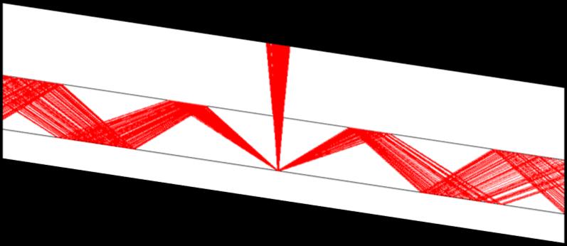


6 System Layout Lens Array Cladding Layer Slab Waveguide Slab Thickness Geometric Concentration Ratio Slab Length Cgeo 2x Slab Thickness

 rotational alignment UV Exposure Solution: Self-alignment")


7 Fabrication process: Self-alignment Critical Alignment Tolerance Lens focus must overlap with each coupling location <50μm lateral alignment tolerance <0.01 (0.2mrad) rotational alignment UV Exposure Solution: Self-alignment Mold prism structure in UV-curable photopolymer Expose through lens array to define coupling regions Cured regions remain part of the final device Coupling features made by exposure through lenses Low-cost manufacturing process Continuous roll processing (same used for holographic packaging) on flexible or rigid substrates


8 Design Tradeoffs Field Displacement: Sun subtends ±0.25 θ θ d f tanθ d f tanθ f f Short focal length small coupling area Long focal length easier TIR condition Waveguide Thickness: C flux = Slab Length Slab Thickness x Efficiency Length Slab Thickness Length Slab Thickness Thin waveguide high concentration Thick waveguide increased efficiency


9 Zemax Raytracing Model Zemax Non-Sequential Model Lens aberrations Polychromatic illumination Material dispersion Coatings and surface reflections Air Cladding Design 100μm air spacing Supports steep ray angles All glass construction 1mm thick waveguide F/2.45 lenses Fluoropolymer Cladding Low index cladding (n=1.33) Solid profile Polymer lens, glass waveguide 1mm thick waveguide F/4.11 lenses J. H. Karp, E. J. Tremblay and J. E. Ford, Planar micro-optic solar concentrator, Optics Express, Submitted for publication, October 12, 2009.
10 Broad Spectrum Performance Optimized for nm sunlight Accurate range of material models Minimum bandwidth for multi-junction PV cells

11 Fabrication Process 1. Spin SU-8 and Softbake 5. UV Exposure UV Exposure Source 2. Apply Mold and Pull Vacuum Hg arc aspheric collector collimating mirror beam expansion and iris T T 3. Bake Under Weight 6. Deposit Reflective Coating 6 diameter beam 1kg 4. Separate Mold and Invert 7. Heat Above T g and Develop Uniform, collimated UV illumination Hg arc lamp Waveguide Un-crosslinked SU-8 Prism Mold Crosslinked SU-8 Lens Array PHOTONIC SYSTEMS INTEGRATION LABORATORY UCSD JACOBS SCHOOL OF ENGINEERING Adjust beam divergence using the iris
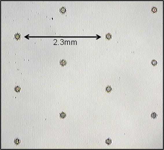
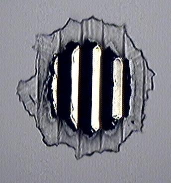
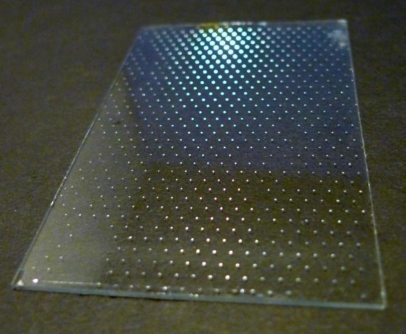
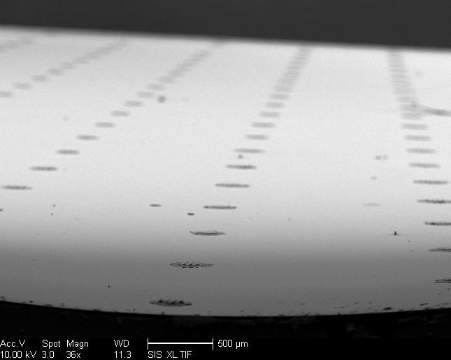
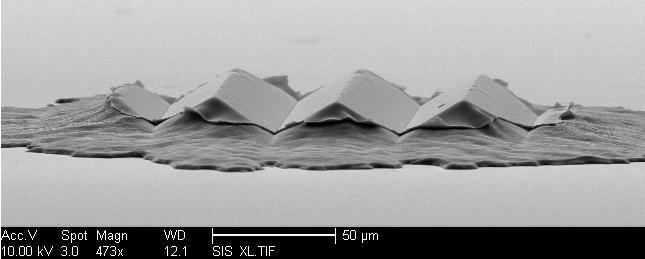
12 Fabricated Couplers Al-coated prism facet 75mm Transparent glass slab 50μm 50mm 200μm 20µm Depth


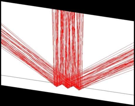
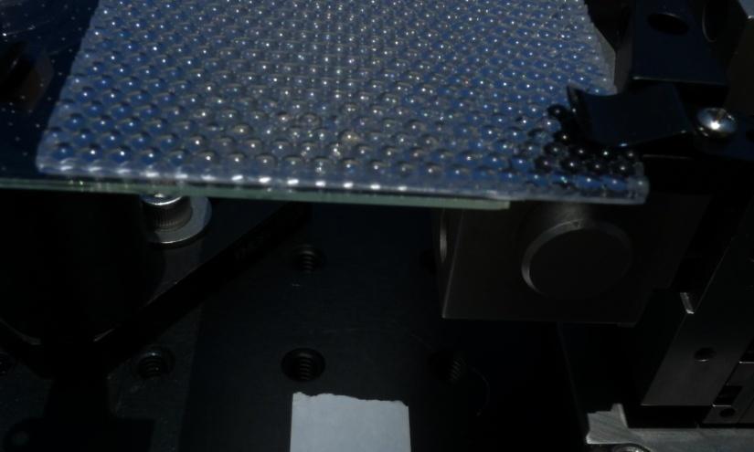
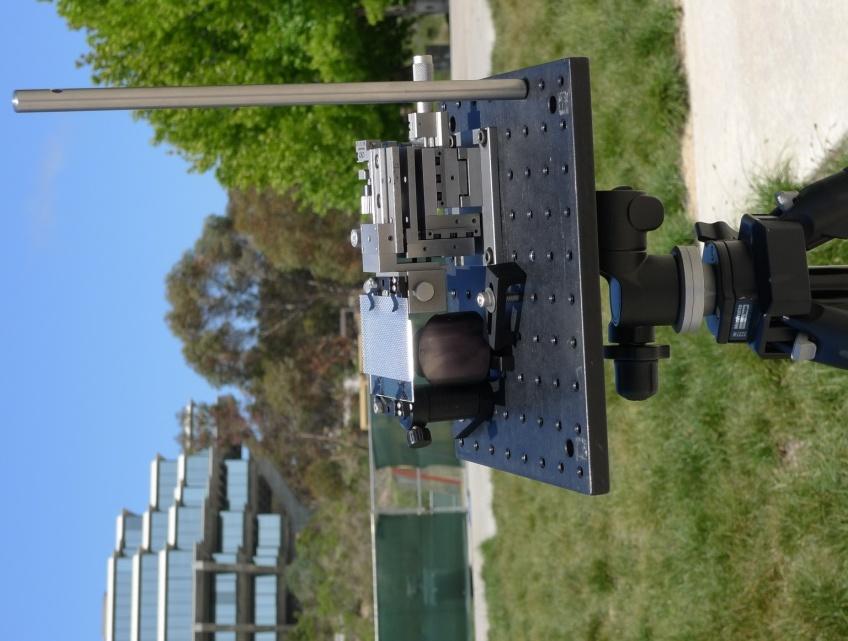
13 Prototype Testing Alignment stage Calibrated detector Illuminated prototype Lens Array ±0.25 Illumination Waveguide 44.8% simulated efficiency 32.4% measured efficiency ±1.0 angular acceptance Non-ideal lens array Very short focal length Aberrations Large spots Low fill-factor (72.5%) 27.5% loss 72.5% fill

14 Solar Illumination Testing Aligned Misaligned


15 Future Directions 2 nd Prototype concentrator Replace existing lens array >65% predicted efficiency Integrate with PV cell Orthogonal focusing Additional concentration Secondary extraction Orthogonal focusing Spectral band splitting Dichroic output edges Tilt/roll tracking platform PV Cell Tracking System Design

")
, Energy")

16 This research is supported by: National Science Foundation (NSF), Small Grants for Exploratory Research (SGER) program California Energy Commission (CEC), Energy Innovations Small Grant (EISG) program Thank You Website:
Micro-Optic Solar Concentration and Next-Generation Prototypes
 Micro-Optic Solar Concentration and Next-Generation Prototypes Jason H. Karp, Eric J. Tremblay and Joseph E. Ford Photonics Systems Integration Lab University of California San Diego Jacobs School of Engineering
Radial Coupling Method for Orthogonal Concentration within Planar Micro-Optic Solar Collectors
 Radial Coupling Method for Orthogonal Concentration within Planar Micro-Optic Solar Collectors Jason H. Karp, Eric J. Tremblay and Joseph E. Ford Photonics Systems Integration Lab University of California
Multiband Solar Concentrator using Transmissive Dichroic Beamsplitting
 Multiband Solar Concentrator using Transmissive Dichroic Beamsplitting Jason H. Karp and Joseph E. Ford Photonics Systems Integration Lab University of California, San Diego Jacobs School of Engineering
Solar Optical Design. It s an imaging problem. Mike Sullivan November 2008
 Solar Optical Design It s an imaging problem Mike Sullivan November 2008 2 www.kiarabio.com 3 Outline Design Problem Solar Spectrum and Detectors Concentration Defined Direct Imaging Pupil imaging Concentrator
 Efficiency of an Ideal Solar Cell (Henry, C. H. J. Appl. Phys. 51, 4494) No absorption radiative recombination loss Thermalization loss Efficiencies of multi-band-gap Solar Cell (Henry, C. H. J. Appl.
Fast, Two-Dimensional Optical Beamscanning by Wavelength Switching T. K. Chan, E. Myslivets, J. E. Ford
 Photonics Systems Integration Lab University of California San Diego Jacobs School of Engineering Fast, Two-Dimensional Optical Beamscanning by Wavelength Switching T. K. Chan, E. Myslivets, J. E. Ford
Deformable MEMS Micromirror Array for Wavelength and Angle Insensitive Retro-Reflecting Modulators Trevor K. Chan & Joseph E. Ford
 Photonics Systems Integration Lab UCSD Jacobs School of Engineering Deformable MEMS Micromirror Array for Wavelength and Angle Insensitive Retro-Reflecting Modulators Trevor K. Chan & Joseph E. Ford PHOTONIC
EUV Plasma Source with IR Power Recycling
 1 EUV Plasma Source with IR Power Recycling Kenneth C. Johnson kjinnovation@earthlink.net 1/6/2016 (first revision) Abstract Laser power requirements for an EUV laser-produced plasma source can be reduced
Figure 7 Dynamic range expansion of Shack- Hartmann sensor using a spatial-light modulator
 Figure 4 Advantage of having smaller focal spot on CCD with super-fine pixels: Larger focal point compromises the sensitivity, spatial resolution, and accuracy. Figure 1 Typical microlens array for Shack-Hartmann
OPTIMIZING CPV SYSTEMS FOR THERMAL AND SPECTRAL TOLERANCE
 OPTIMIZING CPV SYSTEMS FOR THERMAL AND SPECTRAL TOLERANCE S. Askins* 1, M. Victoria Pérez 1, R. Herrero 1, C. Domínguez 1, I. Anton 1, G. Sala 1, A. Coutinho 2, J.C. Amador 2 1 Instituto de Energía Solar
A novel tunable diode laser using volume holographic gratings
 A novel tunable diode laser using volume holographic gratings Christophe Moser *, Lawrence Ho and Frank Havermeyer Ondax, Inc. 85 E. Duarte Road, Monrovia, CA 9116, USA ABSTRACT We have developed a self-aligned
Wavelength Stabilization of HPDL Array Fast-Axis Collimation Optic with integrated VHG
 Wavelength Stabilization of HPDL Array Fast-Axis Collimation Optic with integrated VHG C. Schnitzler a, S. Hambuecker a, O. Ruebenach a, V. Sinhoff a, G. Steckman b, L. West b, C. Wessling c, D. Hoffmann
Design Description Document
 UNIVERSITY OF ROCHESTER Design Description Document Flat Output Backlit Strobe Dare Bodington, Changchen Chen, Nick Cirucci Customer: Engineers: Advisor committee: Sydor Instruments Dare Bodington, Changchen
Optical Bus for Intra and Inter-chip Optical Interconnects
 Optical Bus for Intra and Inter-chip Optical Interconnects Xiaolong Wang Omega Optics Inc., Austin, TX Ray T. Chen University of Texas at Austin, Austin, TX Outline Perspective of Optical Backplane Bus
Understanding Optical Specifications
 Understanding Optical Specifications Optics can be found virtually everywhere, from fiber optic couplings to machine vision imaging devices to cutting-edge biometric iris identification systems. Despite
Micro- and Nano-Technology... for Optics
 Micro- and Nano-Technology...... for Optics 3.2 Lithography U.D. Zeitner Fraunhofer Institut für Angewandte Optik und Feinmechanik Jena Printing on Stones Map of Munich Stone Print Contact Printing light
Use of Computer Generated Holograms for Testing Aspheric Optics
 Use of Computer Generated Holograms for Testing Aspheric Optics James H. Burge and James C. Wyant Optical Sciences Center, University of Arizona, Tucson, AZ 85721 http://www.optics.arizona.edu/jcwyant,
Assembly and Experimental Characterization of Fiber Collimators for Low Loss Coupling
 Assembly and Experimental Characterization of Fiber Collimators for Low Loss Coupling Ruby Raheem Dept. of Physics, Heriot Watt University, Edinburgh, Scotland EH14 4AS, UK ABSTRACT The repeatability of
Optical Waveguide Types
 8 Refractive Micro Optics Optical Waveguide Types There are two main types of optical waveguide structures: the step index and the graded index. In a step-index waveguide, the interface between the core
Photolithography II ( Part 2 )
") 1 Photolithography II ( Part 2 ) Chapter 14 : Semiconductor Manufacturing Technology by M. Quirk & J. Serda Saroj Kumar Patra, Department of Electronics and Telecommunication, Norwegian University of Science
1 Photolithography II ( Part 2 ) Chapter 14 : Semiconductor Manufacturing Technology by M. Quirk & J. Serda Saroj Kumar Patra, Department of Electronics and Telecommunication, Norwegian University of Science
Principles of Optics for Engineers
 Principles of Optics for Engineers Uniting historically different approaches by presenting optical analyses as solutions of Maxwell s equations, this unique book enables students and practicing engineers
Generation of a Line Focus for Material Processing from an Array of High Power Diode Laser Bars R. Baettig, N. Lichtenstein, R. Brunner, J.
 Generation of a Line Focus for Material Processing from an Array of High Power Diode Laser Bars R. Baettig, N. Lichtenstein, R. Brunner, J. Müller, B. Valk, M. Kreijci, S. Weiss Overview This slidepack
Section 2: Lithography. Jaeger Chapter 2 Litho Reader. The lithographic process
 Section 2: Lithography Jaeger Chapter 2 Litho Reader The lithographic process Photolithographic Process (a) (b) (c) (d) (e) (f) (g) Substrate covered with silicon dioxide barrier layer Positive photoresist
Part 5-1: Lithography
 Part 5-1: Lithography Yao-Joe Yang 1 Pattern Transfer (Patterning) Types of lithography systems: Optical X-ray electron beam writer (non-traditional, no masks) Two-dimensional pattern transfer: limited
Section 2: Lithography. Jaeger Chapter 2 Litho Reader. EE143 Ali Javey Slide 5-1
 Section 2: Lithography Jaeger Chapter 2 Litho Reader EE143 Ali Javey Slide 5-1 The lithographic process EE143 Ali Javey Slide 5-2 Photolithographic Process (a) (b) (c) (d) (e) (f) (g) Substrate covered
Illumination of Linear Variable Filters with a laser beam
 Illumination of Linear Variable Filters with a laser beam The intensity distribution in the laser beam from a super continuum light-source is assumed to be purely Gaussian. The spot size on the linear
Technical Notes. Introduction. Optical Properties. Issue 6 July Figure 1. Specular Reflection:
 Technical Notes This Technical Note introduces basic concepts in optical design for low power off-grid lighting products and suggests ways to improve optical efficiency. It is intended for manufacturers,
Parity and Plane Mirrors. Invert Image flip about a horizontal line. Revert Image flip about a vertical line.
 Optical Systems 37 Parity and Plane Mirrors In addition to bending or folding the light path, reflection from a plane mirror introduces a parity change in the image. Invert Image flip about a horizontal
Section 2: Lithography. Jaeger Chapter 2. EE143 Ali Javey Slide 5-1
 Section 2: Lithography Jaeger Chapter 2 EE143 Ali Javey Slide 5-1 The lithographic process EE143 Ali Javey Slide 5-2 Photolithographic Process (a) (b) (c) (d) (e) (f) (g) Substrate covered with silicon
EE-527: MicroFabrication
 EE-57: MicroFabrication Exposure and Imaging Photons white light Hg arc lamp filtered Hg arc lamp excimer laser x-rays from synchrotron Electrons Ions Exposure Sources focused electron beam direct write
Confocal Imaging Through Scattering Media with a Volume Holographic Filter
 Confocal Imaging Through Scattering Media with a Volume Holographic Filter Michal Balberg +, George Barbastathis*, Sergio Fantini % and David J. Brady University of Illinois at Urbana-Champaign, Urbana,
Chemistry Instrumental Analysis Lecture 7. Chem 4631
 Chemistry 4631 Instrumental Analysis Lecture 7 UV to IR Components of Optical Basic components of spectroscopic instruments: stable source of radiant energy transparent container to hold sample device
PERFORMANCE MEASUREMENTS OF A SLAT-ARRAY PHOTOVOLTAIC CONCENTRATOR
 PERFORMANCE MEASUREMENTS OF A SLAT-ARRAY PHOTOVOLTAIC CONCENTRATOR Sergey V. Vasylyev SVV Technology Innovations, Inc. P.O. Box 375 W Sacramento, CA 95691 E-mail: vasilyev@svvti.com ABSTRACT In this paper
Some of the important topics needed to be addressed in a successful lens design project (R.R. Shannon: The Art and Science of Optical Design)
") Lens design Some of the important topics needed to be addressed in a successful lens design project (R.R. Shannon: The Art and Science of Optical Design) Focal length (f) Field angle or field size F/number
Lens design Some of the important topics needed to be addressed in a successful lens design project (R.R. Shannon: The Art and Science of Optical Design) Focal length (f) Field angle or field size F/number
PHY 431 Homework Set #5 Due Nov. 20 at the start of class
 PHY 431 Homework Set #5 Due Nov. 0 at the start of class 1) Newton s rings (10%) The radius of curvature of the convex surface of a plano-convex lens is 30 cm. The lens is placed with its convex side down
Major Fabrication Steps in MOS Process Flow
 Major Fabrication Steps in MOS Process Flow UV light Mask oxygen Silicon dioxide photoresist exposed photoresist oxide Silicon substrate Oxidation (Field oxide) Photoresist Coating Mask-Wafer Alignment
12.4 Alignment and Manufacturing Tolerances for Segmented Telescopes
 330 Chapter 12 12.4 Alignment and Manufacturing Tolerances for Segmented Telescopes Similar to the JWST, the next-generation large-aperture space telescope for optical and UV astronomy has a segmented
2.2 Wavefront Sensor Design. Lauren H. Schatz, Oli Durney, Jared Males
 Page: 1 of 8 Lauren H. Schatz, Oli Durney, Jared Males 1 Pyramid Wavefront Sensor Overview The MagAO-X system uses a pyramid wavefront sensor (PWFS) for high order wavefront sensing. The wavefront sensor
Optical Design with Zemax
 Optical Design with Zemax Lecture : Correction II 3--9 Herbert Gross Summer term www.iap.uni-jena.de Correction II Preliminary time schedule 6.. Introduction Introduction, Zemax interface, menues, file
CHAPTER 7. Components of Optical Instruments
 CHAPTER 7 Components of Optical Instruments From: Principles of Instrumental Analysis, 6 th Edition, Holler, Skoog and Crouch. CMY 383 Dr Tim Laurens NB Optical in this case refers not only to the visible
Lecture 22 Optical MEMS (4)
") EEL6935 Advanced MEMS (Spring 2005) Instructor: Dr. Huikai Xie Lecture 22 Optical MEMS (4) Agenda: Refractive Optical Elements Microlenses GRIN Lenses Microprisms Reference: S. Sinzinger and J. Jahns,
EEL6935 Advanced MEMS (Spring 2005) Instructor: Dr. Huikai Xie Lecture 22 Optical MEMS (4) Agenda: Refractive Optical Elements Microlenses GRIN Lenses Microprisms Reference: S. Sinzinger and J. Jahns,
Solution of Exercises Lecture Optical design with Zemax Part 6
 2013-06-17 Prof. Herbert Gross Friedrich Schiller University Jena Institute of Applied Physics Albert-Einstein-Str 15 07745 Jena Solution of Exercises Lecture Optical design with Zemax Part 6 6 Illumination
Optical design of Dark Matter Telescope: improving manufacturability of telescope
 Optical design of Dark Matter Telescope: improving manufacturability of telescope Lynn G. Seppala November 5, 2001 The attached slides contain some talking point that could be useful during discussions
Tracking integration in concentrating photovoltaics using laterally moving optics
 Tracking integration in concentrating photovoltaics using laterally moving optics Fabian Duerr, Youri Meuret, and Hugo Thienpont Brussels Photonics Team, Department of Applied Physics and Photonics, TONA-FirW,
Using molded chalcogenide glass technology to reduce cost in a compact wide-angle thermal imaging lens
 Using molded chalcogenide glass technology to reduce cost in a compact wide-angle thermal imaging lens George Curatu a, Brent Binkley a, David Tinch a, and Costin Curatu b a LightPath Technologies, 2603
EUV Multilayer Fabrication
 EUV Multilayer Fabrication Rigaku Innovative Technologies Inc. Yuriy Platonov, Michael Kriese, Jim Rodriguez ABSTRACT: In this poster, we review our use of tools & methods such as deposition flux simulation
Lens Design I. Lecture 5: Advanced handling I Herbert Gross. Summer term
 Lens Design I Lecture 5: Advanced handling I 2018-05-17 Herbert Gross Summer term 2018 www.iap.uni-jena.de 2 Preliminary Schedule - Lens Design I 2018 1 12.04. Basics 2 19.04. Properties of optical systems
TL2 Technology Developer User Guide
 TL2 Technology Developer User Guide The Waveguide available for sale now is the TL2 and all references in this section are for this optic. Handling and care The TL2 Waveguide is a precision instrument
Method for the characterization of Fresnel lens flux transfer performance
 Method for the characterization of Fresnel lens flux transfer performance Juan Carlos Martínez Antón, Daniel Vázquez Moliní, Javier Muñoz de Luna, José Antonio Gómez Pedrero, Antonio Álvarez Fernández-Balbuena.
Vision. The eye. Image formation. Eye defects & corrective lenses. Visual acuity. Colour vision. Lecture 3.5
 Lecture 3.5 Vision The eye Image formation Eye defects & corrective lenses Visual acuity Colour vision Vision http://www.wired.com/wiredscience/2009/04/schizoillusion/ Perception of light--- eye-brain
EE143 Fall 2016 Microfabrication Technologies. Lecture 3: Lithography Reading: Jaeger, Chap. 2
 EE143 Fall 2016 Microfabrication Technologies Lecture 3: Lithography Reading: Jaeger, Chap. 2 Prof. Ming C. Wu wu@eecs.berkeley.edu 511 Sutardja Dai Hall (SDH) 1-1 The lithographic process 1-2 1 Photolithographic
1.6 Beam Wander vs. Image Jitter
 8 Chapter 1 1.6 Beam Wander vs. Image Jitter It is common at this point to look at beam wander and image jitter and ask what differentiates them. Consider a cooperative optical communication system that
OPAC 202 Optical Design and Instrumentation. Topic 3 Review Of Geometrical and Wave Optics. Department of
 OPAC 202 Optical Design and Instrumentation Topic 3 Review Of Geometrical and Wave Optics Department of http://www.gantep.edu.tr/~bingul/opac202 Optical & Acustical Engineering Gaziantep University Feb
Observational Astronomy
 Observational Astronomy Instruments The telescope- instruments combination forms a tightly coupled system: Telescope = collecting photons and forming an image Instruments = registering and analyzing the
Small Area Lens Based Solar Simulators SF series, SLB series
 TDB-22.15 Small Area Lens Based Solar Simulators SF series, SLB series Features Economical, Modular Design Up to Class AAA Specification Touchscreen Power Supply Interface Included Turn Key Operation Collimated
USE OF COMPUTER- GENERATED HOLOGRAMS IN OPTICAL TESTING
 14 USE OF COMPUTER- GENERATED HOLOGRAMS IN OPTICAL TESTING Katherine Creath College of Optical Sciences University of Arizona Tucson, Arizona Optineering Tucson, Arizona James C. Wyant College of Optical
We are IntechOpen, the world s leading publisher of Open Access books Built by scientists, for scientists. International authors and editors
 We are IntechOpen, the world s leading publisher of Open Access books Built by scientists, for scientists 4,000 116,000 120M Open access books available International authors and editors Downloads Our
Optical Engineering 421/521 Sample Questions for Midterm 1
 Optical Engineering 421/521 Sample Questions for Midterm 1 Short answer 1.) Sketch a pechan prism. Name a possible application of this prism., write the mirror matrix for this prism (or any other common
PRODUCT BROCHURE PRECITEC LR. Optical sensor for ultra-precision surfaces
 PRODUCT BROCHURE PRECITEC LR Optical sensor for ultra-precision surfaces 2 PRECITEC LR Optical sensor for ultra-precision surfaces PRODUCT HIGHLIGHTS PUSHING THE LIMITS WITH OPTICAL MEASUREMENT The PRECITEC
Study on high resolution membrane-based diffractive optical imaging on geostationary orbit
 Study on high resolution membrane-based diffractive optical imaging on geostationary orbit Jiao Jianchao a, *, Wang Baohua a, Wang Chao a, Zhang Yue a, Jin Jiangao a, Liu Zhengkun b, Su Yun a, Ruan Ningjuan
Design of Bragg Reflectors in III-V Solar Cells for Spectrum Splitting to Si
 Yajie Jiang Design of Bragg Reflectors in III-V Solar Cells for Spectrum Splitting to Si Yajie Jiang 1, Mark J. Keevers 1, Martin A. Green 1 1 Australian Centre for Advanced Photovoltaics, School of Photovoltaic
O5: Lenses and the refractor telescope
 O5. 1 O5: Lenses and the refractor telescope Introduction In this experiment, you will study converging lenses and the lens equation. You will make several measurements of the focal length of lenses and
Lithography. 3 rd. lecture: introduction. Prof. Yosi Shacham-Diamand. Fall 2004
 Lithography 3 rd lecture: introduction Prof. Yosi Shacham-Diamand Fall 2004 1 List of content Fundamental principles Characteristics parameters Exposure systems 2 Fundamental principles Aerial Image Exposure
Photonics West Contact us for a Stock or Custom Quote Today! Edmund Optics BROCHURE
 Edmund Optics BROHURE Photonics West 2017 Product Highlights Beam Expanders Off-xis Parabolic Mirrors Right ngle Prisms ontact us for a Stock or ustom Quote Today! US: +1-856-547-3488 EUROPE: +44 (0) 1904
Synopsis of paper. Optomechanical design of multiscale gigapixel digital camera. Hui S. Son, Adam Johnson, et val.
 Synopsis of paper --Xuan Wang Paper title: Author: Optomechanical design of multiscale gigapixel digital camera Hui S. Son, Adam Johnson, et val. 1. Introduction In traditional single aperture imaging
CORPORATE PRESENTATION
 CORPORATE PRESENTATION WHO WE ARE Edmund Optics is a global OPTICS and IMAGING company that manufactures and supplies the worldwide technical community with precision optical components and subassemblies.
FULLY REFLECTIVE SOLAR SIMULATORS SS0.5K / SS1.0K / SS1.6K / SS2.5K
 Features Applications Class AAA solar simulators Photovoltaic testing Xenon short arc lamp Exposure testing Fully reflective optical system Light bleaching No chromatic aberration High UV tests A variety
Will contain image distance after raytrace Will contain image height after raytrace
 Name: LASR 51 Final Exam May 29, 2002 Answer all questions. Module numbers are for guidance, some material is from class handouts. Exam ends at 8:20 pm. Ynu Raytracing The first questions refer to the
CHAPTER 2 POLARIZATION SPLITTER- ROTATOR BASED ON A DOUBLE- ETCHED DIRECTIONAL COUPLER
 CHAPTER 2 POLARIZATION SPLITTER- ROTATOR BASED ON A DOUBLE- ETCHED DIRECTIONAL COUPLER As we discussed in chapter 1, silicon photonics has received much attention in the last decade. The main reason is
Ultralight Weight Optical Systems using Nano-Layered Synthesized Materials
 Ultralight Weight Optical Systems using Nano-Layered Synthesized Materials Natalie Clark, PhD NASA Langley Research Center and James Breckinridge University of Arizona, College of Optical Sciences Overview
Optical Components for Laser Applications. Günter Toesko - Laserseminar BLZ im Dezember
 Günter Toesko - Laserseminar BLZ im Dezember 2009 1 Aberrations An optical aberration is a distortion in the image formed by an optical system compared to the original. It can arise for a number of reasons
FCM Series Lens for Luminus Devices Big Chip SST-50 and SST-90 LEDs
 FCM Series Lens for Luminus Devices Big Chip SST-50 and SST-90 LEDs Highly efficient TIR collimation lenses Homogeneous beam Bright central spot with minimal halo The FCM-series lenses are specifically
EE119 Introduction to Optical Engineering Spring 2003 Final Exam. Name:
 EE119 Introduction to Optical Engineering Spring 2003 Final Exam Name: SID: CLOSED BOOK. THREE 8 1/2 X 11 SHEETS OF NOTES, AND SCIENTIFIC POCKET CALCULATOR PERMITTED. TIME ALLOTTED: 180 MINUTES Fundamental
Spatially Resolved Backscatter Ceilometer
 Spatially Resolved Backscatter Ceilometer Design Team Hiba Fareed, Nicholas Paradiso, Evan Perillo, Michael Tahan Design Advisor Prof. Gregory Kowalski Sponsor, Spectral Sciences Inc. Steve Richstmeier,
Supplementary Figure 1. Effect of the spacer thickness on the resonance properties of the gold and silver metasurface layers.
 Supplementary Figure 1. Effect of the spacer thickness on the resonance properties of the gold and silver metasurface layers. Finite-difference time-domain calculations of the optical transmittance through
idonus UV-LED exposure system for photolithography
 idonus UV-LED exposure system for photolithography UV-LED technology is an attractive alternative to traditional arc lamp illumination. The benefits of UV-LEDs are manyfold and significant for photolithography.
Radiometric Solar Telescope (RaST) The case for a Radiometric Solar Imager,
 The case for a Radiometric Solar Imager,") SORCE Science Meeting 29 January 2014 Mark Rast Laboratory for Atmospheric and Space Physics University of Colorado, Boulder Radiometric Solar Telescope (RaST) The case for a Radiometric Solar Imager,
SORCE Science Meeting 29 January 2014 Mark Rast Laboratory for Atmospheric and Space Physics University of Colorado, Boulder Radiometric Solar Telescope (RaST) The case for a Radiometric Solar Imager,
A Novel Multipass Optical System Oleg Matveev University of Florida, Department of Chemistry, Gainesville, Fl
 A Novel Multipass Optical System Oleg Matveev University of Florida, Department of Chemistry, Gainesville, Fl BACKGROUND Multipass optical systems (MOS) are broadly used in absorption, Raman, fluorescence,
The HERA-B Ring Imaging Cerenkov ˇ Detector
 The HERA-B Ring Imaging Cerenkov ˇ Detector Requirements Physics Genova, July 3, 1998 Jörg Pyrlik University of Houston HERA-B Collaboration Space Limitations Rate Capabilities and Aging Design Radiator
Three-dimensional waveguide arrays via projection lithography into a moving photopolymer
 Invited Paper Three-dimensional waveguide arrays via projection lithography into a moving photopolymer Eric D. Moore a, Amy C. Sullivan b and Robert R. McLeod a* a Department of Electrical and Computer
Cascaded holographic spectrographs for astronomical applications
 Cascaded holographic spectrographs for astronomical applications advanced modelling and experimental proof Eduard Muslimov Postdoc, group RnD, LAM RnD seminars, September 28 th 2017 Outline of the talk
Photonic device package design, assembly and encapsulation.
 Photonic device package design, assembly and encapsulation. Abstract. A.Bos, E. Boschman Advanced Packaging Center. Duiven, The Netherlands Photonic devices like Optical transceivers, Solar cells, LED
Laser Speckle Reducer LSR-3000 Series
 Datasheet: LSR-3000 Series Update: 06.08.2012 Copyright 2012 Optotune Laser Speckle Reducer LSR-3000 Series Speckle noise from a laser-based system is reduced by dynamically diffusing the laser beam. A
X-ray generation by femtosecond laser pulses and its application to soft X-ray imaging microscope
 X-ray generation by femtosecond laser pulses and its application to soft X-ray imaging microscope Kenichi Ikeda 1, Hideyuki Kotaki 1 ' 2 and Kazuhisa Nakajima 1 ' 2 ' 3 1 Graduate University for Advanced
2006 International Students and Young Scientists Workshop Photonics and Microsystems. Demultiplexers.
 Realization of an Economical Polymer Optical Fiber Demultiplexer M. Haupt 1), C. Reinboth 2) and U. H. P. Fischer 1) 1) Harz University of Applied Studies and Research Friedrichstraße 57-59, 38855 Wernigerode,
MRO Delay Line. Performance of Beam Compressor for Agilent Laser Head INT-406-VEN The Cambridge Delay Line Team. rev 0.
 MRO Delay Line Performance of Beam Compressor for Agilent Laser Head INT-406-VEN-0123 The Cambridge Delay Line Team rev 0.45 1 April 2011 Cavendish Laboratory Madingley Road Cambridge CB3 0HE UK Change
Geometric Optics. PSI AP Physics 2. Multiple-Choice
 Geometric Optics PSI AP Physics 2 Name Multiple-Choice 1. When an object is placed in front of a plane mirror the image is: (A) Upright, magnified and real (B) Upright, the same size and virtual (C) Inverted,
UV EXCIMER LASER BEAM HOMOGENIZATION FOR MICROMACHINING APPLICATIONS
 Optics and Photonics Letters Vol. 4, No. 2 (2011) 75 81 c World Scientific Publishing Company DOI: 10.1142/S1793528811000226 UV EXCIMER LASER BEAM HOMOGENIZATION FOR MICROMACHINING APPLICATIONS ANDREW
Design of Non-Polarizing Beamsplitters
 Design of Non-Polarizing Beamsplitters R.R. Willey, Willey Optical, Consultants, Charlevoix, MI ABSTRACT The principals of design for non-polarizing beamsplitters have been elusive to date. The problem
Photonics and Optical Communication
 Photonics and Optical Communication (Course Number 300352) Spring 2007 Dr. Dietmar Knipp Assistant Professor of Electrical Engineering http://www.faculty.iu-bremen.de/dknipp/ 1 Photonics and Optical Communication
Optical Design. Instrument concept Foreoptics and slit viewer Spectrograph Alignment plan 3/29/13
 Optical Design Instrument concept Foreoptics and slit viewer Spectrograph Alignment plan 3/29/13 3/29/13 2 ishell Design Summary Resolving Power Slit width Slit length Silicon immersion gratings XD gratings
Contouring aspheric surfaces using two-wavelength phase-shifting interferometry
 OPTICA ACTA, 1985, VOL. 32, NO. 12, 1455-1464 Contouring aspheric surfaces using two-wavelength phase-shifting interferometry KATHERINE CREATH, YEOU-YEN CHENG and JAMES C. WYANT University of Arizona,
Oriel Flood Exposure Sources
 218 Oriel Flood Exposure Sources High intensity outputs CALIBRATION SOURCES Highly uniform, large collimated beams Efficient out of band rejection Timed exposures DEUTERIUM SOURCES ARC SOURCES INCANDESCENT
Chapter 3. Introduction to Zemax. 3.1 Introduction. 3.2 Zemax
 Chapter 3 Introduction to Zemax 3.1 Introduction Ray tracing is practical only for paraxial analysis. Computing aberrations and diffraction effects are time consuming. Optical Designers need some popular
Week IV: FIRST EXPERIMENTS WITH THE ADVANCED OPTICS SET
 Week IV: FIRST EXPERIMENTS WITH THE ADVANCED OPTICS SET The Advanced Optics set consists of (A) Incandescent Lamp (B) Laser (C) Optical Bench (with magnetic surface and metric scale) (D) Component Carriers
Snapshot Mask-less fabrication of embedded monolithic SU-8 microstructures with arbitrary topologies
 Snapshot Mask-less fabrication of embedded monolithic SU-8 microstructures with arbitrary topologies Pakorn Preechaburana and Daniel Filippini Linköping University Post Print N.B.: When citing this work,
simulations, tests and production
 LIGHT FUNNELS: simulations, tests and production J.A. Aguilar, A. Basili, V. Boccone, A. Christov, M. della Volpe, T. Montaruli, M. Rameez University of Geneva, Switzerland 17/07/2013 alessandro.basili@cern.ch
Optical design of a high resolution vision lens
 Optical design of a high resolution vision lens Paul Claassen, optical designer, paul.claassen@sioux.eu Marnix Tas, optical specialist, marnix.tas@sioux.eu Prof L.Beckmann, l.beckmann@hccnet.nl Summary:
Warren J. Smith Chief Scientist, Consultant Rockwell Collins Optronics Carlsbad, California
 Modern Optical Engineering The Design of Optical Systems Warren J. Smith Chief Scientist, Consultant Rockwell Collins Optronics Carlsbad, California Fourth Edition Me Graw Hill New York Chicago San Francisco
Low Cost Rolled X-ray Prism Lenses to Increase Photon Flux Density in Diffractometry Experiments
 Copyright JCPDS-International Centre for Diffraction Data 2014 ISSN 1097-0002 17 Low Cost Rolled X-ray Prism Lenses to Increase Photon Flux Density in Diffractometry Experiments H. Vogt a, A. Last a, J.