CMOS sensor for TAOS 2
|
|
|
- Griffin Webster
- 6 years ago
- Views:
Transcription
1 CMOS sensor for TAOS 2 Shiang-Yu Wang ( 王祥宇 ) Academia Sinica, Institute of Astronomy & Astrophysics
2 Taiwan American Occultation Survey Institute of Astronomy & Astrophysics, Academia Sinica, Taiwan Sun-Kun King, Typhoon Lee, Matthew Lehner, Andrew Wang, Shang-Yu Wang, Chih-Yi Wen Institute of Astronomy, National Central University, Taiwan Wen-Ping Chen, Kiwi Zhang, The Harvard Smithsonian Center for Astrophysics, USA Charles Alcock, Federica Bianco, Rahul Dave, Pavlos Protopapas Yon sei University, Korea Yong-Ik Byun Lawrence Livermore National Laboratory, USA Kem Cook, Stuart Marshall (now SLAC), Rodin Porrata (now Berkeley) University of California, Berkeley, USA Chyng-Lan Liang, John Rice
3 The Solar system we learned
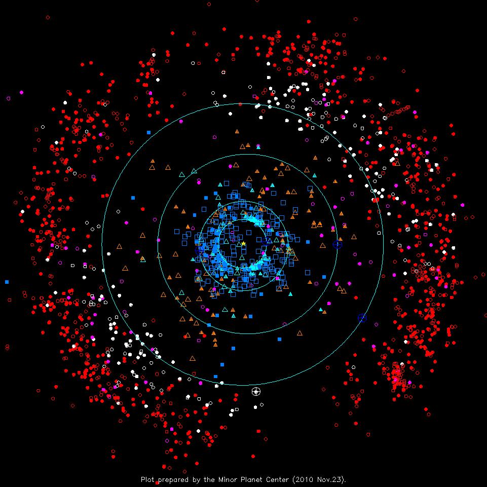
4
5 Wm. Robert Johnston

6
7

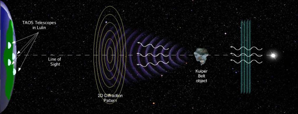
8 Fast photometry Many stars Multi-telescopes Perfect diffraction
")
9 TAOS(2005) (Photo by SK, Feb. 2004)
10 Some Statistics 5Hz observation with 110ms exposures from 2005 with 3 telescopes 4 telescopes operation from August star hours of data accumulated 2.7x10 10 flux measurement More than 30 TB raw images accumulated No occultation event found!
11 Upper limits set from TAOS data
12 TAOS 1 vs TAOS 2 Design TAOS 1 TAOS 2 F R Observable nights 50nts/yr 250nts/yr 5 Aperture 0.5m 1.3m 6.2 Background 16e- 2e Exposure time 105ms 50ms 0.47 Detection limits 2 km 0.7km 2 Field of view 1.7 o x1.7 o 1.7 o φ Total >100 The limiting magnitude will be 4 mag fainter to get 10x more stars.
13
 will be 154-mm in diameter (1.7-degrees).")
14 TAOS 2 telescope 1.3 m f/4 system 39.8 arc sec/mm The fully shielded and unvignetted field of view (FOV) will be 154-mm in diameter (1.7-degrees). The energy concentration will be 80% of incident light to fall within 1.0 arc second diameter.
15 Camera for TAOS 2 Basic requirements: 20Hz sampling 10~16 micron pixels (0.4 ~0.64 ) Cover 1.7 degree field, 2.27 square degrees Readout noise limited, read noise should be as low as possible Dark level < 0.1 e-/frame Preferable feature Different sampling rate for different stars Possibility to read the whole frame very few minutes

16 Current TAOS camera 5Hz sampling with 1MHz output rate Zipper mode readout Shutter kept open Read certain rows each time Sky stacked Streaks during row shifting
17 Possible sensor for TAOS 2 CCD based device > 20MHz/ch pixel rate Low noise required Frame transfer needed 200M pixels to be read in each frame Selective read electronics needed CMOS based device 70 windows in each 1k x 1k region Fast programmable windows needed (<0.5ms window switching time) Reasonable data rate
18 Possible TAOS 2 sensor EMCCD from e2v 20 MHz readout with <2e - read noise Frame transfer buffer Custom chip needed for large array Excess noise for bright stars Hybrid CMOS from Teledyne 2k x 2k with 18 microns CDS noise around 20 1MHz Window mode with single output Both options are very expensive!
19 Is monolithic CMOS the solution?
20 CMOS sensor we need Format : > 2K x 2K Pixel size : 10~16 microns QE : > 80% from 500~750nm Read noise : < 2e- Full well : > 60000e- Window switching time : < 0.5ms Total pixel rate : > 20Mpixel/s Dark rate : < 1e-/s Non destructive read mode supported
21 Commercial CMOS sensor CANON 50D CANON 5D QSI532 Effective sensor size 22.3 mm x 14.9 mm 35.8 mm x 23.9 mm 14.9 mm x 10.3 mm Pixel number Pixel size Data coding ISO 400 Readout noise Thermal 22 C 4752 x microns 4368 x microns 2184 x microns 14 bits 12 bits 16 bits 0.57 e- /ADU ADU (2.7 e-) 3.99 e- /ADU 3.77 ADU (3.8 e-) 1.31 e- /ADU 0.06 e-/sec 0.63 e-/sec - - Full well e e e- Dynamic range Christian Buil
22 CMOS Sarnoff Led by Jim Janesick CfA supported the study for x-ray sensors 3T, 5T and 6T structure studied More than 5 shuttle runs and Jazz semiconductor

23 Issues studied in prototypes Sensitivity Noise Full well Quantum efficiency Thermal current CCE, CTE On chip CDS Radiation damages Details refers to Paper series in SPIE proceeding 6276, 6295, 6690, 7439, 7742 by Jim Janesick Fundamental performance differences between CMOS and CCD imagers


24 BIG MIN I 1536 x 1536 x 8 um 5T pinned photo diode (PPD)

25 BIG MIN II 1024x micron pixels Improved buried channel MOSFET Window read by addressing each row and read certain columns. To be delivered this month Meet the lowest TAOS specs


26 SoloHI sensor Solar Orbiter Heliospheric Imager on board of ESA Solar Orbiter mission 4k x4k 10 micron device
27 Development issues Non destructive read: not possible for current 5T structure Full well: better to have > e- Package: backside illumination and small footprint for closely packed focal plane Foundry service: large format prototype requires stitching capability
28 Our Plan Single chip camera completed this summer Readout system build by John Geary (CfA) with BIG MIN II array Multi-chip camera with BIG MIN II in one year Development of TAOS custom array SoLoHI array to be the backup choice Alternatives from e2v and Canon First full camera within two years Good chance to get local industry involved in the development
TAOS II: Three 88-Megapixel astronomy arrays of large area, backthinned, and low-noise CMOS sensors
 TAOS II: Three 88-Megapixel astronomy arrays of large area, backthinned, and low-noise CMOS sensors CMOS Image Sensors for High Performance Applications TOULOUSE WORKSHOP - 26th & 27th NOVEMBER 2013 Jérôme
Detectors that cover a dynamic range of more than 1 million in several dimensions
 Detectors that cover a dynamic range of more than 1 million in several dimensions Detectors for Astronomy Workshop Garching, Germany 10 October 2009 James W. Beletic Teledyne Providing the best images
Characteristic of e2v CMOS Sensors for Astronomical Applications
 Characteristic of e2v CMOS Sensors for Astronomical Applications Shiang-Yu Wang* a, Hung-Hsu Ling a, Yen-Sang Hu a, John C. Geary b, Stephen M. Amato b, Jerome Pratlong c, Andrew Pike c, Paul Jorden c
Laboratory, University of Arizona, Tucson, AZ 85721; c ImagerLabs, 1995 S. Myrtle Ave., Monrovia CA INTRODUCTION ABSTRACT
 A CMOS Visible Image Sensor with Non-Destructive Readout Capability Gary R. Sims* a, Gene Atlas c, Eric Christensen b, Roger W. Cover a, Stephen Larson b, Hans J. Meyer a, William V. Schempp a a Spectral
Characterisation of a CMOS Charge Transfer Device for TDI Imaging
 Preprint typeset in JINST style - HYPER VERSION Characterisation of a CMOS Charge Transfer Device for TDI Imaging J. Rushton a, A. Holland a, K. Stefanov a and F. Mayer b a Centre for Electronic Imaging,
Low temperature measurements of the large-area, backthinned, and lownoise TAOSII CMOS sensors
 Low temperature measurements of the large-area, backthinned, and lownoise TAOSII CMOS sensors Steven Johnson, Jérôme Pratlong, Amr Ibrahim, Paul Jerram, Paul Jorden (e2v technologies) Shiang-Yu Wang and
Astronomy 341 Fall 2012 Observational Astronomy Haverford College. CCD Terminology
 CCD Terminology Read noise An unavoidable pixel-to-pixel fluctuation in the number of electrons per pixel that occurs during chip readout. Typical values for read noise are ~ 10 or fewer electrons per
Light gathering Power: Magnification with eyepiece:
 Telescopes Light gathering Power: The amount of light that can be gathered by a telescope in a given amount of time: t 1 /t 2 = (D 2 /D 1 ) 2 The larger the diameter the smaller the amount of time. If
CFHT and Subaru Wide Field Camera
 CFHT and Subaru Wide Field Camera WIRCam and Beyond: OIR instrumentation plan of ASIAA Chi-Hung Yan Institute of Astronomy and Astrophysics, Academia Sinica Canada France Hawaii Telescope 3.6 m telescope
CCDS. Lesson I. Wednesday, August 29, 12
 CCDS Lesson I CCD OPERATION The predecessor of the CCD was a device called the BUCKET BRIGADE DEVICE developed at the Phillips Research Labs The BBD was an analog delay line, made up of capacitors such
Properties of a Detector
 Properties of a Detector Quantum Efficiency fraction of photons detected wavelength and spatially dependent Dynamic Range difference between lowest and highest measurable flux Linearity detection rate
Camera Selection Criteria. Richard Crisp May 25, 2011
 Camera Selection Criteria Richard Crisp rdcrisp@earthlink.net www.narrowbandimaging.com May 25, 2011 Size size considerations Key issues are matching the pixel size to the expected spot size from the optical
CCD Characteristics Lab
 CCD Characteristics Lab Observational Astronomy 6/6/07 1 Introduction In this laboratory exercise, you will be using the Hirsch Observatory s CCD camera, a Santa Barbara Instruments Group (SBIG) ST-8E.
Detectors for microscopy - CCDs, APDs and PMTs. Antonia Göhler. Nov 2014
 Detectors for microscopy - CCDs, APDs and PMTs Antonia Göhler Nov 2014 Detectors/Sensors in general are devices that detect events or changes in quantities (intensities) and provide a corresponding output,
Charged Coupled Device (CCD) S.Vidhya
 S.Vidhya") Charged Coupled Device (CCD) S.Vidhya 02.04.2016 Sensor Physical phenomenon Sensor Measurement Output A sensor is a device that measures a physical quantity and converts it into a signal which can be read
Charged Coupled Device (CCD) S.Vidhya 02.04.2016 Sensor Physical phenomenon Sensor Measurement Output A sensor is a device that measures a physical quantity and converts it into a signal which can be read
Evaluation of large pixel CMOS image sensors for the Tomo-e Gozen wide field camera
 Evaluation of large pixel CMOS image sensors for the Tomo-e Gozen wide field camera Yuto Kojima (Univ. of Tokyo) S. Sako, R. Ohsawa, H. Takahashi, M. Doi, N. Kobayashi, and the Tomo-e Gozen project Canon
More Imaging Luc De Mey - CEO - CMOSIS SA
 More Imaging Luc De Mey - CEO - CMOSIS SA Annual Review / June 28, 2011 More Imaging CMOSIS: Vision & Mission CMOSIS s Business Concept On-Going R&D: More Imaging CMOSIS s Vision Image capture is a key
Acquisition. Some slides from: Yung-Yu Chuang (DigiVfx) Jan Neumann, Pat Hanrahan, Alexei Efros
 Jan Neumann, Pat Hanrahan, Alexei Efros") Acquisition Some slides from: Yung-Yu Chuang (DigiVfx) Jan Neumann, Pat Hanrahan, Alexei Efros Image Acquisition Digital Camera Film Outline Pinhole camera Lens Lens aberrations Exposure Sensors Noise
Acquisition Some slides from: Yung-Yu Chuang (DigiVfx) Jan Neumann, Pat Hanrahan, Alexei Efros Image Acquisition Digital Camera Film Outline Pinhole camera Lens Lens aberrations Exposure Sensors Noise
The Asteroid Finder Focal Plane
 The Asteroid Finder Focal Plane H. Michaelis (1), S. Mottola (1), E. Kührt (1), T. Behnke (1), G. Messina (1), M. Solbrig (1), M. Tschentscher (1), N. Schmitz (1), K. Scheibe (2), J. Schubert (3), M. Hartl
Based on lectures by Bernhard Brandl
 Astronomische Waarneemtechnieken (Astronomical Observing Techniques) Based on lectures by Bernhard Brandl Lecture 10: Detectors 2 1. CCD Operation 2. CCD Data Reduction 3. CMOS devices 4. IR Arrays 5.
CMOS Today & Tomorrow
 CMOS Today & Tomorrow Uwe Pulsfort TDALSA Product & Application Support Overview Image Sensor Technology Today Typical Architectures Pixel, ADCs & Data Path Image Quality Image Sensor Technology Tomorrow
ASTROPHOTOGRAPHY (What is all the noise about?) Chris Woodhouse ARPS FRAS
 Chris Woodhouse ARPS FRAS") ASTROPHOTOGRAPHY (What is all the noise about?) Chris Woodhouse ARPS FRAS Havering Astronomical Society a bit about me living on the edge what is noise? break noise combat strategies cameras and sensors
ASTROPHOTOGRAPHY (What is all the noise about?) Chris Woodhouse ARPS FRAS Havering Astronomical Society a bit about me living on the edge what is noise? break noise combat strategies cameras and sensors
The Simbol-X. Low Energy Detector. Peter Lechner PNSensor & MPI-HLL. on behalf of the LED consortium. Paris, Simbol-X Symposium. P.
 The Simbol-X Low Energy Detector Peter Lechner PNSensor & MPI-HLL on behalf of the LED consortium Simbol-X X Symposium 1 LED collaboration K. Heinzinger,, G. Lutz, G. Segneri, H. Soltau PNSensor GmbH &
Astronomical Detectors. Lecture 3 Astronomy & Astrophysics Fall 2011
 Astronomical Detectors Lecture 3 Astronomy & Astrophysics Fall 2011 Detector Requirements Record incident photons that have been captured by the telescope. Intensity, Phase, Frequency, Polarization Difficulty
Simulation of High Resistivity (CMOS) Pixels
 Pixels") Simulation of High Resistivity (CMOS) Pixels Stefan Lauxtermann, Kadri Vural Sensor Creations Inc. AIDA-2020 CMOS Simulation Workshop May 13 th 2016 OUTLINE 1. Definition of High Resistivity Pixel Also
Simulation of High Resistivity (CMOS) Pixels Stefan Lauxtermann, Kadri Vural Sensor Creations Inc. AIDA-2020 CMOS Simulation Workshop May 13 th 2016 OUTLINE 1. Definition of High Resistivity Pixel Also
Jan Bogaerts imec
 imec 2007 1 Radiometric Performance Enhancement of APS 3 rd Microelectronic Presentation Days, Estec, March 7-8, 2007 Outline Introduction Backside illuminated APS detector Approach CMOS APS (readout)
Compatible with Windows 8/7/XP, and Linux; Universal programming interfaces for easy custom programming.
 NIRvana: 640LN The NIRvana: 640LN from Princeton Instruments is a scientific-grade, deep-cooled, large format InGaAs camera for low-light scientific SWIR imaging and spectroscopy applications. The camera
STA1600LN x Element Image Area CCD Image Sensor
 ST600LN 10560 x 10560 Element Image Area CCD Image Sensor FEATURES 10560 x 10560 Photosite Full Frame CCD Array 9 m x 9 m Pixel 95.04mm x 95.04mm Image Area 100% Fill Factor Readout Noise 2e- at 50kHz
Charge-Coupled Device (CCD) Detectors pixel silicon chip electronics cryogenics
 Detectors pixel silicon chip electronics cryogenics") Charge-Coupled Device (CCD) Detectors As revolutionary in astronomy as the invention of the telescope and photography semiconductor detectors a collection of miniature photodiodes, each called a picture
Charge-Coupled Device (CCD) Detectors As revolutionary in astronomy as the invention of the telescope and photography semiconductor detectors a collection of miniature photodiodes, each called a picture
Corner Rafts LSST Camera Workshop SLAC Sept 19, 2008
 Corner Rafts LSST Camera Workshop SLAC Sept 19, 2008 Scot Olivier LLNL 1 LSST Conceptual Design Review 2 Corner Raft Session Agenda 1. System Engineering 1. Tolerance analysis 2. Requirements flow-down
What an Observational Astronomer needs to know!
 What an Observational Astronomer needs to know! IRAF:Photometry D. Hatzidimitriou Masters course on Methods of Observations and Analysis in Astronomy Basic concepts Counts how are they related to the actual
ISIS2 as a Pixel Sensor for ILC
 ISIS2 as a Pixel Sensor for ILC Yiming Li (University of Oxford) on behalf of UK ISIS Collaboration (U. Oxford, RAL, Open University) LCWS 10 Beijing, 28th March 2010 1 / 24 Content Introduction to ISIS
CCD Requirements for Digital Photography
 IS&T's 2 PICS Conference IS&T's 2 PICS Conference Copyright 2, IS&T CCD Requirements for Digital Photography Richard L. Baer Hewlett-Packard Laboratories Palo Alto, California Abstract The performance
European Low Flux CMOS Image Sensor
 European Low Flux CMOS Image Sensor Description and Preliminary Results Ajit Kumar Kalgi 1, Wei Wang 1, Bart Dierickx 1, Dirk Van Aken 1, Kaiyuan Wu 1, Alexander Klekachev 1, Gerlinde Ruttens 1, Kyriaki
TELEDYNE S HIGH PERFORMANCE INFRARED DETECTORS FOR SPACE MISSIONS. Paul Jerram and James Beletic ICSO October 2018
 TELEDYNE S HIGH PERFORMANCE INFRARED DETECTORS FOR SPACE MISSIONS Paul Jerram and James Beletic ICSO October 2018 Teledyne High Performance Image Sensors Teledyne DALSA Waterloo, Ontario (Design, I&T)
THE CCD RIDDLE REVISTED: SIGNAL VERSUS TIME LINEAR SIGNAL VERSUS VARIANCE NON-LINEAR
 THE CCD RIDDLE REVISTED: SIGNAL VERSUS TIME LINEAR SIGNAL VERSUS VARIANCE NON-LINEAR Mark Downing 1, Peter Sinclaire 1. 1 ESO, Karl Schwartzschild Strasse-2, 85748 Munich, Germany. ABSTRACT The photon
Selecting an image sensor for the EJSM VIS/NIR camera systems
 Selecting an image sensor for the EJSM VIS/NIR camera systems presented by Harald Michaelis (DLR-PF) Folie 1 EJSM- Jan. 18th 2010; ESTEC What for a detector/sensor we shall chose for EJSM? Vortragstitel
ABSTRACT. Supported by U.S. DoE grant No. DE-FG02-96ER54375
 ABSTRACT A CCD imaging system is currently being developed for T e (,t) and bolometric measurements on the Pegasus Toroidal Experiment. Soft X-rays (E
ACTIVE PIXEL SENSORS VS. CHARGE-COUPLED DEVICES
 ACTIVE PIXEL SENSORS VS. CHARGE-COUPLED DEVICES Dr. Eric R. Fossum Imaging Systems Section Jet Propulsion Laboratory, California Institute of Technology (818) 354-3128 1993 IEEE Workshop on CCDs and Advanced
Fundamentals of CMOS Image Sensors
 CHAPTER 2 Fundamentals of CMOS Image Sensors Mixed-Signal IC Design for Image Sensor 2-1 Outline Photoelectric Effect Photodetectors CMOS Image Sensor(CIS) Array Architecture CIS Peripherals Design Considerations
Factors Affecting Pixel Scaling Limits for cellphone imaging systems
 Factors Affecting Pixel Scaling Limits for cellphone imaging systems October 28, 2010 Richard Crisp rcrisp@narrowbandimaging.com Agenda Pixel Scaling Limits Optical Considerations Image Sensor Considerations
Last class. This class. CCDs Fancy CCDs. Camera specs scmos
 CCDs and scmos Last class CCDs Fancy CCDs This class Camera specs scmos Fancy CCD cameras: -Back thinned -> higher QE -Unexposed chip -> frame transfer -Electron multiplying -> higher SNR -Fancy ADC ->
Digital camera. Sensor. Memory card. Circuit board
 Digital camera Circuit board Memory card Sensor Detector element (pixel). Typical size: 2-5 m square Typical number: 5-20M Pixel = Photogate Photon + Thin film electrode (semi-transparent) Depletion volume
Abstract. Preface. Acknowledgments
 Contents Abstract Preface Acknowledgments iv v vii 1 Introduction 1 1.1 A Very Brief History of Visible Detectors in Astronomy................ 1 1.2 The CCD: Astronomy s Champion Workhorse......................
CCD and CMOS Imaging Devices for Large (Ground Based) Telescopes. Veljko Radeka BNL SNIC April 3, 2006
 Telescopes. Veljko Radeka BNL SNIC April 3, 2006") CCD and CMOS Imaging Devices for Large (Ground Based) Telescopes Veljko Radeka BNL SNIC April 3, 2006 1 Large Telescopes Survey telescope Deep probe Primary Mirror dia.=d m, Area= A Large (~8m) Very large
CCD and CMOS Imaging Devices for Large (Ground Based) Telescopes Veljko Radeka BNL SNIC April 3, 2006 1 Large Telescopes Survey telescope Deep probe Primary Mirror dia.=d m, Area= A Large (~8m) Very large
Open Research Online The Open University s repository of research publications and other research outputs
 Open Research Online The Open University s repository of research publications and other research outputs PSF and non-uniformity in a monolithic, fully depleted, 4T CMOS image sensor Conference or Workshop
PRELIMINARY. CCD 3041 Back-Illuminated 2K x 2K Full Frame CCD Image Sensor FEATURES
 CCD 3041 Back-Illuminated 2K x 2K Full Frame CCD Image Sensor FEATURES 2048 x 2048 Full Frame CCD 15 µm x 15 µm Pixel 30.72 mm x 30.72 mm Image Area 100% Fill Factor Back Illuminated Multi-Pinned Phase
Introduction. Chapter 1
 1 Chapter 1 Introduction During the last decade, imaging with semiconductor devices has been continuously replacing conventional photography in many areas. Among all the image sensors, the charge-coupled-device
Electron Multiplying CCDs
 SNIC Symposium, Stanford, California 3-6 April 2006 Electron Multiplying CCDs P.A.Jerram, P. J. Pool, D. J. Burt, R. T. Bell, M.S.Robbins e2v technologies ltd, 106, Waterhouse Lane, Chelmsford, Essex,
High Resolution 640 x um Pitch InSb Detector
 High Resolution 640 x 512 15um Pitch InSb Detector Chen-Sheng Huang, Bei-Rong Chang, Chien-Te Ku, Yau-Tang Gau, Ping-Kuo Weng* Materials & Electro-Optics Division National Chung Shang Institute of Science
Detectors for AXIS. Eric D. Miller Catherine Grant (MIT)
") Detectors for AXIS Eric D. Miller Catherine Grant (MIT) Outline detector technology and capabilities CCD (charge coupled device) APS (active pixel sensor) notional AXIS detector background particle environment
Detectors for AXIS Eric D. Miller Catherine Grant (MIT) Outline detector technology and capabilities CCD (charge coupled device) APS (active pixel sensor) notional AXIS detector background particle environment
Infrared detectors for wavefront sensing
 Infrared detectors for wavefront sensing Jean-Luc Gach et al. The project has received funding from the European Union's Horizon 2020 research and innovation programme under grant agreement No 673944 First
The new CMOS Tracking Camera used at the Zimmerwald Observatory
 13-0421 The new CMOS Tracking Camera used at the Zimmerwald Observatory M. Ploner, P. Lauber, M. Prohaska, P. Schlatter, J. Utzinger, T. Schildknecht, A. Jaeggi Astronomical Institute, University of Bern,
Padova and Asiago Observatories
 ISSN 1594-1906 Padova and Asiago Observatories The Echelle E2V CCD47-10 CCD H. Navasardyan, M. D'Alessandro, E. Giro, Technical Report n. 22 September 2004 Document available at: http://www.pd.astro.it/
Selecting the NIR detectors for Euclid
 National Aeronautics and Space Administration Jet Propulsion Laboratory California Institute of Technology Selecting the NIR detectors for Euclid Stefanie Wachter Michael Seiffert On behalf of the Euclid
OPAL Optical Profiling of the Atmospheric Limb
 OPAL Optical Profiling of the Atmospheric Limb Alan Marchant Chad Fish Erik Stromberg Charles Swenson Jim Peterson OPAL STEADE Mission Storm Time Energy & Dynamics Explorers NASA Mission of Opportunity
IT FR R TDI CCD Image Sensor
 4k x 4k CCD sensor 4150 User manual v1.0 dtd. August 31, 2015 IT FR 08192 00 R TDI CCD Image Sensor Description: With the IT FR 08192 00 R sensor ANDANTA GmbH builds on and expands its line of proprietary
High-end CMOS Active Pixel Sensor for Hyperspectral Imaging
 R11 High-end CMOS Active Pixel Sensor for Hyperspectral Imaging J. Bogaerts (1), B. Dierickx (1), P. De Moor (2), D. Sabuncuoglu Tezcan (2), K. De Munck (2), C. Van Hoof (2) (1) Cypress FillFactory, Schaliënhoevedreef
IRIS3 Visual Monitoring Camera on a chip
 IRIS3 Visual Monitoring Camera on a chip ESTEC contract 13716/99/NL/FM(SC) G.Meynants, J.Bogaerts, W.Ogiers FillFactory, Mechelen (B) T.Cronje, T.Torfs, C.Van Hoof IMEC, Leuven (B) Microelectronics Presentation
Electron Multiplying Charge Coupled Devices. Craig Mackay, Institute of Astronomy, University of Cambridge.
 Electron Multiplying Charge Coupled Devices Craig Mackay, Institute of Astronomy, University of Cambridge. Outline Introduction to EMCCDs: General Characteristics Applications of EMCCDs: Current and Potential
Two-phase full-frame CCD with double ITO gate structure for increased sensitivity
 Two-phase full-frame CCD with double ITO gate structure for increased sensitivity William Des Jardin, Steve Kosman, Neal Kurfiss, James Johnson, David Losee, Gloria Putnam *, Anthony Tanbakuchi (Eastman
Wide-field Infrared Survey Explorer (WISE)
") Wide-field Infrared Survey Explorer (WISE) Latent Image Characterization Version 1.0 12-July-2009 Prepared by: Deborah Padgett Infrared Processing and Analysis Center California Institute of Technology
Wide-field Infrared Survey Explorer (WISE) Latent Image Characterization Version 1.0 12-July-2009 Prepared by: Deborah Padgett Infrared Processing and Analysis Center California Institute of Technology
Fully depleted, thick, monolithic CMOS pixels with high quantum efficiency
 Fully depleted, thick, monolithic CMOS pixels with high quantum efficiency Andrew Clarke a*, Konstantin Stefanov a, Nicholas Johnston a and Andrew Holland a a Centre for Electronic Imaging, The Open University,
ARRAY CONTROLLER REQUIREMENTS
 ARRAY CONTROLLER REQUIREMENTS TABLE OF CONTENTS 1 INTRODUCTION...3 1.1 QUANTUM EFFICIENCY (QE)...3 1.2 READ NOISE...3 1.3 DARK CURRENT...3 1.4 BIAS STABILITY...3 1.5 RESIDUAL IMAGE AND PERSISTENCE...4
Presented by Jerry Hubbell Lake of the Woods Observatory (MPC I24) President, Rappahannock Astronomy Club
 President, Rappahannock Astronomy Club") Presented by Jerry Hubbell Lake of the Woods Observatory (MPC I24) President, Rappahannock Astronomy Club ENGINEERING A FIBER-FED FED SPECTROMETER FOR ASTRONOMICAL USE Objectives Discuss the engineering
Presented by Jerry Hubbell Lake of the Woods Observatory (MPC I24) President, Rappahannock Astronomy Club ENGINEERING A FIBER-FED FED SPECTROMETER FOR ASTRONOMICAL USE Objectives Discuss the engineering
A Quadrant-CCD star tracker
 A Quadrant-CCD star tracker M. Clampin, S. T. Durrance, R. Barkhouser, D. A. Golimowski, A. Wald and W. G. Fastie Centre for Astrophysical Sciences, The Johns Hopkins University, Baltimore, MD21218. D.L
CCD1600A Full Frame CCD Image Sensor x Element Image Area
 - 1 - General Description CCD1600A Full Frame CCD Image Sensor 10560 x 10560 Element Image Area General Description The CCD1600 is a 10560 x 10560 image element solid state Charge Coupled Device (CCD)
Interpixel crosstalk in a 3D-integrated active pixel sensor for x-ray detection
 Interpixel crosstalk in a 3D-integrated active pixel sensor for x-ray detection The MIT Faculty has made this article openly available. Please share how this access benefits you. Your story matters. Citation
Charge coupled CMOS and hybrid detector arrays
 Charge coupled CMOS and hybrid detector arrays James Janesick Sarnoff Corporation, 4952 Warner Ave., Suite 300, Huntington Beach, CA. 92649 Headquarters: CN5300, 201 Washington Road Princeton, NJ 08543-5300
Using Machine Vision Cameras for Solar Imaging. Dr Stuart Green
 Using Machine Vision Cameras for Solar Imaging Dr Stuart Green Hubble Ultra-deep Field Image Estimated 100 billion galaxies in the observable universe Estimated 200-400 billion stars in our own galaxy
XMM OM Serendipitous Source Survey Catalogue (XMM-SUSS2.1)
") XMM OM Serendipitous Source Survey Catalogue (XMM-SUSS2.1) 1 Introduction The second release of the XMM OM Serendipitous Source Survey Catalogue (XMM-SUSS2) was produced by processing the XMM-Newton Optical
XMM OM Serendipitous Source Survey Catalogue (XMM-SUSS2.1) 1 Introduction The second release of the XMM OM Serendipitous Source Survey Catalogue (XMM-SUSS2) was produced by processing the XMM-Newton Optical
Low Cost Earth Sensor based on Oxygen Airglow
 Assessment Executive Summary Date : 16.06.2008 Page: 1 of 7 Low Cost Earth Sensor based on Oxygen Airglow Executive Summary Prepared by: H. Shea EPFL LMTS herbert.shea@epfl.ch EPFL Lausanne Switzerland
Camera Test Protocol. Introduction TABLE OF CONTENTS. Camera Test Protocol Technical Note Technical Note
 Technical Note CMOS, EMCCD AND CCD CAMERAS FOR LIFE SCIENCES Camera Test Protocol Introduction The detector is one of the most important components of any microscope system. Accurate detector readings
CMOS Imagers : Today and Tomorrow
 CMOS Imagers : Today and Tomorrow IISW2015 Highlights Albert Theuwissen Harvest Imaging (B) Image Capturing Circle the Netherlands Belgium Harvest Imaging Germany France copyright 2010 Albert Theuwissen
CCDs for Earth Observation James Endicott 1 st September th UK China Workshop on Space Science and Technology, Milton Keynes, UK
 CCDs for Earth Observation James Endicott 1 st September 2011 7 th UK China Workshop on Space Science and Technology, Milton Keynes, UK Introduction What is this talk all about? e2v sensors in spectrometers
Dynamic Range. Can I look at bright and faint things at the same time?
 Detector Basics The purpose of any detector is to record the light collected by the telescope. All detectors transform the incident radiation into a some other form to create a permanent record, such as
AstraLux SNR and DR considerations
 AstraLux SNR page 1 AstraLux SNR and DR considerations Stefan Hippler, hippler@mpia.de, March 2008 AstraLux Homepage: http://www.mpia.de/astralux Contents 1 Signal to Noise (SNR) considerations for AstraLux
TIRCAM2 (TIFR Near Infrared Imaging Camera - 3.6m Devasthal Optical Telescope (DOT)
") TIRCAM2 (TIFR Near Infrared Imaging Camera - II) @ 3.6m Devasthal Optical Telescope (DOT) (ver 4.0 June 2017) TIRCAM2 (TIFR Near Infrared Imaging Camera - II) is a closed cycle cooled imager that has been
TIRCAM2 (TIFR Near Infrared Imaging Camera - II) @ 3.6m Devasthal Optical Telescope (DOT) (ver 4.0 June 2017) TIRCAM2 (TIFR Near Infrared Imaging Camera - II) is a closed cycle cooled imager that has been
The 0.84 m Telescope OAN/SPM - BC, Mexico
 The 0.84 m Telescope OAN/SPM - BC, Mexico Readout error CCD zero-level (bias) ramping CCD bias frame banding Shutter failure Significant dark current Image malting Focus frame taken during twilight IR
CHARGE-COUPLED DEVICE (CCD)
") CHARGE-COUPLED DEVICE (CCD) Definition A charge-coupled device (CCD) is an analog shift register, enabling analog signals, usually light, manipulation - for example, conversion into a digital value that
CHARGE-COUPLED DEVICE (CCD) Definition A charge-coupled device (CCD) is an analog shift register, enabling analog signals, usually light, manipulation - for example, conversion into a digital value that
Science Detectors for E-ELT Instruments. Mark Casali
 Science Detectors for E-ELT Instruments Mark Casali 1 The Telescope Nasmyth telescope with a segmented primary mirror. Novel 5 mirror design to include adaptive optics in the telescope. Classical 3mirror
ABSTRACT. Section I Overview of the µdss
 An Autonomous Low Power High Resolution micro-digital Sun Sensor Ning Xie 1, Albert J.P. Theuwissen 1, 2 1. Delft University of Technology, Delft, the Netherlands; 2. Harvest Imaging, Bree, Belgium; ABSTRACT
ABSTRACT 1. INTRODUCTION
 Teledyne s High Performance Infrared Detectors for Space Missions Paul Jerram a and James Beletic b a Teledyne e2v Space Imaging, Chelmsford, UK, CM7 4BS b Teledyne Imaging Sensors, Camarillo, California,
Integrated Multi-Aperture Imaging
 Integrated Multi-Aperture Imaging Keith Fife, Abbas El Gamal, Philip Wong Department of Electrical Engineering, Stanford University, Stanford, CA 94305 1 Camera History 2 Camera History Despite progress,
Minimizes reflection losses from UV to IR; No optical losses due to multiple optical surfaces; Optional AR coating and wedge windows available.
 SOPHIA: 2048B The SOPHIA : 2048B camera from Princeton Instruments (PI) is fully integrated, ultra-low noise 2048 x 2048, 15 µm pixel CCD camera designed expressly for the most demanding quantitative scientific
Colorado School of Mines. Computer Vision. Professor William Hoff Dept of Electrical Engineering &Computer Science.
 Professor William Hoff Dept of Electrical Engineering &Computer Science http://inside.mines.edu/~whoff/ 1 Sensors and Image Formation Imaging sensors and models of image formation Coordinate systems Digital
Coronal and heliospheric imaging instrumentation development at RAL Space
 Coronal and heliospheric imaging instrumentation development at RAL Space JA Davies, CJ Eyles, DK Griffin, RA Harrison, KF Middleton, AG Richards, JK Rogers, SJ Tappin, IAJ Tosh, NR Waltham Heritage (1)
ABSTRACT. Keywords: 0,18 micron, CMOS, APS, Sunsensor, Microned, TNO, TU-Delft, Radiation tolerant, Low noise. 1. IMAGERS FOR SPACE APPLICATIONS.
 Active pixel sensors: the sensor of choice for future space applications Johan Leijtens(), Albert Theuwissen(), Padmakumar R. Rao(), Xinyang Wang(), Ning Xie() () TNO Science and Industry, Postbus, AD
Photometry of the variable stars using CCD detectors
 Contrib. Astron. Obs. Skalnaté Pleso 35, 35 44, (2005) Photometry of the variable stars using CCD detectors I. Photometric reduction. Š. Parimucha 1, M. Vaňko 2 1 Institute of Physics, Faculty of Natural
Where detectors are used in science & technology
 Lecture 9 Outline Role of detectors Photomultiplier tubes (photoemission) Modulation transfer function Photoconductive detector physics Detector architecture Where detectors are used in science & technology
Lecture 30: Image Sensors (Cont) Computer Graphics and Imaging UC Berkeley CS184/284A
 Computer Graphics and Imaging UC Berkeley CS184/284A") Lecture 30: Image Sensors (Cont) Computer Graphics and Imaging UC Berkeley Reminder: The Pixel Stack Microlens array Color Filter Anti-Reflection Coating Stack height 4um is typical Pixel size 2um is typical
Lecture 30: Image Sensors (Cont) Computer Graphics and Imaging UC Berkeley Reminder: The Pixel Stack Microlens array Color Filter Anti-Reflection Coating Stack height 4um is typical Pixel size 2um is typical
Specifications Summary 1. Array Size (pixels) Pixel Size. Sensor Size. Pixel Well Depth (typical) 95,000 e - 89,000 e -
 Pixel Size. Sensor Size. Pixel Well Depth (typical) 95,000 e - 89,000 e -") Apogee Alta Series System Features 1 High Resolution Sensor 1.0 Megapixel sensor with 13 mm pixels delivers a large field of view with high resolution. Programmable TE cooling down to 50 o C below ambient
Apogee Alta Series System Features 1 High Resolution Sensor 1.0 Megapixel sensor with 13 mm pixels delivers a large field of view with high resolution. Programmable TE cooling down to 50 o C below ambient
A 3D Multi-Aperture Image Sensor Architecture
 A 3D Multi-Aperture Image Sensor Architecture Keith Fife, Abbas El Gamal and H.-S. Philip Wong Department of Electrical Engineering Stanford University Outline Multi-Aperture system overview Sensor architecture
DV420 SPECTROSCOPY. issue 2 rev 1 page 1 of 5m. associated with LN2
 SPECTROSCOPY Andor s DV420 CCD cameras offer the best price/performance for a wide range of spectroscopy applications. The 1024 x 256 array with 26µm 2 pixels offers the best dynamic range versus resolution.
Radiometric Solar Telescope (RaST) The case for a Radiometric Solar Imager,
 The case for a Radiometric Solar Imager,") SORCE Science Meeting 29 January 2014 Mark Rast Laboratory for Atmospheric and Space Physics University of Colorado, Boulder Radiometric Solar Telescope (RaST) The case for a Radiometric Solar Imager,
SORCE Science Meeting 29 January 2014 Mark Rast Laboratory for Atmospheric and Space Physics University of Colorado, Boulder Radiometric Solar Telescope (RaST) The case for a Radiometric Solar Imager,
Charged-Coupled Devices
 Charged-Coupled Devices Charged-Coupled Devices Useful texts: Handbook of CCD Astronomy Steve Howell- Chapters 2, 3, 4.4 Measuring the Universe George Rieke - 3.1-3.3, 3.6 CCDs CCDs were invented in 1969
Observational Astronomy
 Observational Astronomy Instruments The telescope- instruments combination forms a tightly coupled system: Telescope = collecting photons and forming an image Instruments = registering and analyzing the
Design and Performance of a Pinned Photodiode CMOS Image Sensor Using Reverse Substrate Bias
 Design and Performance of a Pinned Photodiode CMOS Image Sensor Using Reverse Substrate Bias 13 September 2017 Konstantin Stefanov Contents Background Goals and objectives Overview of the work carried
High Performance SWIR HgCdTe 320x256/30µm FPAs at Teledyne Judson Technologies
 High Performance SWIR HgCdTe 320x256/30µm FPAs at Teledyne Judson Technologies Henry Yuan, Jiawen Zhang, Jongwoo Kim, Carl Meyer, Joyce Laquindanum, Joe Kimchi, JihFen Lei 221 Commerce Drive, Montgomeryville,
Astro-photography. Daguerreotype: on a copper plate
 AST 1022L Astro-photography 1840-1980s: Photographic plates were astronomers' main imaging tool At right: first ever picture of the full moon, by John William Draper (1840) Daguerreotype: exposure using