Scanning Probe Microscope SPM-9700 C147-E011A
|
|
|
- Pearl Green
- 6 years ago
- Views:
Transcription


1 Scanning Probe Microscope C147-E011A


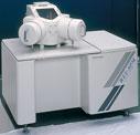
2 Making the Unknown Visible Scanning probe microscope (SPM) is a generic term for microscopes that scan sample surfaces with an extremely sharp probe to observe their three-dimensional image or local properties at high magnifications. The offers higher performance, faster speeds, and easier operation.


3 Functionality and Expandability to Meet a Wide Variety of Requirements P. 4 Head-Slide Mechanism High Stability P. 6 Head-Slide Mechanism High Throughput P. 7 Ease of Operation Minimizes Distraction from Observation to Analysis P. 8 Wide Variety of 3D Rendering Functions Using Mouse Operations P. 10 Particle Analysis Software P. 11 SPM Data Room Website P. 12 SPM Unit P. 14 WET-SPM Series P. 16 WET-SPM Series Options Specifications P. 18 P. 20 Installation Specifications P. 21


4 Functionality and Expandability to Meet a Wide Range of Requirements indicates standard specification. indicates optional specification. Other special orders are also accepted. For more information, contact your Shimadzu representative. Contact Mode Dynamic Mode Phase Mode Lateral Force (LFM) Mode Force Modulation Mode Current Mode, I/V Surface Potential (KFM) Mode Magnetic Force (MFM) Mode Force Curve Force Mapping (special order) Vector Scanning (special order) Adhesion layer Sample N S N S 4


5 Standard Scanner Unit Wide Range Scanner Unit 125 Deep-Type Scanner Unit Z13 Narrow N Range Scanner Unit Petri Dish Type Solution on Cell Electrochemical Solution Cell High Magnification Optical Microscope Unit Optical Microscope Unit with CCD Optical Microscope Unit Fiber Light Particle Analysis Software Desk-Type Air-Spring Vibration Damper Active Vibration Damper Computer Table Static Eliminator Environment Controlled Chamber CH-II (without TMP) Environment Controlled Chamber CH-III (with TMP) Sample Heating Unit Light Irradiation Unit Temperature and Humidity Controller Sample Heating and Cooling Unit Gas Spray Unit 5
6


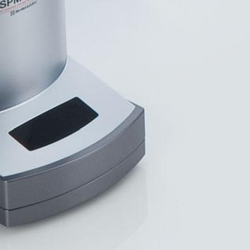
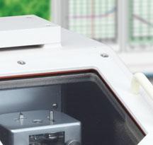
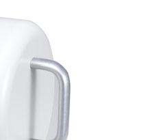
7 Head-Slide Mechanism High Stability Allows Sliding the Entire Optical Lever System as a Single Unit, While Maintaining High Rigidity. The laser remains stable and irradiates the cantilever even while replacing samples. Design is resistant to vibration, noise, wind, and other external disturbances, so a specialized enclosure is not necessary. The main unit includes a built-in vibration isolator. Right Side View (actual size) Sample Secret to the High Stability of the Remarkable Mechanism Maintains High Performance Comparison of Stability for Different Laser Irradiation Laser Irradiated Continuously a.u. Initial stabilization Replace sample Replace sample Replace sample Replace sample Replace sample System Without Head-Slide Mechanism (one example) a.u. Laser Irradiated Intermittently Initial stabilization Remove holder Replace sample Install holder Adjust optical axis Remove holder Replace sample Install holder Adjust optical axis 6

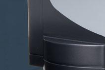
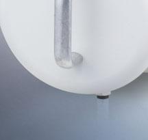
8 Head-Slide Mechanism High Throughput Successfully Opened Up the Area Around the Sample While Maintaining High Rigidity Samples can be replaced without removing the cantilever holder. Samples can be accessed even during SPM observation. Samples are approached automatically, regardless of thesample thickness. (Japanese Patent No ) Left Side View (actual size) Sample Secret to the High Throughput of the Remarkable Mechanism Optimized for Ease of Operation Comparison of Throughput for Differences in Replacing Samples Samples Replaced by Sliding the Head Slide head Replace sample Slide head back Set parameters Observe Save Switch to next sample Dramatically Faster System Without Head-Slide Mechanism (one example) Samples Replaced by Disassembling the Head Open enclosure Remove head screws Remove head Remove cantilever holder Replace sample Install cantilever holder Set up optical microscope Switch light ON while viewing via microscope Install head Fasten head screws Adjust optical axis Switch light OFF Adjust photodetector Remove optical microscope Close enclosure Wait for stabilization again Set parameters Observe Save Switch to next sample Scanning Probe Microscope 7
 provides borderless support for operations ranging from online")


9 Ease of Operation Minimizes Distraction from Observation to Analysis A revolutionary layout-free graphical user interface (GUI) provides borderless support for operations ranging from online observation to offline analysis. This means the SPM can be operated from observation to analysis without confusion. Guidance Area Observation Area Control Window Operate Without Confusion From startup to observation and analysis, the SPM can be operated using only mouse clicks; no complicated settings are required 1 Startup 2 Setup 3 Start Observation Select the observation mode in the manager window. Follow the steps indicated in the guidance window to easily complete setup. Clicking the [Observation Start] button performs all operations automatically, from approach to observation. 8


 The scanning direction, force between the probe and sample, or the applied")
10 Determine the Observation Position Without Confusion 1 Observation Window Up to 8 images can be displayed simultaneously. This means the surface shape and physical properties can be compared in multiple images, while scanning. 2 Navigator The Navigator allows freely navigating from a broad area to any specific area desired. Saved image data can be displayed as reference as well. Obtain Observation Results Without Confusion 3 Online Profile Cross-section profiles can be measured in the online window while observing samples. 4 Image History Past image data can be displayed next to current observation images for comparison. Wide Assortment of Scanning Functions 5 Force Mapping 6 Vector Scanning (special order) A force curve can be measured for each point in observed image data to acquire a distribution of sample mechanical properties or adhesion force. (special order) The scanning direction, force between the probe and sample, or the applied voltage can be programmed to allow scanning according to a program. Improved Usability! 4 Display 5 Image data observed in the past can be viewed without switching offline. Offline Analysis A wide selection of functions for displaying, processing, and analyzing images are available for expressing observation results more attractively and quantitatively. Scanning Probe Microscope 9


11 Wide Variety of 3D Rendering Functions Using Mouse Operations Use the mouse to freely rotate images, zoom, or change the Z-axis magnification. This enables expressing image data in a variety of ways while confirming the data in real time. Zoom Rotation Change Z-Axis Magnification Texture Function Height information can be displayed overlaid with information about other physical properties. This allows clearly showing the relationship between both parameters. 3D Cross-Section Profile Analysis Cross-section profiles can be analyzed in 3D images. If physical property information is expressed in terms of texture, respective cross-section profiles can be displayed and analyzed in the same location. 3D Image Overlay of Topographic Image and Phase Image 10


 Particle Extraction and Classification Results Histogram of Mean Radius E.")
12 Particle Analysis Software (option) The particle analysis software extracts multiple particles from image data and calculates feature values for each particle, then analyzes and displays them. This is especially useful for processing data statistically. The following wide selection of feature values and their corresponding statistical quantities can be calculated, tabulated, sorted, or graphed. Numerical data can be exported. Feature Parameters 1 Center X 2 Center Y 3 Maximum Diameter 4 Pattern Width 5 Horizontal Feret Length 6 Vertical Feret Length 7 Radius as Circle excluding Hole 8 Radius as Circle including Hole 9 Mean Radius 10 Mean Radius Variance 11 Nearest Distance 12 Perimeter 13 C Perimeter 14 Maximum Z 15 Minimum Z 16 Average Z 17 Average Round Z 18 Area excluding Holes 19 Area including Holes 20 Surface Area 21 Volume 22 Pattern Direction 23 2nd Moment Direction 24 Area / Feret Area 25 Particle Area / All Area 26 Distortion 27 Circular Degree 28 Roughness 29 Thin Degree Statistical Values 1 Average 2 Standard Deviation 3 Line Average 4 Square Average 5 Cubic Average 6 Sum 7 Maximum 8 Minimum 9 Maximum Label 10 Minimum Label 11 Range 12 Samples Analysis Example Thin Film (5 μm square) Particle Extraction and Classification Results Histogram of Mean Radius E. Coli Bacteria (30 μm square) Particle Extraction and Labeling Results Graph of Correlation Between Maximum Diameter and Thin Degree Scanning Probe Microscope 11


O3-20% PbTiO3 Single Crystal Plates 02 Metals Boundary Surface")


13 SPM Data Room Website The SPM Data Room website includes examples of new observation data, applications, a list of scientific articles, and a list of presentations. Applications Observation Examples TOP Scientific Article List Presentation List SPM Data Room Search 01 E. coli Bacteria Living Organisms E. coli bacteria were dried on a substrate and observed in liquid media. (Data provided by Ms. Ikemoto and Dr. Kogure, Atmosphere and Ocean Research Institute, The University of Tokyo) 03 Non-Metals Ferroelectric Domains Etched Surface of Pb(Zn1/3 Nb2/3)O3-20% PbTiO3 Single Crystal Plates 02 Metals Boundary Surface of Plating Layer A cross-section of a copper (Cu) plated iron (Fe) sample was prepared, and the electric potential measured along the boundary surface. The topographic image on the left does not show any change in thickness, but the electric potential image on the right shows that the iron portion has a potential that is about 90 mv higher. By etching the surface, the domain wall structure of ferroelectric crystal surfaces can be observed. (Data provided by Dr. Iwata, Faculty of Engineering, Nagoya Institute of Technology) Topography image Potential image 12

 Vector scanning was used on a gold vapor deposition surface on a silicon")

, but the potential measured along the trace in the KFM image (Fig. 3) was about 50 mv lower than the surrounding area.")


 07 Powders Toner Particle 11")

14 04 Minerals Observation of Calcite in Solution 08 Nanotechnology Rendering Images Using Electric Potential Fig. 1 Fig. 2 Fig. 3 The crystal dissolution process of calcite in solution was observed. Propagation steps of about 0.3 nm, due to dissolution, were observed. About 10 minutes elapsed between (b-1) and (b-3). (Data provided by Dr. Kagi, School of Science, The University of Tokyo) Vector scanning was used on a gold vapor deposition surface on a silicon substrate to render the trace shown in Fig. 1. A conductive cantilever was used to apply a tiny electric potential between the sample and probe. After rendering, simultaneous AFM and KFM measurements showed no change in the shape of the AFM image (Fig. 2), but the potential measured along the trace in the KFM image (Fig. 3) was about 50 mv lower than the surrounding area. 05 Ceramics Film Dispersed with Silica Film material with mono-dispersed spherical silica dispersed in an organic binder. This clearly shows how the binder binds the spherical particles. (Data provided by Japan Fine Ceramics Center (JFCC)) 09 Thin Films Cross-Section of Thin Film A cross-section of an organic thin film vapor-deposited on a silicon substrate was observed with the SPM by turning the sample so the cut edge faced upward. The boundary can be clearly observed. This shows that about the top 1/3 is the organic film layer, which is 390 nm thick. This application example is only possible because of the stable probe control provided by the. 06 Polymers Li-Ion Battery Separator Room Temperature 125 C 140 C The separator surface was observed after removal from the lithium-ion battery. Heated observation shows how the fiber swells at high temperatures and fills the pores. 10 Semiconductors Electric Potential Analysis of Organic Thin Film Transistor (FET) This is an example of analyzing the shape and electric potential of organic thin film transistors, which have gained attention for their use in flexible displays and other applications. The film material is P3HT (3-hexylthiophene), which provides high electron mobility. To use the SPM for actual measurement, the source electrode was grounded and an electric potential was applied independently to the gate and drain electrodes, then the variation in surface potential on the gate was determined. (Data provided by Dr. Fukuda, Department of Information and Electronic Engineering, Muroran Institute of Technology) 07 Powders Toner Particle 11 Coatings Baking Finished Surface Topography image Phase image Potential image The top part of one toner particle was observed at high magnification. A topographic image of the surface is shown on the left. Phase and surface potential (KFM) images are shown on the right. The images on the right show how comparing images of different properties in the same field of view allows correlating the distribution of toner material and external additives with the corresponding electric potential distribution. The coated surface shows many holes from outgassing. The metallic painted surface (left) shows it contains metal fibers. Scanning Probe Microscope 13
 Magnification of Display Monitor: 48 to 900 zoom (14-inch")
 Magnification: 40 (20 ocular and 2 objective) Example of Observing a Sample and Cantilever Using the High")


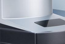
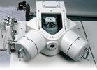
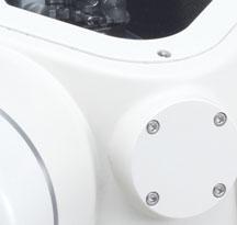
15 Scanning Probe Microscope SPM Unit Example of Optical Microscope Setups SPM Head Cantilever Holder Head-Slide Mechanism Scanner Z-Axis Coarse Adjustment Mechanism Stage High Magnification Optical Microscope Unit (with CCD) Magnification of Display Monitor: 48 to 900 zoom (14-inch display mode) including coaxial epi-illumination Optical Microscope Unit (with CCD) Magnification of Display Monitor: 100 (14-inch display mode) Optical Microscope Unit (without CCD) Magnification: 40 (20 ocular and 2 objective) Example of Observing a Sample and Cantilever Using the High Magnification Optical Microscope Unit The splitter slide mechanism enables obtaining a bright optical microscope image. Field-of-View: 270 μm 180 μm Cantilever: NCH Splitter-Slide Mechanism OFF ON Integrated Vibration Damper (Japanese Patent No ) Cantilever Specifications for SPM Unit Consumable Parts Resolution XY: 0.2 nm, Z: 0.01 nmm Cantilever for contact mode SiN Set of 34 chips Max. Scanning Range (X, Y, Z) Stage Standard scanner X and Y: 30 μm Z: 5 μm Wide range scanner X and Y: 125 μm Z: 7 μm Deep scanner X and Y: 55 μm Z: 13 μm Narrow range scanner X and Y: 2.5 μm Z: 0.3 μm Max. sample size: 24 mm dia. 8 mm Sample replacement method: Head-slide mechanism with integrated displacement detection system and cantilever Samples can be replaced without removing cantilever. Sample securing method: Secured with magnets Cantilever for dynamic mode Cantilever for magnetic force mode (MFM) Cantilever for current mode Cantilever for surface potential mode (KFM) * Many other types of cantilevers are also available. Contact your Shimadzu representative for details. Si Si Si Si Set of 20 chips Set of 20 chips Set of 20 chips Set of 20 chips 14


16 Standard Functions Contact Mode This mode creates an image of displacement in the sample height direction by scanning the sample surface with the repulsive force acting between the cantilever tip and sample kept constant. Force curves can be measured as well. Lateral Force Mode (LFM) By detecting the amount of twist in the cantilever during contact mode scanning, an image can be created from information corresponding to lateral forces (friction) acting between the sample and cantilever. Dynamic Mode This mode vibrates the cantilever near its resonant frequency. Since the amplitude changes as the cantilever approaches the sample, a sample height displacement image can be created by moving the probe to keep the amplitude constant. Force curves can be measured as well. Force Modulation Mode This mode vibrates the sample at constant amplitude and frequency during contact mode scanning. The cantilever response is detected by separating it into its amplitude and phase components. This allows creating an image of differences in sample surface properties. Phase Mode This mode detects the phase shift delay in the cantilever vibration during dynamic mode scanning. This allows creating an image of differences in sample surface properties. Optional Functions Current Mode This mode applies a voltage between a conductive cantilever and sample during contact mode scanning and creates an image from the distribution of current flows. I/V measurement is also possible. A Force Mapping (special order) A force curve can be measured for each point in observed image data to observe a distribution of sample mechanical properties or adhesive strength. Adhesion layer Surface Potential Mode (KFM) An image can be created from the electric potential of the sample surface by applying an alternating current electrical signal to a conductive cantilever and detecting the static electric force acting between the sample surface and cantilever. Magnetic Force Mode (MFM) This mode scans the sample with a magnetic tipped cantilever kept at a constant distance from the sample. An image can be created from magnetic information of the sample surface obtained by detecting the magnetic force from the magnetic leakage field N S N S V Sample Vector Scanning (special order) The scanning direction, force between the probe and sample, or the applied voltage can be programmed to allow scanning according to a program. Petri Dish Type Solution Cell The sample is attached to the bottom of a small petri dish, which is then filled with solution. By scanning with the cantilever immersed in solution, AFM observations can be performed in solutions. Electrochemical Solution Cell This cell is used for AFM observations of sample surface changes while an electrochemical reaction occurs in an electrolytic solution. The cell includes three standard electrodes (working, counter, and reference) and includes a petri dish type solution cell. (Does not include the separately-ordered electrochemical controller (potentiostat).) Scanning Probe Microscope 15


17 Environment Controlled Scanning Probe Microscope WET-SPM Series 16

 and CH-III (with TMP), were designed specifically for the series as a")

18 SPM Observations in a Controlled Environment By adding an environment controlled chamber, the scanning probe microscope can be upgraded to a WET-SPM series system. This is only possible for the, which was optimized for operating within a controlled chamber, by including features such as a Shimadzu proprietary head-slide mechanism, operation from the front panel, fully automatic approach, and open head design. This is especially ideal for samples vulnerable to air or moisture. Environment Controlled Chamber CH- /CH- Chamber View Port SPM Unit These environment controlled chambers, CH-II (without TMP) and CH-III (with TMP), were designed specifically for the series as a chamber system with a built-in vibration damper. Since this enables controlling both the sample and surrounding environment, the SPM can be used to directly observe samples processed in a controlled environment (Japanese Patent No , US Patent No ). A large view port and dual glove ports allow pretreating samples inside the chamber. Adding the option for in-situ SPM permits real-time investigation of surface changes due to changes in physical parameters such as temperature, humidity, pressure, luminescence, and concentration. The SPM unit can be easily loaded into and unloaded from the chamber from the rear, allowing it to be used for both ambient atmosphere and controlled environment observations. Gas Introduction Mechanism Glove Port Turbomolecular Pump (CH-III only) Vibration Damper Specifications Port Pumps Used for Vacuum System Gas Introduction Mechanism Current Input Terminals (7-pin) Vibration Damper Glove port Large view port Unit loading port Sample loading port Pumping port Spare port Rotary pump (160 L/min) Turbomolecular pump (50 L/sec) (CH-III only) Single-circuit automatic control 16 (including spares) Integrated air-spring vibration damper Photo of Front Photo of Back Scanning Probe Microscope 17


19 WET-SPM Series Options Temperature and Humidity Controller Controller is attached to an environment controlled chamber to control the temperature and humidity inside the chamber. FC Film Observation with Environmentally Controlled Temperature and Humidity Low Temperature High Temperature Variations in the surface shape of Nafion film due to changes in humidity were observed. In each case, microscopic features of about a few nm in height were observed, but the images show that increasing the humidity results in smoother features and more swelling. Polymer Film 30 C 10%RH 30 C 80%RH Humidified Gas Generator Low Temperature High Temperature Variations in the shape of polymer film were observed using a controlled temperature and humidity environment. Gas Spray Unit Real Time Observation of Nickel Surface Variations The gas spray unit is attached to a spare port to spray small amounts of gas on the sample. The nickel surface's reaction to gas was observed continuously in real time. When the clean surface after reduction (left) started being sprayed with carbon monoxide, the change in shape was observed as carbonyl complexes were formed (right). (Data provided by former National Institute of Materials and Chemical Research) 18


20 Sample Heating and Cooling Unit Observation of Cooled Plastic The sample can be loaded into the unit and heated or cooled. Temperature Controller Topographic image Viscosity image Room Temperature Two separate phases were observed in the viscosity image. Topographic image Viscosity image Cooled to -30 C After cooling, there were almost no visible differences in viscosity. Sample Heating Unit Observation of Heated Polymer Film The sample can be loaded into the unit and heated. The unit can even be operated in atmospheric conditions, depending on the sample. 30 C Temperature Controller Heated Holder Installed in Scanner 50 C The phase image (right) clearly shows the changes in sample surface physical properties as the sample is heated. Light Irradiation Unit This unit enables the use of a fiber optic light to irradiate sample surfaces. It does not include the light source or the optical fiber. It can be operated in atmospheric conditions. Observation of Ultraviolet Light Irradiating Pentacene Thin Film on SrTiO3 Irradiation Before Irradiation 40 Minutes After Irradiation The pentacene thin film was formed as a cluster of two or three 1.6 nm thick layers. When irradiated with 365 nm wavelength ultraviolet light, the cluster structure gradually started breaking apart. After 40 minutes, the thin film cluster was mostly gone. During this time, there is negligible drift and observation is possible using the same field of view. (Data provided by Dr. Yuji Matsumoto, Frontier Research Center, Tokyo Institute of Technology) Scanning Probe Microscope 19
21 Specifications 1. SPM Unit Observation Modes Resolution SPM Head Scanner Stage Z-Axis Coarse Adjustment Mechanism Signal Display Panel Vibration Isolation System Optical Microscope Observation Specialized enclosure Environment Control 2. Control Unit Scan Controller Feedback Controller Data Acquisition Controller Communications Interface X/Y-axis control Z-axis control Control system Input signal Protocol 3. Data Processing Unit Host Computer Monitor Communications Interface Standard Optional X, Y Z Displacement detection system Light source Detector Drive element Max. scanning size (X, Y, Z) Max. sample size Sample replacement method Sample securing method Method Max. stroke Displayed quantity Vibration Damper Method Method Method Operating system RAM Strorage Graphics Panel Protocol Contact Dynamic Phase Lateral Force (LFM) Force Modulation Magnetic Force (MFM) Current Surface Potential (KFM) 0.2 nm 0.01 nm Light source/optical lever/detector Laser diode (ON/OFF) Irradiates cantilever continuously, even while replacing samples. Photodetector Tube piezoelectric element 30 μm 30 μm 5 μm 125 μm 125 μm 7 μm (optional) 55 μm 55 μm 13 μm (optional) 2.5 μm 2.5 μm 0.3 μm (optional) 24 mm dia. 8 mm Head-slide mechanism with integrated displacement detection system and cantilever Samples can be replaced without removing cantilever. Magnet Automatic, using stepping motor Fully automatic, regardless of sample thickness 10 mm Total incident light to detector (digital display) Built into SPM unit Beam-splitter slide mechanism Not necessary or environment controlled chamber is used. Chamber can be added without modifying SPM unit. ±211 V, full time 16-bit accuracy ±211 V, max. 26-bit accuracy Digital control by DSP 5 channels (standard) 7 channels (optional) TCP/IP Windows 7 Professional (32-bit), English version 2GB min HDD 160GB min. CD-RW drive memory : 256MB min. Flat panel display Display resolution : pixels TCP/IP 4. Software Online Offline Input Signal Image data display Scanning direction Scanning size Number of pixels Data size Observation window Profile display Status display Preset Calibration Scanning Signal display Navigator Image history Guidance Browser Image data display Line data display Image data processing Image data analysis File output Select from up to 6 signals. Maximum 8 images can be displayed simultaneously. Trace/retrace (simultaneous observation possible) Angle setting can be changed. 0.1 nm to max. scanning size (depending on scanner type) Offset setting can be changed , , , , , 64 64, Approx. 16 MB to 64 KB/data Multiple frames display: 1 frame, frames, 2 frame, frames (Vertical or Horizontal), or 4 frame, frames Z-axis display range settings (display range, offset) Color palette settings (400 types) Tilt correction setting Image history display modes (list, single screen) Display cross-section profile during scanning, and save (both directions). Display cross-section profile at scanning position, analyze profile between any two points. Display the operating status of the main unit. Register and retrieve parameter settings. Independent calibration of each axis (X, Y, and Z) Switch XY-scanning ON/OFF Switch Y-scanning ON/OFF Y-scanning can be restarted. Y-scanning start position can be changed (top, center, or bottom). Display detector vertical/horizontal variation signal. Display feedback signal. Display laser intensity. Display scanning size, move positions, change scanning size, change angle. Load and display image data. Display list of saved images or display saved images. Display cross-section profile or analyze profile between any two points. Display operating procedures. List in thumbnail mode Delete, copy, move, or search data. Change group names or data names. Create/delete folders. Variable shade image (top view) display (length measurement possible) Pseudo-3D display, 3D display Zoom in/out or rotate 3D display (mouse operation possible) Analyze cross-section profile of 3D display. Set light source, view angle, and gloss settings for 3D-image display. Display contour lines. Create, edit, and select color palettes. Change Z-axis range setting, set Z-axis units. Reduce/enlarge image, create as icon. Display image data information (parameters, image processing history, comments). Enter and display comments. Overlay, tile, overwrite. Line colors can be changed. Reduce/enlarge image, create as icon. Flatten, erase noisy lines. Local filter, spectrum filter Zoom, invert, and rotate image. Resample, extract lines, use macro functions. Profile analysis, line roughness analysis. Surface roughness analysis, topography analysis, step measurement. Power spectrum analysis, autocorrelation analysis Fractal analysis, line length analysys, line roughness analysis DIB formant (bitmap) TIFF format, ASCII format * Windows is a registered trademark of Microsoft Corporation in the United States and/or other countries. * Other company names and product names mentioned in this document are trademarks or registered trademarks of their respective companies. * TM and symbols are omitted in this document. 20


22 Installation Specifications Installation Environment The following conditions are appropriate for the room where the SPM is installed. Temperature : 23 C ± 5 C Relative Humidity : 60 % max. Power Supply The following power supply is required to operate the. Single-phase V / V, 50/60 Hz, 15 A - 2 circuits Grounding Resistance: 100 max. * The power supply indicated above is for a basic configuration of the and can vary depending on the options included. Please see specifications for details. Environment Controlled Chamber Single-phase V, 50/60 Hz, 15 A - 2 circuits Grounding Resistance: 100 max. Size and Weight of Units SPM Unit Controller Environment Controlled Chamber W180 D255 H260mm 5.5kg W250 D420 H454mm 18.5kg W1170 D725 H1055mm 210kg Installation Example * Figure shows example of one possible configuration. Front View WET-SPM Front View Top View Top View 800mm 600mm 800mm 725mm 650mm 450mm 1200mm 800mm 1200mm 1170mm * Dimensions for the computer table and desk-type air-spring vibration damper are only indicated for reference purposes. * Dimensions for the computer table are only indicated for reference purposes. Scanning Probe Microscope 21
23 Company names, product/service names and logos used in this publication are trademarks and trade names of Shimadzu Corporation or its affiliates, whether or not they are used with trademark symbol TM or. Third-party trademarks and trade names may be used in this publication to refer to either the entities or their products/services. Shimadzu disclaims any proprietary interest in trademarks and trade names other than its own. For Research Use Only. Not for use in diagnostic procedures. The contents of this publication are provided to you as is without warranty of any kind, and are subject to change without notice. Shimadzu does not assume any responsibility or liability for any damage, whether direct or indirect, relating to the use of this publication. Shimadzu Corporation, 2012 Printed in Japan ANS
Measurement of Microscopic Three-dimensional Profiles with High Accuracy and Simple Operation
 238 Hitachi Review Vol. 65 (2016), No. 7 Featured Articles Measurement of Microscopic Three-dimensional Profiles with High Accuracy and Simple Operation AFM5500M Scanning Probe Microscope Satoshi Hasumura
SMX-1000 Plus SMX-1000L Plus
 Microfocus X-Ray Inspection Systems SMX-1000 Plus SMX-1000L Plus C251-E023A Taking Innovation to New Heights with Shimadzu X-Ray Inspection Systems Microfocus X-Ray Inspection Systems SMX-1000 Plus SMX-1000L
Atomic Force Microscopy (Bruker MultiMode Nanoscope IIIA)
") Atomic Force Microscopy (Bruker MultiMode Nanoscope IIIA) This operating procedure intends to provide guidance for general measurements with the AFM. For more advanced measurements or measurements with
Atomic Force Microscopy (Bruker MultiMode Nanoscope IIIA) This operating procedure intends to provide guidance for general measurements with the AFM. For more advanced measurements or measurements with
INDIAN INSTITUTE OF TECHNOLOGY BOMBAY
 IIT Bombay requests quotations for a high frequency conducting-atomic Force Microscope (c-afm) instrument to be set up as a Central Facility for a wide range of experimental requirements. The instrument
Magnetic Micro Testing System Microservo MMT Series C225-E014A
 Magnetic Micro Testing System Microservo MMT Series C225-E014A Microservo MMT Series Magnetic Micro Testing System In recent years strength evaluation of micro materials and micro parts is increasing its
Optical Microscope. Active anti-vibration table. Mechanical Head. Computer and Software. Acoustic/Electrical Shield Enclosure
 Optical Microscope On-axis optical view with max. X magnification Motorized zoom and focus Max Field of view: mm x mm (depends on zoom) Resolution : um Working Distance : mm Magnification : max. X Zoom
Akiyama-Probe (A-Probe) guide
 guide") Akiyama-Probe (A-Probe) guide This guide presents: what is Akiyama-Probe, how it works, and what you can do Dynamic mode AFM Version: 2.0 Introduction NANOSENSORS Akiyama-Probe (A-Probe) is a self-sensing
Akiyama-Probe (A-Probe) guide This guide presents: what is Akiyama-Probe, how it works, and what you can do Dynamic mode AFM Version: 2.0 Introduction NANOSENSORS Akiyama-Probe (A-Probe) is a self-sensing
Nanosurf easyscan 2 FlexAFM
 Nanosurf easyscan 2 FlexAFM Your Versatile AFM System for Materials and Life Science www.nanosurf.com The new Nanosurf easyscan 2 FlexAFM scan head makes measurements in liquid as simple as measuring in
Akiyama-Probe (A-Probe) guide
 guide") Akiyama-Probe (A-Probe) guide This guide presents: what is Akiyama-Probe, how it works, and its performance. Akiyama-Probe is a patented technology. Version: 2009-03-23 Introduction NANOSENSORS Akiyama-Probe
Akiyama-Probe (A-Probe) guide This guide presents: what is Akiyama-Probe, how it works, and its performance. Akiyama-Probe is a patented technology. Version: 2009-03-23 Introduction NANOSENSORS Akiyama-Probe
Standard Operating Procedure of Atomic Force Microscope (Anasys afm+)
") Standard Operating Procedure of Atomic Force Microscope (Anasys afm+) The Anasys Instruments afm+ system incorporates an Atomic Force Microscope which can scan the sample in the contact mode and generate
Standard Operating Procedure of Atomic Force Microscope (Anasys afm+) The Anasys Instruments afm+ system incorporates an Atomic Force Microscope which can scan the sample in the contact mode and generate
nanovea.com PROFILOMETERS 3D Non Contact Metrology
 PROFILOMETERS 3D Non Contact Metrology nanovea.com PROFILOMETER INTRO Nanovea 3D Non-Contact Profilometers are designed with leading edge optical pens using superior white light axial chromatism. Nano
Outline: Introduction: What is SPM, history STM AFM Image treatment Advanced SPM techniques Applications in semiconductor research and industry
 1 Outline: Introduction: What is SPM, history STM AFM Image treatment Advanced SPM techniques Applications in semiconductor research and industry 2 Back to our solutions: The main problem: How to get nm
Infrared Microscope AIM-9000 C103-E103B
 Infrared Microscope C103-E103B Wide-Field Camera Automatic Recognition Automatic Qualitative High Sensitivity Finally, a wide view on micro sample analysis Surface Micro SHIMADZU AIMs to provide analysis
inspexio SMX-225CT FPD HR
 Microfocus X-Ray CT System C251-E029A Advanced Operability and Excellent Image Quality That Overturns Conventional Assumptions Microfocus X-Ray CT System The is a high-performance microfocus X-ray CT system
Standard Operating Procedure
 Standard Operating Procedure Nanosurf Atomic Force Microscopy Operation Facility NCCRD Nanotechnology Center for Collaborative Research and Development Department of Chemistry and Engineering Physics The
Imaging Carbon Nanotubes Magdalena Preciado López, David Zahora, Monica Plisch
 Imaging Carbon Nanotubes Magdalena Preciado López, David Zahora, Monica Plisch I. Introduction In this lab you will image your carbon nanotube sample from last week with an atomic force microscope. You
INTRODUCTION We believe that every laboratory working in the field of nanotechnology needs an SEM, therefore we would like to introduce to you our IEM
 INTRODUCTION We believe that every laboratory working in the field of nanotechnology needs an SEM, therefore we would like to introduce to you our IEM series of SEM. In short space of time, our device
NanoFocus Inc. Next Generation Scanning Probe Technology. Tel : Fax:
 NanoFocus Inc. Next Generation Scanning Probe Technology www.nanofocus.kr Tel : 82-2-864-3955 Fax: 82-2-864-3956 Albatross SPM is Multi functional research grade system Flexure scanner and closed-loop
Nanonics Systems are the Only SPMs that Allow for On-line Integration with Standard MicroRaman Geometries
 Nanonics Systems are the Only SPMs that Allow for On-line Integration with Standard MicroRaman Geometries 2002 Photonics Circle of Excellence Award PLC Ltd, England, a premier provider of Raman microspectral
UNIVERSITY OF WATERLOO Physics 360/460 Experiment #2 ATOMIC FORCE MICROSCOPY
 UNIVERSITY OF WATERLOO Physics 360/460 Experiment #2 ATOMIC FORCE MICROSCOPY References: http://virlab.virginia.edu/vl/home.htm (University of Virginia virtual lab. Click on the AFM link) An atomic force
Quick and simple installation and no maintenance needed. 3 Times More affordable Than a normal SEM. Obtaining results in less than 4 minutes
 INTRODUCTION We believe that every laboratory working in the field of nanotechnology needs an SEM, therefore we would like to introduce to you our IEM series of SEM. In short space of time, our device
 07 Setting Place a specimen, and select a fluorescence dye. The FV10i automatically selects the most suitable imaging conditions based on the fluorescence dye selection. Set Image mapping menu Just click
Measurement of Surface Profile and Layer Cross-section with Wide Field of View and High Precision
 Hitachi Review Vol. 65 (2016), No. 7 243 Featured Articles Measurement of Surface Profile and Layer Cross-section with Wide Field of View and High Precision VS1000 Series Coherence Scanning Interferometer
Systematic Workflow via Intuitive GUI. Easy operation accomplishes your goals faster than ever.
 Systematic Workflow via Intuitive GUI Easy operation accomplishes your goals faster than ever. 16 With the LEXT OLS4100, observation or measurement begins immediately once the sample is placed on the stage.
Prepare Sample 3.1. Place Sample in Stage. Replace Probe (optional) Align Laser 3.2. Probe Approach 3.3. Optimize Feedback 3.4. Scan Sample 3.
 Align Laser 3.2. Probe Approach 3.3. Optimize Feedback 3.4. Scan Sample 3.") CHAPTER 3 Measuring AFM Images Learning to operate an AFM well enough to get an image usually takes a few hours of instruction and practice. It takes 5 to 10 minutes to measure an image if the sample is
CHAPTER 3 Measuring AFM Images Learning to operate an AFM well enough to get an image usually takes a few hours of instruction and practice. It takes 5 to 10 minutes to measure an image if the sample is
Nanovie. Scanning Tunnelling Microscope
 Nanovie Scanning Tunnelling Microscope Nanovie STM Always at Hand Nanovie STM Lepto for Research Nanovie STM Educa for Education Nanovie Auto Tip Maker Nanovie STM Lepto Portable 3D nanoscale microscope
Scanning Ion Conductance Microscope ICnano
 Sperm Cell Epithelial Cells I nner Ear Hair Cells I nner Ear Hair Cell Neurons E- Coli Bac teria Scanning Ion Conductance Microscope ICnano About ionscope About ionscope The ionscope scanning ion conductance
Radial Polarization Converter With LC Driver USER MANUAL
 ARCoptix Radial Polarization Converter With LC Driver USER MANUAL Arcoptix S.A Ch. Trois-portes 18 2000 Neuchâtel Switzerland Mail: info@arcoptix.com Tel: ++41 32 731 04 66 Principle of the radial polarization
- Near Field Scanning Optical Microscopy - Electrostatic Force Microscopy - Magnetic Force Microscopy
 - Near Field Scanning Optical Microscopy - Electrostatic Force Microscopy - Magnetic Force Microscopy Yongho Seo Near-field Photonics Group Leader Wonho Jhe Director School of Physics and Center for Near-field
Microscopic Structures
 Microscopic Structures Image Analysis Metal, 3D Image (Red-Green) The microscopic methods range from dark field / bright field microscopy through polarisation- and inverse microscopy to techniques like
Zeta-20. Zeta3D OPTICAL PROFILER IMAGING THE IMPOSSIBLE
 Zeta3D OPTICAL PROFILER Zeta-20 IMAGING THE IMPOSSIBLE TRUE COLOR 3D DIC BRIGHT FIELD DARK FIELD POLARIZED LIGHT IMAGE THROUGH TRANSMISSIVE IMAGE WHITE OR BLUE LED LIGHT SOURCE THIN FILM THICKNESS DIAMOND
Lecture 20: Optical Tools for MEMS Imaging
 MECH 466 Microelectromechanical Systems University of Victoria Dept. of Mechanical Engineering Lecture 20: Optical Tools for MEMS Imaging 1 Overview Optical Microscopes Video Microscopes Scanning Electron
Introduction of New Products
 Field Emission Electron Microscope JEM-3100F For evaluation of materials in the fields of nanoscience and nanomaterials science, TEM is required to provide resolution and analytical capabilities that can
Investigate in magnetic micro and nano structures by Magnetic Force Microscopy (MFM)
") Investigate in magnetic micro and nano 5.3.85- Related Topics Magnetic Forces, Magnetic Force Microscopy (MFM), phase contrast imaging, vibration amplitude, resonance shift, force Principle Caution! -
Investigate in magnetic micro and nano 5.3.85- Related Topics Magnetic Forces, Magnetic Force Microscopy (MFM), phase contrast imaging, vibration amplitude, resonance shift, force Principle Caution! -
Cutting-edge Atomic Force Microscopy techniques for large and multiple samples
 Cutting-edge Atomic Force Microscopy techniques for large and multiple samples Study of up to 200 mm samples using the widest set of AFM modes Industrial standards of automation A unique combination of
Basic methods in imaging of micro and nano structures with atomic force microscopy (AFM)
") Basic methods in imaging of micro and nano P2538000 AFM Theory The basic principle of AFM is very simple. The AFM detects the force interaction between a sample and a very tiny tip (
Basic methods in imaging of micro and nano P2538000 AFM Theory The basic principle of AFM is very simple. The AFM detects the force interaction between a sample and a very tiny tip (
Technical Explanation for Displacement Sensors and Measurement Sensors
 Technical Explanation for Sensors and Measurement Sensors CSM_e_LineWidth_TG_E_2_1 Introduction What Is a Sensor? A Sensor is a device that measures the distance between the sensor and an object by detecting
A Laser-Based Thin-Film Growth Monitor
 TECHNOLOGY by Charles Taylor, Darryl Barlett, Eric Chason, and Jerry Floro A Laser-Based Thin-Film Growth Monitor The Multi-beam Optical Sensor (MOS) was developed jointly by k-space Associates (Ann Arbor,
A Project Report Submitted to the Faculty of the Graduate School of the University of Minnesota By
 Observation and Manipulation of Gold Clusters with Scanning Tunneling Microscopy A Project Report Submitted to the Faculty of the Graduate School of the University of Minnesota By Dogukan Deniz In Partial
Indian Institute of Technology Bombay
 Specifications for High Resolution Scanning Probe Microscope Item Essential measuring modes with complete hardware and software. All the modes should be demonstrated during installation & training Scanners
Zeta-300 3D OPTICAL PROFILER
 Zeta-300 3D OPTICAL PROFILER Technology Toolkit Developed in 2007, the revolutionary Confocal Grid Structured Illumination (CGSI) is the powerful technology in all Zeta Optical Profilers but in a Zeta,
University of MN, Minnesota Nano Center Standard Operating Procedure
 Equipment Name: Atomic Force Microscope Badger name: afm DI5000 PAN Revisionist Paul Kimani Model: Dimension 5000 Date: October 6, 2017 Location: Bay 1 PAN Revision: 1 A. Description i. Enhanced Motorized
Horiba LabRAM ARAMIS Raman Spectrometer Revision /28/2016 Page 1 of 11. Horiba Jobin-Yvon LabRAM Aramis - Raman Spectrometer
 Page 1 of 11 Horiba Jobin-Yvon LabRAM Aramis - Raman Spectrometer The Aramis Raman system is a software selectable multi-wavelength Raman system with mapping capabilities with a 400mm monochromator and
Advanced Nanoscale Metrology with AFM
 Advanced Nanoscale Metrology with AFM Sang-il Park Corp. SPM: the Key to the Nano World Initiated by the invention of STM in 1982. By G. Binnig, H. Rohrer, Ch. Gerber at IBM Zürich. Expanded by the invention
AFM of High-Profile Surfaces
 AFM of High-Profile Surfaces Fig. 1. AFM topograpgy image of black Si made using SCD probe tip. Scan size 4. Profile height is more than 8. See details and other application examples below. High Aspect
Manufacturing Metrology Team
 The Team has a range of state-of-the-art equipment for the measurement of surface texture and form. We are happy to discuss potential measurement issues and collaborative research Manufacturing Metrology
Microscopy from Carl Zeiss
 Microscopy from Carl Zeiss Contents Page Contents... 1 Introduction... 1 Starting the System... 2 Introduction to ZEN Efficient Navigation... 5 Setting up the microscope... 10 Configuring the beam path
Basic Users Manual for Tecnai-F20 TEM
 Basic Users Manual for Tecnai-F20 TEM NB: This document contains my personal notes on the operating procedure of the Tecnai F20 and may be used as a rough guide for those new to the microscope. It may
Installation & User Manual Micro-Image Capture 7
 Installation & User Manual Micro-Image Capture 7 Ver1.2016 Product Warranty Quality Assurance Every Micro-Image Capture system passes quality assurance tests including focus, resolution quality and mechanical
MEMS for RF, Micro Optics and Scanning Probe Nanotechnology Applications
 MEMS for RF, Micro Optics and Scanning Probe Nanotechnology Applications Part I: RF Applications Introductions and Motivations What are RF MEMS? Example Devices RFIC RFIC consists of Active components
Nanoscale Material Characterization with Differential Interferometric Atomic Force Microscopy
 Nanoscale Material Characterization with Differential Interferometric Atomic Force Microscopy F. Sarioglu, M. Liu, K. Vijayraghavan, A. Gellineau, O. Solgaard E. L. Ginzton Laboratory University Tip-sample
LITE /LAB /SCAN /INLINE:
 Metis Metis LITE /LAB /SCAN/ INLINE Metis LITE /LAB /SCAN /INLINE: Spectral Offline and Inline Measuring System, using Integrating Sphere, for coatings on foils/web and on large size glasses To ensure
Practical work no. 3: Confocal Live Cell Microscopy
 Practical work no. 3: Confocal Live Cell Microscopy Course Instructor: Mikko Liljeström (MIU) 1 Background Confocal microscopy: The main idea behind confocality is that it suppresses the signal outside
Bruker Dimension Icon AFM Quick User s Guide
 Bruker Dimension Icon AFM Quick User s Guide March 3, 2015 GLA Contacts Jingjing Jiang (jjiang2@caltech.edu 626-616-6357) Xinghao Zhou (xzzhou@caltech.edu 626-375-0855) Bruker Tech Support (AFMSupport@bruker-nano.com
Etch, Deposition, and Metrology Options for Cost-Effective Thin-Film Bulk Acoustic Resonator (FBAR) Production
 Production") Etch, Deposition, and Metrology Options for Cost-Effective Thin-Film Bulk Acoustic Resonator (FBAR) Production Figure 1 Veeco is driving System on a Chip Technology Frank M. Cumbo, Kurt E. Williams, John
Etch, Deposition, and Metrology Options for Cost-Effective Thin-Film Bulk Acoustic Resonator (FBAR) Production Figure 1 Veeco is driving System on a Chip Technology Frank M. Cumbo, Kurt E. Williams, John
Development of JEM-2800 High Throughput Electron Microscope
 Development of JEM-2800 High Throughput Electron Microscope Mitsuhide Matsushita, Shuji Kawai, Takeshi Iwama, Katsuhiro Tanaka, Toshiko Kuba and Noriaki Endo EM Business Unit, JEOL Ltd. Electron Optics
SPM The Industry s Performance Leader High Resolution Closed-loop System Fast, Easy Tip & Sample Exchange Versatility and Value Powerful Research
 SPM The Industry s Performance Leader High Resolution Closed-loop System Fast, Easy Tip & Sample Exchange Versatility and Value Powerful Research Flexibility Atomic resolution STM image of highly-oriented
Turnkey Solution for Technical Cleanliness Inspection
 Technical Cleanliness Inspection System CIX90 OLYMPUS CIX series Turnkey Solution for Technical Cleanliness Inspection Simplify Your Technical Cleanliness Standard process for cleanliness inspection: preparation
Introduction ORANGE PEEL / DOI. Structure size. Color Physical Properties Technical Service Index
 Introduction The total appearance and the visibility of structures depend on the structure size, the observing distance and the image forming quality. Structure size Surfaces with different structure sizes
Experiment 1: Fraunhofer Diffraction of Light by a Single Slit
 Experiment 1: Fraunhofer Diffraction of Light by a Single Slit Purpose 1. To understand the theory of Fraunhofer diffraction of light at a single slit and at a circular aperture; 2. To learn how to measure
CD-SEM for 65-nm Process Node
 CD-SEM for 65-nm Process Node 140 CD-SEM for 65-nm Process Node Hiroki Kawada Hidetoshi Morokuma Sho Takami Mari Nozoe OVERVIEW: Inspection equipment for 90-nm and subsequent process nodes is required
FRAUNHOFER AND FRESNEL DIFFRACTION IN ONE DIMENSION
 FRAUNHOFER AND FRESNEL DIFFRACTION IN ONE DIMENSION Revised November 15, 2017 INTRODUCTION The simplest and most commonly described examples of diffraction and interference from two-dimensional apertures
; A=4π(2m) 1/2 /h. exp (Fowler Nordheim Eq.) 2 const
 1/2 /h. exp (Fowler Nordheim Eq.) 2 const") Scanning Tunneling Microscopy (STM) Brief background: In 1981, G. Binnig, H. Rohrer, Ch. Gerber and J. Weibel observed vacuum tunneling of electrons between a sharp tip and a platinum surface. The tunnel
Scanning Tunneling Microscopy (STM) Brief background: In 1981, G. Binnig, H. Rohrer, Ch. Gerber and J. Weibel observed vacuum tunneling of electrons between a sharp tip and a platinum surface. The tunnel
Instructions for easyscan Atomic Force Microscope
 UVA's Hands-on Introduction to Nanoscience Instructions for easyscan Atomic Force Microscope (revision 8 November 2012) NOTE: Instructions assume software is pre-configured per "UVA Instructor Guide for
attosnom I: Topography and Force Images NANOSCOPY APPLICATION NOTE M06 RELATED PRODUCTS G
 APPLICATION NOTE M06 attosnom I: Topography and Force Images Scanning near-field optical microscopy is the outstanding technique to simultaneously measure the topography and the optical contrast of a sample.
PAINT BORER 518 MC PAINTXPLORER 548
 PAINT BORER 518 USB PAINT BORER 518 MC PAINTXPLORER 548 PAINT BORER 518 USB Thickness measurements in accordance with the standardised wedge cut method PAINT BORER 518 MC PAINTXPLORER 548 testing equipment
Quality Performance, Innovative Design
 Dimensions Confocal Laser Scanning Biological Microscope Table size (mm): 1400(W) 800(D) * Table is not available from Olympus. Avoid placing the controller directly on the floor. Dimensions / Weight /
Super High Vertical Resolution Non-Contact 3D Surface Profiler BW-S500/BW-D500 Series
 Super High Vertical Resolution Non-Contact 3D Surface Profiler BW-S500/BW-D500 Series Nikon's proprietary scanning-type optical interference measurement technology achieves 1pm* height resolution. * Height
Optical Measurement P-1
 Optical Measurement P-1 FAST ROUND PART INSPECTION The whole TESA-Scan product line belongs to the range of dedicated non-contact opto-electronic measuring centres that provide Users with a complete solution
JEM-F200. Multi-purpose Electron Microscope. Scientific / Metrology Instruments Multi-purpose Electron Microscope
 Scientific / Metrology Instruments Multi-purpose Electron Microscope JEM-F200 Multi-purpose Electron Microscope JEM-F200/F2 is a multi-purpose electron microscope of the new generation to meet today's
WITec Alpha 300R Quick Operation Summary October 2018
 WITec Alpha 300R Quick Operation Summary October 2018 This document is frequently updated if you feel information should be added, please indicate that to the facility manager (currently Philip Carubia,
Morphologi. Advanced image analysis for high sensitivity particle characterization. Particle size. Particle shape
 Particle size Particle shape Morphologi detailed specification sheets from www.malvern.co.uk Introducing a new concept in image analysis The Morphologi high sensitivity particle analyzer is more than just
Hybrid Surface Contour Measuring Machine FORMTRACER CS-5000
 Form Measurement Hybrid Surface Contour Measuring Machine FORMTRCER CS-5000 CTLOG No. E4220-525 hybrid surface contour measuring machine that combines contour and surface roughness measurements and analyses
PicoMaster 100. Unprecedented finesse in creating 3D micro structures. UV direct laser writer for maskless lithography
 UV direct laser writer for maskless lithography Unprecedented finesse in creating 3D micro structures Highest resolution in the market utilizing a 405 nm diode laser Structures as small as 300 nm 375 nm
Infrared Microscope. Dedicated AIMsolution Software. Hisato Fukuda. 1. Introduction. 2. Automatic Contaminant Recognition Function
 C103-E120 Vol. 28 Infrared Microscope Dedicated AIMsolution Software ------- 02 Infrared Microscope Using Imaging Analysis ------- 05 EDXIR-Analysis EDX-FTIR Contaminant Finder/Material Inspector -------
Applications of Piezoelectric Actuator
 MAMIYA Yoichi Abstract The piezoelectric actuator is a device that features high displacement accuracy, high response speed and high force generation. It has mainly been applied in support of industrial
SCIENTIFIC INSTRUMENT NEWS. Introduction. Design of the FlexSEM 1000
 SCIENTIFIC INSTRUMENT NEWS 2017 Vol. 9 SEPTEMBER Technical magazine of Electron Microscope and Analytical Instruments. Technical Explanation The FlexSEM 1000: A Scanning Electron Microscope Specializing
YOUNGS MODULUS BY UNIFORM & NON UNIFORM BENDING OF A BEAM
 YOUNGS MODULUS BY UNIFORM & NON UNIFORM BENDING OF A BEAM RECTANGULAR BEAM PLACED OVER TWO KNIFE EDGES & DISTANCE BETWEEN KNIFE EDGES IS KEPT CONSTANT AS l= 50cm UNIFORM WEIGHT HANGERS ARE SUSPENDED WITH
Micro-manipulated Cryogenic & Vacuum Probe Systems
 Janis micro-manipulated probe stations are designed for non-destructive electrical testing using DC, RF, and fiber-optic probes. They are useful in a variety of fields including semiconductors, MEMS, superconductivity,
OPTICS IN MOTION. Introduction: Competing Technologies: 1 of 6 3/18/2012 6:27 PM.
 1 of 6 3/18/2012 6:27 PM OPTICS IN MOTION STANDARD AND CUSTOM FAST STEERING MIRRORS Home Products Contact Tutorial Navigate Our Site 1) Laser Beam Stabilization to design and build a custom 3.5 x 5 inch,
Zeiss 880 Training Notes Zen 2.3
 Zeiss 880 Training Notes Zen 2.3 1 Turn on the HXP 120V Lamp 2 Turn on Main Power Switch Turn on the Systems PC Switch Turn on the Components Switch. 3 4 5 Turn on the PC and log into your account. Start
Applications of Steady-state Multichannel Spectroscopy in the Visible and NIR Spectral Region
 Feature Article JY Division I nformation Optical Spectroscopy Applications of Steady-state Multichannel Spectroscopy in the Visible and NIR Spectral Region Raymond Pini, Salvatore Atzeni Abstract Multichannel
Park NX-Hivac The world s most accurate and easy to use high vacuum AFM for failure analysis.
 Park NX-Hivac The world s most accurate and easy to use high vacuum AFM for failure analysis www.parkafm.com Park NX-Hivac High vacuum scanning for failure analysis applications 4 x 07 / Cm3 Current (µa)
Quick Guide. LSM 5 MP, LSM 510 and LSM 510 META. Laser Scanning Microscopes. We make it visible. M i c r o s c o p y f r o m C a r l Z e i s s
 LSM 5 MP, LSM 510 and LSM 510 META M i c r o s c o p y f r o m C a r l Z e i s s Quick Guide Laser Scanning Microscopes LSM Software ZEN 2007 August 2007 We make it visible. Contents Page Contents... 1
Akiyama-Probe (A-Probe) technical guide This technical guide presents: how to make a proper setup for operation of Akiyama-Probe.
 technical guide This technical guide presents: how to make a proper setup for operation of Akiyama-Probe.") Akiyama-Probe (A-Probe) technical guide This technical guide presents: how to make a proper setup for operation of Akiyama-Probe. Version: 2.0 Introduction To benefit from the advantages of Akiyama-Probe,
Akiyama-Probe (A-Probe) technical guide This technical guide presents: how to make a proper setup for operation of Akiyama-Probe. Version: 2.0 Introduction To benefit from the advantages of Akiyama-Probe,
Thermo Scientific SPECTRONIC 200 Visible Spectrophotometer. The perfect. teaching instrument
 Thermo Scientific SPECTRONIC 200 Visible Spectrophotometer The perfect teaching instrument Designed for the Teaching Laboratory Thermo Scientific SPECTRONIC spectrophotometers have served as core analytical
Fast Laser Raman Microscope RAMAN
 Fast Laser Raman Microscope RAMAN - 11 www.nanophoton.jp Fast Raman Imaging A New Generation of Raman Microscope RAMAN-11 developed by Nanophoton was created by combining confocal laser microscope technology
LECTURE 10. Dr. Teresa D. Golden University of North Texas Department of Chemistry
 LECTURE 10 Dr. Teresa D. Golden University of North Texas Department of Chemistry Components for the source include: -Line voltage supply -high-voltage generator -x-ray tube X-ray source requires -high
Thermo Scientific SPECTRONIC 200 Education
 molecular spectroscopy Thermo Scientific SPECTRONIC 200 Education Part of Thermo Fisher Scientific Designed for the Teaching Laboratory Classroom Friendly Sample Compartment Whether you measure in 10 mm
attocfm I for Surface Quality Inspection NANOSCOPY APPLICATION NOTE M01 RELATED PRODUCTS G
 APPLICATION NOTE M01 attocfm I for Surface Quality Inspection Confocal microscopes work by scanning a tiny light spot on a sample and by measuring the scattered light in the illuminated volume. First,
ScanArray Overview. Principle of Operation. Instrument Components
 ScanArray Overview The GSI Lumonics ScanArrayÒ Microarray Analysis System is a scanning laser confocal fluorescence microscope that is used to determine the fluorescence intensity of a two-dimensional
Nexera Method Scouting
 Ultra High Performance Liquid Chromatograph Method Scouting System Nexera Method Scouting C190-E150A Maximizing Efficiency for Method Development The Nexera Method Scouting System design is based on the
LSM 780 Confocal Microscope Standard Operation Protocol
 LSM 780 Confocal Microscope Standard Operation Protocol Basic Operation Turning on the system 1. Sign on log sheet according to Actual start time 2. Check Compressed Air supply for the air table 3. Switch
Spatial intensity distribution analysis Matlab user guide
 Spatial intensity distribution analysis Matlab user guide August 2011 Guide on how to use the SpIDA graphical user interface. This little tutorial provides a step by step tutorial explaining how to get
Chapter Ray and Wave Optics
 109 Chapter Ray and Wave Optics 1. An astronomical telescope has a large aperture to [2002] reduce spherical aberration have high resolution increase span of observation have low dispersion. 2. If two
S.No Description/Specifications Qty 01. Post office box Trainer.
 Specification of Equipments for Physics lab S.No Description/Specifications Qty 01. Post office box Trainer. 06 The trainer should have: On Board DC Power Supply : 5V Galvanometer ; Deflection : 30 0 30
Optical Monitoring System Enables Greater Accuracy in Thin-Film Coatings. Line Scan Cameras What Do They Do?
 November 2017 Optical Monitoring System Enables Greater Accuracy in Thin-Film Coatings Line Scan Cameras What Do They Do? Improved Surface Characterization with AFM Imaging Supplement to Tech Briefs CONTENTS
INTERFEROMETER VI-direct
 Universal Interferometers for Quality Control Ideal for Production and Quality Control INTERFEROMETER VI-direct Typical Applications Interferometers are an indispensable measurement tool for optical production
Spotlight 150 and 200 FT-IR Microscopy Systems
 S P E C I F I C A T I O N S Spotlight 150 and 200 FT-IR Microscopy Systems FT-IR Microscopy Spotlight 200 with Frontier FT-IR Spectrometer Introduction PerkinElmer Spotlight FT-IR Microscopy Systems are