CHARACTERISTICS AND APPLICATIONS OF A SCANNING NANO-SLIT OPTICAL SENSOR. Anoop George. A Dissertation Submitted to the Faculty of the
|
|
|
- Aron Welch
- 6 years ago
- Views:
Transcription
1 1 CHARACTERISTICS AND APPLICATIONS OF A SCANNING NANO-SLIT OPTICAL SENSOR By Anoop George A Dissertation Submitted to the Faculty of the COLLEGE OF OPTICAL SCIENCES In Partial Fulfillment of the Requirements For the Degree of DOCTOR OF PHILOSOPHY In the Graduate College THE UNIVERSITY OF ARIZONA 2011
2 2 THE UNIVERSITY OF ARIZONA GRADUATE COLLEGE As members of the Dissertation Committee, we certify that we have read the dissertation prepared by Anoop George entitled Characteristics and Applications of a Scanning Nano-Slit Optical Sensor and recommend that it be accepted as fulfilling the dissertation requirement for the Degree of Doctor of Philosophy. Date: 02/09/11 Thomas D. Milster Date: 02/09/11 James H. Burge Date: 02/09/11 Matthew A. Kupinski Final approval and acceptance of this dissertation is contingent upon the candidate s submission of the final copies of the dissertation to the Graduate College I hereby certify that I have read this dissertation prepared under my direction and recommend that it be accepted as fulfilling the dissertation requirement. Date: 02/09/11 Dissertation Director: Thomas D. Milster
3 3 STATEMENT BY AUTHOR This dissertation has been submitted in partial fulfillment of requirements for an advanced degree at the University of Arizona and is deposited in the University Library to be made available to borrowers under rules of the library. Brief quotations from this dissertation are allowable without special permission, provided that accurate acknowledgement of source is made. Requests for permission for extended quotation from or reproduction of this manuscript in whole or in part may be granted by the head of the major department or the Dean of the Graduate College when in his or her judgment the proposed use of the material is in the interests of scholarship. In all other instances, however, permission must be obtained from the author. SIGNED: Anoop George
4 4 ACKNOWLEDGEMENTS I would first and foremost like to thank my advisor Dr. Tom D. Milster for his constant support, encouragement and guidance throughout my graduate studies. His passion for science and learning as well as his close mentoring of my scientific efforts will continue to have lasting effects on my post-graduate career. Moreover, I am extremely thankful for his friendship and I deeply cherish it. I would like to express my gratitude to my dissertation committee, Dr. James Burge and Dr. Matthew Kupinski for their insight and contributions to this work during the research and writing process. I also greatly appreciate the help and guidance provided by Dr. Yasuyuki Unno of Canon USA, Inc. A special thanks to Warren Bletscher and Delbert Hansen who came to my rescue many times and helped me with electronics and opto-mechanical aspects of my research. Furthermore, I would like to thank Jun Zhang, Dr. Young-Sik Kim, Seung-Hune Yang, Tao Chen, Tae-Young Choi, Matt Lang, Eric Aspnes, Dongyel Kang, Thiago Jota, Dr. Pramod Khulbe, Melissa Zaverton, Justin Sierchio, Phat Lu, Victor Densmore and Manal Khreishi for their help and support during my time as a graduate student. Many thanks to Gail Varin, Pat Gransie, Juliet Hughes, Tammy Orr and Dr. Carl Maes for their support during my time here. I would also like to thank all my friends in Tucson and at the College of Optical Sciences for making my experience a wonderful one. I would like to express my deep appreciation for my parents who encouraged me through every step of my student life. A million thanks to Lily for her support and love and for standing beside me through it all. I owe my success and dedicate this dissertation to them.
5 5 DEDICATIONS To my parents for their love and inspiration To my wife Lily for her patience and support
6 6 TABLE OF CONTENTS LIST OF ILLUSTRATIONS...8 ABSTRACT...12 CHAPTER 1 INTRODUCTION Basic Description of Research Motivation for This Study Outline of Dissertation...17 CHAPTER 2 BACKGROUND Near-Field Scanning Optical Microscope (NSOM / SNOM) Tomographic Imaging Transmission Properties of a Nano-Slit Current Scanning-Slit Applications Laser Beam Evaluation Aerial Image Evaluation in Lithography...36 CHAPTER 3 PRESENT STUDY Characterization of Coherent Nano-Slit Imaging Design and Fabrication Simulation Techniques for Nano-Slit Studies Experimental Apparatus of Scanning Slit Sensor Image Analysis Applications Measurement of a Sub-Micron Spot Distribution High NA, Partially Coherent Imaging MTF Measurements Image Reconstruction...61 CHAPTER 4 CONCLUSIONS Summary of Dissertation Future Work...67 REFERENCES...69 APPENDIX A REPRINT: CHARACTERISTICS OF A SCANNING NANO-SLIT IMAGE SENSOR FOR LINE-AND-SPACE PATTERNS...78 APPENDIX B MANUSCRIPT: SPOT DISTRIBUTION MEASUREMENT USING A SCANNING NANO-SLIT...89
7 7 TABLE OF CONTENTS Continued APPENDIX C MANUSCRIPT: HIGH NA, PARTIALLY COHERENT IMAGING WITH A TOMOGRAPHIC SCANNING NANO-SLIT APPENDIX D ANGULAR SPECTRUM PROPAGATION CODE APPENDIX E NANO-SLIT TOMOGRAPHIC IMAGING SLIMUATION CODE...157
8 8 LIST OF ILLUSTRATIONS Figure 2.1. (a) The SNOM probe structure. The defining regions include the tip, the taper and the transmitting fiber. Resolution is controlled by the morphology of the tip. (b) A 50 nm 50 nm SNOM aperture fabricated using FIB...21 Figure 2.2. Scanning probe optical microscopy geometries: (a) illumination mode (b) collection-mode (c) collection-mode oblique upon reflection and (d) probe illumination and collection upon reflection...22 Figure 2.3. Scanning near-field optical images ( = 1064 nm) of gold/palladium lines on a silicon wafer orientated (a) nearly perpendicular to and (b) nearly parallel to the slit aperture, with the corresponding signal profiles plotted in the diagrams below...24 Figure 2.4. Show here are four projections and the summation image which is formed by summing the four original back-projections. The original object was two absorbing disks of different sizes...26 Figure 2.5. (a) The classic Shepp-Logan phantom image (b) the projections of the image shown in (a) arranged to form a sinogram (c) The reconstructed image obtained by performing the filtered back-projection technique on the sinogram shown in (b)...27 Figure 2.6. (a) Schematic diagram of the scanned-and-rotated slit; the 150 m wide slit is perpendicular to the motion produced by stepper motor 1. This is used for obtaining a tomographic projection of the intensity distribution by rotating the disk plate with motor 2. (b) A 5.7 mm 4.7 mm reconstructed image, by means of the back-projection method, from the projection measurements obtained with the system shown in (a)...29 Figure 2.7. The following are results from a FDTD calculation with a wavelength of 1 m. The transmitted optical energy through a slit aperture on silver film, when the electric field is oriented orthogonal to the long axis of the slit (TM), is seen to vary periodically with thickness (period ~ 400 nm) of the silver mask; the curve s envelope drops gradually because of the absorption in the slit walls. When the electric field is oriented parallel to the long axis of the slit (TE), the throughput of a narrow aperture (width = 400 nm) drops exponentially with film thickness, but remains fairly constant for an aperture above the cutoff (width=600nm) width of half the wavelength...31 Figure 2.8. Results from a FDTD simulation for (a) TE polarization; showing the x- component of the electric field. The metal thickness is 800 nm, the slit-width is 400 nm and the wavelength is 1 m. The electric field drops into the aperture, with its magnitude decaying rapidly in the propagation direction (b) TM polarization; showing the y and z-
9 9 components of the electric field.. The metal thickness is 700 nm, the slit-width is 100nm and the wavelength is 1 m...32 Figure 2.9. The following are results from a Rigorous Coupled-Wave Theory (RCWT) calculation. (a) The transmitted optical energy through a slit aperture on silver film, for the TM case is seen to vary periodically with slit width. The wavelength is m and the silver mask thickness is 1.8 m. (b) Transmitted optical energy through a slit aperture on silver film, for the TM case is seen to vary periodically with wavelength. The slit width id 90 nm and the silver mask thickness is 1.8 m...33 Figure The schematic of a commercially available slit-scanning beam profiler from Photon Inc...35 Figure Experimental test setup for direct aerial image measurement in photolithography. The sensor is a scanning multiple-slit mask...37 Figure 3.1. Top view (a) and cross sectional profile (b) of the slit. The slit is fabricated using a focused ion beam (FIB). The slit is 50 m long and 125 nm wide at the aluminum mask / glass substrate interface. The aluminum mask is 120 nm thick. The slit has a smooth cross sectional profile and an 85 nm deep etching into the glass substrate. The cross sectional SEM view is obtained from a test slit fabricated with identical FIB parameters to that of the final slit...41 Figure 3.2. FDTD simulation domain geometry is shown in the boxed area. For accuracy, the slit profile is based on the fabrication results that are shown in Figure 3.1. At = 658 nm, the material of the mask (aluminum) has a complex refractive index of i and the material of the substrate (glass) has a refractive index of The incident plane waves are varied in the x-z plane and have a component along the positive z direction. The electric fields at the bottom of the FDTD calculation area are propagated, using the angular spectrum technique, to a distance of 1.1 mm through two interfaces, to the detector. Fresnel losses are accounted for at the glass-air interfaces. The detector is a CMOS linear detector with an array of pixels...43 Figure 3.3. Schematic of the experimental setup used for line-and space image measurement. The wavelength used is 658 nm. TE and TM polarizations are chosen by rotating the half wave plate and the Glan-Thompson prism. Straight fringes are produced along the illuminated surface of the aluminum mask. The fringes are oriented normal to the mask and parallel to the slit. The distance between the back of the mask and the top of the CMOS detector is approximately 1.1 mm...44 Figure 3.4. The Lloyd s mirror setup in the rotary / translation / tilt table. This setup represents the region within the dotted circle in Figure
10 10 Figure 3.5. Experimental and simulated contrast plots for the TE (a) and TM (b) polarizations. The error bars on each data point for the experimental plot show the standard deviation over four readings. The simulation data points represent an average contrast over the PZT vibration displacement of +/- 15 nm, and the error bars denote the maximum and minimum contrast over the same displacement. The experiment and simulation compare well for the TE polarization. For TM polarization, the experimental contrasts are slightly lower than in the simulation, especially at higher spatial frequencies.47 Figure 3.6. The experimental setup for the spot distribution measurement experiment, showing the laser beam focused onto a 125 nm wide nano-slit. The section view shows the slit assembly mounted on a rotary table. For the experiment involving the reconstruction of the focused diffraction pattern, the lens is replaced with a microscope objective and a 500 m half pitch grating at its entrance pupil...50 Figure 3.7. The slit element on a rotary stage to enable the rotation of the slit in the plane of the Al mask. Seen behind the slit / PZT is the amplifier circuit board for the photodiode...51 Figure 3.8. Schematic for the method employed in reconstructing a spot irradiance distribution. Shown are the irradiance distribution and two random projections P m (, ) and P n (, ) at angles m and n respectively. Multiple projection are arranged to form a sinogram which is then analyzed with an inverse radon transform to recreate the irradiance distribution...52 Figure 3.9. (a) Experimental sinogram showing all 180 measured projections. An inverse radon transform of the sinogram provides the reconstructed spot irradiance distribution shown in (b). (c) Sinogram obtained after simulating the effect of a scanning and rotating slit on a spot simulated by a physical optics program using known experimental parameters. (d) Reconstructed spot after performing the inverse radon transform on the sinogram shown in (c). The sonogram and spot is for a - 20 m defocus from the best focus position...53 Figure (a) Sinogram of a focused diffraction pattern with the 0, +1 and -1 orders. (b) Reconstruction of the focused diffraction pattern. The simulated sinogram and reconstruction are shown in (c) and (d). The power levels in all figures are normalized to the maximum pixel power in the sinogram...54 Figure Shows the schematic of the experimental setup for partially coherent, high NA imaging. The illumination path is such that the image of the source is conjugate to the iris and the aperture stop at the objective lens. The imaging patch is such that the field stop is conjugate to the object mask and the image plane of the objective lens...56
11 11 Figure The modified microscope which is used as the experimental setup for high NA, partially coherent experiments...57 Figure A detailed view of the optical path of the modified microscope shown in Figure Figure Measured 300 nm half-pitch image formed by a 0.9 NA objective and c =1. The contrast of this image is 0.37 using the nano-slit and 0.24 using the CCD camera image...59 Figure Experimentally obtained contrast values plotted as a function of spatial frequency and partial coherence. The two spatial frequencies of interest lp/ m (300 nm half pitch) and lp/ m (600 nm half-pitch) both created with a 0.9 NA objective. The three curves represent the 0.9 NA theoretical MTF plot for different partial coherence factors...60 Figure (a) The image of a 300 nm wide isolated line, at the slit plane, to be measured using the nano-slit sensor. The image is taken with a CCD camera connected to a microscope. (b) The reconstructed image, obtained by performing an inverse radon transform on the measured projections from slit-scanning. The power level in the reconstructed image is normalized to the maximum pixel power...62 Figure (a) The image of a USAF target at the slit plane, viewed under a microscope. The half-pitch of each line is 210 nm and cannot be resolved. (b) The reconstructed image, obtained by performing an inverse radon transform on the measured projections from slit-scanning. The power level in the reconstructed image is normalized to the maximum pixel power...63
12 12 ABSTRACT In this dissertation, imaging characteristics of a nano-slit are investigated. Applications of a scanning and rotating nano-slit in measuring sub-micron aerial features are demonstrated. Coherent sub-micron spot distributions are reconstructed with a very high contrast. Finally, high NA partially coherent images with features as small as 210 nm half-pitch are reconstructed and the ultimate resolution of the system is determined. A nano-slit is characterized as a sensor for coherent line-and-space features. Experiments and simulation verify image detection with contrasts greater than 0.9. Effects of polarization on imaging performance are reported. A scanning and rotating nano-slit in conjunction with a filtered back-projection technique is used to reconstruct sub-micron coherent spot distributions. Simulation results show very good agreement with the experiment. Further, it is shown that the reconstruction is very resilient to some common random experimental errors. Imaging characteristics of a scanning nano-slit sensor are determined for high NA partially coherent images. Good imaging performance (contrast > 0.8) is demonstrated with line-and-space images up to a spatial frequency of 2.38 lp / m. Sub-micron features in a high NA partially coherent image are measured with a scanning and rotating nano-slit. A modified microscope is used to create the measured features, including 210 nm half-pitch features that cannot be imaged using the microscope in a conventional
13 13 imaging mode. Using the filtered back projection technique, two-dimensional sub-micron features are reconstructed by the nano-slit sensor. It is determined that the resolution limit of ~ 200 nm is determined by the reconstruction technique and not by the width of the nano-slit.
14 14 CHAPTER 1 INTRODUCTION 1.1 Basic Description of Research Ever since microscopy was invented, there has been a desire to image smaller and smaller features. High lateral resolution in far-field optical microscopy can be achieved by increasing the numerical aperture (NA) and reducing the wavelength of the light used. Due to practical restrictions these techniques result in a lower limit for resolution using far-field optical methods. One method to improve resolution is to use a near-field aperture probe, like a near field scanning optical microscope (NSOM / SNOM) which enables sub-100nm resolution. The resolution of the SNOM is limited by the aperture size, which is typically 100 nm in diameter or less. These small apertures limit the power transmitted through them and, hence, limit the signal-to-noise ratio (SNR) of the measurement system. Raster scanning slit apertures has been employed to improve the SNR of the SNOM system, but results in some undesirable effects for two dimensional features. This dissertation is focused on the study of a nano-slit imaging sensor using a tomographic reconstruction technique and its applications in metrology and image analysis. It is not based on a SNOM geometry.
15 15 Transmission characteristics of nano-slits have been studied in great detail. However, there is a lack of information on the imaging performance of such a slit on submicron features. In this work, a detailed study of coherent imaging using the nano-slit is presented and the suitability of this sensor in measuring sub-micron features is established. Imaging characteristics for line-and-space images as a function of physical experimental parameters, including polarization, are examined. Finite difference time domain (FDTD) simulation is used to verify the results of the experiment, and a good agreement is shown. The nano-slit imaging sensor is applied to measure sub-micron spot distributions generated from a coherent laser beam. Sub-micron features cannot be directly detected with good spatial resolution using CCD or CMOS cameras, because of their finite pixel size, the smallest of which is currently 1.43 m. Only features several times larger than the pixel can be reliably measured. A magnifying optical system can be used to increase feature size onto such a camera, but aberrations in the optical system could influence the measurement. The scanning and rotating nano-slit sensor in conjunction with a tomographic reconstruction technique is successfully used to recreate sub-micron spot distributions. Lastly, the sensor s imaging capability for reconstructing a high NA partially coherent irradiance distribution is experimentally determined. Features as small as 210 nm, which are created by a 0.9 NA objective and with a partial coherence factor c = 1,
16 16 are measured using the tomographic technique, and a limit of the sensors resolution is established. 1.2 Motivation for This Study Since high performance imaging tools are always desired by scientists and engineers, continuous efforts have been made to develop new imaging systems with better resolution capabilities. In this study, the imaging characteristics of a nano-slit are investigated and a tomographic nano-slit imaging sensor is applied for image measurements in the fields of metrology and sub-micron imaging science. The characteristics of coherent and partially coherent nano-slit imaging provide valuable information for future researchers attempting to study and manipulate nano-apertures for imaging purposes. The sensor s application in measuring sub-micron spot distributions could be used in optical metrology to directly measure the Point Spread Function (PSF) of an imaging system and in laser diagnostics. Finally, the incoherent and high NA studies demonstrate the suitability of the sensor in measuring sub-micron aerial image features, which could be utilized in various image analysis applications, like photolithography. Such a sensor could also be incorporated at the tip of an SNOM or substitute for a SNOM as an imaging sensor for features on the order of several hundred nanometers
17 Outline of Dissertation This dissertation is organized as follows: Chapter 2 provides background of near-field scanning optical microscopes (NSOM), tomographic imaging, transmission properties of a nano-slit and a couple of current scanning-slit applications. Chapter 3 contains the present work, summarizing the publications and manuscripts in appendixes. Chapter 4 lists conclusions from this work. In the appendices, one publication and two manuscripts that are submitted for publication are provided. Other appendixes contain MATLAB codes used for angular spectrum propagation studies and for tomographic image simulation. Appendix A is a journal paper entitled Characteristics of a Scanning Nano- Slit Image Sensor for Line-and-Space Patterns in the June 2010 issue of Applied Optics. Appendix B is a manuscript entitled Spot Distribution Measurement using a Scanning Nano-Slit that was submitted for review to Applied Optics. Appendix C is a manuscript entitled High NA, Partially Coherent Tomographic Image Reconstruction using a Scanning Nano-Slit that was submitted for review to Journal of the Optical Society of America A.
18 18 CHAPTER 2 BACKGROUND In this chapter, background discussions of the near-field scanning optical microscope (NSOM / SNOM), the tomographic imaging technique and the transmission properties of a nano slit are presented. Section 2.1 describes SNOMs, their different techniques and apertures used. Section 2.2 provides background of the filtered back-projection technique used in tomographic image reconstruction. Section 2.3 illustrates the transmission characteristics of a nano-slit aperture. Section 2.4 summarizes current scanning-slit applications, which include laser beam evaluation and lithographic aerial image aberration measurement. 2.1 Near-Field Scanning Optical Microscope (NSOM / SNOM) Current advancements in science and technology research have breached the nanometer scale. For example, quantum dots, nanotubes, and photonic crystals and plasmonics are active academic and industrial research topics [1]. The latest photolithography technology for semiconductor mass production is capable of printing 25 nm features [2]. Blue ray optical data storage technology uses a minimum of 53 nm bit length [3]. A next generation flat panel display technology utilizes carbon nano-tubes with a minimum diameter of several nanometers [4]. Medical science requires the imaging and
19 19 characterization of sub-cellular organelles [5]. These technologies have an increasing need for low cost and reliable tools that allow characterization, generation, manipulation and measurement of structures as small as a few nanometers in size. Optical imaging is a widely used measurement method, since humans have always tried to improve their ability to see smaller and smaller features. Conventional optical microscopic imaging creates images by capturing far-field light components. Spatial resolution for this kind of imaging is limited by the wavelength of the incident light and by the numerical aperture (NA) of the objective lens (Rayleigh resolution) [6]. Electron microscopes, as well as scanning tunneling and atomic force microscopes, achieve 10 nm spatial resolution and beyond, but they are relatively poor performers with respect to spectral and dynamic properties. Electron microscopes must be operated in vacuum, which limits their application in life sciences, requires special sample preparation, and complicates sample manipulation. SNOM combines the excellent spectroscopic and temporal selectivity of classical optical microscopy with a lateral resolution reaching well into the sub-100 nm regime. In order to improve SNOM functionality, near-field optics (NFO) became a focus of research and development in the field of optical microscopy in recent years [7-15]. Today SNOM represents a powerful tool for surface analysis that is technically and theoretically well understood. It is applied to a large variety of problems in physics, chemistry, and biology. In a simplified view of classical far-field optical microscopy, the object is illuminated by a plane wave. The transmitted or reflected light, scattered by the object in a characteristic way, is collected
20 20 by a lens and imaged onto a detector. For practical reasons, the lens is placed at least several wavelengths of the illuminating light away from the object surface, i.e., in the far field. High spatial frequencies corresponding to the fine details of the object generate Fourier components of light that propagate in such a way that they cannot be collected by the lens [16]. The evanescent components decay exponentially away from the object. This decay limits the imaging of high spatial frequencies in a conventional optical system. The Rayleigh resolution limit can be slightly pushed by scanning confocal optical microscopy, where a sharply focused spot of light replaces wide-field illumination [17,18]. Using special geometries of illumination and detection, sometimes in combination with nonlinear effects, such as multi-photon excitation, further progress in this field is still being made [18]. For example, Synge described an experimental scheme that would allow optical resolution to extend into the nanometer regime [19]. He proposed to use a strong light source behind a thin, opaque metal film with a 100 nm diameter hole in it as a very small light source. The tiny spot of light created this way could be used to locally illuminate a thin biological section. In order to guarantee the local illumination, he imposed the condition that the aperture in the metal film be no further away from the section than the aperture diameter, i.e., less than 100 nm. Images are recorded point by point detecting the light transmitted by the biological section by means of a sensitive photo detector. After nanometer-scale positioning technology became available, an optical microscope similar to Synge's proposed scheme was re-
![21 invented by Pohl and demonstrated together with Denk and Duerig [20-22]. Independently, a similar scheme was proposed and developed by Lewis et al. [23-25].](/docs-images/73/69394236/images/21-1.jpg "The key innovation for the SNOM was the fabrication of a sub wavelength optical aperture at the apex of a sharply pointed transparent probe tip that was coated with a metal. Figure 2.")
21 21 invented by Pohl and demonstrated together with Denk and Duerig [20-22]. Independently, a similar scheme was proposed and developed by Lewis et al. [23-25]. The key innovation for the SNOM was the fabrication of a sub wavelength optical aperture at the apex of a sharply pointed transparent probe tip that was coated with a metal. Figure 2.1 shows the schematic and a picture of a SNOM aperture tip. (a) (b) Figure 2.1. (a) The SNOM probe structure. The defining regions include the tip, the taper and the transmitting fiber. Resolution is controlled by the morphology of the tip [26]. (b) A 50 nm 50 nm SNOM aperture fabricated using Focused Ion Beam (FIB) [28]. The potential to extend the power of optical microscopy beyond the diffraction limit using a SNOM triggered the development of several experimental configurations that are able to generate optical images with nanometer resolution. Figure 2.2 shows the
![22 different configurations in which an SNOM may be used. Of these, the most relevant to this study is the collection configuration (Figure 2.2b) [25,26].](/docs-images/73/69394236/images/22-0.jpg "In the NSOM technique the sub-micron aperture is scanned over the irradiance pattern in a linear raster pattern and the transmitted power through the aperture as a function scan position is measured")
22 22 different configurations in which an SNOM may be used. Of these, the most relevant to this study is the collection configuration (Figure 2.2b) [25,26]. In the NSOM technique the sub-micron aperture is scanned over the irradiance pattern in a linear raster pattern and the transmitted power through the aperture as a function scan position is measured [25,27]. Figure 2.2. Scanning probe optical microscopy geometries: (a) illumination mode (b) collection mode (c) collection mode oblique upon reflection and (d) probe illumination and collection upon reflection [26].
23 23 Apart from circles, apertures of varying shapes, including slits, have been used for SNOM applications [28]. The resolution of the SNOM is limited by the aperture size, which is typically 100 nm in diameter or less [29]. These small apertures limit the power transmitted through them and, hence, limit the signal-to-noise ratio (SNR) of the measurement system [29]. Slit apertures using raster scanning have been employed to increase the SNR of the NSOM technique. Theoretical studies on the performance of slit apertures for SNOM applications are studied and their suitability is established independently by Betzig and Novotny [27,30]. Danzebrink s experimental study is performed on an SNOM with a 80 nm wide slit, and images with features as small as 100 nm are reconstructed using a linear raster scan technique [29]. Contrasts of the measured features are not provided, but visual inspection of the published profile data indicate poor contrast. According to the raster-scanning slit study [29], a slit used in the linear scanning technique only resolves features that are aligned parallel to the slit, as shown in Figure 2.3. Features orthogonal to the slit are poorly resolved. In this study, a tomographic filtered back-projection technique is applied in conjunction with a scanning and rotating nano-slit to measure images created by various imaging conditions. The advantages of the tomographic nano-slit reconstruction technique over the traditional raster-scan SNOM technique are the possibility of improved SNR and high resolution imaging regardless of feature orientation. The smallest resolvable feature in a line-and-space irradiance distribution is determined by the width of the slit, which could be as small as the state-of-the art SNOM aperture diameter.

24 24 However, the slit could be considerably longer, on the order of a few microns, and theoretically as long as the required field-of-view of the study. This increased transmission would significantly increase the light transmission through the aperture and, hence, improve SNR. The following section looks into the tomographic reconstruction technique that is critical to the implementation of this study. Figure 2.3. Scanning near-field optical images ( = 1064 nm) of gold/palladium lines on a silicon wafer orientated (a) nearly perpendicular to and (b) nearly parallel to the slit aperture, with the corresponding signal profiles plotted in the diagrams below [29].
25 Tomographic Imaging Tomography refers to the cross-sectional imaging of an object from either transmission or reflection data collected by illuminating the object from many different directions [31-33]. The most prolific use of this technique is in the field of medical imaging, where computerized tomography (CT) is commonly used. There are numerous nonmedical imaging applications that lend themselves to the methods of computerized tomography. For example, researchers have already applied this methodology to the mapping of underground resources via crossbore hole imaging, some specialized cases of crosssectional imaging for nondestructive testing and three-dimensional imaging with electron microscopy. Tomographic imaging deals with reconstructing an image from its projections. A projection at a given angle is the integral of the image in the direction specified by that angle. The solution to the problem of how to reconstruct a function from its projections dates back to a paper by Radon [34]. The current excitement in tomographic imaging originated with Hounsfield s invention of the x-ray computed tomographic scanner. Hounsfield used algebraic techniques and was able to reconstruct noisy looking images [35]. This discovery was followed by the application of back-projection algorithms, first developed by Ramachandran and Lakshminarayanan [36], and later popularized by Shepp and Logan [37], to this type of imaging. These later algorithms considerably reduced the processing time for reconstruction, and the image produced was numerically
26 26 more accurate. Figure 2.4 shows the schematic of the principle of back-projection in which a one-dimensional projection data set is smeared uniformly back into twodimensional space. Figure 2.5a shows the classical Shepp Logan phantom image. Its projections are arranged side-by side to form a sonogram, as shown in Figure 2.5b. The reconstruction by filtered back-projection using the inverse radon transform is shown in Figure 2.5c. Figure 2.4. Four projections and the summation image which is formed by summing the four original back-projections. The original object was two absorbing disks of different sizes [31].
 The classic Shepp Logan phantom image (b) the projections of the")

27 27 (a) (b) (c) Figure 2.5. (a) The classic Shepp Logan phantom image (b) the projections of the image shown in (a) arranged to form a sinogram (c) The reconstructed image obtained by performing the filtered back-projection technique (inverse radon transform) on the sinogram shown in (b)
28 28 Using a technique similar to the one mentioned above, a scanning and rotating slit could be used to measure projections of an irradiance pattern, which could then be reconstructed using the back-projection algorithm. The tomographic slit scanning technique has been demonstrated by few researchers, all of whom employed slits ranging from tens of microns to a few millimeters in the visible spectrum. As such, these techniques were neither sub-micron nor sub-wavelength. Kujoory et al. used a 3 mm wide off-axis rotating slit along with a back-projection algorithm to reconstruct an image, where feature size was 5 cm [38]. Gureyev et al. used numerical simulations to show that a scanning and rotating slit or a grating (10 m pitch) were capable of recreating irradiance patterns with features sizes on the order of a few hundred microns [39]. Soto described a theoretical study involving the reconstruction of an arbitrary intensity pattern with a translating and rotating slit, where numerical calculations are performed to verify the concept [40]. In the Soto study, the slit width was 1/20 th the size of the pattern being measured. This theory was experimentally verified on 500 m size features using a 150 m wide slit [41]. Figure 2.6 shows the experimental setup and a reconstruction result from Soto s study. No previous work has demonstrated use of a nano-slit tomographic technique to reconstruct sub-micron image features. The following section describes the light transmission properties of a sub wavelength nano-slit, which was critical to the design of the sensor.
 A 5.7 mm 4.")
29 29 (a) (b) Figure 2.6. (a) Schematic diagram of the scanned-and-rotated slit; the 150 m wide slit is perpendicular to the motion produced by stepper motor 1. This geometry is used for obtaining a tomographic projection of the intensity distribution by rotating the disk plate with motor 2. (b) A 5.7 mm 4.7 mm reconstructed image, by means of the backprojection method, from the projection measurements obtained with the system shown in (a) [41]. 2.3 Transmission Properties of a Nano-Slit In classical optics, an aperture is viewed as an object that selectively transmits light incident on it. Simple scalar diffraction theories are used to explain the effects of an aperture in an optical system. However, for sub-wavelength apertures, assumptions of classical optics break down [42-44]. This departure from classical theory has resulted in numerous studies being performed on the characteristics of light transmission through sub-wavelength apertures. Some of the interesting aspects of these studies include the
30 30 dependence of transmission on the slit width, metal mask thickness, polarization and wavelength. Ebbesen et al. initially demonstrated increased transmission through an array of hole on a metal sheet [45].He termed it the extraordinary transmission of light through nano-apertures. This work was followed by numerous theoretical and experimental works that attempted to quantify this amazing result [46-52]. In spite of the various techniques used and the different theories formulated, this topic remains an active field of research. Extraordinary transmission through a slit was first demonstrated in the microwave regime by Yang et al. [53]. This result was extended to the visible regime and similar results were noticed with a single slit aperture [54-59]. Using Finite Difference Time Domain (FDTD) simulations, Zakharian et al. showed that for a transverse electric (TE) polarized wave (electric field vector parallel to the slit s long axis) the transmitted power through the slit decreases as the mask thickness is increased when the slit width is less than half the illumination wavelength as seen in Figure 2.7 [60,61]. For a transverse magnetic (TM) polarized wave (magnetic field vector parallel to the slit s long axis), the transmitted power through the slit is higher than the TE case, due to enhanced resonant transmission. Figure 2.8 shows this phenomenon clearly, wherein the TM polarization has a higher transmission than the TE polarization, even though the width of the slit used is smaller in the TM case. Similar observations regarding polarization dependent transmission are also made by Shi et al. and Ebbesen [62,63]. The transmitted power for TM polarized illumination also shows a periodic dependence on the mask thickness [61,63]. Similar observations on the periodic nature of TM polarized slit transmission
31 31 were reported by Astilean et al. as a function of slit width and wavelength, as shown in Figure 2.9 [63]. Figure 2.7. Results from a FDTD calculation with a wavelength of 1 m. The transmitted optical energy through a slit aperture on silver film, when the electric field is oriented orthogonal to the long axis of the slit (TM), is seen to vary periodically with thickness (period ~ 400 nm) of the silver mask; the curve s envelope drops gradually because of the absorption in the slit walls. When the electric field is oriented parallel to the long axis of the slit (TE), the throughput of a narrow aperture (width=400 nm) drops exponentially with film thickness, but remains fairly constant for an aperture above the cutoff (width=600nm) width of half the wavelength [61].
 TE polarization; showing the x- component of the electric field.")
 TM")
32 32 (a) (b) Figure 2.8. Results from a FDTD simulation for (a) TE polarization; showing the x- component of the electric field. The metal thickness is 800 nm, the slit-width is 400 nm and the wavelength is 1 m. The electric field drops into the aperture, with its magnitude decaying rapidly in the propagation direction (b) TM polarization; showing the y and z- components of the electric field.. The metal thickness is 700 nm, the slit-width is 100nm and the wavelength is 1 m [61].
33 33 (a) (b) Figure 2.9. Results from a Rigorous Coupled-Wave Theory (RCWT) calculation. (a) The transmitted optical energy through a slit aperture on silver film, for the TM case is seen to vary periodically with slit width. The wavelength is m and the silver mask thickness is 1.8 m. (b) The transmitted optical energy through a slit aperture on silver film, for the TM case is seen to vary periodically with wavelength. The slit width is 90 nm and the silver mask thickness is 1.8 m. [63]. The work contained in the present study does not probe transmission characteristics of nano-slits to a greater degree. However, the transmission properties are of utmost importance in the design of a nano-slit that is used as an image sensor. This topic is further discussed in Section 3.1.
34 Current Scanning-Slit Applications This section discusses some of the current application employing scanning slit apertures. The first application, discussed in Section 2.4.1, is in the field of laser beam evaluation. Section discusses the application of slit apertures for evaluating aerial images in photolithography Laser Beam Evaluation There are various methods used to evaluate laser beam characteristics, such as interferometry and scanning apertures. When measuring characteristics of focused laser beams, a scanning knife-edge or a scanning slit are often employed. Hertz et al. and Samson et al. describe a scanning knife-edge technique used to directly analyze micrometer size irradiance patterns [64,65]. In the knife-edge technique, line integral projections are formed from derivatives of edge-response measurements. Soto et al. reported that the SNR of the projections is affected strongly by laser power fluctuations [66]. Knife-edge data typically result in display of a small number of projections, for example, only in orthogonal x and y directions. It has been demonstrated by Soto et al. that a scanning slit technique has better SNR than a scanning knife-edge technique [66]. According to [66],
35 35 SNR Slit SNR SNR, (1) Laser Knife Edge where SNRSlit is the SNR of the scanning slit technique, SNRLaser is the SNR of the laser output and SNR is the SNR of the knife-edge measurement. The most widely Knife Edge employed application for the scanning slit technique is to measure Gaussian beam parameters as demonstrated independently by Zheng et al. and McCally [66,67]. A few commercial slit scanning beam profiles are available from Photon Inc., ThorLabs inc., DataRay Inc. and CVI Melles Griot [68-71]. These commercial devices currently employ slits that are 1 m or wider. The smallest resolvable feature size using these commercial Figure The schematic of a commercially available slit-scanning beam profiler from Photon Inc [68].
36 36 slit scanning devices is 1 5 m. These commercial devices also do not provide a true reconstruction of laser profiles. A small number of scans are collected, and the irradiance pattern is recreated based on a Gaussian fit. Figure 2.10 shows the schematic of a commercially available slit-scanning beam profiler, wherein two orthogonal scan data sets are collected, and the three-dimensional irradiance pattern is constructed from them Aerial Image Evaluation in Lithography An application of nano-slit sensor technology is to directly measure properties of lineand-space images, like those used in lithographic fabrication of semiconductor memory [72-73]. The study of aerial image characteristics in lithography has been widely undertaken. Some of these studies use a scanning slit to for measurement of aerial images. Fields et al. used a multiple-slit mask that was scanned over straight fringes in the image of a grating, as shown in Figure 2.11 [72]. Contrast was very sensitive to mismatch between fringe period and slit spacing. Further, only one fringe spatial frequency could be analyzed with a single mask. A scanning slit followed by fiber optics coupled to a Photo Multiplier Tube (PMT) was used by Hagiwara et al. to record aerial images, but no mention of contrast measurements were made [73]. A study by Xue et al. involved multiple slits and spatial frequency down shifting by forming large Moiré patterns to increase spatial resolution [74]. Experimental results regarding the contrast of the measured fringes were not provided. Recording the aerial images and studying their relative contrast and shape provide information on determining aberrations in the optical
37 37 system that produced the aerial image. In these studies, only relative contrasts were important, because the highest contrast was for an un-aberrated in-focus aerial image, and reductions in contrast indicate aberrations or defocus [72-75]. Preliminary work by Kunz et al. has also been reported on a polarization study of aerial images using multiple scanning slits [76]. Unno presents a theoretical model of a slit-scan-type aerial image measurement sensor used for optical lithography [77]. Figure Experimental test setup for direct aerial image measurement in photolithography. The sensor is a scanning multiple-slit mask [72].
38 38 CHAPTER 3 PRESENT STUDY This dissertation investigates a nano-slit imaging sensor and its applications in aerial image measurement. The ultimate goal is to design and build a scanning and rotating nano-slit sensor that is capable of measuring arbitrarily shaped sub-micron features created with high NA partially coherent illumination. As a first step towards this goal, a nano-slit is designed and fabricated to enable maximum imaging performance. Using coherent illumination the imaging characteristics of a scanning slit are theoretically and experimentally established with line-and-space features. To measure an arbitrarily shaped feature, the initial experiment is modified to enable slit rotation in the plane of the image along with the scanning operation. A tomographic filtered back projection technique is used to recreate coherent spot distributions. Finally, a microscope is modified to enable sub-micron, high NA, partially coherent images. The scanning and rotating nano-slit sensor is used to recreate these images with features as small as 210 nm. The theoretical background, simulation techniques and experimental results of this research are summarized in this chapter. Each manuscript is placed in an appendix of the overarching project. Section 3.1 is a summary of the characterization of the nano-slit that was used for the study, which includes design and fabrication of the slit and the theoretical simulation techniques employed. The experimental apparatus used for
39 39 characterization is summarized, followed by results of line-and-space image analysis. Section 3.2 provides an overview of the applications of the scanning and rotating nanoslit imaging sensor. Two applications are demonstrated: measurement of sub-micron spot distributions with coherent illumination and measurement of high NA, partially coherent sub-micron images. 3.1 Characterization of Coherent Nano-Slit Imaging The methods, results, and conclusions summarized in this section are presented in Appendix A of this dissertation. Appendix A contains the manuscript Characteristics of a Scanning Nano-Slit Image Sensor for Line-and-Space Patterns, published in Applied Optics in June The following is a summary of the most important features and findings in this document Design and Fabrication The initial design of the nano-slit is partially based on experimental limitations. The experiment uses a 658 nm wavelength laser and a Lloyd s mirror interferometer to create fringes as small as 233 nm. For a 233 nm fringe half-pitch, a simple convolution model indicates a contrast of 0.72, 0.84 and 0.93 for slit widths 200 nm, 150 nm and 100 nm, respectively (with rectangular slit). To achieve a contrast greater than 0.90, a slit width of 100 nm was initially targeted. Aluminum is chosen as the mask metal for fabricating the
40 40 slit, because of its high attenuation at the wavelength used. The transmitted power through the slit is a function of the thickness of the Al mask. TM polarized light has a higher transmission than TE [45,62]. Hence, designing the thickness to satisfy sufficient transmission for TE illumination also satisfies the TM case. TE illumination transmission through the slit is inversely related to the mask thickness [61,62]. However, a thinner mask increases the transmission of background light through the metal mask itself, which increases background noise and reduces the signal-to-background ratio (SBR). A FDTD calculation, in conjunction with Beer s law, is used to determine the SBR, which is 240 for the fabricated thickness of 120 nm. The length of the slit increases the light transmitted through it. A long slit is desired to get a high SBR. The slit has a design length of 50 m, which matches the pixel size of the detector positioned behind the slit. The slit is viewed using a Scanning Electron microscope (SEM) inside the fabrication system, as shown in Figure 3.1. Edges of the slit cross-section (from a test slit fabricated with the same parameters as the one shown in Figure 3.1) are not straight. They have a bell shaped curve. The fabricated slit has a length of 50 m and widths of 125 nm and 285 nm at the Al-glass interface and at the Al surface, respectively. Etching into the glass substrate with a maximum depth of 85 nm is also observed. The information obtained from the cross-section of the nano-slit is used in the FDTD simulation to quantify the imaging characteristics of the nano-slit. The following section discusses the FDTD simulation work.
41 41 Figure 3.1. Top view (a) and cross sectional profile (b) of the slit. The slit is fabricated using FIB. The slit is 50 m long and 125 nm wide at the aluminum mask / glass substrate interface. The aluminum mask is 120 nm thick. The slit has a smooth cross sectional profile and an 85 nm deep etching into the glass substrate. The cross sectional SEM view is obtained from a test slit fabricated with identical FIB parameters to that of the final slit Simulation Techniques for Nano-Slit Studies Simulations are performed using FDTD electromagnetic calculations [78]. The simulation geometry is a 120 nm thick aluminum film with a single slit that is infinite in extent along the y-axis on a glass substrate, as shown in Figure 3.2. Air is above the
42 42 aluminum film and glass is below it. Plane waves with different angles of incidence and polarizations are launched from the air region with angle. In order to compare with the experiment, the electric field at a distance of 10 nm after passing through the slit is propagated, using the angular spectrum technique, to an output plane at a distance of 1.1 mm through two interfaces. Appendix D provides the angular spectrum propagation code in MATLAB. The information of the electric field is collected at this output plane and the maximum and minimum integrated powers at this plane are determined over a scan range of one fringe period. Simulation of slit scanning is achieved by changing the phase of one of the plane waves with respect to the other. Contrast is defined as C ( Pmax Pmin) /( Pmax Pmin), (2) where P max is the maximum simulated power at the output plane, P min is the minimum simulated power at the output plane and C is the contrast (visibility) of the simulated fringes. Contrast values are obtained for different fringe periods (spatial frequencies) and a plot of contrast as a function of spatial frequency is obtained for both TE and TM polarization, which are later compared to the experiment. Furthermore, selective transmission of the x and z field component fringes are observed when two TM polarized waves are oriented such that the polarization contrast at the top surface of the mask is zero, resulting in high contrast transmitted fringe measurement of the x field component.
43 Figure 3.2. FDTD simulation domain geometry is shown in the boxed area. For accuracy, the slit profile is based on the fabrication results that are shown in Figure 3.1. At = 658 nm, the material of the mask (aluminum) has a complex refractive index of i and the material of the substrate (glass) has a refractive index of The incident plane waves are varied in the x-z plane and have a component along the positive z direction. The electric fields at the bottom of the FDTD calculation area are propagated, using the angular spectrum technique, to a distance of 1.1 mm through two interfaces, to the detector. Fresnel losses are accounted for at the glass-air interfaces. The detector is a CMOS linear detector with an array of pixels. 43
44 Experimental Apparatus of Scanning Slit Sensor Experimental fringes are formed with a modified Lloyd s mirror arrangement, as shown in Figures 3.3 and 3.4. A collimated laser is polarized using a half-wave plate and a Glan- Thompson prism. This polarized beam is incident on the Lloyd s mirror. Rotating the base of the Lloyd s mirror changes the period of the fringes. The aluminum mask containing the slit element is attached onto a circuit board, on which the CMOS linear detector array is attached. The Al mask/detector/circuit board combination is attached to a piezo-electric transducer (PZT). This arrangement is aligned with the fringes on the Lloyd s mirror. The PZT enables the translation of the nano-slit element along the fringe. Figure 3.3. Schematic of the experimental setup used for line-and space image measurement. The wavelength used is 658 nm. TE and TM polarizations are chosen by rotating the half wave plate and the Glan-Thompson prism. Straight fringes are produced along the illuminated surface of the aluminum mask. The fringes are oriented normal to the mask and parallel to the slit. The distance between the back of the mask and the top of the CMOS detector is approximately 1.1 mm.

45 45 There is also a tilt stage to align the long axis of the slit with the fringes. Maximum and minimum transmitted powers are recorded from the detector for various spatial frequencies and the experimental contrasts are calculated using Equation 2. Mirror Slit / Al Mask / Detector PZT Rotary / Translation / Tilt Table Figure 3.4. The Lloyd s mirror setup on the rotary / translation / tilt table. This setup represents the region within the dotted circle in Figure Image Analysis The experimental contrast plots for TE and TM polarizations are shown in Figure 3.5. For TE polarization, the contrast is nearly 0.99 for the lower spatial frequencies, while it reduces to about 0.96 for a fringe half pitch of 233 nm. TM polarization has a contrast of
46 46 nearly 0.99 for the lower frequencies but drops faster to about 0.90 for a fringe half pitch of 233 nm The PZT exhibits random vibrations with a standard deviation of 15 nm. In order to account for this experimental effect, the simulated contrast values are determined for slit displacements on the order of 15 nm. The statistical mean of the simulated contrast is determined and is plotted in Figure 3.5, along with the experimental contrast curve. With the inclusion of the PZT vibration, the experiment and the simulation agree to a great extent with TE polarization. The mismatch between simulation and experiment with TM polarization is about 6% for a fringe half pitch of 233 nm. Even with this discrepancy, TM polarization contrast is above 0.90 for a fringe half pitch of 233 nm. The observed contrast reduction with TM illumination could be due to defects on the Al/substrate surface. Also, while the transmission characteristics of the slit are very sensitive to the slit width and mask thickness, [45,60,61] the contrast is comparatively less sensitive, and in the case of TE is almost insensitive. It has thus been demonstrated that a 125 nm wide slit is capable imaging coherent features as small as 233 nm half-pitch with a contrast greater than 0.9. This result paves the way for a couple of applications, which are discussed in the next section.
47 Figure 3.5. Experimental and simulated contrast plots for the TE (a) and TM (b) polarizations. The error bars on each data point for the experimental plot show the standard deviation over four readings. The simulation data points represent an average contrast over the PZT vibration displacement of +/- 15 nm, and the error bars denote the maximum and minimum contrast over the same displacement. The experiment and simulation compare well for the TE polarization. For TM polarization, the experimental contrasts are slightly lower than in the simulation, especially at higher spatial frequencies. 47
48 Applications This section discusses two applications using the scanning nano-slit sensor and a tomographic technique. Section 3.2.1, discusses the measurement of sub-micron spot distributions. Section summarizes the measurement of high NA partially coherent images Measurement of a Sub-Micron Spot Distribution The methods, results, and conclusions summarized in this section are presented in Appendix B of this dissertation. Appendix B contains the manuscript Spot Distribution Measurement using a Scanning Nano-Slit, submitted for review to Applied Optics in January The following is a summary of the most important features and findings in this document. To measure sub-micron spot distributions, a laser beam is brought to a focus and the slit element is placed in a plane near the best focus, as shown in Figure 3.6. The slit/detector, apart from being attached to a PZT for lateral scanning, is mounted on a rotary table that enables the rotation of the slit in the plane of the Al mask as shown in Figure 3.7. This mounting enables slit-scanning along different angles that facilitate the collection of multiple projections of the spot distribution. Figure 3.8 shows the schematic of an irradiance pattern distribution and two projections P, ) and P, ) at m ( m n ( n
49 49 angles m and n, respectively. A set of projections is measured over 180 0, and are lined up as shown in Figure 3.9a to form a sinogram. An inverse radon transform of this sinogram recreates the spot distribution, which is shown in Figure 3.9b.The principle used in this study is very similar to filtered back projection employed in computer-aided tomography (CAT) [32]. and The Nyquist criteria [31] require lateral and angular sampling to satisfy sample w, (3) a, (4) sample sample / respectively, where w is the width of the nano-slit sensor and a is the radius of the circular region that contains the irradiance pattern. With w = 125 nm and a = 7.5 m, the requirements for our study are sample 125 nm and sample = The numbers of lateral and angular samples required are given by N 2a / sample, (5) and N / sample, (6) respectively. For this study, Eqs. (3) through (6) require that N 120 and N 188.


50 50 To check the experimental reconstruction, a physical optics simulation program is used to determine the spot distribution from known experiential conditions. A MATLAB program then calculates the sinogram shown in Figure 3.9c assuming an infinitely narrow slit. The MATLAB program to determine the effects of the reconstruction technique is listed in Appendix E. The simulated sinogram in Figure 3.9c is similar to the experimental sinogram shown in Figure 3.9a. An inverse radon transform is employed to Figure 3.6. The experimental setup for the spot distribution measurement experiment, showing the laser beam focused onto a 125 nm wide nano-slit. The section view shows the slit assembly mounted on a rotary table. For the experiment involving the reconstruction of the focused diffraction pattern, the lens is replaced with a microscope objective and a 500 m half pitch grating at its entrance pupil.

51 51 recreate the simulated spot profile, as shown in Figure 3.9d. The simulated reconstruction in Figure 3.9d is similar to the experimental result obtained in Figure 3.9b. Circuit Board Slit / Detector PZT Slit Microtranslation Figure 3.7. The slit element on a rotary stage to enable the rotation of the slit in the plane of the Al mask. Seen behind the slit / PZT is the amplifier circuit board for the photodiode. The effect of random errors on the sinograms and reconstructions are simulated and the reconstruction algorithm is determined to be very resilient. Figure 3.10a and
52 b shows the sinogram and reconstruction of a focused diffraction pattern created using a grating in the illumination pupil. The radius of each spot is determined to be approximately 580 nm and the peaks spaced 4.5 m apart. The simulated results, in Figure 3.10c and 3.10d, show very good agreement with the experiment. Figure 3.8. Schematic for the method employed in reconstructing a spot irradiance distribution. Shown are the irradiance distribution and two random projections P m (, ) and P n (, ) at angles m and n respectively. Multiple projection are arranged to form a sinogram which is then analyzed with an inverse radon transform to recreate the irradiance distribution.
.")
53 53 (a) Experimental Sinogram (b) Experimental Reconstruction (c) Simulated Sinogram (d) Simulated Reconstruction Figure 3.9. (a) Experimental sinogram showing all 180 measured projections. An inverse radon transform of the sinogram provides the reconstructed spot irradiance distribution shown in (b). (c) Sinogram obtained after simulating the effect of a scanning and rotating slit on a spot simulated by a physical optics program using known experimental parameters. (d) Reconstructed spot after performing the inverse radon transform on the sinogram shown in (c). The sinogram and spot is for a - 20 m defocus from the best focus position.
![54-5 1 0.8-5 0.83 0.69 [ m] 0 5 0.6 0.4 0.2 y [ m] 0 0.55 0.41 0.27 0.14 50 100 150 [degrees] (a) Experimental Sinogram 0 5 0-5 0 5 x [ m] (b) Experimental Reconstruction 1-5 0.97 [ m] -5 0 0.8 0.6 0.4 y [ m] 0 0.](/docs-images/73/69394236/images/54-1.jpg "81 0.65 0.49 0.33 5 50 100 150 [degrees] 0.2 0 5-5 0 5 x [ m] 0.17 0 (c) Simulated Sinogram (d) Simulated Reconstruction Figure 3.10. (a) Sinogram of a focused diffraction pattern with the 0, +1 and -1 orders.")
54 [ m] y [ m] [degrees] (a) Experimental Sinogram x [ m] (b) Experimental Reconstruction [ m] y [ m] [degrees] x [ m] (c) Simulated Sinogram (d) Simulated Reconstruction Figure (a) Sinogram of a focused diffraction pattern with the 0, +1 and -1 orders. (b) reconstruction of the focused diffraction pattern. The simulated sinogram and reconstruction are shown in (c) and (d). The power levels in all figures are normalized to the maximum pixel power in the sinogram.
55 High NA, Partially Coherent Imaging The methods, results, and conclusions summarized in this section are presented in Appendix C of this dissertation, which contains the manuscript High NA Partially Coherent Tomographic Image Reconstruction using a Scanning Nano-Slit, submitted for review to Journal of the Optical Society of America A in February The following is a summary of the most important features and findings in this document. An upright microscope is used to obtain the required sub-micron feature sizes. The illumination / imaging path is modified, as shown in Figure 3.11, to use an object mask with features larger than 1 m that is de-magnified at the image plane of the objective lens. The measurement of this image plane distribution is the goal of the study. Figures 3.12 and 3.13 show the experimental setup and the optical path in detail. Two experiments are performed. The first experiment measures the Modulation Transfer Function (MTF) of the system using sub-micron image features with different coherence conditions and numerical apertures (NA). The second experiment involves reconstructing a high NA, incoherent image with features as small as 210 nm half pitch.


56 Figure Shows the schematic of the experimental setup for partially coherent, high NA imaging. The illumination path is such that the image of the source is conjugate to the iris and the aperture stop at the objective lens. The imaging patch is such that the field stop is conjugate to the object mask and the image plane of the objective lens. 56
 Objective Lens Power supply for electronics PZT / Strain gauge readout Slit sensor on rotary / translation stage LabView Oscilloscope / controls Figure 3.12.")
57 57 Pulse generator to control PZT Optical Path (Details in Figure 3.13) Objective Lens Power supply for electronics PZT / Strain gauge readout Slit sensor on rotary / translation stage LabView Oscilloscope / controls Figure The modified microscope which is used as the experimental setup for high NA, partially coherent experiments.

58 58 LED Field Stop Iris Object Mask Tube Lens Aperture Stop Collector Lens Polarizer Condenser Lens Objective Lens Nano-Slit Sensor on Mount Figure A detailed view of the optical path of the modified microscope shown in Figure MTF Measurements For the MTF measurements, a 50% duty cycle grating with 25 m half pitch is positioned at the object location. To generate different image spatial frequencies, four objective lenses with different magnifications (20, 50, 100 and 150 ) are used. For an object half-pitch of 25 m the above mentioned objectives create aerial images at the
59 59 slit plane with half-pitches of 2250 nm, 900 nm, 450 nm and 300 nm respectively. These aerial images are measured using the nano-slit apparatus. Figure 3.14 shows a slit scan measurement using a 300 nm half-pitch image and a profile of the image magnified by a microscope and captured by a CCD camera. Notice that the slit-scan measurement exhibits considerably higher fidelity than the CCD / microscope image. Relative Signal X P max X P min 0.2 Detector current using the nano-slit Image profile using the CCD camera Distance [nm] Figure Measured 300 nm half-pitch image formed by a 0.9 NA objective and c =1. The contrast of this image is 0.37 using the nano-slit and 0.24 using the CCD camera image. Figure 3.15 shows the measured contrast values plotted as a function of spatial frequency and partial coherence for 300 nm and 600 nm half-pitch features. A 0.9 NA objective lens is used to create these features. The theoretical MTF plots for a 0.9 NA
60 60 objective lens at partial coherence c = 1, 0.5 and 0.1 is plotted over the measured contrast values. It is seen that even with incoherent imaging and a 0.9 NA objective lens, for most spatial frequencies the nano-slit imaging system is capable of measuring images with theoretically expected contrasts. Regardless of the coherence factor or feature size, contrast is higher for TE polarization. For TM polarization the contrast is slightly lower. Contrast Half Pitch [nm] Theoretical MTF s =1 c s =0.5 c s =0.1 c C,s =1 meas c C,s =0.5 meas c C,s =0.1 meas c Spatial Frequency [1p/ m] Figure Experimentally obtained contrast values plotted as a function of spatial frequency and partial coherence. The two spatial frequencies of interest lp/ m (300 nm half pitch) and lp/ m (600 nm half pitch) both created with a 0.9 NA objective. The three curves represent the 0.9 NA theoretical MTF plot for different partial coherence factors.
61 Image Reconstruction This section summarizes the image reconstruction using the scanning nano-slit in a tomographic mode. The first feature to be studied is a 300 nm wide isolated line feature formed using a 0.9 NA objective and c = 1. Figure 3.16a shows the magnified irradiance of the feature along with the field stop, captured by a CCD camera and a microscope. The contrast of the 300 nm feature is Figure 3.16b shows the reconstructed image, and the width of the feature is ~ 500 nm at its widest point with a contrast of It is shown that along with the noise inherent to the reconstruction technique itself, random noise in the measured image causes noise in the reconstructed image. The aerial image of the second target (USAF resolution target) at the slit plane magnified and observed on a CCD camera, connected to a microscope is shown in Figure 3.17a. The half-pitch of each line in the aerial image is 210 nm. The lines are not resolvable. A 0.9 NA objective and c = 1 is used in the formation of the aerial image. Contrast of the CCD image is theoretically < 0.01, as estimated from the c = 1 MTF of Figure 3.15 and assuming a double pass to the camera. The reconstruction of the aerial image using the nano-slit is shown in Figure 3.17b. The lines are resolvable with an average contrast of 0.28 for the six 210 nm half-pitch features. This is the smallest resolvable feature measured using the scanning nano-slit tomographic technique.
![62 5 μ m (a) y [ m] -2-1 0 1 2 (b) -2-1 0 1 2 x [ m] 1 0.8 0.6 0.4 0.2 0 Figure 3.16. (a) The image of a 300 nm wide isolated line, at the slit plane, to be measured using the nano-slit sensor.](/docs-images/73/69394236/images/62-1.jpg "The image is taken with a CCD camera connected to a microscope. (b) The reconstructed image, obtained by performing an inverse radon transform on the measured projections from slit-scanning.")
62 62 5 μ m (a) y [ m] (b) x [ m] Figure (a) The image of a 300 nm wide isolated line, at the slit plane, to be measured using the nano-slit sensor. The image is taken with a CCD camera connected to a microscope. (b) The reconstructed image, obtained by performing an inverse radon transform on the measured projections from slit-scanning. The power level in the reconstructed image is normalized to the maximum pixel power.
63 63 (a) 5 m y [ m] (b) x [ m] 0.2 Figure 3.17 (a) The image of a USAF target at the slit plane, viewed under a microscope and enhanced for clarity. The half-pitch of each line is 210 nm and cannot be resolved. (b) The reconstructed image, obtained by performing an inverse radon transform on the measured projections from slit-scanning. The power level in the reconstructed image is normalized to the maximum pixel power.
64 64 CHAPTER 4 CONCLUSIONS This dissertation is focused on the characterization and applications of a scanning nanoslit optical sensor. This chapter summarizes the conclusions from this research, as well as suggested future work. 4.1 Summary of Dissertation The primary accomplishment of this research is to illustrate the use a nano-slit as an image sensor and to demonstrate the application of this sensor in resolving sub-micron aerial image features. These studies have important contributions to several different fields, such as high resolution imaging, optical metrology, laser diagnostics and aerial image measurement in photolithography. To achieve these goals, simulation techniques and prototype devices are developed for sub-micron imaging. An angular spectrum propagation code is developed to propagate near-field information at the slit to a far-field location at the detector plane through multiple air / glass interfaces. This code is used in the characterization of the nano-slit to determine contrast of line-and-space images measured by the sensor. For the tomographic slit-scan studies, a MATLAB code is developed to simulate the affect of the scanning and rotating
65 65 slit on an image. This simulation tools is used to analyze experimental results and to determine error sources in the reconstruction technique. A 125 nm wide nano-slit is designed to maximize transmission and imaging performance and fabricated using FIB. A prototype of a scanning-slit sensor to measure line-and-space features is designed and built. This device is used to determine coherent imaging characteristics of a nano-slit. In order to apply the nano-slit as a two-dimensional image measurement device, a slit-scanning and rotating image sensor is designed and constructed. Two applications are demonstrated with this sensor. The first is for measuring coherent sub-micron spot distributions and the second it for measuring high NA partially coherent sub-micron features. Using coherent laser illumination, the nano-slit is capable of measuring line-andspace images with a contrast > 0.9. This is confirmed with FDTD simulations. The contrast is insensitive to the width of the slit and the thickness of the metal mask. A slit aperture is polarization sensitive and demonstrates a higher contrast for TE polarization than TM polarization. A 125 nm scanning nano-slit is used as an imaging device to directly measure coherent submicron spot distribution features. A filtered back projection algorithm, like the ones used in tomography, is applied to the projections to recreate the focused spot. Comparisons of experimental data with simulations show good agreement. The effect of
66 66 random errors on the sinograms and reconstructions are simulated and the reconstructions are found to be extremely resilient to the studied errors. The scanning and rotating nano-slit is used as an imaging device to directly measure high NA partially coherent sub-micron features. Initially, line-and-space images are used to determine the characteristics of the nano-slit for imaging high NA partially coherent features. It is demonstrated that, even with incoherent imaging and a 0.9 NA objective lens, the nano-slit imaging system is capable of measuring images with theoretically expected contrasts for most spatial frequencies studied. This result supports a FDTD simulation study which indicates that, even with incoherent illumination at a maximum illumination angle of 53 degree (NA = 0.8), the measured contrast is above Effects of polarization on imaging are studied, and it was found that TE polarization scans have a higher contrast than TM polarization scans. The second experiment involves reconstruction of high NA partially coherent images with the scanning and rotating nano-slit. Isolated and dense features are studied, and the best resolution obtained is 210 nm half-pitch. The 210 nm half-pitch feature is not resolved using conventional microscopic imaging. Sources of noise in the reconstruction are identified and presented. The nano-slit sensor is not capable of resolving adjacent features smaller than 210 nm half-pitch. This result validates simulation work which determined 200 nm to be the resolution limit by scanning and rotating an infinitely narrow slit.
67 67 This work demonstrates that for an arbitrary image the scanning and rotating nano-slit technique is capable of reconstructing features that could not be resolved with conventional microscopy under equivalent illumination conditions. For a slit with a width less than 125 nm, the reconstruction technique limits the resolution to ~ 200 nm halfpitch. 4.2 Future Work Addition work is required to improve the performance of the developed nano-slit optical sensor as well as to extend the applications in different fields. Future work is suggested here based on the results of this dissertation. 1) In this study, only the linear scanning and data acquisition are automated. In order for the sensor to be used in a practical setting the rotational positioning has to be automated. This would result in higher accuracy and dramatically decreased scan time. 2) The collected scan data for the tomographic measurement are not averaged. Averaging each projection data over multiple scans could improve reconstruction fidelity. 3) The resolution limit of this sensor is due to the reconstruction technique and not due to the width of the slit. As such, improved reconstruction algorithms could be studied with a goal of improving the ultimate resolution. If the statistics
68 68 of the measured data are known very precisely, statistical reconstruction techniques could be used instead of the filtered back-projection technique. However, the long computation time involved would be a setback. 4) If resolution can be enhanced using improved reconstruction techniques, smaller slits could be employed to further improve system resolution. 5) The tomographic nano-slit sensor could be implemented as a substitute for an SNOM in a practical commercial package.
69 69 REFERENCES 1. M. Wilson, Nanotechnology: Basic Science and Emerging Technologies (University of New South Whales Press, Sydney, 2002) T. D. Milster, Horizons for Optical Data Storage, Optics and Photonics News 16, pp. 28 (2005) 4. J. M. Bonard, M. Croci, C. Klinke, R. Kurt, O. Noury and N. Weiss, Carbon nanotube films as electron field emitters, Carbon 40, pp (2002) 5. J. Zhang, T. Milster, Y, Kim and K. Denninghoff, Measurement of red blood cell oxygen saturation with surface plasmon imaging, (Submitted for review to J. Modern Optics, 2010). 6. M. Born and E. Wolf, Principles of Optics, 7 th ed. (Cambridge University Press, Cambridge, 1999), pp D. Pohl, Scanning Near-field Optical Microscopy (SNOM), Advances in Optical and Electron Microscopy Vol. 12 (Academic, New York, 1991), pp H. Heinzelmann and D. W. Pohl, Scanning near-field optical microscopy, Appl. Phys. A: Mater. Sci. Process. 59, (1994). 9. C. Girard and A. Dereux, Near-field optics theories. Rep. Prog. Phys. 59, 657 (1996). 10. R. Dunn, Near-field scanning optical microscope, Chem. Rev. 99, 2891 (1999).
70 P. Barbara, D. Adams, and D. O'Connor, Characterization of organic thin film materials with near-field scanning optical microscopy (NSOM), Annu. Rev. Mater. Sci. 29, (1999). 12. D. Pohl and D. Courjon, Near Field Optics, NATO ASI Series E: Applied Sciences 242, (Kluwer Academic, Dordrecht, 1993) pp P. Kruit and M. Isaacson, Near Field Optics, Ultramicroscopy 57, (North- Holland, Elsevier, Amsterdam, 1995) pp P. Kruit, M. Paesler, and N. van Hulst, Near Field Optics and Related Techniques, Ultramicroscopy 61, (North Holland, Elsevier, Amsterdam, 1995) pp S. Kawata, Proceedings NFO-5, J. Microscopy 194, (Blackwell Science Ltd., Oxford, 1999) pp J. W. Goodman, Introduction to Fourier Optics, Physical and Quantum Electronics Series (McGraw-Hill, New York, 1968). 17. T. Wilson and C. J. R. Sheppard, Theory and Practice of Scanning Optical Microscopy (Academic, London, 1984). 18. J. Pawley, Handbook of Biological Confocal Microscopy (Plenum, New York, 1995) 19. E. Synge, A suggested method for extending the microscopic resolution into the ultramicroscopic region, Philos. Mag. 6, 356 (1928). 20. D. Pohl, W. Denk, and M. Lanz, Optical spectroscopy-image recording with resolution lambda/20, Appl. Phys. Lett. 44, (1984).
71 U. Dürig, D. Pohl, and F. Rohner, Near-field optical-scanning microscopy, J. Appl. Phys. 59, (1986) 22. D. Pohl, US Patent US4,604,520 (1986). 23. A. Lewis, M. Isaacson, A. Harootunian, and A. Muray, Development of a 500 Å spatial resolution light microscope: I. light is efficiently transmitted through λ/16 diameter apertures, Ultramicroscopy 13, 227 (1984). 24. A. Harootunian, E. Betzig, M. Isaacson, and A. Lewis, Super-resolution fluorescence near-field scanning optical microscopy, Appl. Phys. Lett. 49, (1986). 25. E. Betzig, M. Isaacson and A. Lewis, Collection mode near-field scanning optical microscopy, Appl. Phys. Lett. 51, pp (1987). 26. E.L. Buckland, P.J. Moyer and M.A. Paesler, Resolution in collection-mode scanning optical microscopy, J. Appl. Phys. 73, pp (1993). 27. E. Betzig, A. Harootunian, A. Lewis and M. Isaacson, Near-field diffraction by a slit: implications for superresolution microscopy, Appl. Optics 25, pp (1986) 28. E.X. Jin and X. Xu, Focussed ion beam machined cantilever aperture probes for near-field optical imaging, J. Microscopy, 229, pp (2008). 29. H.U. Danzebrink, T.H. Dziomba, T. Sulzbach, O. Ohlsson, C. Lehrer and L. Frey, Nano-slit probes for near-field optical microscopy fabricated by focused ion beams, J. Microscopy 194, pp , (1999).
72 L. Novotny, D.W. Pohl and P. Regli, Near-field, far-field and imaging properties of the 2D aperture SNOM, Ultramicroscopy 57, pp (1995). 31. H. H. Barrett and W. Swindell, Radiological Imaging: The Theory of Image Formation, Detection and Processing (Academic Press, New York, 1981). 32. G. T. Herman, Image Reconstructions from Projections (Academic Press, New York, 1980). 33. S. R. Dean, The Radon Transform and Some of Its Applications (John Wiley and Sons, New York, 1983). 34. J. Radon, Über die Bestimmung von Funktionen durch ihre Integralwerte langs gewisser Mannigfaltigkeiten, Berichte Sächsische Akademie der Wissenschaften 69, pp (1917). 35. G. N. Hounsfield, Computerized transverse axial scanning (tomography): Part 1. Description of system, British J. Radiology 46, pp (1973). 36. G. N. Ramachandran and A. V. Lakshminarayanan, Three dimensional reconstructions from radiographs and electron micrographs: Application of convolution instead of Fourier transforms, Proc. Nat. Acad. Sci. 66, pp (1971). 37. L. A. Shepp and B. F. Logan, The Fourier reconstruction of a head section, IEEE Trans. Nucl, Sci. NS-21, pp (1974). 38. M.A. Kujoory, E.L. Miller, H.H. Barrett, G.R. Gindi, and P.N. Tamura, Coded aperture imaging of -ray sources with an off-axis rotating slit, Applied Optics, Vol. 19, Issue 24, pp (1980).
73 T.E. Gureyev, Y.I. Nesterets, K.M. Pavlov, and S.W. Wilkins, Computed tomography with linear shift-invariant optical systems, J.Opt.Soc.Am.A, Vol. 24, Issue 8, pp (2007). 40. J. Soto, Arbitrary-intensity-profiles measurement of laser beams by a scanning and rotating slit, Applied Optics, Vol. 32, Issue 35, pp (1993). 41. J Soto, M Rendon, and M Martın, Experimental demonstration of tomographic slit technique for measurement of arbitrary intensity profiles of light beams, Appl. Optics 36, pp (1997). 42. H. A. Bethe, Theory of diffraction by small holes, Phys. Rev. 66, (1944). 43. A. Roberts, Electromagnetic theory of diffraction by a circular aperture in a thick, perfectly conducting screen, J. Opt. Soc. Am. A 4, (1987). 44. T. Thio, K. M. Pellerin, R. A. Linke, H. J. Lezec, and T. W. Ebbesen, Enhanced light transmission through a single subwavelength aperture, Opt. Lett. 26, (2001). 45. T.W. Ebbesen, H.J. Lazec, H.F. Ghaemi, T. Thio, and P.A. Wolff, Extraordinary optical transmission through sub-wavelength hole arrays, Nature 391, (1998). 46. P. Lalanne, J. P. Hugonin, S. Astelean, M. Palmaru, and K. D. Möller, Onemode model and Airy-like formulae for one-dimensional metallic gratings, J. Opt. Soc. Am. A 2, (2000).
74 J. A. Porto, F. J. García-Vidal and J. B. Pendry, Transmission resonances on metallic gratings with very narrow slits, Phys. Rev. Lett. 83, (1999). 48. N. Bonod, S. Enoch, L. Li, P. Evgeny, and M. Neviere, Resonant optical transmission through thin metallic films with and without holes, Opt. Express. 11, (2003). 49 L. Martín-Moreno, F. J. García-Vidal, H. J. Lezec, K. M. Pellerin, T. Thio, J. B. Pendry, and T.W. Ebbesen, Theory of extraordinary optical transmission through subwavelength hole arrays, Phys. Rev. Lett. 86, (2001). 50. O.T.A. Janssen, H.P. Urbach and G.W. t Hoof, On the phase of plasmons excited by slits in a metal film, Opt. Express. 14, (2006). 51. A. Degiron, H.J. Lezec, N. Yamamoto and T.W. Ebbese, Optical transmission properties of a single subwavelength aperture in a real metal, J. Optics Comm. 239, (2004). 52. H. Gao, J. Henzie, and T. W. Odom, Direct evidence for surface Plasmonmediated enhanced light transmission through metallic nanohole arrays, Nano Letters, 6, pp (2006). 53. F. Yang and J. R. Sambles, Resonant transmission of microwave through a narrow metallic slit, Phys. Rev. Lett. 89, 63901(3) (2002). 54. Y. Takakura, Optical Resonance in a Narrow Slit in a Thick Metallic Screen, Phys. Rev. Lett. 86, 5601 (2001).
75 L. Aigouy, P. Lalanne, H. Liu, G. Julié, V. Mathet and M. Mortier, Near-field scattered by a single nano-slit in a metal film, Appl. Optics 46, (2007) 56. Q-H. Park, K. G. Lee and D. S. Kim, Influence of surface Plasmon polaritons on light transmission through metallic nanoslits, J. Korean Phys Society 49, pp , (2006). 57. J. Lindberg, K. Lindfors, T. Setälä, M. Kaivola, and A. Friberg, Spectral analysis of resonant transmission of light through a single sub-wavelength slit, Opt. Express. 12, (2004). 58. P-K. Wei, H-L. Chou, and W-S. Fann Optical near field in nanometallic slits, Opt. Express. 10, ( 2002). 59. Y. S. Jung, J. Wuenschell, T. Schmidt, and H. K. Kim, Near- to far-field imaging of free-space and surface-bound waves emanating from a metal nanoslit, Appl. Phys. Lett, 92, (2008) 60. A. R. Zakharian, M. Mansuripur, and J. V. Moloney, Transmission of light through small elliptical apertures, Opt. Express. 12, (2004). 61. Y. Xie, A.R. Zakharian, J.V. Moloney, and M. Mansuripur, Transmission of light through slit apertures in metallic films, Optics Express 12, (2004). 62. X. Shi and L. Hesselink, Mechanisms for Enhancing Power Throughput from Planar Nano-Apertures for Near-Field Optical Data Storage, Jpn. J. Appl. Phys. 41, (2002).
76 S. Astilean, Ph. Lalanne, and M. Palamaru, Light transmission through metallic channels much smaller than the wavelength, J. Optics Comm. 175, (2000). 64. H. M. Hertz and R. L. Byer, Tomographic imaging of micrometer-sized optical and soft-x-ray Beams, Opt. Lett. 15, pp (1990). 65. S. Samson and A. Korpel, Two-dimensional operation of a scanning optical microscope by vibrating knife-edge tomography, Appl. Optics 34, pp (1995). 66. J. Zheng, S. Zhao, Q. Wang, X. Zhang and L. Chen, Measurement of beam quality factor (M 2 ) by slit-scanning method, Optics and Laser Tech. 33, pp , (2001) 67. R.L. McCally, Measurement of Gaussian beam parameters, Appl. Optics 14, pp (1984) inc.com/products/nanoscan /nanoscan.html Profiles.pdf 72. C.H. Fields, W.G. Oldham, A.K. Ray-Chaudhuri, K.D. Krenz, and R.H. Stulen, Direct aerial image measurements to evaluate the performance of an extreme ultraviolet projection lithography system, J. Vac. Sci. Technol. B 14 (6), pp (1996).
77 T. Hagiwara, M. Hamatani, N. Kondo, K. Suzuki, H. Nishinaga, J. Inoue, K. Kaneko, and S. Higashibata, Self calibration of wafer scanners using aerial image sensor, Proc. SPIE 4691, pp (2002). 74. J. Xue, K. Moen, and C.J. Spanos, Integrated aerial image sensor: design, modeling, and assembly, J. Vac. Sci. Technol. B 24 (6), pp (2006). 75. W. N. Partlo, C. H. Fields, and W. G. Oldham, Direct aerial image measurement as a method of testing high numerical aperture microlithographic lenses, J. Vac. Sci. Technol. B 11, pp (1993). 76. R.R. Kunz, D.D. Rathman, S.J. Spector, and M. Yeung, Monolithic detector array comprised of >1000 aerial image sensing elements, Proc. SPIE 5040, pp (2003). 77. Y. Unno, Modeling of a slit-scan-type aerial image measurement sensor used for optical lithography, Appl. Optics 50, pp (2011)
78 78 APPENDIX A REPRINT: CHARACTERISTICS OF A SCANNING NANO-SLIT IMAGE SENSOR FOR LINE-AND-SPACE PATTERNS The following manuscript was published in Applied Optics, June, 2010, and is reprinted with permission from the Optical Society of America (OSA).
79 79 Characteristics of a scanning nano-slit image sensor for line-and-space patterns Anoop George* and Tom D. Milster College of Optical Sciences, University of Arizona, Tucson, Arizona 85721, USA *Corresponding author: ageorge@optics.arizona.edu Received 19 January 2010; revised 3 June 2010; accepted 9 June 2010; posted 11 June 2010 (Doc. ID ); published 30 June 2010 A single scanning nano-slit is used to study aerial image characteristics. Finite-difference time-domain simulations reveal that, in the far field of such a slit, the detected image contrast is very high over a large spatial frequency range regardless of the polarization direction. In the near field, the TM polarization shows a decrease in contrast at larger spatial frequencies. Experiments verify this characteristic using a 125 nm wide slit on an aluminum mask at a wavelength of 658 nm. Unlike the light transmission characteristics of a nano-slit, which are greatly influenced by slit width and metal mask thickness, it is shown that image contrast measurement is almost insensitive to small changes in these parameters. It is found that defects on the metal mask play an important role in accurate analysis of the system Optical Society of America OCIS codes: , , , , Introduction There are various methods used to evaluate laser beam characteristics, such as interferometry and scanning apertures. When measuring characteristics of focused laser beams, a scanning knife edge or a scanning slit are often employed, both of which are available commercially. In these devices, typical slit widths range from 1 to 25 μm [1,2]. The slit width directly affects resolution of the measurement. This paper analyzes the properties of a nano-slit transducer with a slit width of 125 nm. A potential application of nano-slit sensor technology is to directly measure properties of line-and-space images, like those used in lithographic fabrication of semiconductor memory [3 6]. In this paper, response of the transducer is studied as a function of fringe spatial frequency created by the interference of two illuminating plane waves. The contrast response versus spatial frequency can be used to predict transducer performance for different applications. The study of aerial image characteristics in lithography has been widely undertaken. An example of /10/ $15.00/ Optical Society of America earlier work for measuring lithographic contrast used fluorescent resist structures that were scanned over the aerial image of a grating [3]. The contrast of the recorded fringes with this system was very poor. A latent image technique, which measured the change in refractive index of the photoresist, was also used, but no information regarding absolute contrast measurement was provided [4]. Another example used a multiple-slit mask that was scanned over straight fringes in the image of a grating [5]. Contrast was very sensitive to mismatch between fringe period and slit spacing. Further, only one fringe spatial frequency could be analyzed with a single mask. A scanning slit followed by fiber optics coupled to a photomultiplier tube was also used to record aerial images, but no mention of contrast measurements was made [6]. Another work involved multiple slits and spatial frequency downshifting by forming large moiré patterns to increase spatial resolution [7]. Experimental results regarding the contrast of the measured fringes were not provided. Preliminary work has also been reported on a polarization study of aerial images using multiple scanning slits [8]. Recording the aerial images and studying their relative contrast and shape provide information on 1 July 2010 / Vol. 49, No. 19 / APPLIED OPTICS 3821

80 determining aberrations in the optical system that produced the aerial image. In these previous studies, only relative contrasts were important, because the highest contrast was for an unaberrated in-focus aerial image, and reductions in contrast indicate aberrations or defocus [3 7]. Numerous studies have been performed on the characteristics of slit transmission. Some of the interesting aspects of these studies include the dependence of transmission on the slit width, metal mask thickness, polarization, and wavelength. It has been shown that, for a TE-polarized wave (electric field vector parallel to the slit s long axis) the transmitted power through the slit decreases as the mask thickness is increased when the slit width is less than half of the illumination wavelength [9,10]. For a TMpolarized wave (magnetic field vector parallel to the slit s long axis), the transmitted power through the slit is higher than the TE case, due to enhanced resonant transmission [9 11]. The transmitted power for TM-polarized illumination also shows a periodic dependence on the mask thickness [9,10,12]. Similar observations on the periodic nature of TM-polarized slit transmission were seen as a function of slit width and wavelength [12]. Unlike the single wave illumination of these previous studies, this paper analyzes slit transmission when two waves are incident on the slit to produce interference fringes, and the detected fringe contrast ði max I min Þ=ðI max þ I min Þ is studied as a function of slit width, mask thickness, and other parameters. Although analysis presented here applies only to line-and-space patterns, it is well known that image distribution can be decomposed into constituent spatial frequency components. Therefore, fringe contrast measured here as a function of spatial frequency relates directly to the sensor s ability for detecting image distributions in the scan direction. In this paper, a simple single scanning nano-slit technique is presented and finite-difference timedomain (FDTD) simulations are verified by experimental contrast results. The design of an appropriate nano-slit is provided in Section 2, and is followed by fabrication details and measured nano-slit physical characteristics. FDTD simulations for analysis of nano-slit imaging characteristics are presented in Section 3. The experimental setup is explained and fringe-scanning results are presented and compared with simulated results in Section 4. Section 5 lists conclusions from this work. 2. Design and Fabrication A simplified drawing of the slit geometry is shown in Fig. 1. Two plane waves with propagation vectors k 1 and k 2 illuminate a slit in a metal mask fabricated on a glass substrate. A 658 nm laser diode is used to generate the plane waves. To record fringes with good contrast, the width of the slit must be smaller than the fringe width. With the laser wavelength used and due to mechanical limitations, the smallest fringe half-pitch that the Lloyd s mirror fringe generator creates is 233 nm, which corresponds to a 90 relative Fig. 1. Design of the w ¼ 100 nm wide slit fabricated on a t ¼ 110 nm thick aluminum mask. The aluminum is deposited on a glass substrate. The length L of the slit into the plane of the drawing is L ¼ 50 μm. orientation between the two interfering waves. For a 233 nm fringe half-pitch, a simple convolution model indicates contrasts of 0.72, 0.84, and 0.93 for slit widths w ¼ 200, 150, and 100 nm, respectively, for a rectangular slit. To achieve a contrast greater than 0.90, a slit width of 100 nm was initially targeted. Aluminum is chosen as the mask metal for fabricating the slit because of its high attenuation (N ¼ 1:53 þ 7:88i) at the 658 nm laser wavelength. An important design parameter is the mask thickness t. The transmitted power through the slit is a function of t. TM-polarized light has a higher transmission than TE [9,11]. Hence, designing t to satisfy sufficient transmission for TE illumination also satisfies the TM case. TE illumination transmission through the slit is inversely related to t [9,10]. However, a thinner mask increases the transmission of background light through the metal mask itself, which increases background noise and reduces signal-to-background ratio (SBR), given by SBR ¼ P slit =P mask ; ð1þ where P slit is the transmitted power through the slit and P mask is the background transmitted power through the mask. In the experiment, the slit is scanned over fringes with a piezoelectric transducer (PZT), and the maximum and minimum transmitted power is measured with a detector. The background influences measurement of the minimum transmitted light and results in erroneous contrast measurements. The length L of the slit increases the light transmitted through it. A long slit is desired to get a high SBR. The slit has a design length of L ¼ 50 μm, which matches the detector pixel size of 55:5 μm 63:5 μm. From FDTD simulation, the input and output powers though the slit are determined for various mask thicknesses. These simulated slit transmission power values are scaled to the experimental power incident on the slit, thus giving the experimental slit transmitted powers P slit. To calculate P mask, Beer s law is used to determine transmission coefficients for various aluminum thicknesses. The transmitted power P mask through the aluminum mask is then calculated for the experimental input power over the detector area. For w ¼ 100 nm, SBR values are calculated to be 2, 27, and 6600 for aluminum mask thicknesses t ¼ 80, 100, and 150 nm, respectively. The as-fabricated thickness is t ¼ 120 nm, so experimental SBR ¼ APPLIED OPTICS / Vol. 49, No. 19 / 1 July 2010
81 The slit is fabricated using a focused ion beam (FIB) at the Arizona State University LeRoy Eyring Center for Solid State Sciences by using a combination FIB and scanning electron microscope (SEM) instrument [13]. The slit is viewed by using the SEM inside the fabrication system, as shown in Fig. 2. Edges of the slit are not straight. They have a bellshaped curve. The fabricated slit has a length of 50 μm and widths of 125 and 285 nm at the Al glass interface and at the Al surface, respectively. Etching into the glass substrate with a maximum depth of 85 nm is also observed. 3. Simulation Simulations are performed using a FDTD electromagnetic calculation [14]. The simulation geometry is a 120 nm thick aluminum film with a single slit that is infinite in extent along the y axis on a glass substrate, as shown in Fig. 3. The refractive index of the glass substrate is Air is above the aluminum film. The simulation domain is 12 μm wide (x axis) and 1 μm high (z axis). The grid size is 10 nm. Each simulation run has 2190 time steps of 1: s each. Periodic boundary conditions (PBC) are set for the boundaries normal to the x and y axes. Uniaxial perfect matching layer conditions are set for the boundary normal to the z axis. A distance of 12 μm in the x axis is required to isolate significant transmitted light from adjacent slits from crossing the PBC along the boundary normal to that axis. Plane waves with different angles of incidence and polarizations are launched from the air region with 81 angle θ. The angle θ is varied in the x z plane, with θ ¼ 0 along the z axis. To compare with the experiment, the electric field at a distance of 10 nm after passing through the slit is propagated, by using the angular spectrum technique, to an output plane at a distance of 1:1 mm through two interfaces. Figure 3 shows the interfaces and propagation distances for each region between the slit and the detector. The electric fields at the slit are first propagated to the interface between the glass substrate and the air for a distance of 500 μm. This distance is followed by a 200 μm thick air gap and by a 400 μm thick glass region, which is the glass cover for the detector. At each interface, the electric fields are divided into two orthogonal polarization components, and Fresnel equations are used to determine the transmitted light. The distances and materials correspond to the distances and interfaces between the back of the Al mask and the CMOS detector s active surface areas in the experiment. To simulate the aerial image, FDTD is used to calculate fields resulting from plane waves at two different angles of incidence. The two complex electric field results are then added to produce the total field. The two plane waves create incident interference fringes parallel to the slit. A change in the angle between the two interfering plane waves results in a change in the fringe period. The angle θ for each plane wave is varied from 10 to80. Hence, the angle between the two plane waves, Δθ, changes from 20 to160, which results in fringes with half-pitches from 947 to 167 nm, respectively. Using a 125 nm wide slit on a 167 nm half-pitch fringe, the simple convolution model indicates a contrast of Simulation of slit scanning is achieved by changing the phase of one of the plane waves with respect to the other, which effectively scans the fringes over the mask surface. The combined electric fields at a distance of 10 nm after passing through the slit are recorded for each scan position. Maximum and minimum integrated powers at this plane are determined over a scan range of one fringe period. Contrast is defined as C Sim ¼ðP max P min Þ=ðP max þ P min Þ; ð2þ Fig. 2. (a) Top view and (b) cross-sectional profile of the slit. The slit is fabricated using a FIB. The slit is 50 μm long and 125 nm wide at the aluminum mask glass substrate interface. The aluminum mask is 120 nm thick. The slit has a smooth cross-sectional profile and an 85 nm deep etching into the glass substrate. The cross-sectional SEM view is obtained from a test slit fabricated with identical FIB parameters to that of the final slit. where P max is the maximum simulated power at the output plane, P min is the minimum simulated power at the output plane, and C Sim is the contrast (visibility) of the simulated fringes. Contrast values are obtained for different fringe periods (spatial frequencies), and plots of contrast as a function of spatial frequency are obtained for both the TE- and TMpolarization cases and are shown as dotted curves in Fig. 4. The contrast of TM polarization decreases for higher spatial frequencies, to about 0.93, at a fringe half-pitch of 167 nm, while it remains higher than 0.99 with TE polarization. The propagated fields at the output plane are also used to determine the contrast for the TE- and TM-polarization cases, which are shown as bold curves in Fig. 4. Note that, because contrast is evaluated at individual spatial 1 July 2010 / Vol. 49, No. 19 / APPLIED OPTICS 3823
82 82 Fig. 3. FDTD simulation domain geometry is shown in the boxed area. For accuracy, the slit profile is based on the fabrication results that are shown in Fig. 2.Atλ ¼ 658 nm, the material of the mask (aluminum) has a complex refractive index of 1:53 þ 7:88i and the material of the substrate (glass) has a refractive index of The incident plane waves are varied in the x z plane and have a component along the positive z direction. The electric fields at the bottom of the FDTD calculation area are propagated, using the angular spectrum technique, to a distance of 1:1 mm through two interfaces, to the detector. Fresnel losses are accounted for at the glass air interfaces. The detector is a CMOS linear detector (TSL140CS-LF from TAOS) with an array of pixels. frequencies, measured and simulated contrast as a function of spatial frequency is effectively a modulation transfer function for the measurement system in the scan direction. Therefore, although coherent fields are used in individual simulations and experiments, they relate directly to scanning an incoherent image. FDTD simulations indicate that, even with off-axis incoherent TE or TM illumination at a maximum illumination angle of 53 (NA ¼ 0:8), detected contrast is above After propagation to the output plane, contrast at the detector plane is higher than 0.99 for both TE and TM illumination, even as the fringe spacing decreases to a half-pitch of 167 nm. Increase in contrast after propagation to the detector plane for TM polarization is attributed to nonpropagating components of the transmitted light near the slit, where these components affect P min. Simulation results near the slit indicate that P min increases at a faster rate than P max when nonpropagating components are included, which decreases C Sim. The contrast decrease near the slit is only for TM polarization (0.99 to 0.93 at a halfpitch of 167 nm), because the TM wave has a significant amount of nonpropagating components that transmit through the slit. For a 215 nm half-pitch fringe, simulations show that, when the slit is positioned for maximum transmitted power, the percentage of nonpropagating power to total transmitted power is 4.1% for TM polarization, while it is only 0.1% for TE polarization. Similarly, when the slit is positioned for minimum transmitted power, the percentage of nonpropagating power to total transmitted power is 10.4% for TM polarization and 1.1% for TE polarization. These nonpropagating components, which are predominantly in the TM case, decay before they reach the detector at the output plane. Fringe contrast in the incident medium depends on the angle between the k vectors and the state of polarization of each wave. Incident waves are defined by U 1 ¼ A 1^a 1 exp½jðk 1 r ωtþš; U 2 ¼ A 2^a 2 exp½jðk 2 r ωtþš; ð3þ ð4þ where A 1 and A 2 are wave amplitudes, ^a 1 and ^a 2 are unit vectors that define polarization states for the two waves, and ð Þ is the dot product. When 3824 APPLIED OPTICS / Vol. 49, No. 19 / 1 July 2010
83 Fig. 4. Simulated contrast plots for (a) TE and (b) TM polarizations. The dotted line curve is obtained from field information at a plane 10 nm after the slit. It shows a decrease in contrast as the spatial frequency increases with TM illumination, while the contrast is constantly above 0.99 for TE illumination. The bold curve is obtained by using propagated electric fields at a plane corresponding to where the detector is located in the experiment (1:1 mm after the slit). The bold-curve plots show a relatively constant contrast of higher than 0.99 over the entire spatial frequency range for both TE and TM illumination. There is a large evanescent component in the TM case that dominates the minimum transmitted power at the 10 nm plane and is not propagated toward the detector plane, thus increasing contrast for the propagated fields measured at the detector. The fringe half-pitch corresponding to Δθ ¼ 90 between k 1 and k 2 is 233 nm. A 1 ¼ A 2, the polarization-dependent contrast V p of the incident waves is given by V p ¼ Ref^a 1 ^a 2 g: ð5þ 83 As with the classic Wiener experiment [15], V p ¼ 0 when TM polarization is used and the k vectors are separated by 90. Similarly, with the scanning nano-slit for TM polarization when the angle Δθ between the two waves is 90, the polarization contrast of the incident plane waves at the top surface of the mask is zero. However, it is observed that the simulated fringe contrast at the detector plane remains greater than 0.99, as shown in Fig. 4(b). This behavior can be understood by realizing that the TM-polarized fringes contain an x component and a z component of the electric field. Specifically, these component fringes are shifted with respect to each other. As seen in Figs. 5(a) and 5(b), when the slit is aligned with a bright U X fringe (dark U Z fringe), high transmission is observed with both x and z field components. On the other hand, as seen in Figs. 5(c) and 5(d), when the slit is aligned with a dark U X fringe (bright U Z fringe), the x and z field components are not transmitted. Both near the slit and after propagation to the detector, high transmission is associated only with bright U X component fringes (dark U Z component fringes). Hence, for TM polarization, this condition produces very high contrast fringes after slit transmission, even with V p ¼ 0 in the input plane just above the mask. Variations of contrast as a function of slit widths and mask thicknesses are also studied. Figures 6 and 7 show simulated contrast curves for varying slit widths and mask thicknesses, respectively. The relative cross-sectional shape of the slit, as shown in Fig. 2, is maintained in all cases and the width of the slit at the glass metal interface is varied. Results are obtained using the electric field in a plane 10 nm after the slit. The TE-polarized case shows very little change in the contrast plot with changing slit widths, while the TM-polarized case shows a rapid reduction in contrast for larger slit widths, as shown in Fig. 6. Changes in mask thickness over a 35 nm range result in a contrast change of less than 0.01 and 0.03 at a fringe half-pitch of 167 nm for TE and TM polarization, respectively, as shown in Fig. 7. After propagating the field to the detector plane, no significant variation is observed in the contrast curves as a function of slit width or mask thickness, and the contrast remains higher than 0.99 for all spatial frequencies. 4. Experiment Experimental fringes are formed with a modified Lloyd s mirror arrangement, as shown in Fig. 8. A collimated laser is polarized using a half-wave plate and a Glan Thompson prism. This polarized beam is incident on the Lloyd s mirror. Rotating the base of the Lloyd s mirror changes the fringe period that is given by Λ 1=2 ¼ λ=4 sinðδθ 1=2 Þ; ð6þ where Λ 1=2 is the fringe half-pitch, λ is the wavelength of light, and Δθ 1=2 is the half-angle between the two interfering plane waves. The aluminum 1 July 2010 / Vol. 49, No. 19 / APPLIED OPTICS 3825

84 84 Fig. 5. (Color online) FDTD simulation of two TM-polarized plane waves incident on the slit in orthogonal directions. k 1 and k 2 represent the two waves, and their orthogonal electric field polarizations are represented by ^a 1 and ^a 2, respectively. (a) U X and (b) U Z components of the TM-polarized illumination when the slit is aligned with a bright fringe of the U X component. (c) U X and (d) U Z components of the TMpolarized illumination when the slit is aligned with a bright fringe of the U Z component. The U Z component fringe has a maximum transmittance when the U Z dark fringe is aligned with the slit (b) and a minimum transmission when a bright fringe is aligned with the slit (d). The U X component fringe has a maximum transmittance when the U X bright fringe is aligned with the slit (a) and a minimum transmission when a dark fringe is aligned with the slit (c). These phenomena cause transmission modulation at the slit output despite zero polarization contrast at the slit input. Each incoming plane wave has an amplitude of 1 V=m. mask containing the slit element is attached to a circuit board, on which the CMOS linear detector array (TSL1401CS-LF from TAOS) is attached. There are 128 photodiode elements on the detector, and each element is 55:5 μm 63:5 μm in size. The slit is aligned to the linear detector such that the long axis (50 μm) of the slit is orthogonal to the long axis of the detector array. The transmitted light through the slit primarily diverges orthogonal to the long axis of the slit and is, thus, captured by the linear detector array. Figure 9 shows the output of the detector array. The nearly constant value across all detector pixels is the dark count of the detector. The dark count is subtracted and the remaining power is integrated to obtain the total power detected after transmission through the slit. The Al mask/detector/circuit board combination is attached to a PZT (Thorlabs Model number AE0203D08F). This arrangement is aligned with the fringes on the Lloyd s mirror. The PZT enables the translation of the slit element along the fringes. To determine the shift distance accurately, a capacitive position sensor (Lion Precision) with an accuracy of 10 nm is used. Maximum and minimum transmitted powers are recorded from the detector. Background light transmitted through the metal mask mainly affects the minimum transmitted power. This background, which is caused by both the direct beam incident on the mask and the reflected beam from the mirror, reduces contrast of the measured fringes considerably. To measure the background transmission, a technique of selectively blocking either of the two beams (k 1 and k 2 ) and the slit transmission is employed. Let k 1 be the direct beam incident on the slit and k 2 be the beam reflected from the mirror onto the slit. Initially, k 2 is blocked. At this point, the detector output is proportional to k 1 transmitted through the slit and the background transmission due to k 1 incident on the mask. A thin metal wire of diameter 100 μmis moved over the top surface of the mask until it is located directly over the slit and blocks the slit transmission. At this point, the detector detects mainly the background due to k 1. A similar technique of blocking k 1 and then using the wire to block the slit transmission results in measuring background due to k 2. The total background power is subtracted from the maximum and minimum detector readings to get maximum and minimum experimental slit transmitted powers represented by P max and P min, respectively. The experimental contrast C Exp is calculated by C Exp ¼ðP max P min Þ=ðP max þ P min Þ; ð7þ where P max is the maximum experimental power at the detector plane and P min is the minimum experimental power at the detector plane. The slit is 50 μm long in order to let as much light through as possible. However, a long slit, when compared to the fringe period, results in a measured contrast that is sensitive to the rotational orientation of the slit with respect to the fringe axis. To address this 3826 APPLIED OPTICS / Vol. 49, No. 19 / 1 July 2010
85 85 Fig. 6. Simulated contrast plots with varying slit widths for the (a) TE and (b) TM polarizations. The width of the slit is measured along the glass metal interface. The original shape of the slit, as shown in Fig. 2, is maintained throughout. TM polarization is more affected by slit width changes than TE polarization. These curves are obtained with the field information from a plane 10 nm after the slit. (Width of the fabricated slit is 125 nm.) Fig. 7. Simulated contrast plots with varying aluminum mask thicknesses for (a) TE and (b) TM illumination. The fabricated thickness of the mask is 120 nm. Both the TE and TM polarizations do not show significant dependence with mask thickness over a 70 nm range. These curves are obtained with the field information from a plane 10 nm after the slit. effect, the Lloyd s mirror, with its rotary base, is mounted on a tilt stage. The tilt stage is moved until the measured contrast is a maximum. At this point, the slit is perfectly parallel to the straight fringes. Figure 10 shows the sensitivity of the stage tilt as a function of tilt angle. At the best contrast position, a tilt of 0:1 causes 5% and 1% decrease in contrast for 250 and 1000 nm fringe half pitches, respectively. It is relatively straightforward to maintain tilt tolerances of better than 0:1, resulting in less than 0.2% decrease in contrast for 250 nm fringe half-pitch. The experimental contrast plots for TE and TM polarizations are shown in Fig. 11. For TE polarization, the contrast is nearly 0.99 for the lower spatial frequencies, while it reduces to about 0.96 for a fringe half-pitch of 233 nm. TM polarization has a contrast of nearly 0.99 for the lower frequencies but drops faster, to about 0.90, for a fringe half-pitch of 233 nm. For higher spatial frequencies, experimentally obtained values are lower than the previously mentioned simulated values shown in Fig. 4, which were all close to 0.99 at the detector plane. One factor for lower-than-expected experimental contrast values is that the PZT exhibits random vibrations with a standard deviation of 15 nm. To account for this experimental effect, simulated contrast values are determined for slit displacements of the order of 15 nm. The statistical mean of the contrast is determined and is plotted in Fig. 11, along with the experimental contrast curve. With the inclusion of the PZT vibration, the experiment and the simulation agree to a great extent with TE polarization. The mismatch between the simulation and experiment with TM polarization is about 6% for a fringe half-pitch of 233 nm. Even with this discrepancy, the 1 July 2010 / Vol. 49, No. 19 / APPLIED OPTICS 3827
86 86 Fig. 8. Schematic of the experimental setup. The wavelength used is 658 nm. TE and TM polarizations are chosen by rotating the halfwave plate and the Glan Thompson prism. Straight fringes are produced along the illuminated surface of the aluminum mask. The fringes are oriented normal to the mask and parallel to the slit. The distance between the back of the mask and the top of the CMOS detector is approximately 1:1 mm. TM-polarization contrast is above 0.90 for a fringe half-pitch of 233 nm. The observed contrast reduction with TM illumination could be due to defects on the substrate surface. The discussion associated with Fig. 4 indicates Fig. 9. Outputs of the CMOS linear detector array at one scan position. (a) Slit positioned over a bright fringe (maximum slit transmission). Variation of output power versus pixel position is due to diffraction from the slit. The horizontal axis is the pixel number (a total of 128 pixels). The vertical axis shows relative units of power. All 128 pixels show a nearly uniform dark count of 0.11 units. The transmitted power is represented by the nearly Gaussian curve superimposed on the dark count. Approximately 50 pixels of the detector pick up the transmitted light through the slit. The dark count is subtracted and the remaining power is integrated to obtain the total integrated power that is detected after transmission through the slit. (b) Slit positioned over a dark fringe (minimum slit transmission) predominantly consists of dark count due to negligible slit transmission. Fig. 10. Contrast as a function of slit tilt (in the plane of the mask), for 250 and 1000 nm half-pitch fringes. (a) TE and (b) TM polarization. As expected, 250 nm half-pitch fringes are more sensitive to the slit tilt than 1000 nm half-pitch fringes APPLIED OPTICS / Vol. 49, No. 19 / 1 July 2010
87 87 Fig. 11. Experimental and simulated contrast plots for the (a) TE and (b) TM polarizations. The error bars on each data point for the experimental plot show the standard deviation over four readings. The simulation data points represent an average contrast over the PZT vibration displacement of ±15 nm, and the error bars denote the maximum and minimum contrast over the same displacement. The experiment and simulation compare well for the TE polarization. For TM polarization, the experimental contrasts are slightly lower than in the simulation, especially at higher spatial frequencies. Fig. 12. Simulated contrast plots with a 50 nm 50 nm and a 10 nm 20 nm (width depth) metal defect on the glass metal interface at a distance of Δ ¼ 2 μm from the slit for (a) TE and (b) TM polarizations. The TM-polarization contrast shows a reduction in contrast in the presence of a defect, especially at the higher spatial frequencies, while the TE-polarization contrast is not affected by the defect. This result indicates that the presence of nanometer scale defects could be a reason for the decrease in the TM-polarized fringe contrast, as seen in Fig. 11. that there is a large evanescent component dominating the minimum transmitted power for TM illumination. One way of decreasing the contrast at the detector plane is to convert some of this evanescent energy into propagating energy. This action dramatically increases the minimum transmitted signal at the detector and results in reduced contrast. A simple phenomenon that can convert this evanescent energy into propagating energy is the presence of surface defects on the glass metal interface [16]. To study this effect, a metal defect (50 nm 50 nm and 10 nm 20 nm) is simulated on the glass metal interface at a distance of Δx ¼ 2 μm from the slit. In the minimum transmission position, the presence of the defect increases the TM detector irradiance considerably, while there is no change for the TE polarization. Figure 12 shows the simulated contrasts at the detector plane after propagation, with and without the defect. For TE polarization, the defect introduces no effect on the contrast curve, because of the smaller evanescent wave amplitude. For TM polarization, the contrast is lower in the presence of the defect (for both the tested defect sizes), especially at high spatial frequencies. This phenomenon provides one explanation for the variation between experiment and simulation in Fig. 11. It is possible that there are multiple defects on the surface of the Al mask that reduce experimental contrast of the TM polarization at high spatial frequencies. It would not be possible to replicate the exact defects in 1 July 2010 / Vol. 49, No. 19 / APPLIED OPTICS 3829
88 simulation because of the wide variations in defect size, shape, location, and materials. Such defects do not reduce the experimental contrast of TE illumination, which is confirmed in Fig. 11, because the experimental and simulation contrast curves match very well. A change in slit width is also a factor that causes contrast differences between polarizations. However, as shown in Fig. 6, these differences exist only for the detector directly placed at the slit. At the detector plane used in this study, both TE and TM illumination have similar high contrast values. Because the experimental measurement is at the detector plane, a change in slit width is discounted as a possible cause of the differences between the experimental and simulated curves. 5. Conclusions A simple single scanning nano-slit technique is studied using FDTD simulations, and these results are experimentally verified. The very high contrasts obtained from the simulations are reasonably replicated in the experiments by careful control of multiple parameters. Low spatial frequency images have contrasts of 1 and are almost exactly replicated in the experiment, while a 6% error exists in the experiment for high-frequency TM-polarized data. One of the possible explanations for the reduction in experimental contrast for TM polarization is the presence of nanometer scale defects on the metal substrate interface. Furthermore, selective transmission of the U X and U Z component fringes are observed when two TM-polarized waves are oriented such that the polarization contrast at the top surface of the mask is zero, resulting in high-contrast transmitted fringe measurement of the U X component. A slit aperture is polarization sensitive. When transmitted power measurement is made in the near field of the slit, the contrast of the TE polarization is greater than that of the TM polarization. However, in the far field, this sensitivity is not present and both polarizations exhibit very high contrast. The distance between the slit and the detector could be varied depending on the application. Also, while the transmission characteristics of the slit are very sensitive to the slit width and mask thickness [9,10,12], the contrast is comparatively less sensitive, and, in the case of TE, is almost insensitive. The results of this study could be scaled to use smaller slit widths for low-wavelength applications depending on the metallic index of refraction. In this study, only lineand-space images are analyzed. However, the mea- 88 sured and simulated contrast curves as a function of spatial frequency relate directly to the sensor s ability to detect image spatial frequencies in the scan direction. The authors thank Yasuyuki Unno of Canon USA, Inc. for valuable input and Grant Baumgardner of Arizona State University for fabricating the nano-slit. References 1. inc.com/support/library/pdf/nanoscans.pdf 2. and Pinholesfieldinterchangeable.aspx 3. T. A. Brunner and R. R. Allen, In situ measurement of an image during lithographic exposure, IEEE Electron Device Lett. 6, (1985). 4. T. E. Adams, Application of latent image metrology in microlithography, Proc. SPIE 1464, (1991). 5. C. H. Fields, W. G. Oldham, A. K. Ray-Chaudhuri, K. D. Krenz, and R. H. Stulen, Direct aerial image measurements to evaluate the performance of an extreme ultraviolet projection lithography system, J. Vac. Sci. Technol. B14, (1996). 6. T. Hagiwara, M. Hamatani, N. Kondo, K. Suzuki, H. Nishinaga, J. Inoue, K. Kaneko, and S. Higashibata, Self calibration of wafer scanners using aerial image sensor, Proc. SPIE 4691, (2002). 7. J. Xue, K. Moen, and C. J. Spanos, Integrated aerial image sensor: design, modeling, and assembly, J. Vac. Sci. Technol. B24, (2006). 8. R. R. Kunz, D. D. Rathman, S. J. Spector, and M. Yeung, Monolithic detector array comprised of >1000 aerial image sensing elements, Proc. SPIE 5040, (2003). 9. X. Shi and L. Hesselink, Mechanisms for enhancing power throughput from planar nano-apertures for near-field optical data storage, Jpn. J. Appl. Phys. 41, (2002). 10. Y. Xie, A. R. Zakharian, J. V. Moloney, and M. Mansuripur, Transmission of light through slit apertures in metallic films, Opt. Express 12, (2004). 11. T. W. Ebbesen, H. J. Lazec, H. F. Ghaemi, T. Thio, and P. A. Wolff, Extraordinary optical transmission through sub-wavelength hole arrays, Nature 391, (1998). 12. S. Astilean, Ph. Lalanne, and M. Palamaru, Light transmission through metallic channels much smaller than the wavelength, Opt. Commun. 175, (2000) csss.asu.edu/nova PAGE.htm 15. M. Born and E. Wolf, Principles of Optics, 6th ed. (Pergamon, 1980), Section 7.4, pp F. J. Garcia-Vidal, H. J. Lezec, T. W. Ebbesen, and L. Martin- Moreno, Multiple paths to enhance optical transmission through a single subwavelength slit, Phys. Rev. Lett. 90, (2003) APPLIED OPTICS / Vol. 49, No. 19 / 1 July 2010
89 89 APPENDIX B MANUSCRIPT: SPOT DISTRIBUTION MEASUREMENT USING A SCANNING NANO-SLIT The following manuscript has being submitted for review to Applied Optics in January 2011.
90 90 Spot distribution measurement using a scanning nano-slit Anoop George and Tom D. Milster College of Optical Sciences, University of Arizona, Tucson, Arizona 85721, USA A scanning and rotating nano-slit is used to measure submicron features in focused spot distributions. Using a filtered back projection technique, a highly accurate reconstruction is demonstrated. Experimental results are confirmed by simulating the scanning slit technique using a physical optics simulation program. Analysis of various error mechanisms is reported, and the reconstruction algorithm is determined to be very resilient. The slit is 125 nm wide and 50 m long and is fabricated on a 120 nm thick layer of aluminum. The size of the image field is 15 m, and simulations indicate that 200 nm Rayleigh resolution is possible with an infinitely narrow slit. OCIS codes: , , ,
91 91 1. INTRODUCTION Accurate measurement of sub-micron sized light distributions is a challenging problem. Features are too small for direct measurement with CCD or CMOS cameras without an intermediate optical system that could introduce errors in the measurement. Indirect methods, like scanning pinholes, slits and knife edges, can be used instead. This study describes the use of a scanning 125 nm wide nano-slit and employs a tomographic technique to reconstruct sub-micron irradiance spot distributions. Other literature describes a scanning knife-edge technique used to directly analyze irradiance patterns [1, 2]. In the knife-edge technique, line integral projections are formed from derivatives of edge-response measurements. Signal-to-noise ratio (SNR) of the projections is affected strongly by laser power fluctuations [3]. Knife-edge data typically result in display of a small number of projections, for example, only in orthogonal x and y directions. It has been demonstrated that a scanning slit technique has better SNR than a scanning knife-edge technique [3]. According to [3], SNR Slit SNR SNR, (1) Laser Knife Edge where SNR SNRSlit is the SNR of the scanning slit technique, Laser is the SNR of the laser output and SNR is the SNR of the knife-edge measurement. The most widely Knife Edge employed application for the scanning slit technique is to measure Gaussian beam parameters [4, 5]. A few commercial slit scanning beam profiles are available [6-9]. 2
92 92 These commercial devices currently employ slits that are 1 m or wider. The smallest resolvable feature sizes using these commercial slit scanning devices is 1 5 m. Kujoory et.al. used a 3 mm wide off-axis rotating slit along with a back-projection algorithm to reconstruct an image, where feature size was 5 cm [10]. Gureyev et.al. used numerical simulations to show that a scanning and rotating slit or a grating (10 m pitch) were capable of recreating irradiance patterns with features sizes on the order of a few hundred m [11]. Soto described a theoretical study involving the reconstruction of an arbitrary intensity pattern with a translating and rotating slit, where numerical calculations are performed to verify the concept [12]. In the Soto study, the slit width was 1/20 th the size of the pattern being measured. This theory was experimentally verified on 500 m size features using a 150 m wide slit [3]. No previous work has demonstrated use of a nano-slit to reconstruct sub-micron image features. Sub-micron features cannot be directly detected with good spatial resolution using CCD or CMOS cameras because of their finite pixel size, the smallest of which is currently 1.43 m (SONY ICX681SQW CCD Sensor). Only features several times larger than the pixel can be reliably measured. A magnifying optical system can be used to increase feature size onto such a camera, but aberrations in the optical system could influence the measurement. A straightforward method to directly measure submicron feature sizes is to employ a submicron wide slit. An earlier study determined characteristics of a 125 nm wide nano- 3
93 93 slit [13]. Using line-and-space images, it was shown that such a nano-slit is capable of imaging a 167 nm half pitch feature with a contrast of ~ 0.9. This study presents measurement of various laser spot distribution irradiance patterns with features smaller than 1 m by a rotating and translating the same nano-slit. The nano-slit provides direct measurement at the plane of interest for sub-micron features. The 125 nm wide, 50 m long nano-slit is fabricated using Focused Ion Beam (FIB) on a 120 nm thick layer of aluminum that is coated on a 500 m thick glass substrate. Figure 1 shows scanning electron microscope (SEM) images of the slit. A detailed description of the slit parameters is provided in our earlier paper [13]. Physical optics simulation is used to check the validity of the experiments as described in Section 2, which is followed by an explanation of the experimental setup and conditions in Section 3. Data analysis and results are presented in Section 4. Section 5 lists conclusions from this work. 2. METHOD The measurement procedure involves scanning the nano-slit over the irradiance pattern to be studied and recording the power transmitted through the slit as a function of slit translation. At each position of the slit, the recorded power is proportional to the line integral of the irradiance pattern along the length of the slit. A plot of the power as a function of translation provides the integrated projection of the irradiance pattern in the direction orthogonal to the slit translation. The angle of the slit is then varied and the above procedure is repeated. Figure 2 shows the schematic of an irradiance pattern distribution and two projections Pm (, m ) and Pn (, n ) at angles m and n, 4
94 94 respectively. A set of projections is measured over 180 0, and an inverse Radon transform is performed to reconstruct the irradiance pattern. The inverse Radon transform is given by 2 I ( x, y) d d P(, )exp[ j2 (cos sin )], (2) 0 0 where I ( x, y) is the reconstructed irradiance pattern, P (, ) is the projection at an angle and is the spatial variable along the direction of slit translation. The principle used in this study is very similar to filtered back projection employed in computer-aided tomography (CAT) [14]. Since filtered back projection has been widely studied for CAT, a large array of literature is available. One of the studies [15], describes sampling rates required for good reconstruction. According to this reference, the Nyquist criteria require lateral and angular sampling to satisfy and sample w, (3) a, (4) sample sample/ respectively, where w is the width of the sensor (the nano-slit in our case) and a is the radius of the circular region that contains the irradiance pattern. With w = 125 nm and a = 7.5 m, the requirements for our study are sample number of lateral and angular samples required are given by 125 nm and sample= The N 2a / sample, (5) and 5
95 95 N / sample, (6) respectively. For this study, Eqs. (3) through (6) require that N 120 and N EXPERIMENT Two experiments are performed. The first experiment measures spot distributions at several positions around focus of an achromatic doublet illuminated by a collimated laser beam. The second experiment uses a 0.5 numerical aperture (NA) microscope objective with a grating at its entrance pupil where the nano-slit is used to measure the focused central diffraction orders. In the first experiment, a collimated laser beam of wavelength 658 nm is brought to focus by a 0.2 NA, 19 mm focal length achromatic doublet lens (Thorlab s AC A-ML). Ray trace analysis of this lens indicates that the best focus position is mm behind the back vertex of the lens. The aluminum mask containing the slit element is positioned at varying defocus planes about this best focus position. The Al mask is mounted on a 4 mm 4 mm silicon photodiode, as shown in Fig. 3. The Al mask/photodiode combination is attached to a piezo-electric transducer (PZT) with a strain gauge (Thorlab s Model number PZS001). The PZT translates the slit in a direction orthogonal to the optical axis (z-axis) and orthogonal to the long axis of the slit. The strain-gauge reads out the distance translated. This setup is mounted on a rotary stage, which enables rotation in the x-y plane. 6
96 96 The center of the slit is aligned with the mechanical axis of rotation by visually observing the displacement of the slit upon rotation under a microscope where alignment accuracy is about 2 m. The axis of rotation is aligned with the optical axis using an interferometric technique [16]. The interferometric alignment step is accurate to better than 100 nm. As the PZT is translated over its range of 15 m, the power detected by the photodiode is read out at discrete intervals. A total of N d = 200 samples are acquired for every projection, which more than satisfies the condition for N d = 120. The rotary stage is then rotated over in steps of 1 0, and the above procedure is repeated to record multiple integrated projections. The 188. N = 180 projections nearly satisfies the condition for N = 4. ANALYSIS AND RESULTS This section describes analysis of the experimental results to recreate the spot distribution. It presents a physical optics simulation to verify experimental results and study the effect of errors in the experiment. The 180 projections obtained experimentally are arranged as shown in Fig. 4a to form a sinogram, where the horizontal axis is the projection angle and the vertical axis is the integrated transmission versus slit translations in the direction. The power level in the sinogram is normalized to the maximum pixel power among all sinograms studied. The sinogram is then analyzed using MATLAB. An inverse radon transform of the sinogram is obtained using the iradon 7
97 97 function in the image processing toolbox of MATAB. The inverse radon transform result, as shown in Fig. 4b, is a reconstruction of the irradiance pattern that is measured. The power level in the reconstructed spot is normalized to the maximum pixel power among all the reconstructed spots obtained in this study. In order to verify the experimental results, the scanning slit technique is simulated using OptiScan [17], which is a physical optics simulation program. Optical design of the experimental system is modeled in the Zemax optical design program [18], which provides system aberration information. The system is found to have spherical Zernike aberration ( 0 Z 4 = -0.5 waves), which is introduced by the lens [19]. Aberration coefficients and the measured 2-dimensional pupil illumination pattern of the laser are used to simulate the 2-dimensional irradiance spot pattern at any defocus plane about the best focus position. The experimental reconstruction of Fig. 4b also exhibits a small amount of astigmatism ( Z = waves and Z = waves), that results from the collimation of the laser diode. The astigmatism could be inherent to the laser beam from the diode laser [20]. As an example of the simulation technique, the simulated spot profile at 20 m from the best focus as generated by OptiScan is shown in Fig. 5a. A MATLAB program then calculates the sinogram shown in Fig. 5b assuming an infinitely narrow slit. The simulated sinogram in Fig. 5b is similar to the experimental sinogram shown in Fig. 4a. Then, an inverse radon transform is used to recreate the simulated spot profile, as shown 8
98 98 in Fig. 5c. The simulated reconstruction in Fig. 5c is very similar to the experimental result obtained in Fig. 4b. Effects of the change in the DC shift of the projections and the error in the slit scan data point position PDC, the error in rotation angle are studied with a simplified simulation in MATLAB using the simulated spot distribution of Fig 5a. Figure 6 shows the sinograms with 25% random error about the mean value for each of the three parameters. This high error value is used to accentuate effects in the sinogram which are similar to the experimental sinogram variations shown in Fig. 4a. It can be seen from Fig. 6b that does not indicate any obvious changes in the sinogram. Even though the sinogram representing a 25% error in there is a very slight change in the shape of the sinogram. in Fig. 6c visually appears to be unaltered, Figure 7 shows the reconstructed spot from each of the sinograms in Fig 6. Visual changes to the reconstructed spot are negligible. The RMS error in each figure is given by RMS Error M N j 1 k 1 ' 2 ( I j, k I j, k ) N M, (7) where I, is the normalized irradiance in the pixel designated by ( j, k) in the error-free j k reconstruction, ' j,k I is the normalized irradiance in the pixel designated by ( j, k) in the reconstruction using the modified sinogram and N M is the number of pixels in the image. A similar RMS error is calculated for the error free and modified sinograms. Figure 8 plots the RMS error in the sinogram and the reconstructed image for varying 9
99 99 degrees of error in the parameters studied. The reconstructed image is influenced mainly by. As mentioned previously, introduces a slight change in the sinogram shape. A change in the sinogram shape (translation of the projections about the vertical axis of the sinogram) results in a change in the reconstruction [4]. In the experiment, the scanning slit position is recorded electronically and the residual errors are about 1 nm [21], which is negligible. The angular measurements are manually positioned and could contribute to errors. However, is shown not to contribute significant errors in the reconstructed spot. Another error present in the experiment is current in the detector. However, it is shown that to errors in the reconstructed spot. PDC, which is due to varying dark PDC does not contribute significantly Figure 9 shows the experimental and simulated spots for two defocus positions, which are at best focus and at +20 m from best focus. The best focus is defined as the position with the smallest central lobe. 20 m defocus offsets are chosen in order to analyze patterns with visually discernable differences. The experimental and simulated spots for the 20 m defocus position are shown in Fig. 4b and Fig. 5c, respectively. The size, shape and power levels in the simulation agree very well with the experiment. The second experiment involves reconstruction of a focused diffraction pattern created using a grating in the illumination pupil. To obtain the diffraction pattern, the lens in the previous setup is replaced with a 0.5NA microscope objective (Olympus LMPLFLN- 50X) and a 500 m half-pitch 50% duty cycle Ronchi ruling at the entrance pupil of the objective. The diffracted orders from the grating are brought to focus at the focal plane of 10
100 100 the objective. The ideal radius of the spots at 2 1/ e of the maximum power level is expected to be 550 nm. From the cross-section of the measured focal spots, the radius is determined to be approximately 580 nm and the peaks spaced 4.5 m apart. Figures 10 (a) and (b) show a sinogram and a reconstructed diffraction pattern, respectively. Since the field of view of the scanning nano-slit system is limited to the maximum possible scan-distance (15 um), only three spots, corresponding to the 0, +1 and 1 orders, are observed. From the pattern of diffracted spots, it can be seen that the grating is rotated by about 4 0. The simulated results, in Fig. 10 (c) and (d), show very good agreement with the experiment. Some artifacts are visible in the experimental reconstruction. Such artifacts are not seen in the first experiment. Zemax simulation indicates that these artifacts could be caused by higher order Zernike aberrations from the objective lens used in the second experiment. In addition to the aberrations inherent to the laser, the presence 3 3 of triangular astigmatism ( Z = -0.4 waves) results in artifacts similar to those observed in Fig. 10 (b). Figure 11 shows the results of a simulation study to determine the minimum resolution from the slit scanning tomographic reconstruction technique using an infinitely narrow slit model. For two adjacent 100 nm wide features with identical peak power, the minimum resolvable separation based on the Rayleigh resolution criterion [22] is 200 nm. Further simulations indicate that measuring a feature with an infinite-slope edge results in smoothing of the edge. Regardless of the size of the feature, the edge is smoothed out to ~ 210 nm over a 10% 90% irradiance threshold. This 200 nm resolution limit is due to the slit scanning/rotation and reconstruction technique. The effect of a wider slit (125 nm) 11
101 101 would not limit the resolution further, as demonstrated in our previous study [13], where coherent laser illumination is used to measure line-and-space features as small as 225 nm with a contrast higher than CONCLUSIONS A 125 nm scanning nano-slit is used as an imaging device to directly measure submicron features. The nano-slit is placed in the plane of a focused spot distribution created by a lens. Integrated projections, arranged to form sinograms, are obtained by experimentally scanning and rotating the nano-slit. A filtered back projection algorithm, like the ones used in CAT, is applied to the projections to recreate the focused spot. Comparisons of experimental data with simulations show good agreement. Simulation of the scanning / rotating slit is performed using a physical optics program. The effect of random errors on the sinograms and reconstructions are simulated. The sinograms are most affected by errors in random DC shift between projections, although the reconstructions are very resilient and are only negligibly affected by any of the errors. The slit scan data point position error is the most dominant in the simulated reconstruction, but this error is well controlled in the experiment. 2 A focused diffraction pattern with 1/ e spot radii of 550 nm is created using a grating and reconstructed using the above-mentioned technique. The sizes of the features measured were only limited by the ability to create them. It is thus demonstrated that submicron features can be measured using the scanning nano-slit technique. The major 12
102 102 drawback to this procedure is that the reconstruction is sensitive to the alignment of the slit, axis of rotation and the optical axis. Measures to ensure the accuracy of the axes alignment are thus critical to the reconstruction quality. Extension of this device to measuring spot resolution was studied with simulation. It is found that this technique is capable of measuring features as small as 200 nm. Further extension of this study would be to use the scanning and rotating nano-slit to measure high NA partially coherent images. 6. ACKNOWLEDGEMENTS The authors thank Veeco for facilitating the use of the Wyko NT9800 surface profiler which immensely helped with aligning the slit element and analyzing nano-meter scale features and Grant Baumgardner of Arizona State University for fabricating the nano-slit. 13
103 103 REFERENCES 1 H.M. Hertz and R.L. Byer, Tomographic imaging of micrometer-sized optical and soft-x-ray Beams, Optics Letters, Vol. 15, Issue 7, pp (1990). 2 S. Samson and A. Korpel, Two-dimensional operation of a scanning optical microscope by vibrating knife-edge tomography, Applied Optics, Vol. 34, Issue 2, pp (1995). 3 J Soto, M Rendon, and M Martın, Experimental demonstration of tomographic slit technique for measurement of arbitrary intensity profiles of light beams, Applied Optics, Vol. 36 Issue 29, pp (1997). 4 J. Zheng, S. Zhao, Q. Wang, X. Zhang and L. Chen, Measurement of beam quality factor (M 2 ) by slit-scanning method, Optics and Laser Technology, Vol. 33, pp , (2001) 5 R.L. McCally, Measurement of Gaussian beam parameters, Applied Optics, Vol. 14, Issue 14, pp (1984). 6 inc.com/products/nanoscan /nanoscan.html Profiles.pdf 10 M.A. Kujoory, E.L. Miller, H.H. Barrett, G.R. Gindi, and P.N. Tamura, Coded aperture imaging of -ray sources with an off-axis rotating slit, Applied Optics, Vol. 19, Issue 24, pp (1980). 14
104 T.E. Gureyev, Y.I. Nesterets, K.M. Pavlov, and S.W. Wilkins, Computed tomography with linear shift-invariant optical systems, J.Opt.Soc.Am.A, Vol. 24, Issue 8, pp (2007). 12 J. Soto, Arbitrary-intensity-profiles measurement of laser beams by a scanning and rotating slit, Applied Optics, Vol. 32, Issue 35, pp (1993). 13 A. George and T.D. Milster, Characteristics of a Scanning Nano-Slit Image Sensor for Line-and-Space Patterns, Applied Optics, Vol. 49 Issue 19, pp (2010) 14 G.T. Herman, Fundamentals of Computerized Tomography: Image Reconstruction from Projections, 2 nd ed., Springer, (2009) 15 H.H. Barrett and W. Swindell, Radiological Imaging: The Theory of Image Formation, Detection, and Processing - Volume 2, Academic Press, New York, pp (1981) 16 T.D. Milster and C.L. Vernold,, Technique for aligning optical and mechanical axes based on a rotating linear grating, Optical Engineering, Vol. 34 Issue 10, pp (1995) D. Malacara, Optical Shop Testing, Wiley-Interscience Publication, New York, pp.465 (1992) 20 H. Sun, "Measurement of laser diode astigmatism", Optical Engineering, Vol. 36 Issue 10, pp (1997)
105 M. Born and E. Wolf, Principles of Optics, 7 th ed., Cambridge University Press, Cambridge, pp.371 (1999) 16
106 106 FIGURE CAPTIONS Fig. 1. Top view (a) and cross sectional profile (b) of the slit. The slit is fabricated using a focused ion beam (FIB). The slit is 50 m long and 125 nm wide at the aluminum mask / glass substrate interface. The aluminum mask is 120 nm thick. The slit has a smooth cross sectional profile and an 85 nm deep etching into the glass substrate. The cross sectional SEM view is obtained from a test slit fabricated with identical FIB parameters to that of the final slit. Fig 2. Schematic for the method employed in reconstructing a spot irradiance distribution. Shown are the irradiance distribution and two random projections P (, ) and P n (, ) at angles m and n respectively. Multiple projection are arranged to form a sinogram which is then analyzed with an inverse radon transform to recreate the irradiance distribution. The technique is similar to that used in Computer Aided Tomography (CAT) [14]. m Fig. 3. The experimental setup for the first experiment, showing the laser beam focused onto a 125 nm wide nano-slit. The section view shows the slit assembly mounted on a rotary table. For the second experiment, the lens is replaced with a microscope objective and a 500 m half pitch grating at its entrance pupil. Fig. 4. (a) Experimental sinogram showing all 180 measured projections. An inverse radon transform of the sinogram provides the reconstructed spot irradiance distribution 17
107 107 shown in (b). The sinogram and spot are for a - 20 m defocus from the best focus position. The power level in the sinogram is normalized to the maximum pixel power among all sinograms obtained. The power level in the reconstructed spot is normalized to the maximum pixel power among all the reconstructed spots. Fig. 5. (a) Simulated spot obtained from a physical optics program using known experimental parameters. (b) Sinogram obtained after simulating the effect of a scanning and rotating slit on the image shown in (a). (c) Reconstructed spot after performing the inverse radon transform on the sinogram shown in (b). Fig. 6. Simulated sinograms that (a) has 25% error from DC shift in projections, (b) has 25% error in angular position, position,. PDC is the dominant cause of sinogram error. PDC (c) has 25% error in scanning slit data point Fig. 7. Reconstructed spots after performing the inverse radon transform on the sinogram shown in Fig. 5. (a) 25% error from is the dominant cause of reconstruction error. PDC (b) 25% error in (c) 25% error in. Fig. 8. (a) Plot showing the RMS error in the simulated sinogram for errors in various measurement parameters. The parameters include the error in the DC shift between projections, the error in angular position and the error in the slit scan data point position. (b) Plot showing the RMS error in the reconstructed image for errors of various 18
108 108 measurement parameters. Both plots are normalized with respect to the maximum pixel power. Fig. 9. Reconstructed spot from experiment (first experiment) and simulation for 2 defocus positions (a) at best focus (b) + 20 m from best focus. The experimental and simulated reconstructions for the - 20 m defocus spot are shown in Fig. 4b and Fig. 5c respectively. Fig. 10. (a) Sinogram of a focused diffraction pattern with the 0, +1 and -1 orders. (b) reconstruction of the focused diffraction pattern. The simulated sinogram and reconstruction are shown in (c) and (d). The power levels in all figures are normalized to the maximum pixel power in the sinogram. Fig. 11. (a) The irradiance profiles to be measured Two 100 nm wide features with varying separations between them. (b) The measured profiles normalized to the maximum irradiance value. The Rayleigh resolution criteria states that, the irradiance of the central dip between two resolvable features should be no more than 0.81% of the peak irradiance values [22]. Using this criteria, features separated by 260 nm and 220 nm are easily resolvable. For those separated by of 200 nm, the central dip is 0.75% of the irradiance. It is thus very close to the resolution limit. Features separated by less than 200 nm are unresolvable. 19

109 109 Fig
110 110 Fig 2. 21

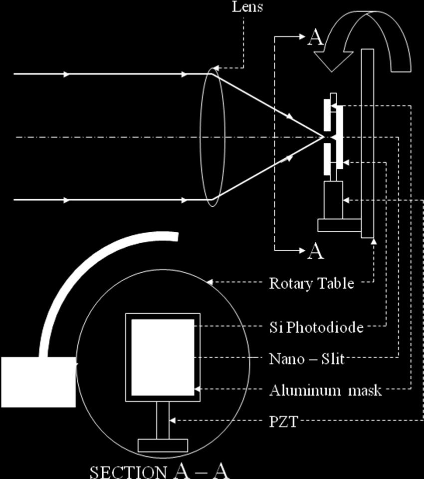
111 111 Fig
112 112 (a) (b) Fig 4. 23
113 113 (a) (b) (c) Fig
 Simulated scan data-point position error Fig. 6.")
114 114 (a) Simulated DC shift error between projections PDC (b) Simulated angular position error (c) Simulated scan data-point position error Fig
115 115 (a) Reconstruction with simulated DC shift error between projections PDC (b) Reconstruction with simulated angular position error (c) Reconstruction with simulated scan data-point position error Fig
116 116 (a) (b) Fig
![y [ m] y [ m] 117-5 Best focus 0.](/docs-images/73/69394236/images/117-0.jpg "75 Best focus 0 0.5 0.")
![25 5 0-5 0 5 x [ m] (a) Experiment](/docs-images/73/69394236/images/117-1.jpg "(b) Simulation -5 +20 um defocus")

117 y [ m] y [ m] Best focus 0.75 Best focus x [ m] (a) Experiment (b) Simulation um defocus +20 um defocus x [ m] (c) Experiment (d) Simulation Fig
118 [ m] y [ m] [ m] y [ m] [degrees] (a) Experimental Sinogram x [ m] (b) Experimental Reconstruction [degrees] x [ m] (c) Simulated Sinogram (d) Simulated Reconstruction Fig
119 119 (a) Simulated Object Features (b) Simulated Reconstructions Fig
120 120 APPENDIX C MANUSCRIPT: HIGH NA, PARTIALLY COHERENT TOMOGRAPHIC IMAGE RECONSTRUCTION USING A SCANNING NANO-SLIT The following manuscript has being submitted for review to Journal of the Optical Society of America A in February 2011.
121 121 High NA partially coherent tomographic image reconstruction using a scanning nano-slit Anoop George and Tom D. Milster College of Optical Sciences, University of Arizona, Tucson, Arizona 85721, USA Imaging characteristics of a scanning nano-slit sensor are determined for high NA partially coherent images. Good imaging performance (contrast > 0.8) is demonstrated with line-and-space images down to a spatial frequency of 2.38 lp / m. Sub-micron features in a high NA partially coherent image are measured with a scanning and rotating nano-slit. A modified microscope is used to create the measured features, including 210 nm half-pitch features that cannot be imaged using the microscope in a conventional imaging mode. Using a filtered back projection technique, two-dimensional sub-micron features are reconstructed by the nano-slit sensor. It is determined that the resolution limit is determined by the reconstruction technique and not by the width of the nano-slit. The nano-slit is 125 nm wide and 50 m long and is fabricated on a 120 nm thick layer of aluminum. OCIS codes: , , ,
122 INTRODUCTION Measuring nano-meter size irradiance features is of critical importance in industrial and research applications. This study presents measurement of various features on the order of a few 100 nm created by high NA partially coherent imaging. Features are measured by scanning a relatively long (50 m) and narrow (125 nm) nano-slit over a plane. The nano-slit provides direct measurement of irradiance at the plane of interest for the submicron features. A tomographic technique is used to reconstruct detailed twodimensional feature distributions. One technique to resolve sub micron irradiance features is by using a scanning near-field optical microscope (SNOM), which is also referred to as near-field scanning optical microscope (NSOM), in the collection mode [1-5]. The most common SNOM technique is to scan sub-micron apertures over the object in a linear raster pattern and record the transmitted power through the aperture as a function scan position. Apart from circular holes, apertures of varying shapes, including slits, have been used for SNOM applications [6]. Theoretical studies on the performance of slit apertures for SNOM applications have been studied, and their suitability has been established [7,8]. An experimental study has been performed on an SNOM with a 80 nm wide slit and images with features as small as 110 nm wide were resolved using the linear raster scan technique [9], but contrasts of the measured features were not provided. According to this study, a slit used in the linear scanning technique only resolved features well that were aligned parallel to the slit. Features orthogonal to the slit are poorly resolved with the limit of resolution being 2
123 123 poorer than 230 nm in this study [9]. Resolution of the SNOM is limited by the aperture size, which is typically 100 nm in diameter or less. These small apertures limit the power transmitted through them and hence limit the signal-to-noise ratio (SNR) of the measurement system. A study using coherent laser illumination determined that a scanning and rotating nanoslit aperture combined with tomographic filtered back-projection is capable of measuring sub-micron features [10]. The advantages of the tomographic nano-slit reconstruction technique over the SNOM technique is the possibility of improved SNR. The smallest resolvable feature is determined by the width of the slit, which could be as small as the state-of-the art SNOM aperture diameter. However, the slit could be considerably longer (on the order of a few m) and theoretically as long as the required field-of-view. This increased transmission area would significantly increase the light transmission through the aperture and hence improve SNR. The 125 nm wide, 50 m long nano-slit in this study is fabricated using focused ion beam (FIB) milling on a 120 nm thick layer of aluminum that is coated on a 500 m thick glass substrate. Figure 1 shows scanning electron microscope (SEM) images of the slit. Using line-and-space images, it was shown that this nano-slit is capable of imaging a 167 nm half-pitch feature with a contrast of ~ 0.9 [11]. Coherent sub-micron features were measured and simulations indicated that 200 nm Rayleigh resolution is possible with an infinitely narrow slit [10]. 3
124 124 In the previous studies using the same slit, only coherent illumination is used. In order for the nano-slit sensor to be used as a versatile image sensor, its performance is analyzed using partially coherent and incoherent illumination. Also, most current sub-micron imaging techniques employ a high NA. As such, the characteristics of the nano-slit when using high NA imaging is of considerable interest. This study takes into account the above mentioned factors and determines the ultimate resolution and contrast of the scanning and rotating nano-slit image sensor. An explanation of the tomographic method used in this study is outlined in Section 2. The experimental setup conditions are presented in Section 3. Section 4 presents results from modulation transfer function (MTF) studies, which is followed by results and analysis of the image reconstruction in Section 5. Section 6 lists conclusions from this work. 2. METHOD The measurement procedure for image reconstruction involves scanning the nano-slit over the aerial image pattern and recording power transmitted through the slit as a function of slit translation. At each position of the slit, recorded power is proportional to the line integral of the irradiance pattern along the length of the slit. A plot of power as a function of translation provides an integrated projection of the irradiance pattern in the direction orthogonal to slit translation. The slit angle is then varied, and the above procedure is repeated. Figure 2 shows a schematic of an irradiance pattern distribution and two projections Pm (, m ) and Pn (, n ) at angles m and n, respectively. A set 4
125 125 of projections is measured over 180 0, and an inverse Radon transform is performed to reconstruct the irradiance pattern. The inverse Radon transform is given by 2 I ( x, y) d d P(, )exp[ j2 (cos sin )], (2) 0 0 where I ( x, y) is the reconstructed irradiance pattern, P (, ) is the projection at an angle and is the spatial variable along the direction of slit translation. The principle used in this study is very similar to filtered back projection employed in computer-aided tomography (CAT) [12], where lateral and angular sampling intervals should satisfy the Nyquist criteria [12]. For a 5 m slit translation, 40 linear samples and 63 angular samples are required. An earlier study with the same instrument has a detailed description of the sampling requirements in this experiment [10]. 3. EXPERIMENT An upright Olympus microscope is used to obtain the required sub-micron feature sizes. The illumination / imaging path is modified, as shown in Fig. 3, with an object mask containing features larger than 1 m that is demagnified at the image plane of the objective lens. Measurement of this image-plane irradiance distribution is the goal of the study. Two experiments are performed. The first experiment measures MTFs of the system using sub-micron image features with different partial coherence conditions and numerical apertures (NA). The second experiment involves reconstructing a high NA, incoherent image with 300 nm half pitch-features. 5
126 126 The illumination source is a 7 mm 9 mm Light Emitting Diode (LED) (Superbright LED CREE XP XLamp) with a wavelength = 615 nm. The collector lens forms the first image of the source at the circular iris. The plane of the iris is reimaged onto the aperture stop location at the objective lens, as shown in Fig. 3. The partial coherence of the imaging system is controlled by adjusting the diameter of the source image at the stop as a function of the stop diameter [13]. The partial coherence is defined as D source image c, (1) D aperture stop where c is the partial coherence factor, D is the diameter of the image of the source image source at the aperture stop and D is the diameter of the stop. The LED source, aperture stop and hence its image, is square in shape. An iris at the first source image controls D source image at the stop. For all values of c used in the experiments, the open area of the circular iris lies inside the square source image. A field stop is placed at a distance of one focal length after the collector lens and defines the field-of-view of the measured image. The field stop is reimaged onto the object plane, where objects with micron size features are placed. The object and the image of the field stop are then reimaged (and demagnified) by the tube lens / objective lens combination to the image plane, where it is studied by the nano-slit sensor. For MTF measurements, a 50% duty cycle grating with 25 m half pitch is positioned at the object location. To generate different image spatial frequencies, four objective lenses with different magnifications are used. The objectives used have magnifications of 20 (Olympus UPlanFL - 20 / 0.50NA), 50 (Olympus LMPlanFL - 50 / 0.50NA), 100 6
127 127 (Olympus LMPlanFL / 0.80NA) and 150 (Olympus UPlanApo / 0.90NA), With a magnification of 0.090, 0.036,0.018 and and an object with a 25 m half pitch, the objectives create images with half pitches of 2250 nm, 900 nm, 450 nm and 300 nm, respectively at the image plane. Figure 4a shows the magnified aerial irradiance using a 300 nm half pitch image taken with a CCD camera (optical path not shown in Fig.3). In order to measure the image using the nano-slit, the aluminum mask containing the slit element is positioned in the image plane. The Al mask is mounted on a 4 mm 4 mm silicon photodiode, as shown in Fig. 3. The Al mask/photodiode combination is attached to a piezo-electric transducer (PZT) with a strain gauge (Thorlab s model number PZS001). The PZT translates the slit in a direction orthogonal to the optical axis and orthogonal to the long axis of the slit. The strain-gauge electronics record the distance translated. As the PZT is translated in the direction of the grating vector, the power detected by the photodiode is measured at discrete intervals. The power transmitted as a function of translation distance provides the measured aerial image. Only one angular orientation of the nano-slit is used for this measurement. In the second experiment, a reticle and a resolution object is used to create feature sizes on the order of 300 nm to 200 nm half-pitch at the image plane. For these measurements, the slit-scanning setup is mounted on a rotary stage, which enables rotation in the x- y plane. The center of the slit is aligned with the mechanical axis of rotation by visually observing the displacement of the slit upon rotation under a microscope, where alignment 7
128 128 accuracy is about 2 m. The axis of rotation is aligned with the optical axis using an interferometric technique [14]. The interferometric alignment step is accurate to better than 100 nm. As the PZT is translated over a range of 5 m, the power detected by the photodiode is read out at discrete intervals. A total of N d = 300 samples are acquired for every projection. The rotary stage is then rotated over in steps of 1 0, and the above procedure is repeated to record multiple integrated projections. The lateral and angular sampling intervals satisfy Nyquist criteria [10, 12]. 4. MTF ANALYSIS This section details analysis of results from the first experiment, which involves determining MTF by scanning aerial images with 2250 nm, 900 nm, 600 nm, 450 nm and 300 nm half-pitch features. Figure 4b shows a measurement using a 300 nm halfpitch image. Contrast of the image is defined as C P P ) /( P P ), (2) ( max min max min where P max and P min are the maximum and minimum powers recorded by the detector as the slit is translated over the image and C is the contrast (visibility) of the measured fringes. Contrast is measured for each of the four feature sizes (spatial frequencies) with partial coherence values of c = 1, 0.5 and 0.1. Figure 5 shows the measured contrast values plotted as a function of spatial frequency and partial coherence for 300 nm and 600 nm half-pitch features using a 0.9 NA objective lens. Theoretical MTF plots for a 0.9 8
129 129 NA objective lens at c = 1, 0.5 and 0.1 is plotted over the measured contrast values. According to [15, 16], the theoretical MTF values are calculated by 2 MTFObjective c, 0 NA/ 1, (3) MTF Objective 2 c [ 2 c cos cos ((( NA/ ) 1 1 ((( NA/ ) [1 ((( NA/ ) ((( NA/ ) c 2 c 2 c 2 c 1) /(2NA / )) -[((( NA/ ) 1) /(2NA/ )) 1) /(2NA/ )) -[((( NA/ ) 1) /(2NA/ )) ] c ] 2 1/ 2 2 1/ 2 where NA is the numerical aperture of the objective lens. ] ] 2 2 c 2 2 c 1) /(2NA/ )) 1 NA/ 1, c 1) /(2NA/ )) c The 300 nm half-pitch feature has a contrast between 0.35 and 0.25, depending on the partial coherence. It can be seen from Fig. 5 that the measured values for the three coherence factors lie within 12% of the theoretical value. For the 600 nm half-pitch feature, the errors between theoretical and measured contrast are 5%, 17% and 7% for c = 1, 0.5 and 0.1, respectively. Hence, the measured contrast agrees reasonably well with the theoretical calculations. The measured contrast values for three other spatial frequencies created using objectives with NA = 0.9, 0.8 and 0.5 are shown in Table 1. Theoretical MTF values for the different objectives are provided for comparison. It is seen that, even with incoherent imaging and a 0.9 NA objective lens, the nano-slit imaging system is capable of measuring images with theoretically expected contrasts for most spatial frequencies. Among all the spatial frequencies studied, the worst agreement between theoretical and measured contrast is 17% for a half-pitch of 600 nm and c = 0.5. Some of the measured 9
130 130 contrast values are greater than the theoretical values. For example, the largest increase in measured contrast over the theoretical value is 15% (corresponding to a 900 nm halfpitch feature and c = 1). This value is possible, because the theoretical MTF of the objective could be higher than that provided by Eq. 4, because the theoretical values provided by Eq. 4 are valid only for a sinusoidal image. For a square wave grating object, such as the one used in this study, the theoretical values are slightly higher, as discussed by Boreman [17]. According to Boreman, for a 900 nm half-pitch feature at c = 1, NA = 0.9 and =615 nm, the contrast for a square wave image is 25% greater than the contrast for a sinusoidal image. Hence, a 15% increase in measured contrast over the theoretical MTF value of a sinusoidal image is possible. Contrast is analyzed as a function of two orientations of linear polarization, as shown in Fig. 6. Regardless of the coherence factor or feature size, contrast is higher when the polarization is aligned parallel to the long axis of the slit (transverse electric - TE). When the polarization is aligned perpendicular to the long axis of the slit (transverse magnetic - TM), the contrast is lower. A similar scenario is seen in a previous work with the same slit using coherent illumination [11]. In the TM case, there is considerable evanescent radiation on the surface of the Al layer. The reason for the reduced contrast in the TM case is attributed to the presence of defects on the surface of the Al layer which convert some of the evanescent energy into propagating energy which is collected by the detector. The presence of these propagating waves increases the minimum transmitted power through the slit P min which in turn, according to Eq. 2, decreases the contrast. 10
131 IMAGE RECONSTRUCTION This section presents and analyzes images reconstructed using the scanning nano-slit in a tomographic mode. The first feature to be studied is a 300 nm wide isolated line feature formed using a 0.9 NA objective and c = 1. Figure 7 shows the magnified irradiance of the feature along with the field stop, as captured by a CCD camera. Also seen in the same figure is a section of the nano-slit. The diameter of the field stop is adjusted so that the diameter of the illumination area (4.8 m) is slightly smaller than the scan range (5 m). The experiment collects projection data of the image to form a sinogram. An inverse radon transform on the sinogram recreates the image, which is shown in Figure 8a. The inverse radon transform is implemented using the iradon function in MATLAB. A Ram-Lak filter in combination with Hamming filter is used in the reconstruction. The filtering process accentuates any high frequency noise in the image. This accentuation is controlled by truncating the filter at high spatial frequencies. No other pre-filtering of scan data (like averaging) is used in the reconstruction. A cross-section of the reconstructed image, as shown in Fig. 8b, shows the reconstructed feature to be ~ 500 nm at its widest point in the cross-section with a contrast of The increase in width of the 300 nm wide feature to ~ 500 nm is consistent with the findings of a previous study, which determined that a feature with an infinite-slope edge results in smoothing of the edges upon performing the tomographic action with the nano-slit [10]. Regardless of the 11
132 132 size of the feature, the edge is smoothed out ~ 210 nm over a 10% 90% irradiance threshold. There is some random noise in Fig. 7 and in the reconstruction shown in Fig 8a. Simulation studies are performed to determine the effect of this noise. Figure 9a shows a simulated feature with random noise similar to the aerial image used in the experiment (Fig.7). The noise is 15% of the maximum signal value. A MATLAB program calculates the sinogram using the noisy data assuming an infinitely narrow slit. Then, an inverse radon transform is performed on the sinogram to recreate the simulated image, which is shown in Fig. 9b. The simulated reconstruction in Fig. 9b shows a noisy image similar to that seen in Fig. 8a. Random noise in the measured experimental image could be one of the reasons for noise in the reconstructed image. Apart from a noisy aerial image, the reconstruction technique itself results in recreations with additional noise [12]. In order to study smaller features, a United States Air Force (USAF) resolution target is used as an object. However, due to the small field-of-view, only one spatial frequency pattern is studied at a time. Figure 10a shows a ~3.3 m ~1.7 m section corresponding to Group 4 and Element 6 on the object target. The half-pitch of each line in the object is 17.5 m. A 0.9 NA objective and c = 1 is used in the formation of the aerial image. The aerial image of the target at the slit plane is magnified and observed on a CCD, as shown in Fig 10b. The half-pitch of each line in the aerial image is 210 nm. The lines are not resolvable. Reconstruction of the aerial image using the nano-slit technique is shown in Fig. 10c. The reconstructed lines are resolvable with an average 12
133 133 contrast of 0.28 for the six 200 nm half-pitch features. The reconstructed image is noisy, because of the presence of noise in the measured aerial image itself and the inherent noise in the reconstruction technique. A different region of the USAF resolution target (corresponding to Group 5 and Element 3) is also tested. The half-pitch of each line in the aerial image is 148 nm. This feature could not be resolved using the nano-slit measurement technique. Hence, the ultimate resolution of the tomographic nano-slit measurement technique is ~ 200 nm. 6. CONCLUSIONS A 125 nm scanning and rotating nano-slit is used as an imaging device to directly measure high NA partially coherent sub-micron features. The nano-slit is placed in the plane of an aerial image with sub-micron features. Integrated projections, arranged to form sinograms, are obtained by experimentally scanning and rotating the nano-slit. A filtered back projection algorithm, like the ones used in CAT, is applied to the projections to recreate the images. Initially, line-and-space images are used to determine the characteristics of the nano-slit for imaging high NA partially coherent features. In this portion of the study only linear slit-scanning is employed. It is demonstrated that, even with incoherent imaging and a 0.9 NA objective lens, the nano-slit imaging system is capable of measuring images with theoretically expected contrasts for most spatial frequencies studied. This result supports a previous FDTD simulation study which indicates that, even with incoherent 13
134 134 illumination at a maximum illumination angle of 53 degree (NA = 0.8), the measured contrast is above 0.85 [10]. Effects of polarization on imaging are studied, and it was found that TE polarization scans have a higher contrast than TM polarization scans. This result is similar to that of a previous study undertaken with coherent illumination [11]. The second experiment involves reconstruction of high NA partially coherent images with a scanning and rotating nano-slit. Isolated and dense features are studied, and the best resolution obtained is 210 nm half-pitch. The 210 nm half-pitch feature is not resolved using conventional microscopic imaging. Sources of noise in the reconstruction are identified and presented. The nano-slit sensor is not capable of resolving adjacent features smaller than 210 nm half-pitch. This result validates an earlier simulation work [10] which determined 200 nm to be the resolution limit by scanning and rotating a infinitely narrow slit. This work demonstrates that for an arbitrary image the scanning and rotating nano-slit technique is capable of reconstructing features that could not be resolved with conventional microscopy under equivalent illumination conditions. For a slit with a width less than 125 nm, the reconstruction technique limits the resolution to ~ 200 nm halfpitch. 14
135 ACKNOWLEDGEMENTS The authors thank Veeco for facilitating the use of the Wyko NT9800 surface profiler, which helped immensely with aligning the slit element and analyzing nano-meter scale features and Grant Baumgardner of Arizona State University for fabricating the nano-slit. 15
136 136 REFERENCES 1. E.A. Ash and G. Nicholls, Super-resolution Aperture Scanning Microscope, Nature, Vol. 237, pp (1972). 2. E. Betzig, M. Isaacson, H. Barshatzky, A. Lewis and K. Lin, Super-resolution imaging with near-field scanning optical microscopy (NSOM), Ultramicroscopy, Vol. 25, Issue 2, pp (1988) 3. B. Hecht, B. Sick, U.P. Wild, V. Deckert, R. Zenobi, O.J.F. Martin and D.W. Pohl, Scanning near-field optical microscopy with aperture probes: Fundamentals and applications, The Journal of Chemical Physics, Vol. 112, No. 18, pp (2000). 4. E.L. Buckland, P.J. Moyer and M.A. Paesler, Resolution in collection-mode scanning optical microscopy, J. Appl. Phys., Vol. 73, No. 3, pp (1993). 5. E. Betzig, M. Isaacson and A. Lewis, Collection mode near-field scanning optical microscopy, Appl. Phys. Lett., Vol. 51, No. 25, pp (1987). 6. E.X. Jin and X. Xu, Focussed ion beam machined cantilever aperture probes for near-field optical imaging, Journal of Microscopy, Vol. 229, Pt. 3, pp (2008). 7. L. Novotny, D.W. Pohl and P. Regli, Near-field, far-field and imaging properties of the 2D aperture SNOM, Ultramicroscopy, Vol. 57, pp (1995) 16
137 E. Betzig, A. Harootunian, A. Lewis and M. Isaacson, Near-field diffraction by a slit: implications for superresolution microscopy, Applied Optics, Vol. 25, No. 12, pp (1986) 9. H.U. Danzebrink, T.H. Dziomba, T. Sulzbach, O. Ohlsson, C. Lehrer and L. Frey, Nano-slit probes for near-field optical microscopy fabricated by focused ion beams, Journal of Microscopy, Vol. 194, Pt. 2/3, pp , (1999). 10. A. George and T.D. Milster, Spot distribution measurement using a scanning nano-slit, Submitted for review to Applied Optics (2011) 11. A. George and T.D. Milster, Characteristics of a Scanning Nano-Slit Image Sensor for Line-and-Space Patterns, Applied Optics, Vol. 49 Issue 19, pp (2010) 12 H.H. Barrett and W. Swindell, Radiological Imaging: The Theory of Image Formation, Detection, and Processing - Volume 2, Academic Press, New York, pp (1981) 13 A.K. Wong, Resolution Enhancement Techniques in Optical Lithography, SPIE The International Society for optical Engineering, Bellingham, pp (2001) 14 T.D. Milster and C.L. Vernold,, Technique for aligning optical and mechanical axes based on a rotating linear grating, Optical Engineering, Vol. 34 Issue 10, pp (1995) 15 C.J.R. Sheppard, Diffused transfer function for a partially coherent microscope and application to phase retrieval, J. Opt. Soc. Am. A, Vol. 21, No. 5, pp (2004) 17
138 H.H. Hopkins, On the diffraction theory of optical images, Proc. R. Soc. Lond. A, Vol. 217, pp (1953) 17 G.D. Boreman, Handbook of Optics: Transfer Function Techniques (Chapter 2), 3 rd Edition, McGraw-Hill, New York, pp
139 139 FIGURE CAPTIONS Fig. 1. The 125 nm wide slit fabricated on a 110 nm thick aluminum mask. The aluminum is deposited on a glass substrate. The length of the slit into the plane of the drawing is 50 m. (a) top view (b) cross-section. Fig 2. Schematic for the method employed in reconstructing an aerial image. Shown are the aerial image and two random projections P m (, ) and P n (, ) at angles m and n, respectively. Multiple projections are arranged to form a sonogram, which is then analyzed with an inverse radon transform to recreate the irradiance distribution. The technique is similar to that used in computer aided tomography (CAT) [12]. Fig. 3. Schematic of the experimental setup. The illumination path is such that the image of the source is conjugate to the iris and the aperture stop at the objective lens. In the imaging path, the field stop is conjugate to the object and the image plane of the objective lens. Fig.4. (a) The magnified image of a binary grating with 300 nm half pitch features to be measured using the nano-slit sensor. The image is formed by a by a 0.9 NA objective and c =1. The image is taken with a CCD camera connected to the microscope, and contrast is enhanced for clarity. (b) Measured 300 nm half-pitch image formed by a 0.9 NA objective and c =1. The contrast of this image is 0.37 using the nano-slit and 0.24 using the unenhanced CCD camera image. 19
140 140 Fig 5. Experimentally obtained contrast values plotted as a function of spatial frequency and partial coherence. The two spatial frequencies of interest lp/ m (300 nm half pitch) and lp/ m (600 nm half pitch) are both created with a 0.9 NA objective. The three curves represent the 0.9 NA theoretical MTF plots for different partial coherence factors. Symbols indicate experimental values and contains error bar. Fig. 6. Change in contrast as a function of illumination polarization for a 900 nm halfpitch feature and a 300 nm half-pitch feature. Linear polarization is used at the object plane. The contrast is higher when the direction of polarization is along the long axis of the slit, TE (0 0 and ). The contrast is lowest when the direction of polarization is orthogonal to the long axis of the slit, TM (90 0 ). Fig. 7. Magnified image of a circular pupil (4.8 m diameter) with a 300 nm wide isolated line. The image is taken with a CCD camera connected to the microscope. The nano-slit is also seen at an angle to the feature. The slit is 125 nm wide at the center of its cross-sectional profile and is 285 nm wide at its widest part which is at the surface of the aluminum layer, as seen in Fig. 1. Fig. 8. (a) The reconstructed image of an isolated 300 nm line feature, obtained by performing an inverse radon transform on the measured projections. The power level in the reconstructed image is normalized to the maximum pixel power. (c) A cross-section 20
141 141 of the reconstructed image along the x-axis at y=0. The width of the reconstructed line at the widest part of its cross-sectional profile is ~ 500 nm and the contrast is ~ Fig 9. (a) Simulated image with a 300 nm wide isolated line and signal dependent noise as seen in the experiment (Fig. 7). The noise is 15% of the maximum signal value. (b) The reconstruction of the image obtained after simulating the effect of a scanning and rotating infinitely-narrow slit. Fig 10 (a) The USAF resolution target used as the object. A ~3.3 m ~1.7 m section is used corresponding to Group 4 and Element 6 on the target. The half-pitch of each line in the object is 17.5 m. (b) The image of the target at the slit plane, viewed under a microscope. The half-pitch of each line in the image is 210 nm and cannot be resolved. Image contrast is significantly enhanced in this section of the figure. (c) The reconstructed image, obtained by performing an inverse radon transform on the measured projections of the image shown in Fig 10b. The power level in the reconstructed image is normalized to the maximum pixel power. 21
142 142 Figure 1. 22
143 143 Figure 2. 23

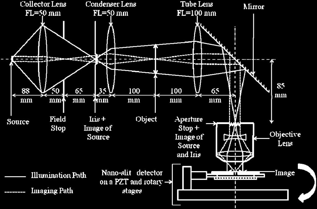
144 144 Figure 3. 24

145 145 Relative Signal X (a) P max X P min 0.2 Detector current using the nano-slit Image profile using the CCD camera Distance [nm] (b) Figure 4. 25
146 146 Contrast Half Pitch [nm] Theoretical MTF s =1 c s =0.5 c s =0.1 c C,s =1 meas c C,s =0.5 meas c C,s =0.1 meas c Spatial Frequency [1p/ m] Figure 5. 26
147 147 Half-Pitch s c 900 nm, nm nm nm Rotation of linear polarization with respect to the long axis of the slit [degrees] Figure 6. 27

148 nm wide line Image of Field Stop 125 nm wide slit 5 m Figure 7. 28
149 149 Normalized Power y [ m] x [ m] ~500 nm (a) (b) x [ m] Figure 8. 29

150 150 (a) (b) Figure 9. 30
![151 (a) 417 m (b) 5 m -2 1-1 0.8 y [ m] 0 0.6 0.](/docs-images/73/69394236/images/151-0.jpg "4 1 0.2 (c) 2 0-2 -1 0 1 2 x [ m] Figure 10. 31")
151 151 (a) 417 m (b) 5 m y [ m] (c) x [ m] Figure
Nanonics Systems are the Only SPMs that Allow for On-line Integration with Standard MicroRaman Geometries
 Nanonics Systems are the Only SPMs that Allow for On-line Integration with Standard MicroRaman Geometries 2002 Photonics Circle of Excellence Award PLC Ltd, England, a premier provider of Raman microspectral
attosnom I: Topography and Force Images NANOSCOPY APPLICATION NOTE M06 RELATED PRODUCTS G
 APPLICATION NOTE M06 attosnom I: Topography and Force Images Scanning near-field optical microscopy is the outstanding technique to simultaneously measure the topography and the optical contrast of a sample.
Investigation of the Near-field Distribution at Novel Nanometric Aperture Laser
 Investigation of the Near-field Distribution at Novel Nanometric Aperture Laser Tiejun Xu, Jia Wang, Liqun Sun, Jiying Xu, Qian Tian Presented at the th International Conference on Electronic Materials
Principles of Optics for Engineers
 Principles of Optics for Engineers Uniting historically different approaches by presenting optical analyses as solutions of Maxwell s equations, this unique book enables students and practicing engineers
Confocal Imaging Through Scattering Media with a Volume Holographic Filter
 Confocal Imaging Through Scattering Media with a Volume Holographic Filter Michal Balberg +, George Barbastathis*, Sergio Fantini % and David J. Brady University of Illinois at Urbana-Champaign, Urbana,
Fabrication of Probes for High Resolution Optical Microscopy
 Fabrication of Probes for High Resolution Optical Microscopy Physics 564 Applied Optics Professor Andrès La Rosa David Logan May 27, 2010 Abstract Near Field Scanning Optical Microscopy (NSOM) is a technique
Project Staff: Timothy A. Savas, Michael E. Walsh, Thomas B. O'Reilly, Dr. Mark L. Schattenburg, and Professor Henry I. Smith
 9. Interference Lithography Sponsors: National Science Foundation, DMR-0210321; Dupont Agreement 12/10/99 Project Staff: Timothy A. Savas, Michael E. Walsh, Thomas B. O'Reilly, Dr. Mark L. Schattenburg,
NSOM (SNOM) Overview
 Overview") NSOM (SNOM) Overview The limits of far field imaging In the early 1870s, Ernst Abbe formulated a rigorous criterion for being able to resolve two objects in a light microscope: d > ë / (2sinè) where d
NSOM (SNOM) Overview The limits of far field imaging In the early 1870s, Ernst Abbe formulated a rigorous criterion for being able to resolve two objects in a light microscope: d > ë / (2sinè) where d
Laser Beam Analysis Using Image Processing
 Journal of Computer Science 2 (): 09-3, 2006 ISSN 549-3636 Science Publications, 2006 Laser Beam Analysis Using Image Processing Yas A. Alsultanny Computer Science Department, Amman Arab University for
Optics and Lasers. Matt Young. Including Fibers and Optical Waveguides
 Matt Young Optics and Lasers Including Fibers and Optical Waveguides Fourth Revised Edition With 188 Figures Springer-Verlag Berlin Heidelberg New York London Paris Tokyo Hong Kong Barcelona Budapest Contents
EE119 Introduction to Optical Engineering Spring 2003 Final Exam. Name:
 EE119 Introduction to Optical Engineering Spring 2003 Final Exam Name: SID: CLOSED BOOK. THREE 8 1/2 X 11 SHEETS OF NOTES, AND SCIENTIFIC POCKET CALCULATOR PERMITTED. TIME ALLOTTED: 180 MINUTES Fundamental
R.B.V.R.R. WOMEN S COLLEGE (AUTONOMOUS) Narayanaguda, Hyderabad.
 Narayanaguda, Hyderabad.") R.B.V.R.R. WOMEN S COLLEGE (AUTONOMOUS) Narayanaguda, Hyderabad. DEPARTMENT OF PHYSICS QUESTION BANK FOR SEMESTER III PAPER III OPTICS UNIT I: 1. MATRIX METHODS IN PARAXIAL OPTICS 2. ABERATIONS UNIT II
R.B.V.R.R. WOMEN S COLLEGE (AUTONOMOUS) Narayanaguda, Hyderabad. DEPARTMENT OF PHYSICS QUESTION BANK FOR SEMESTER III PAPER III OPTICS UNIT I: 1. MATRIX METHODS IN PARAXIAL OPTICS 2. ABERATIONS UNIT II
Will contain image distance after raytrace Will contain image height after raytrace
 Name: LASR 51 Final Exam May 29, 2002 Answer all questions. Module numbers are for guidance, some material is from class handouts. Exam ends at 8:20 pm. Ynu Raytracing The first questions refer to the
TSBB09 Image Sensors 2018-HT2. Image Formation Part 1
 TSBB09 Image Sensors 2018-HT2 Image Formation Part 1 Basic physics Electromagnetic radiation consists of electromagnetic waves With energy That propagate through space The waves consist of transversal
2. Pulsed Acoustic Microscopy and Picosecond Ultrasonics
 1st International Symposium on Laser Ultrasonics: Science, Technology and Applications July 16-18 2008, Montreal, Canada Picosecond Ultrasonic Microscopy of Semiconductor Nanostructures Thomas J GRIMSLEY
Heisenberg) relation applied to space and transverse wavevector
 relation applied to space and transverse wavevector") 2. Optical Microscopy 2.1 Principles A microscope is in principle nothing else than a simple lens system for magnifying small objects. The first lens, called the objective, has a short focal length (a
2. Optical Microscopy 2.1 Principles A microscope is in principle nothing else than a simple lens system for magnifying small objects. The first lens, called the objective, has a short focal length (a
Imaging Systems Laboratory II. Laboratory 8: The Michelson Interferometer / Diffraction April 30 & May 02, 2002
 1051-232 Imaging Systems Laboratory II Laboratory 8: The Michelson Interferometer / Diffraction April 30 & May 02, 2002 Abstract. In the last lab, you saw that coherent light from two different locations
Study of shear force as a distance regulation mechanism for scanning near-field optical microscopy
 Study of shear force as a distance regulation mechanism for scanning near-field optical microscopy C. Durkan a) and I. V. Shvets Department of Physics, Trinity College Dublin, Ireland Received 31 May 1995;
Lithography. 3 rd. lecture: introduction. Prof. Yosi Shacham-Diamand. Fall 2004
 Lithography 3 rd lecture: introduction Prof. Yosi Shacham-Diamand Fall 2004 1 List of content Fundamental principles Characteristics parameters Exposure systems 2 Fundamental principles Aerial Image Exposure
Supplementary Figure 1 Reflective and refractive behaviors of light with normal
 Supplementary Figures Supplementary Figure 1 Reflective and refractive behaviors of light with normal incidence in a three layer system. E 1 and E r are the complex amplitudes of the incident wave and
Chapter 36: diffraction
 Chapter 36: diffraction Fresnel and Fraunhofer diffraction Diffraction from a single slit Intensity in the single slit pattern Multiple slits The Diffraction grating X-ray diffraction Circular apertures
Supplementary Figure 1. Effect of the spacer thickness on the resonance properties of the gold and silver metasurface layers.
 Supplementary Figure 1. Effect of the spacer thickness on the resonance properties of the gold and silver metasurface layers. Finite-difference time-domain calculations of the optical transmittance through
Characteristics of point-focus Simultaneous Spatial and temporal Focusing (SSTF) as a two-photon excited fluorescence microscopy
 as a two-photon excited fluorescence microscopy") Characteristics of point-focus Simultaneous Spatial and temporal Focusing (SSTF) as a two-photon excited fluorescence microscopy Qiyuan Song (M2) and Aoi Nakamura (B4) Abstracts: We theoretically and experimentally
Characteristics of point-focus Simultaneous Spatial and temporal Focusing (SSTF) as a two-photon excited fluorescence microscopy Qiyuan Song (M2) and Aoi Nakamura (B4) Abstracts: We theoretically and experimentally
A broadband achromatic metalens for focusing and imaging in the visible
 SUPPLEMENTARY INFORMATION Articles https://doi.org/10.1038/s41565-017-0034-6 In the format provided by the authors and unedited. A broadband achromatic metalens for focusing and imaging in the visible
CHAPTER 2 POLARIZATION SPLITTER- ROTATOR BASED ON A DOUBLE- ETCHED DIRECTIONAL COUPLER
 CHAPTER 2 POLARIZATION SPLITTER- ROTATOR BASED ON A DOUBLE- ETCHED DIRECTIONAL COUPLER As we discussed in chapter 1, silicon photonics has received much attention in the last decade. The main reason is
Applications of Optics
 Nicholas J. Giordano www.cengage.com/physics/giordano Chapter 26 Applications of Optics Marilyn Akins, PhD Broome Community College Applications of Optics Many devices are based on the principles of optics
attocfm I for Surface Quality Inspection NANOSCOPY APPLICATION NOTE M01 RELATED PRODUCTS G
 APPLICATION NOTE M01 attocfm I for Surface Quality Inspection Confocal microscopes work by scanning a tiny light spot on a sample and by measuring the scattered light in the illuminated volume. First,
Digital Camera Technologies for Scientific Bio-Imaging. Part 2: Sampling and Signal
 Digital Camera Technologies for Scientific Bio-Imaging. Part 2: Sampling and Signal Yashvinder Sabharwal, 1 James Joubert 2 and Deepak Sharma 2 1. Solexis Advisors LLC, Austin, TX, USA 2. Photometrics
1.6 Beam Wander vs. Image Jitter
 8 Chapter 1 1.6 Beam Wander vs. Image Jitter It is common at this point to look at beam wander and image jitter and ask what differentiates them. Consider a cooperative optical communication system that
Chapter 17: Wave Optics. What is Light? The Models of Light 1/11/13
 Chapter 17: Wave Optics Key Terms Wave model Ray model Diffraction Refraction Fringe spacing Diffraction grating Thin-film interference What is Light? Light is the chameleon of the physical world. Under
ECEN 4606, UNDERGRADUATE OPTICS LAB
 ECEN 4606, UNDERGRADUATE OPTICS LAB Lab 3: Imaging 2 the Microscope Original Version: Professor McLeod SUMMARY: In this lab you will become familiar with the use of one or more lenses to create highly
A process for, and optical performance of, a low cost Wire Grid Polarizer
 1.0 Introduction A process for, and optical performance of, a low cost Wire Grid Polarizer M.P.C.Watts, M. Little, E. Egan, A. Hochbaum, Chad Jones, S. Stephansen Agoura Technology Low angle shadowed deposition
Development of a new multi-wavelength confocal surface profilometer for in-situ automatic optical inspection (AOI)
") Development of a new multi-wavelength confocal surface profilometer for in-situ automatic optical inspection (AOI) Liang-Chia Chen 1#, Chao-Nan Chen 1 and Yi-Wei Chang 1 1. Institute of Automation Technology,
Development of a new multi-wavelength confocal surface profilometer for in-situ automatic optical inspection (AOI) Liang-Chia Chen 1#, Chao-Nan Chen 1 and Yi-Wei Chang 1 1. Institute of Automation Technology,
Synthesis of projection lithography for low k1 via interferometry
 Synthesis of projection lithography for low k1 via interferometry Frank Cropanese *, Anatoly Bourov, Yongfa Fan, Andrew Estroff, Lena Zavyalova, Bruce W. Smith Center for Nanolithography Research, Rochester
Experiment 1: Fraunhofer Diffraction of Light by a Single Slit
 Experiment 1: Fraunhofer Diffraction of Light by a Single Slit Purpose 1. To understand the theory of Fraunhofer diffraction of light at a single slit and at a circular aperture; 2. To learn how to measure
Chapter Ray and Wave Optics
 109 Chapter Ray and Wave Optics 1. An astronomical telescope has a large aperture to [2002] reduce spherical aberration have high resolution increase span of observation have low dispersion. 2. If two
Use of Computer Generated Holograms for Testing Aspheric Optics
 Use of Computer Generated Holograms for Testing Aspheric Optics James H. Burge and James C. Wyant Optical Sciences Center, University of Arizona, Tucson, AZ 85721 http://www.optics.arizona.edu/jcwyant,
Optical transfer function shaping and depth of focus by using a phase only filter
 Optical transfer function shaping and depth of focus by using a phase only filter Dina Elkind, Zeev Zalevsky, Uriel Levy, and David Mendlovic The design of a desired optical transfer function OTF is a
OCT Spectrometer Design Understanding roll-off to achieve the clearest images
 OCT Spectrometer Design Understanding roll-off to achieve the clearest images Building a high-performance spectrometer for OCT imaging requires a deep understanding of the finer points of both OCT theory
NanoSpective, Inc Progress Drive Suite 137 Orlando, Florida
 TEM Techniques Summary The TEM is an analytical instrument in which a thin membrane (typically < 100nm) is placed in the path of an energetic and highly coherent beam of electrons. Typical operating voltages
Optical Coherence: Recreation of the Experiment of Thompson and Wolf
 Optical Coherence: Recreation of the Experiment of Thompson and Wolf David Collins Senior project Department of Physics, California Polytechnic State University San Luis Obispo June 2010 Abstract The purpose
Application Note #548 AcuityXR Technology Significantly Enhances Lateral Resolution of White-Light Optical Profilers
 Application Note #548 AcuityXR Technology Significantly Enhances Lateral Resolution of White-Light Optical Profilers ContourGT with AcuityXR TM capability White light interferometry is firmly established
HIGH RESOLUTION COMPUTERIZED TOMOGRAPHY SYSTEM USING AN IMAGING PLATE
 HIGH RESOLUTION COMPUTERIZED TOMOGRAPHY SYSTEM USING AN IMAGING PLATE Takeyuki Hashimoto 1), Morio Onoe 2), Hiroshi Nakamura 3), Tamon Inouye 4), Hiromichi Jumonji 5), Iwao Takahashi 6); 1)Yokohama Soei
Design, Fabrication and Characterization of Very Small Aperture Lasers
 372 Progress In Electromagnetics Research Symposium 2005, Hangzhou, China, August 22-26 Design, Fabrication and Characterization of Very Small Aperture Lasers Jiying Xu, Jia Wang, and Qian Tian Tsinghua
Physics 431 Final Exam Examples (3:00-5:00 pm 12/16/2009) TIME ALLOTTED: 120 MINUTES Name: Signature:
 TIME ALLOTTED: 120 MINUTES Name: Signature:") Physics 431 Final Exam Examples (3:00-5:00 pm 12/16/2009) TIME ALLOTTED: 120 MINUTES Name: PID: Signature: CLOSED BOOK. TWO 8 1/2 X 11 SHEET OF NOTES (double sided is allowed), AND SCIENTIFIC POCKET CALCULATOR
Physics 431 Final Exam Examples (3:00-5:00 pm 12/16/2009) TIME ALLOTTED: 120 MINUTES Name: PID: Signature: CLOSED BOOK. TWO 8 1/2 X 11 SHEET OF NOTES (double sided is allowed), AND SCIENTIFIC POCKET CALCULATOR
Diffraction, Fourier Optics and Imaging
 1 Diffraction, Fourier Optics and Imaging 1.1 INTRODUCTION When wave fields pass through obstacles, their behavior cannot be simply described in terms of rays. For example, when a plane wave passes through
PH880 Topics in Physics
 PH880 Topics in Physics Modern Optical Imaging (Fall 2010) Overview of week 12 Monday: FRET Wednesday: NSOM Förster resonance energy transfer (FRET) Fluorescence emission i FRET Donor Acceptor wikipedia
X-RAY COMPUTED TOMOGRAPHY
 X-RAY COMPUTED TOMOGRAPHY Bc. Jan Kratochvíla Czech Technical University in Prague Faculty of Nuclear Sciences and Physical Engineering Abstract Computed tomography is a powerful tool for imaging the inner
The diffraction of light
 7 The diffraction of light 7.1 Introduction As introduced in Chapter 6, the reciprocal lattice is the basis upon which the geometry of X-ray and electron diffraction patterns can be most easily understood
Manufacturing Metrology Team
 The Team has a range of state-of-the-art equipment for the measurement of surface texture and form. We are happy to discuss potential measurement issues and collaborative research Manufacturing Metrology
Chapter 16 Light Waves and Color
 Chapter 16 Light Waves and Color Lecture PowerPoint Copyright The McGraw-Hill Companies, Inc. Permission required for reproduction or display. What causes color? What causes reflection? What causes color?
CHAPTER 2 MICROSTRIP REFLECTARRAY ANTENNA AND PERFORMANCE EVALUATION
 43 CHAPTER 2 MICROSTRIP REFLECTARRAY ANTENNA AND PERFORMANCE EVALUATION 2.1 INTRODUCTION This work begins with design of reflectarrays with conventional patches as unit cells for operation at Ku Band in
plasmonic nanoblock pair
 Nanostructured potential of optical trapping using a plasmonic nanoblock pair Yoshito Tanaka, Shogo Kaneda and Keiji Sasaki* Research Institute for Electronic Science, Hokkaido University, Sapporo 1-2,
Computer Generated Holograms for Optical Testing
 Computer Generated Holograms for Optical Testing Dr. Jim Burge Associate Professor Optical Sciences and Astronomy University of Arizona jburge@optics.arizona.edu 520-621-8182 Computer Generated Holograms
Introduction of New Products
 Field Emission Electron Microscope JEM-3100F For evaluation of materials in the fields of nanoscience and nanomaterials science, TEM is required to provide resolution and analytical capabilities that can
Spatially Resolved Backscatter Ceilometer
 Spatially Resolved Backscatter Ceilometer Design Team Hiba Fareed, Nicholas Paradiso, Evan Perillo, Michael Tahan Design Advisor Prof. Gregory Kowalski Sponsor, Spectral Sciences Inc. Steve Richstmeier,
Applications of Steady-state Multichannel Spectroscopy in the Visible and NIR Spectral Region
 Feature Article JY Division I nformation Optical Spectroscopy Applications of Steady-state Multichannel Spectroscopy in the Visible and NIR Spectral Region Raymond Pini, Salvatore Atzeni Abstract Multichannel
Criteria for Optical Systems: Optical Path Difference How do we determine the quality of a lens system? Several criteria used in optical design
 Criteria for Optical Systems: Optical Path Difference How do we determine the quality of a lens system? Several criteria used in optical design Computer Aided Design Several CAD tools use Ray Tracing (see
Tunable Color Filters Based on Metal-Insulator-Metal Resonators
 Chapter 6 Tunable Color Filters Based on Metal-Insulator-Metal Resonators 6.1 Introduction In this chapter, we discuss the culmination of Chapters 3, 4, and 5. We report a method for filtering white light
Observational Astronomy
 Observational Astronomy Instruments The telescope- instruments combination forms a tightly coupled system: Telescope = collecting photons and forming an image Instruments = registering and analyzing the
Properties of Structured Light
 Properties of Structured Light Gaussian Beams Structured light sources using lasers as the illumination source are governed by theories of Gaussian beams. Unlike incoherent sources, coherent laser sources
Instructions for the Experiment
 Instructions for the Experiment Excitonic States in Atomically Thin Semiconductors 1. Introduction Alongside with electrical measurements, optical measurements are an indispensable tool for the study of
Near-field Optical Microscopy
 Near-field Optical Microscopy R. Fernandez, X. Wang, N. Li, K. Parker, and A. La Rosa Physics Department Portland State University Portland, Oregon Near-Field SPIE Optics Microscopy East 2005 Group PSU
Physics 3340 Spring Fourier Optics
 Physics 3340 Spring 011 Purpose Fourier Optics In this experiment we will show how the Fraunhofer diffraction pattern or spatial Fourier transform of an object can be observed within an optical system.
FRAUNHOFER AND FRESNEL DIFFRACTION IN ONE DIMENSION
 FRAUNHOFER AND FRESNEL DIFFRACTION IN ONE DIMENSION Revised November 15, 2017 INTRODUCTION The simplest and most commonly described examples of diffraction and interference from two-dimensional apertures
SUPPLEMENTARY INFORMATION
 SUPPLEMENTARY INFORMATION DOI: 10.1038/NNANO.2015.137 Controlled steering of Cherenkov surface plasmon wakes with a one-dimensional metamaterial Patrice Genevet *, Daniel Wintz *, Antonio Ambrosio *, Alan
Resolution. [from the New Merriam-Webster Dictionary, 1989 ed.]:
![Resolution. [from the New Merriam-Webster Dictionary, 1989 ed.]:](/thumbs/71/66141426.jpg "Resolution. [from the New Merriam-Webster Dictionary, 1989 ed.]:") Resolution [from the New Merriam-Webster Dictionary, 1989 ed.]: resolve v : 1 to break up into constituent parts: ANALYZE; 2 to find an answer to : SOLVE; 3 DETERMINE, DECIDE; 4 to make or pass a formal
Resolution [from the New Merriam-Webster Dictionary, 1989 ed.]: resolve v : 1 to break up into constituent parts: ANALYZE; 2 to find an answer to : SOLVE; 3 DETERMINE, DECIDE; 4 to make or pass a formal
EE119 Introduction to Optical Engineering Fall 2009 Final Exam. Name:
 EE119 Introduction to Optical Engineering Fall 2009 Final Exam Name: SID: CLOSED BOOK. THREE 8 1/2 X 11 SHEETS OF NOTES, AND SCIENTIFIC POCKET CALCULATOR PERMITTED. TIME ALLOTTED: 180 MINUTES Fundamental
Reducing Proximity Effects in Optical Lithography
 INTERFACE '96 This paper was published in the proceedings of the Olin Microlithography Seminar, Interface '96, pp. 325-336. It is made available as an electronic reprint with permission of Olin Microelectronic
LOS 1 LASER OPTICS SET
 LOS 1 LASER OPTICS SET Contents 1 Introduction 3 2 Light interference 5 2.1 Light interference on a thin glass plate 6 2.2 Michelson s interferometer 7 3 Light diffraction 13 3.1 Light diffraction on a
N.N.Soboleva, S.M.Kozel, G.R.Lockshin, MA. Entin, K.V. Galichsky, P.L. Lebedinsky, P.M. Zhdanovich. Moscow Institute ofphysics and Technology
 Computer assisted optics teaching at the Moscow Institute ofphysics and Technology N.N.Soboleva, S.M.Kozel, G.R.Lockshin, MA. Entin, K.V. Galichsky, P.L. Lebedinsky, P.M. Zhdanovich Moscow Institute ofphysics
INTRODUCTION THIN LENSES. Introduction. given by the paraxial refraction equation derived last lecture: Thin lenses (19.1) = 1. Double-lens systems
 = 1. Double-lens systems") Chapter 9 OPTICAL INSTRUMENTS Introduction Thin lenses Double-lens systems Aberrations Camera Human eye Compound microscope Summary INTRODUCTION Knowledge of geometrical optics, diffraction and interference,
Chapter 9 OPTICAL INSTRUMENTS Introduction Thin lenses Double-lens systems Aberrations Camera Human eye Compound microscope Summary INTRODUCTION Knowledge of geometrical optics, diffraction and interference,
Improving the Collection Efficiency of Raman Scattering
 PERFORMANCE Unparalleled signal-to-noise ratio with diffraction-limited spectral and imaging resolution Deep-cooled CCD with excelon sensor technology Aberration-free optical design for uniform high resolution
End-of-Chapter Exercises
 End-of-Chapter Exercises Exercises 1 12 are conceptual questions designed to see whether you understand the main concepts in the chapter. 1. Red laser light shines on a double slit, creating a pattern
Investigation of an optical sensor for small angle detection
 Investigation of an optical sensor for small angle detection usuke Saito, oshikazu rai and Wei Gao Nano-Metrology and Control Lab epartment of Nanomechanics Graduate School of Engineering, Tohoku University
ADVANCED OPTICS LAB -ECEN Basic Skills Lab
 ADVANCED OPTICS LAB -ECEN 5606 Basic Skills Lab Dr. Steve Cundiff and Edward McKenna, 1/15/04 Revised KW 1/15/06, 1/8/10 Revised CC and RZ 01/17/14 The goal of this lab is to provide you with practice
Εισαγωγική στην Οπτική Απεικόνιση
 Εισαγωγική στην Οπτική Απεικόνιση Δημήτριος Τζεράνης, Ph.D. Εμβιομηχανική και Βιοϊατρική Τεχνολογία Τμήμα Μηχανολόγων Μηχανικών Ε.Μ.Π. Χειμερινό Εξάμηνο 2015 Light: A type of EM Radiation EM radiation:
Difrotec Product & Services. Ultra high accuracy interferometry & custom optical solutions
 Difrotec Product & Services Ultra high accuracy interferometry & custom optical solutions Content 1. Overview 2. Interferometer D7 3. Benefits 4. Measurements 5. Specifications 6. Applications 7. Cases
ECEN. Spectroscopy. Lab 8. copy. constituents HOMEWORK PR. Figure. 1. Layout of. of the
 ECEN 4606 Lab 8 Spectroscopy SUMMARY: ROBLEM 1: Pedrotti 3 12-10. In this lab, you will design, build and test an optical spectrum analyzer and use it for both absorption and emission spectroscopy. The
Modulation Transfer Function
 Modulation Transfer Function The resolution and performance of an optical microscope can be characterized by a quantity known as the modulation transfer function (MTF), which is a measurement of the microscope's
ADVANCED OPTICS LAB -ECEN 5606
 ADVANCED OPTICS LAB -ECEN 5606 Basic Skills Lab Dr. Steve Cundiff and Edward McKenna, 1/15/04 rev KW 1/15/06, 1/8/10 The goal of this lab is to provide you with practice of some of the basic skills needed
Laser Telemetric System (Metrology)
") Laser Telemetric System (Metrology) Laser telemetric system is a non-contact gauge that measures with a collimated laser beam (Refer Fig. 10.26). It measure at the rate of 150 scans per second. It basically
Laser Telemetric System (Metrology) Laser telemetric system is a non-contact gauge that measures with a collimated laser beam (Refer Fig. 10.26). It measure at the rate of 150 scans per second. It basically
Waveguiding in PMMA photonic crystals
 ROMANIAN JOURNAL OF INFORMATION SCIENCE AND TECHNOLOGY Volume 12, Number 3, 2009, 308 316 Waveguiding in PMMA photonic crystals Daniela DRAGOMAN 1, Adrian DINESCU 2, Raluca MÜLLER2, Cristian KUSKO 2, Alex.
06SurfaceQuality.nb Optics James C. Wyant (2012) 1
 1") 06SurfaceQuality.nb Optics 513 - James C. Wyant (2012) 1 Surface Quality SQ-1 a) How is surface profile data obtained using the FECO interferometer? Your explanation should include diagrams with the appropriate
06SurfaceQuality.nb Optics 513 - James C. Wyant (2012) 1 Surface Quality SQ-1 a) How is surface profile data obtained using the FECO interferometer? Your explanation should include diagrams with the appropriate
Impact of the light coupling on the sensing properties of photonic crystal cavity modes Kumar Saurav* a,b, Nicolas Le Thomas a,b,
 Impact of the light coupling on the sensing properties of photonic crystal cavity modes Kumar Saurav* a,b, Nicolas Le Thomas a,b, a Photonics Research Group, Ghent University-imec, Technologiepark-Zwijnaarde
3.0 Alignment Equipment and Diagnostic Tools:
 3.0 Alignment Equipment and Diagnostic Tools: Alignment equipment The alignment telescope and its use The laser autostigmatic cube (LACI) interferometer A pin -- and how to find the center of curvature
On spatial resolution
 On spatial resolution Introduction How is spatial resolution defined? There are two main approaches in defining local spatial resolution. One method follows distinction criteria of pointlike objects (i.e.
Lab Report 3: Speckle Interferometry LIN PEI-YING, BAIG JOVERIA
 Lab Report 3: Speckle Interferometry LIN PEI-YING, BAIG JOVERIA Abstract: Speckle interferometry (SI) has become a complete technique over the past couple of years and is widely used in many branches of
Opti 415/515. Introduction to Optical Systems. Copyright 2009, William P. Kuhn
 Opti 415/515 Introduction to Optical Systems 1 Optical Systems Manipulate light to form an image on a detector. Point source microscope Hubble telescope (NASA) 2 Fundamental System Requirements Application
ADAPTIVE CORRECTION FOR ACOUSTIC IMAGING IN DIFFICULT MATERIALS
 ADAPTIVE CORRECTION FOR ACOUSTIC IMAGING IN DIFFICULT MATERIALS I. J. Collison, S. D. Sharples, M. Clark and M. G. Somekh Applied Optics, Electrical and Electronic Engineering, University of Nottingham,
4-2 Image Storage Techniques using Photorefractive
 4-2 Image Storage Techniques using Photorefractive Effect TAKAYAMA Yoshihisa, ZHANG Jiasen, OKAZAKI Yumi, KODATE Kashiko, and ARUGA Tadashi Optical image storage techniques using the photorefractive effect
Microscopic Structures
 Microscopic Structures Image Analysis Metal, 3D Image (Red-Green) The microscopic methods range from dark field / bright field microscopy through polarisation- and inverse microscopy to techniques like
Real-Time Scanning Goniometric Radiometer for Rapid Characterization of Laser Diodes and VCSELs
 Real-Time Scanning Goniometric Radiometer for Rapid Characterization of Laser Diodes and VCSELs Jeffrey L. Guttman, John M. Fleischer, and Allen M. Cary Photon, Inc. 6860 Santa Teresa Blvd., San Jose,
PHY 431 Homework Set #5 Due Nov. 20 at the start of class
 PHY 431 Homework Set #5 Due Nov. 0 at the start of class 1) Newton s rings (10%) The radius of curvature of the convex surface of a plano-convex lens is 30 cm. The lens is placed with its convex side down
VISUAL PHYSICS ONLINE DEPTH STUDY: ELECTRON MICROSCOPES
 VISUAL PHYSICS ONLINE DEPTH STUDY: ELECTRON MICROSCOPES Shortly after the experimental confirmation of the wave properties of the electron, it was suggested that the electron could be used to examine objects
Chapter 25. Optical Instruments
 Chapter 25 Optical Instruments Optical Instruments Analysis generally involves the laws of reflection and refraction Analysis uses the procedures of geometric optics To explain certain phenomena, the wave
III III 0 IIOI DID IIO 1101 I II 0II II 100 III IID II DI II
 (19) United States III III 0 IIOI DID IIO 1101 I0 1101 0II 0II II 100 III IID II DI II US 200902 19549A1 (12) Patent Application Publication (10) Pub. No.: US 2009/0219549 Al Nishizaka et al. (43) Pub.
Exercise 8: Interference and diffraction
 Physics 223 Name: Exercise 8: Interference and diffraction 1. In a two-slit Young s interference experiment, the aperture (the mask with the two slits) to screen distance is 2.0 m, and a red light of wavelength
Radial Polarization Converter With LC Driver USER MANUAL
 ARCoptix Radial Polarization Converter With LC Driver USER MANUAL Arcoptix S.A Ch. Trois-portes 18 2000 Neuchâtel Switzerland Mail: info@arcoptix.com Tel: ++41 32 731 04 66 Principle of the radial polarization
Resolution. Diffraction from apertures limits resolution. Rayleigh criterion θ Rayleigh = 1.22 λ/d 1 peak at 2 nd minimum. θ f D
 Microscopy Outline 1. Resolution and Simple Optical Microscope 2. Contrast enhancement: Dark field, Fluorescence (Chelsea & Peter), Phase Contrast, DIC 3. Newer Methods: Scanning Tunneling microscopy (STM),