Low-cost Interference Lithography
|
|
|
- Spencer Walker
- 6 years ago
- Views:
Transcription
1 Low-cost Interference Lithography 343 Corey P. Fucetola, Hasan Korre and Karl K. Berggren Research Laboratory of Electronics Massachusetts Institute of Technology, Cambridge, MA, Abstract We report demonstration of a low-cost (~ 1000 USD) interference lithography (IL) system capable of ~ 300-nm-pitch patterning. Our system includes a 405-nm GaN diode laser module, a machinist's block, a chrome-coated silicon mirror, substrate and double-sided tape. The laser and the machinist s block were assembled in a linear configuration, and to complete the system, the mirror and substrate were taped to perpendicular surfaces of the machinist s block. During IL exposures, the substrate s photoresist was irradiated with light from both the laser (directly) and mirror (by reflection). Approximately 50 silicon substrates were prepared with a trilayer resist stack to improve the resist profile and facilitate post-lithographic processing. These substrates were exposed and developed and some of them were then imaged in an SEM. In addition to exposures, the associated laser spectrum was measured, enabling calculation of the laser s fringe visibility as it varied along the substrate surface. To compare the exposed resist pattern to the fringe visibility, we measured the first order diffraction efficiency as a function of position along the grating surface. Our measurements indicated that the artifacts seen in both the optical spectrum and resulting grating patterns arose from the laser diode source. Consequently, improving the source characteristics will be the topic of future work. 1. Introduction 1
2 Interference Lithography (IL) systems generally exist in larger well-equipped laboratories, where their ~ 50,000 USD price-tag is not a substantial constraint. These tools are designed to pattern periodic structures over large areas (>1mm 2 ) for applications such as spectroscopy, magnetic storage and nanofabrication process development [1]. However, some of these applications, such as nanofabrication process development, do not require large grating areas. Hence, there also exists a need for < 1 mm 2 -area patterning in a variety of smaller labs and educational facilities that is not being met in part due to cost, access, infrastructure, and maintenance requirements of existing IL tools. We demonstrate here a method of IL capable of ~300 nm pitch patterning that uses an extremely low-cost 405 nm diode laser and simplified setup to improve the accessibility of IL to a broader array of laboratories. The concept of using 405 nm light from solid-state sources is not new. Some examples of lithography tools that use 405 nm diodes as light sources have recently been reported [2-4]. In 2003, a blue diode laser was used to write 130 nm-wide pits in a read-only memory disc [2]. In 2006, Heidelburg Instruments [3] produced a 1 μm linewidth direct-write diode-laser-based pattern generator. In 2008, a UV-LED optical-projection lithography system capable of 2 µm linewidth was presented in the 34 th Micro and Nano Engineering Conference [4]. However, use of these sources for IL has not been reported [5]. Figure 1 shows two varieties of a Lloyd s mirror interferometer: a simple optical apparatus that can be used to make controllable-pitch lithographic periodic patterns in a photoresist. In figure 1a, we show a conventional Lloyd s mirror lithography system used to pattern samples with areas larger that 1cm 2, which requires a laser source with adequate temporal coherence length and wavelength under 500-nm, a collimating lens, a spatial filter, a long beamexpansion region, a mechanically rigid rotatable mirror and sample holder. In figure 1b we show 2
3 the simplified version that uses only the essential elements, sufficient for ~1mm 2 -area patterning. This version uses only an inexpensive 405-nm diode laser with a machinist s block used to hold the mirror and sample. The core requisite feature of the interferometer, that it generates subwavelength optical patterns is retained in both approaches. In this paper, we demonstrated a simple 405 nm diode laser and optical apparatus able to pattern small areas with 300 nm-pitch patterns. The diffraction gratings produced by this tool had non-uniformities visible to the naked eye due to non-idealities in the spectrum of the diode. Despite these non-uniformities, this tool was capable of printing millimeter-scale diffraction gratings with sub-wavelength periodicity. Notably, the capital cost of the tool was less than 1000 USD. 2. Apparatus and Procedures The demonstration required a combination of new equipment development (the Lloyd's mirror itself), process development for the lithography work, and metrology and evaluation (of the laser source, and the resulting patterned samples). The metrology of the laser source consisted simply of power and spectral characterization, while the samples were characterized by electron microscopy and by determining the spatial distribution of diffraction efficiency across the sample by using a custom-built apparatus. Figure 1b shows a schematic view of the Lloyd's mirror interferometer used for lithographic exposure, consisting of (1) an optical source, and (2) a machinist's block. The source consisted of a 5 mw 405 nm-wavelength diode laser. The source was aligned using a collimating lens and a prism polarizer cut at the Brewster angle to set the incident polarization at the mirror and sample to s polarization. The polarizer and lens was then removed prior to sample exposures. The machinist's block held a mirror consisting of a silicon wafer coated by electron-beam 3
4 evaporation with 25 nm of chrome on one of its faces, mounted with two-sided adhesive carbon tape. On the perpendicular face, the block held the sample, also mounted with two-sided adhesive carbon tape, so that the edge of the sample was nested behind the mirror edge. The block was separated from the source by ~ 25 cm. Because the laser spectrum can influence the fringe visibility in the interferometer, we used a spectrometer to record the optical output spectrum of the laser prior to exposing samples. The spectrum was measured using a Spectrex spectrometer with 5.5 pm spectral resolution. Because the spectrum was found to drift with use, the lasers were not used for other purposes between the spectrum measurement and the exposure (although the time lag between measurement and exposure varied between samples from a few hours to a few weeks). We developed a standard process for the samples consisting of application of a trilayer resist stack, optical exposure, and development. 75 mm and 100 mm wafers were coated with a resist stack [6] consisting of three separate layers: (1) an anti-reflection coating (ARC) (Microchemicals, AZ Barli) applied by spin-coating at ~ 7.28 krpm to achieve a 200 nm thickness, followed by baking on a hot plate at 175 C for 90 sec; (2) 25 nm of SiO x sublimated in an electron-beam evaporation system with deposition thickness controlled using in-situ quartz crystal monitor; and (3) a positive-tone photoresist (PFI-88, Sumitomo) spin-coated at ~ 3.8 krpm to achieve an estimated thickness of ~ 180 nm and then baked on a hot plate at 110 C for 90 sec. After deposition of the SiO x but before application of the photoresist, wafers were coated with a layer of hexamethyldisilazane (HMDS) by spin-coating using the following procedure: (1) application of ~30 drops of HMDS from a plastic pipette to coat the sample surface; (2) a delay of 60 sec; (3) 5 sec spinning at ~ 3.8 krpm; and (4) delay in ambient environment of ~5 min before further processing to permit the surface to fully dry. After 4
5 application of photoresist, the wafers were cleaved into quarters, forming ~ 8-12 cm 2 pieces used for individual exposure experiments. Optical dose was controlled by using a simple shutter to unblank the optical beam for a timed period. Typical exposure times were ~ seconds, and optical power was ~ 5 mw. Samples were developed by liquid immersion in 0.26 N (2.4% wt) tetramethylammonium hydroxide developer (CD-26, Electronic Materials) for 60 sec, then rinsed also by immersion in deionized (DI) water, and finally blown-dry using dry N 2 gas. After processing, samples were inspected visually with the naked eye, and then briefly in an optical microscope to verify the presence or absence of a grating, but then inspected closely by scanning-electron microscopy (SEM). The SEM was calibrated by using an image of a standard grating. Prior to SEM inspection, samples were coated by sputter-deposition of < 5 nm of Au/Pd. The scanning-electron microscope imaging was performed on a DSM 982 Gemini SEM column from Zeiss SMT, with an in-lens secondary-electron detector, at 5 kev with a 7 mm working distance. In addition to imaging, samples were evaluated by using a custom-built apparatus to determine the variation of diffraction efficiency across the sample. In this experiment, the fabricated sample was placed on a linear translation stage and illuminated with a 405 nm optical beam with a diameter of 82μm at the substrate. The sample was aligned so that the grating lines were perpendicular to the direction of stage motion and to the laser's plane of incidence. A power meter was then placed in the path of the 1 st -order diffraction spot. The reading on the power meter was recorded as a function of stage position in order to determine position-dependence of the diffraction efficiency across the sample. 3. Results and Analysis 5
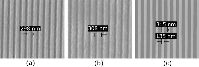
6 Throughout the course of this work, 45 samples were exposed and developed. Many of these samples resulted in grating structures, but we focused on three in particular (a, b, and c) because in these cases we had measured the spectrum of the laser immediately prior to these exposures. These samples were characterized by optical inspection and microscopy, electron microscopy, and diffraction-efficiency mapping as discussed above. Figure 2 shows SEM images of patterned regions of each of the three samples (a,b,c), and corresponding measurements of the grating periods. SEM images confirmed qualitative evaluation of the gratings: grating (a) and (c) exhibited superior diffraction quality upon visual inspection under normal ambient room illumination, while grating (b) required inspection in bright light (ideally full sunlight). Furthermore, they provided a precise measurement of the grating period (298 nm, 308 nm, and 315 nm for gratings (a), (b), and (c) respectively). We hypothesize that the observed variance of a few percent in grating period was due to variation in alignment of the laser and machinist's block from run to run. Assuming that the variance in grating period was due to a corresponding variance in the angle of incidence of the laser on the substrate, we determined this angle by using the SEMmeasured grating periods. The period p i can be related to the half-angle of the interfering beams θ i (which can vary slightly depending on the configuration of the machinist's block or alignment of the laser) by the formula: λi pi (1) 2sin θ i where i is the corresponding sample index, a, b, or c, and λ i is the wavelength at the peak of the optical spectrum. The measured period for each sample and average wavelength for that exposure was used in conjunction with equation 1 to establish the half-angle between the two 6
7 interfering beams. For p a = 298 nm, p b = 308 nm and p c = 315 nm, and λ a = λ b = nm and λ c = nm (the peaks of the measured laser spectra in each case), the angle corresponds to θ a = 43.3, θ b = 41.6 and θ c = The observed variance of a few degrees is consistent with the care taken in alignment of each sample (which was performed by eye). As discussed earlier, diffraction efficiency (and pattern quality) varied greatly across samples on the length scale of millimeters. We hypothesize that this variance was associated with the imperfect temporal coherence of the source. To support this hypothesis, we compared the measured spatial distribution of diffraction efficiency to the calculated fringe contrast based on the measured source spectrum. The fringe contrast can be calculated (by using the measured source spectrum and the relationship given by equation 1) as a function of grating position by using the equation: 0 2 L i c V L I e d (2) where L is the optical path difference between the two arms of the interferometer [7]. The optical path difference can be related to the distance x from the intersection of the mirror with the sample surface by using the equation x L sin θ 1 cos π 2θ. (3) Figure 3 shows the impact of the laser spectrum on the diffraction efficiency of the final grating: the spectrum was measured, used to calculate the fringe visibility distribution, and then compared to the measured diffraction efficiency. Figure 3a shows the measured laser spectrum prior to exposing the sample shown in fig. 2a. Figure 3b shows a calculation of the expected fringe visibility vs. position on the substrate, calculated using the laser optical spectrum shown in 7
8 fig. 3a. Finally, fig. 3c shows the measured diffraction efficiency. Notice the recurrence of regions with strong diffraction visibility observed, and predicted from the calculated result in fig. 3b. We interpret this recurrence as being due to the beating of distinct power peaks in the optical spectrum. 4. Discussion and Summary Inexpensive 405nm diode lasers do have some limitations that need to be addressed in order to improve the system performance. Generally, they are multi-mode, and as a result exhibit poor spatial and temporal coherence. Also, the output power from these inexpensive 405 nm laser diodes is not controlled via feedback with a photodiode [8]. These limitations will restrict the extent and stability of an interference pattern; however, despite these challenges the use of 405 nm diode laser sources can still be of practical use for IL. The key to realizing cm 2 or larger patterning areas in future work is primarily improving the coherence length of the source. This can be simply accomplished either by purchasing singlemode sources (which currently are available for ~ 2000 USD), or by suppressing additional modes by using optical feedback from an external cavity. These approaches will be the subject of future work. To this point, we have focused on construction and utilization of the IL tool and have not described the design of the substrate resist system that would be most suitable for process development. While simple designs are preferred, the ideal photoresist structure for process development is a dense pattern that has a resist lines with rectangular cross-section. This type of profile can be achieved in resist when the thickness of the interlayers between the substrate and resist are chosen appropriately to reduce undesired optical interference in the resist. This interference arises from reflections of the incident light as it crosses the material interfaces 8
9 beneath the photoresist. These reflections are collectively referred to as the back reflectance into the photoresist. If the back reflectance is not suppressed [6], it will cause an additional standingwave to develop in the vertical walls of the grating. After development, this standing-wave can then be transferred during subsequent processing steps, so reducing its amplitude is important. Fortunately, algorithms exist [9] that can be used to design the thickness of an ARC layer to reduce these back reflections. Using one of these, an ARC thickness (~200 nm for our setup) can be chosen to reduce the back reflectance to as low as 1% or 2%. The key result of this paper was the demonstration of ~ 300 nm-pitch patterning capability at low cost. For less than 1000 USD, we were able to print grating lines with our Lloyd s mirror. The capabilities and accessibility of this tool suggest that 405 nm diode lasers could be used as sources for IL in both laboratory and educational settings. 5. Acknowledgements The authors would like to acknowledge Tim Savas and Thomas O Reilly for their helpful discussions about the diffraction grating artifacts, Jeremy Johnson for his help in measuring the optical spectrums and Maria Csete for her help in setting the polarization of the interferometer. Funding for this project was provided by the Singapore-MIT Alliance 6. References [1] M. Walsh, On the design of lithographic interferometers and their application, Ph.D Thesis, MIT, 2004, DSpace.mit.edu. [2] A. Kouchiyama, K. Aratani, Y. Takemoto, T.Nakao, S. Kai, K. Osato and K. Nakagawa, Jpn. J. Appl. Phys. 42, (2003). [3] Heidelburg Instruments, (downloaded June 16, 2009). [4] C. C. Su, T. C. Wu, J. H. Hsu, S. J. Hwang and S. H. Chang, in Proceedings of the 34th Micro and Nano Engineering Conference, Greece,
10 [5] David Tanenbaum, personal communication We ve recently become aware that other groups are using 405 nm diode lasers as sources for IL. [6] M. L. Schattenburg, R. J. Aucoin and R. C. Fleming, J. Vac. Sci. Technol. B 13, 6, (1995). [7] J. Goodman, Statistical Optics, Wiley classics library ed. (Wiley, New York, NY, USA, 2000), pp [8] C. E. Wieman, L. Hollberg, Rev. Sci. Instrum. 62, 1, 1-20 (1991). [9] M. G. Moharam, D. A. Pommet, E. B. Grann and T. K. Gaylord, J. Opt. Soc. America 12, 5, (1995). 10
11 Figure 1: Two configurations of the Lloyd's mirror lithography system: (a) includes a collimated, long coherence length source and spatial filter upstream of the mirror/substrate chuck to improve the beam quality; and (b) includes both an inexpensive 405 nm diode laser and an inexpensive mirror/substrate chuck. In (a), the mirror/substrate chuck holds both a mirror and substrate in a perpendicular orientation, which can be rotated to control the pattern pitch. In (b), the same configuration is chosen but the chuck is fixed, the spatial filter is removed and the gas laser is replaced by a 405-nm diode laser. Figure 2: Three exposures with different doses and spectra, taken on three different days, separated by several weeks. Note, the incident angles, θ a, θ b, θ c, in the three images varied slightly from run to run, but could be calculated from the period of the gratings shown in (a), (b), and (c). The associated periods and the known wavelengths for each sample can then be used to determine the angle of incidence of the laser on the surface. Figure 3: (a) Laser spectrum, measured before the exposure for the sample shown in figure 2a. (b) Calculated fringe visibility projected onto the wafer surface. The incident angle during the exposure was calculated from equation 1 and used to project the fringe visibility onto the surface of the substrate through equation 3. (c) Measured 1 st order diffracted power from the grating. The first order diffracted power was normalized over the interval from 0 to 1. 11
12
Project Staff: Timothy A. Savas, Michael E. Walsh, Thomas B. O'Reilly, Dr. Mark L. Schattenburg, and Professor Henry I. Smith
 9. Interference Lithography Sponsors: National Science Foundation, DMR-0210321; Dupont Agreement 12/10/99 Project Staff: Timothy A. Savas, Michael E. Walsh, Thomas B. O'Reilly, Dr. Mark L. Schattenburg,
Lithography. 3 rd. lecture: introduction. Prof. Yosi Shacham-Diamand. Fall 2004
 Lithography 3 rd lecture: introduction Prof. Yosi Shacham-Diamand Fall 2004 1 List of content Fundamental principles Characteristics parameters Exposure systems 2 Fundamental principles Aerial Image Exposure
Major Fabrication Steps in MOS Process Flow
 Major Fabrication Steps in MOS Process Flow UV light Mask oxygen Silicon dioxide photoresist exposed photoresist oxide Silicon substrate Oxidation (Field oxide) Photoresist Coating Mask-Wafer Alignment
CHAPTER 5 FINE-TUNING OF AN ECDL WITH AN INTRACAVITY LIQUID CRYSTAL ELEMENT
 CHAPTER 5 FINE-TUNING OF AN ECDL WITH AN INTRACAVITY LIQUID CRYSTAL ELEMENT In this chapter, the experimental results for fine-tuning of the laser wavelength with an intracavity liquid crystal element
Synthesis of projection lithography for low k1 via interferometry
 Synthesis of projection lithography for low k1 via interferometry Frank Cropanese *, Anatoly Bourov, Yongfa Fan, Andrew Estroff, Lena Zavyalova, Bruce W. Smith Center for Nanolithography Research, Rochester
Laser Telemetric System (Metrology)
") Laser Telemetric System (Metrology) Laser telemetric system is a non-contact gauge that measures with a collimated laser beam (Refer Fig. 10.26). It measure at the rate of 150 scans per second. It basically
Laser Telemetric System (Metrology) Laser telemetric system is a non-contact gauge that measures with a collimated laser beam (Refer Fig. 10.26). It measure at the rate of 150 scans per second. It basically
Simple interferometric fringe stabilization by CCD-based feedback control
 Simple interferometric fringe stabilization by CCD-based feedback control Preston P. Young and Purnomo S. Priambodo, Department of Electrical Engineering, University of Texas at Arlington, P.O. Box 19016,
Doppler writing and linewidth control for scanning beam interference lithography
 Doppler writing and linewidth control for scanning beam interference lithography Juan C. Montoya, a Chih-Hao Chang, Ralf K. Heilmann, and Mark L. Schattenburg Space Nanotechnology Laboratory, Massachusetts
2.1 BASIC THEORY: INTERFERENCE OF TWO BEAMS
 2 LASER INTERFERENCE LITHOGRAPHY (LIL) 9 2 LASER INTERFERENCE LITHOGRAPHY (LIL) Laser interference lithography [3~22] (LIL) is a method to produce periodic structures using two interfering highly-coherent
Will contain image distance after raytrace Will contain image height after raytrace
 Name: LASR 51 Final Exam May 29, 2002 Answer all questions. Module numbers are for guidance, some material is from class handouts. Exam ends at 8:20 pm. Ynu Raytracing The first questions refer to the
Photolithography II ( Part 2 )
") 1 Photolithography II ( Part 2 ) Chapter 14 : Semiconductor Manufacturing Technology by M. Quirk & J. Serda Saroj Kumar Patra, Department of Electronics and Telecommunication, Norwegian University of Science
1 Photolithography II ( Part 2 ) Chapter 14 : Semiconductor Manufacturing Technology by M. Quirk & J. Serda Saroj Kumar Patra, Department of Electronics and Telecommunication, Norwegian University of Science
Sub-50 nm period patterns with EUV interference lithography
 Microelectronic Engineering 67 68 (2003) 56 62 www.elsevier.com/ locate/ mee Sub-50 nm period patterns with EUV interference lithography * a, a a b b b H.H. Solak, C. David, J. Gobrecht, V. Golovkina,
Micro- and Nano-Technology... for Optics
 Micro- and Nano-Technology...... for Optics 3.2 Lithography U.D. Zeitner Fraunhofer Institut für Angewandte Optik und Feinmechanik Jena Printing on Stones Map of Munich Stone Print Contact Printing light
A novel tunable diode laser using volume holographic gratings
 A novel tunable diode laser using volume holographic gratings Christophe Moser *, Lawrence Ho and Frank Havermeyer Ondax, Inc. 85 E. Duarte Road, Monrovia, CA 9116, USA ABSTRACT We have developed a self-aligned
Project Staff: Feng Zhang, Prof. Jianfeng Dai (Lanzhou Univ. of Tech.), Prof. Todd Hasting (Univ. Kentucky), Prof. Henry I. Smith
, Prof. Todd Hasting (Univ. Kentucky), Prof. Henry I. Smith") 3. Spatial-Phase-Locked Electron-Beam Lithography Sponsors: No external sponsor Project Staff: Feng Zhang, Prof. Jianfeng Dai (Lanzhou Univ. of Tech.), Prof. Todd Hasting (Univ. Kentucky), Prof. Henry
3. Spatial-Phase-Locked Electron-Beam Lithography Sponsors: No external sponsor Project Staff: Feng Zhang, Prof. Jianfeng Dai (Lanzhou Univ. of Tech.), Prof. Todd Hasting (Univ. Kentucky), Prof. Henry
Exercise 8: Interference and diffraction
 Physics 223 Name: Exercise 8: Interference and diffraction 1. In a two-slit Young s interference experiment, the aperture (the mask with the two slits) to screen distance is 2.0 m, and a red light of wavelength
Development of a new multi-wavelength confocal surface profilometer for in-situ automatic optical inspection (AOI)
") Development of a new multi-wavelength confocal surface profilometer for in-situ automatic optical inspection (AOI) Liang-Chia Chen 1#, Chao-Nan Chen 1 and Yi-Wei Chang 1 1. Institute of Automation Technology,
Development of a new multi-wavelength confocal surface profilometer for in-situ automatic optical inspection (AOI) Liang-Chia Chen 1#, Chao-Nan Chen 1 and Yi-Wei Chang 1 1. Institute of Automation Technology,
Infrared broadband 50%-50% beam splitters for s- polarized light
 University of New Orleans ScholarWorks@UNO Electrical Engineering Faculty Publications Department of Electrical Engineering 7-1-2006 Infrared broadband 50%-50% beam splitters for s- polarized light R.
plasmonic nanoblock pair
 Nanostructured potential of optical trapping using a plasmonic nanoblock pair Yoshito Tanaka, Shogo Kaneda and Keiji Sasaki* Research Institute for Electronic Science, Hokkaido University, Sapporo 1-2,
Large-Area Interference Lithography Exposure Tool Development
 Large-Area Interference Lithography Exposure Tool Development John Burnett 1, Eric Benck 1 and James Jacob 2 1 Physical Measurements Laboratory, NIST, Gaithersburg, MD, USA 2 Actinix, Scotts Valley, CA
EG2605 Undergraduate Research Opportunities Program. Large Scale Nano Fabrication via Proton Lithography Using Metallic Stencils
 EG2605 Undergraduate Research Opportunities Program Large Scale Nano Fabrication via Proton Lithography Using Metallic Stencils Tan Chuan Fu 1, Jeroen Anton van Kan 2, Pattabiraman Santhana Raman 2, Yao
Lab 12 Microwave Optics.
 b Lab 12 Microwave Optics. CAUTION: The output power of the microwave transmitter is well below standard safety levels. Nevertheless, do not look directly into the microwave horn at close range when the
MASSACHUSETTS INSTITUTE OF TECHNOLOGY Department of Electrical Engineering and Computer Science
 Student Name Date MASSACHUSETTS INSTITUTE OF TECHNOLOGY Department of Electrical Engineering and Computer Science 6.161 Modern Optics Project Laboratory Laboratory Exercise No. 3 Fall 2005 Diffraction
Part 5-1: Lithography
 Part 5-1: Lithography Yao-Joe Yang 1 Pattern Transfer (Patterning) Types of lithography systems: Optical X-ray electron beam writer (non-traditional, no masks) Two-dimensional pattern transfer: limited
2. Pulsed Acoustic Microscopy and Picosecond Ultrasonics
 1st International Symposium on Laser Ultrasonics: Science, Technology and Applications July 16-18 2008, Montreal, Canada Picosecond Ultrasonic Microscopy of Semiconductor Nanostructures Thomas J GRIMSLEY
Waveguiding in PMMA photonic crystals
 ROMANIAN JOURNAL OF INFORMATION SCIENCE AND TECHNOLOGY Volume 12, Number 3, 2009, 308 316 Waveguiding in PMMA photonic crystals Daniela DRAGOMAN 1, Adrian DINESCU 2, Raluca MÜLLER2, Cristian KUSKO 2, Alex.
Section 2: Lithography. Jaeger Chapter 2. EE143 Ali Javey Slide 5-1
 Section 2: Lithography Jaeger Chapter 2 EE143 Ali Javey Slide 5-1 The lithographic process EE143 Ali Javey Slide 5-2 Photolithographic Process (a) (b) (c) (d) (e) (f) (g) Substrate covered with silicon
PHY 431 Homework Set #5 Due Nov. 20 at the start of class
 PHY 431 Homework Set #5 Due Nov. 0 at the start of class 1) Newton s rings (10%) The radius of curvature of the convex surface of a plano-convex lens is 30 cm. The lens is placed with its convex side down
PhysicsAndMathsTutor.com 1
 PhysicsAndMathsTutor.com 1 Q1. Just over two hundred years ago Thomas Young demonstrated the interference of light by illuminating two closely spaced narrow slits with light from a single light source.
Fabrication of large grating by monitoring the latent fringe pattern
 Fabrication of large grating by monitoring the latent fringe pattern Lijiang Zeng a, Lei Shi b, and Lifeng Li c State Key Laboratory of Precision Measurement Technology and Instruments Department of Precision
Integrated into Nanowire Waveguides
 Supporting Information Widely Tunable Distributed Bragg Reflectors Integrated into Nanowire Waveguides Anthony Fu, 1,3 Hanwei Gao, 1,3,4 Petar Petrov, 1, Peidong Yang 1,2,3* 1 Department of Chemistry,
Holography as a tool for advanced learning of optics and photonics
 Holography as a tool for advanced learning of optics and photonics Victor V. Dyomin, Igor G. Polovtsev, Alexey S. Olshukov Tomsk State University 36 Lenin Avenue, Tomsk, 634050, Russia Tel/fax: 7 3822
Supplementary Figure 1 Reflective and refractive behaviors of light with normal
 Supplementary Figures Supplementary Figure 1 Reflective and refractive behaviors of light with normal incidence in a three layer system. E 1 and E r are the complex amplitudes of the incident wave and
Photolithography Technology and Application
 Photolithography Technology and Application Jeff Tsai Director, Graduate Institute of Electro-Optical Engineering Tatung University Art or Science? Lind width = 100 to 5 micron meter!! Resolution = ~ 3
Diffraction. Interference with more than 2 beams. Diffraction gratings. Diffraction by an aperture. Diffraction of a laser beam
 Diffraction Interference with more than 2 beams 3, 4, 5 beams Large number of beams Diffraction gratings Equation Uses Diffraction by an aperture Huygen s principle again, Fresnel zones, Arago s spot Qualitative
Test procedures Page: 1 of 5
 Test procedures Page: 1 of 5 1 Scope This part of document establishes uniform requirements for measuring the numerical aperture of optical fibre, thereby assisting in the inspection of fibres and cables
Spectroscopy Lab 2. Reading Your text books. Look under spectra, spectrometer, diffraction.
 1 Spectroscopy Lab 2 Reading Your text books. Look under spectra, spectrometer, diffraction. Consult Sargent Welch Spectrum Charts on wall of lab. Note that only the most prominent wavelengths are displayed
Polarization Experiments Using Jones Calculus
 Polarization Experiments Using Jones Calculus Reference http://chaos.swarthmore.edu/courses/physics50_2008/p50_optics/04_polariz_matrices.pdf Theory In Jones calculus, the polarization state of light is
UV LED ILLUMINATION STEPPER OFFERS HIGH PERFORMANCE AND LOW COST OF OWNERSHIP
 UV LED ILLUMINATION STEPPER OFFERS HIGH PERFORMANCE AND LOW COST OF OWNERSHIP Casey Donaher, Rudolph Technologies Herbert J. Thompson, Rudolph Technologies Chin Tiong Sim, Rudolph Technologies Rudolph
EUV Interference Lithography in NewSUBARU
 EUV Interference Lithography in NewSUBARU Takeo Watanabe 1, Tae Geun Kim 2, Yasuyuki Fukushima 1, Noki Sakagami 1, Teruhiko Kimura 1, Yoshito Kamaji 1, Takafumi Iguchi 1, Yuuya Yamaguchi 1, Masaki Tada
Planar micro-optic solar concentration. Jason H. Karp
 Planar micro-optic solar concentration Jason H. Karp Eric J. Tremblay, Katherine A. Baker and Joseph E. Ford Photonics Systems Integration Lab University of California San Diego Jacobs School of Engineering
LOS 1 LASER OPTICS SET
 LOS 1 LASER OPTICS SET Contents 1 Introduction 3 2 Light interference 5 2.1 Light interference on a thin glass plate 6 2.2 Michelson s interferometer 7 3 Light diffraction 13 3.1 Light diffraction on a
FINDINGS. REU Student: Philip Garcia Graduate Student Mentor: Anabil Chaudhuri Faculty Mentor: Steven R. J. Brueck. Figure 1
 FINDINGS REU Student: Philip Garcia Graduate Student Mentor: Anabil Chaudhuri Faculty Mentor: Steven R. J. Brueck A. Results At the Center for High Tech Materials at the University of New Mexico, my work
Imaging Systems Laboratory II. Laboratory 8: The Michelson Interferometer / Diffraction April 30 & May 02, 2002
 1051-232 Imaging Systems Laboratory II Laboratory 8: The Michelson Interferometer / Diffraction April 30 & May 02, 2002 Abstract. In the last lab, you saw that coherent light from two different locations
Single Slit Diffraction
 PC1142 Physics II Single Slit Diffraction 1 Objectives Investigate the single-slit diffraction pattern produced by monochromatic laser light. Determine the wavelength of the laser light from measurements
DOE Project: Resist Characterization
 DOE Project: Resist Characterization GOAL To achieve high resolution and adequate throughput, a photoresist must possess relatively high contrast and sensitivity to exposing radiation. The objective of
Supporting Information
 Electronic Supplementary Material (ESI) for Materials Horizons. This journal is The Royal Society of Chemistry 2017 Supporting Information Nanofocusing of circularly polarized Bessel-type plasmon polaritons
Linewidth control by overexposure in laser lithography
 Optica Applicata, Vol. XXXVIII, No. 2, 2008 Linewidth control by overexposure in laser lithography LIANG YIYONG*, YANG GUOGUANG State Key Laboratory of Modern Optical Instruments, Zhejiang University,
MICRO AND NANOPROCESSING TECHNOLOGIES
 MICRO AND NANOPROCESSING TECHNOLOGIES LECTURE 4 Optical lithography Concepts and processes Lithography systems Fundamental limitations and other issues Photoresists Photolithography process Process parameter
LASER INTERFERENCE LITHOGRAPHY
 In: Lithography: Principles, Processes and Materials ISBN: 978-1-61761-837-6 Editor: Theodore C. Hennessy, pp. 133-148 2011 Nova Science Publishers, Inc. The exclusive license for this PDF is limited to
TriVista. Universal Raman Solution
 TriVista Universal Raman Solution Why choose the Princeton Instruments/Acton TriVista? Overview Raman Spectroscopy systems can be derived from several dispersive components depending on the level of performance
Lab Report 3: Speckle Interferometry LIN PEI-YING, BAIG JOVERIA
 Lab Report 3: Speckle Interferometry LIN PEI-YING, BAIG JOVERIA Abstract: Speckle interferometry (SI) has become a complete technique over the past couple of years and is widely used in many branches of
Supplementary Figure 1. Effect of the spacer thickness on the resonance properties of the gold and silver metasurface layers.
 Supplementary Figure 1. Effect of the spacer thickness on the resonance properties of the gold and silver metasurface layers. Finite-difference time-domain calculations of the optical transmittance through
PHYS General Physics II Lab Diffraction Grating
 1 PHYS 1040 - General Physics II Lab Diffraction Grating In this lab you will perform an experiment to understand the interference of light waves when they pass through a diffraction grating and to determine
Section 2: Lithography. Jaeger Chapter 2 Litho Reader. The lithographic process
 Section 2: Lithography Jaeger Chapter 2 Litho Reader The lithographic process Photolithographic Process (a) (b) (c) (d) (e) (f) (g) Substrate covered with silicon dioxide barrier layer Positive photoresist
Fabrication of Probes for High Resolution Optical Microscopy
 Fabrication of Probes for High Resolution Optical Microscopy Physics 564 Applied Optics Professor Andrès La Rosa David Logan May 27, 2010 Abstract Near Field Scanning Optical Microscopy (NSOM) is a technique
MASSACHUSETTS INSTITUTE OF TECHNOLOGY Department of Electrical Engineering and Computer Science
 Student Name Date MASSACHUSETTS INSTITUTE OF TECHNOLOGY Department of Electrical Engineering and Computer Science 6.161 Modern Optics Project Laboratory Laboratory Exercise No. 6 Fall 2010 Solid-State
LOPUT Laser: A novel concept to realize single longitudinal mode laser
 PRAMANA c Indian Academy of Sciences Vol. 82, No. 2 journal of February 2014 physics pp. 185 190 LOPUT Laser: A novel concept to realize single longitudinal mode laser JGEORGE, KSBINDRAand SMOAK Solid
Section 2: Lithography. Jaeger Chapter 2 Litho Reader. EE143 Ali Javey Slide 5-1
 Section 2: Lithography Jaeger Chapter 2 Litho Reader EE143 Ali Javey Slide 5-1 The lithographic process EE143 Ali Javey Slide 5-2 Photolithographic Process (a) (b) (c) (d) (e) (f) (g) Substrate covered
Observational Astronomy
 Observational Astronomy Instruments The telescope- instruments combination forms a tightly coupled system: Telescope = collecting photons and forming an image Instruments = registering and analyzing the
EE-527: MicroFabrication
 EE-57: MicroFabrication Exposure and Imaging Photons white light Hg arc lamp filtered Hg arc lamp excimer laser x-rays from synchrotron Electrons Ions Exposure Sources focused electron beam direct write
Microlens formation using heavily dyed photoresist in a single step
 Microlens formation using heavily dyed photoresist in a single step Chris Cox, Curtis Planje, Nick Brakensiek, Zhimin Zhu, Jonathan Mayo Brewer Science, Inc., 2401 Brewer Drive, Rolla, MO 65401, USA ABSTRACT
Supplementary Materials
 Supplementary Materials In the supplementary materials of this paper we discuss some practical consideration for alignment of optical components to help unexperienced users to achieve a high performance
A process for, and optical performance of, a low cost Wire Grid Polarizer
 1.0 Introduction A process for, and optical performance of, a low cost Wire Grid Polarizer M.P.C.Watts, M. Little, E. Egan, A. Hochbaum, Chad Jones, S. Stephansen Agoura Technology Low angle shadowed deposition
Chapter 3 Fabrication
 Chapter 3 Fabrication The total structure of MO pick-up contains four parts: 1. A sub-micro aperture underneath the SIL The sub-micro aperture is used to limit the final spot size from 300nm to 600nm for
IST IP NOBEL "Next generation Optical network for Broadband European Leadership"
 DBR Tunable Lasers A variation of the DFB laser is the distributed Bragg reflector (DBR) laser. It operates in a similar manner except that the grating, instead of being etched into the gain medium, is
The End of Thresholds: Subwavelength Optical Linewidth Measurement Using the Flux-Area Technique
 The End of Thresholds: Subwavelength Optical Linewidth Measurement Using the Flux-Area Technique Peter Fiekowsky Automated Visual Inspection, Los Altos, California ABSTRACT The patented Flux-Area technique
Photolithography I ( Part 1 )
") 1 Photolithography I ( Part 1 ) Chapter 13 : Semiconductor Manufacturing Technology by M. Quirk & J. Serda Bjørn-Ove Fimland, Department of Electronics and Telecommunication, Norwegian University of Science
1 Photolithography I ( Part 1 ) Chapter 13 : Semiconductor Manufacturing Technology by M. Quirk & J. Serda Bjørn-Ove Fimland, Department of Electronics and Telecommunication, Norwegian University of Science
Development of innovative fringe locking strategies for vibration-resistant white light vertical scanning interferometry (VSI)
") Development of innovative fringe locking strategies for vibration-resistant white light vertical scanning interferometry (VSI) Liang-Chia Chen 1), Abraham Mario Tapilouw 1), Sheng-Lih Yeh 2), Shih-Tsong
Development of innovative fringe locking strategies for vibration-resistant white light vertical scanning interferometry (VSI) Liang-Chia Chen 1), Abraham Mario Tapilouw 1), Sheng-Lih Yeh 2), Shih-Tsong
Physics 3340 Spring 2005
 Physics 3340 Spring 2005 Holography Purpose The goal of this experiment is to learn the basics of holography by making a two-beam transmission hologram. Introduction A conventional photograph registers
Applications of Maskless Lithography for the Production of Large Area Substrates Using the SF-100 ELITE. Jay Sasserath, PhD
 Applications of Maskless Lithography for the Production of Large Area Substrates Using the SF-100 ELITE Executive Summary Jay Sasserath, PhD Intelligent Micro Patterning LLC St. Petersburg, Florida Processing
GRENOUILLE.
 GRENOUILLE Measuring ultrashort laser pulses the shortest events ever created has always been a challenge. For many years, it was possible to create ultrashort pulses, but not to measure them. Techniques
Micro-Optic Solar Concentration and Next-Generation Prototypes
 Micro-Optic Solar Concentration and Next-Generation Prototypes Jason H. Karp, Eric J. Tremblay and Joseph E. Ford Photonics Systems Integration Lab University of California San Diego Jacobs School of Engineering
Fabrication Methodology of microlenses for stereoscopic imagers using standard CMOS process. R. P. Rocha, J. P. Carmo, and J. H.
 Fabrication Methodology of microlenses for stereoscopic imagers using standard CMOS process R. P. Rocha, J. P. Carmo, and J. H. Correia Department of Industrial Electronics, University of Minho, Campus
R. J. Jones College of Optical Sciences OPTI 511L Fall 2017
 R. J. Jones College of Optical Sciences OPTI 511L Fall 2017 Active Modelocking of a Helium-Neon Laser The generation of short optical pulses is important for a wide variety of applications, from time-resolved
Introduction to the operating principles of the HyperFine spectrometer
 Introduction to the operating principles of the HyperFine spectrometer LightMachinery Inc., 80 Colonnade Road North, Ottawa ON Canada A spectrometer is an optical instrument designed to split light into
Low aberration monolithic diffraction gratings for high performance optical spectrometers
 Low aberration monolithic diffraction gratings for high performance optical spectrometers Peter Triebel, Tobias Moeller, Torsten Diehl; Carl Zeiss Spectroscopy GmbH (Germany) Alexandre Gatto, Alexander
A Laser-Based Thin-Film Growth Monitor
 TECHNOLOGY by Charles Taylor, Darryl Barlett, Eric Chason, and Jerry Floro A Laser-Based Thin-Film Growth Monitor The Multi-beam Optical Sensor (MOS) was developed jointly by k-space Associates (Ann Arbor,
EE143 Fall 2016 Microfabrication Technologies. Lecture 3: Lithography Reading: Jaeger, Chap. 2
 EE143 Fall 2016 Microfabrication Technologies Lecture 3: Lithography Reading: Jaeger, Chap. 2 Prof. Ming C. Wu wu@eecs.berkeley.edu 511 Sutardja Dai Hall (SDH) 1-1 The lithographic process 1-2 1 Photolithographic
A Narrow-Band Tunable Diode Laser System with Grating Feedback
 A Narrow-Band Tunable Diode Laser System with Grating Feedback S.P. Spirydovich Draft Abstract The description of diode laser was presented. The tuning laser system was built and aligned. The free run
Laser Speckle Reducer LSR-3000 Series
 Datasheet: LSR-3000 Series Update: 06.08.2012 Copyright 2012 Optotune Laser Speckle Reducer LSR-3000 Series Speckle noise from a laser-based system is reduced by dynamically diffusing the laser beam. A
Application Note #548 AcuityXR Technology Significantly Enhances Lateral Resolution of White-Light Optical Profilers
 Application Note #548 AcuityXR Technology Significantly Enhances Lateral Resolution of White-Light Optical Profilers ContourGT with AcuityXR TM capability White light interferometry is firmly established
Infrared wire grid polarizers: metrology, modeling, and laser damage threshold
 Infrared wire grid polarizers: metrology, modeling, and laser damage threshold Matthew George, Bin Wang, Jonathon Bergquist, Rumyana Petrova, Eric Gardner Moxtek Inc. Calcon 2013 Wire Grid Polarizer (WGP)
attosnom I: Topography and Force Images NANOSCOPY APPLICATION NOTE M06 RELATED PRODUCTS G
 APPLICATION NOTE M06 attosnom I: Topography and Force Images Scanning near-field optical microscopy is the outstanding technique to simultaneously measure the topography and the optical contrast of a sample.
Radial Coupling Method for Orthogonal Concentration within Planar Micro-Optic Solar Collectors
 Radial Coupling Method for Orthogonal Concentration within Planar Micro-Optic Solar Collectors Jason H. Karp, Eric J. Tremblay and Joseph E. Ford Photonics Systems Integration Lab University of California
Outline. 1 Introduction. 2 Basic IC fabrication processes. 3 Fabrication techniques for MEMS. 4 Applications. 5 Mechanics issues on MEMS MDL NTHU
 Outline 1 Introduction 2 Basic IC fabrication processes 3 Fabrication techniques for MEMS 4 Applications 5 Mechanics issues on MEMS 2.2 Lithography Reading: Runyan Chap. 5, or 莊達人 Chap. 7, or Wolf and
attocfm I for Surface Quality Inspection NANOSCOPY APPLICATION NOTE M01 RELATED PRODUCTS G
 APPLICATION NOTE M01 attocfm I for Surface Quality Inspection Confocal microscopes work by scanning a tiny light spot on a sample and by measuring the scattered light in the illuminated volume. First,
Design and Analysis of Resonant Leaky-mode Broadband Reflectors
 846 PIERS Proceedings, Cambridge, USA, July 6, 8 Design and Analysis of Resonant Leaky-mode Broadband Reflectors M. Shokooh-Saremi and R. Magnusson Department of Electrical and Computer Engineering, University
immersion optics Immersion Lithography with ASML HydroLith TWINSCAN System Modifications for Immersion Lithography by Bob Streefkerk
 immersion optics Immersion Lithography with ASML HydroLith by Bob Streefkerk For more than 25 years, many in the semiconductor industry have predicted the end of optical lithography. Recent developments,
Characteristics of point-focus Simultaneous Spatial and temporal Focusing (SSTF) as a two-photon excited fluorescence microscopy
 as a two-photon excited fluorescence microscopy") Characteristics of point-focus Simultaneous Spatial and temporal Focusing (SSTF) as a two-photon excited fluorescence microscopy Qiyuan Song (M2) and Aoi Nakamura (B4) Abstracts: We theoretically and experimentally
Characteristics of point-focus Simultaneous Spatial and temporal Focusing (SSTF) as a two-photon excited fluorescence microscopy Qiyuan Song (M2) and Aoi Nakamura (B4) Abstracts: We theoretically and experimentally
Radial Polarization Converter With LC Driver USER MANUAL
 ARCoptix Radial Polarization Converter With LC Driver USER MANUAL Arcoptix S.A Ch. Trois-portes 18 2000 Neuchâtel Switzerland Mail: info@arcoptix.com Tel: ++41 32 731 04 66 Principle of the radial polarization
Sensitive measurement of partial coherence using a pinhole array
 1.3 Sensitive measurement of partial coherence using a pinhole array Paul Petruck 1, Rainer Riesenberg 1, Richard Kowarschik 2 1 Institute of Photonic Technology, Albert-Einstein-Strasse 9, 07747 Jena,
PREPARED BY: I. Miller DATE: 2004 May 23 CO-OWNERS REVISED DATE OF ISSUE/CHANGED PAGES
 Page 1 of 30 LIGHTMACHINERY TEST REPORT LQT 30.11-1 TITLE: HMI Michelson Interferometer Test Report Serial Number 1 - Wideband FSR INSTRUCTION OWNER HMI Project Manager PREPARED BY: I. Miller DATE: 2004
Integrated Focusing Photoresist Microlenses on AlGaAs Top-Emitting VCSELs
 Integrated Focusing Photoresist Microlenses on AlGaAs Top-Emitting VCSELs Andrea Kroner We present 85 nm wavelength top-emitting vertical-cavity surface-emitting lasers (VCSELs) with integrated photoresist
Diffraction, Fourier Optics and Imaging
 1 Diffraction, Fourier Optics and Imaging 1.1 INTRODUCTION When wave fields pass through obstacles, their behavior cannot be simply described in terms of rays. For example, when a plane wave passes through
Silicon Photonic Device Based on Bragg Grating Waveguide
 Silicon Photonic Device Based on Bragg Grating Waveguide Hwee-Gee Teo, 1 Ming-Bin Yu, 1 Guo-Qiang Lo, 1 Kazuhiro Goi, 2 Ken Sakuma, 2 Kensuke Ogawa, 2 Ning Guan, 2 and Yong-Tsong Tan 2 Silicon photonics
7. Michelson Interferometer
 7. Michelson Interferometer In this lab we are going to observe the interference patterns produced by two spherical waves as well as by two plane waves. We will study the operation of a Michelson interferometer,
i- Line Photoresist Development: Replacement Evaluation of OiR
 i- Line Photoresist Development: Replacement Evaluation of OiR 906-12 Nishtha Bhatia High School Intern 31 July 2014 The Marvell Nanofabrication Laboratory s current i-line photoresist, OiR 897-10i, has
Characterization of field stitching in electron-beam lithography using moiré metrology
 Characterization of field stitching in electron-beam lithography using moiré metrology T. E. Murphy, a) Mark K. Mondol, and Henry I. Smith Massachusetts Institute of Technology, 60 Vassar Street, Cambridge,
ECEN. Spectroscopy. Lab 8. copy. constituents HOMEWORK PR. Figure. 1. Layout of. of the
 ECEN 4606 Lab 8 Spectroscopy SUMMARY: ROBLEM 1: Pedrotti 3 12-10. In this lab, you will design, build and test an optical spectrum analyzer and use it for both absorption and emission spectroscopy. The