Atomic Scale Patterning Made Easy
|
|
|
- Derick Boyd
- 5 years ago
- Views:
Transcription

1 ZyVector STM Control System for Atomically Precise Lithography Making Atomic Resolution Lithography a reality Distributed by Distortion-Free Imaging Automatic Lattice Alignment Digital Vector Lithography Precise Tip Motion with real-time position correction Automation and Scripting


2 ZyVector Atomic Scale Patterning Made Easy At Zyvex Labs, our vision is to design, construct, and commercialize the world s most precise manufactured products. For nearly 20 years, Zyvex Corp, LLC, has been at the forefront of developing tools and processes to create ultraminiaturized systems with atomic precision and unprecedented capability. Sister companies include Zyvex Technologies, the world s leading supplier of carbon nanotube polymers, and Zyvex Instruments, currently owned by ThermoFisher, which is the world leader in nanoprobe testing of integrated circuits. Zyvex Labs is pursuing research and developing tools for creating quantum computers and other transformational systems that require atomic precision, towards its eventual goal of Atomically Precise Manufacturing. Developed as part of this effort, ZyVector turns the world-class ScientaOmicron VT-STM* into an STM lithography tool, creating the only complete commercial solution for atomic precision lithography. *Adaptions for other STM systems possible. Scanz PC software for interface to user USB 20-bit Digital Control box for real-time control ADC DAC High-voltage amplifier box PIC preamp ScientaOmicron VT-STM Digital Vector Lithography Takes atomic structure of surface into account Sub-nm pixel ( 4 surface atoms) Multiple Beam Widths available No partial exposure or proximity effects Automatic alignment of lattice Built-In Metrology Nondestructive imaging mode available New Patterning can be aligned to old Pattern quality can be checked after writing Size of developed nanostructures traceable back to original pattern, with atomic precision. Automation and Scripting Almost all actions can be automated. Command-line interface for single commands or scripts Script Menu for built-in and user-written scripts Multiple pattern input modes - as geometric shapes, vector lists, black/white bitmaps. Precise Tip Positioning and Motion Real-time creep and hysteresis correction enables atomicprecision motion over limited areas; reduced errors over large distances. Automatic alignment to fiducial marks allows for correction of residual errors. Distortion-free imaging for precise tip location. STM Control System for Atomically Precise Lithography


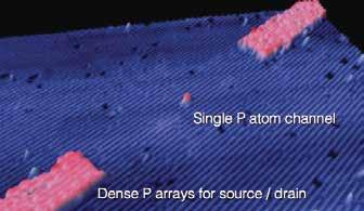


3 Applications Dopant-based Electronics NanoImprint Templates


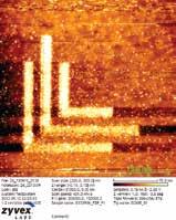
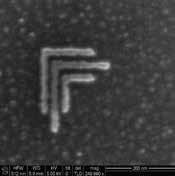
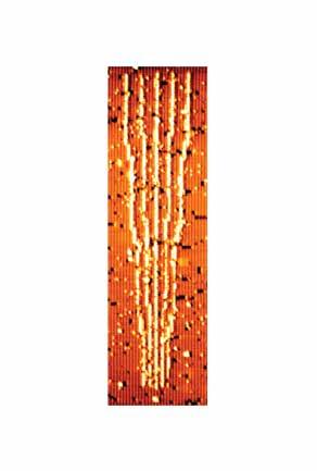
 H -Terminated Dimers Exposed SI Dimers Atomic-scale lithography pixel For the Si(001): H surface, we use a")


4 Digital Vector Lithography Unlike conventional optical or e-beam lithography, STM lithography takes into account the atomic nature of the surface. In ZyVector, writing is done as vectors, moving along the surface lattice directions, rather than a raster scan across the surface as used for STM imaging. Hydrogen Depassivation Lithography (HDL) Lyding et al.* first showed that at a positive sample bias, an STM tip can be used to inject electrons into a surface Si-H bond, until the bond breaks, exposing a chemically reactive Si dangling bond. Other materials are then selectively reacted with the dangling bonds, forming atomically precise nanostructures. *Applied Physics Letters (1994) H -Terminated Dimers Exposed SI Dimers Atomic-scale lithography pixel For the Si(001): H surface, we use a standard pixel size of 2 dimers on a single dimer row, giving a lithography pixel size of nm. Patterns are typically generated from integral numbers of pixels, although for some special cases, such as the 3-dimer pattern used to place single P dopant atoms, half-pixels can be used. Writing to the lattice In order to write atomically-precise patterns, the location of the surface dimer rows are identified from the Fourier Transform of an STM image, and a pixel grid is overlaid onto the image. To perform lithography, the tip is then instructed to move to a particular pixel, change to lithography conditions, and write a line along or across the dimer rows of the desired length. STM Control System for Atomically Precise Lithography


 mode with much wider line widths, but also with rough edges to the lines.")


 is more reliable than simply drawing a very short")
5 Variable Spotsize Lithography STM lithography is digital because it causes the breaking of a Si-H chemical bond by electron excitation. There is no equivalent of partial exposure, because either the bond is broken or it is not. Likewise, there are no proximity effects. Similar to e-beam lithography, with different settings of bias voltage and tunnel current, multiple line widths are available, from 1 px width up to several nm. Under lowvoltage lithography conditions, around +4 V, 4 na, with a dose of 4 mc/cm, the line width of STM lithography is one dimer row. This is known as Atomically Precise or AP mode. Above about 6 V, the tip moves out of tunneling range into Field Emission (FE) mode with much wider line widths, but also with rough edges to the lines. Use of the FE mode is useful to minimize write time for larger patterns, particularly where there is less need for absolute precision. For large patterns which do require precise edges, the modes can even be mixed within a single pattern, writing slowly around the perimeter, and quickly filling in the centre. AP mode: 4.5 V, 4 na, 2 mc/cm 20 nm/s Liinewidth: 1 px 26 px/s FE mode: 8 V, 1 na, 0.1 mc/cm 100 nm/s Linewidth: 4 px 520 px/s Writing Simple Patterns Simple shapes can be selected in the Litho tab and written with just one or two clicks. In the Script Menu tab, geometric patterns can also be called, with editable parameters, such as dimensions and angles. Here, alignment to the lattice can be turned on and off as required. Current, voltage and electron dose parameters are selected in the Litho tab. Preset groups of parameters giving different linewidths can be saved, and quickly selected. Removing single atoms For removal of single H atoms, or single dimers, Feedback Controlled Lithography (FCL) is more reliable than simply drawing a very short line. The Litho trap settings in the Litho tab allow for the litho mode to be exited immediately when a sharp change in the tunnel current, or other trigger, is registered. This sharp change indicates the removal of one or two H atoms under the tip. Single dots, lines or arrays of single dimer patterns can be produced using scripts incorporating Feedback Controlled Lithography.


6 Precise Tip Positioning and Motion Unlike commercial STM systems designed for imaging, in ZyVector we wish to have the tip move arbitrarily across the surface with atomic precision. Therefore we must achieve real-time accuracy and precision in the tip position, so that STM images are undistorted, and lithography vectors follow their desired path. Piezo Creep and Hysteresis Correction Standard piezo actuators exhibit two types of position error: 500 nm jump 1. Creep is a time-dependent error, whereby the last 10% of any motion does not happen instantaneously, but occurs over tens or hundreds of seconds. 2. Hysteresis is a position-dependent error; if the tip moves away from zero, and then back again, the tip will not return to the original location. The 20-bit controller in ZyVector adjusts the voltages delivered to the piezo actuators in order to correct these errors in real time, giving accurate and precise tip positioning. Corrections are applied to all four quadrants of the piezo tube, and therefore motions in x, y and z are all corrected. Uncorrected creep First 200 s after 500 nm jump Creep Corrected Distortion-Free Imaging Creep also occurs on a millisecond timescale, and causes an offset between the forward and backward scans. This means that the tip is never really where it appears to be. With creep correction applied, the forward and backward scans overlap exactly, making precise tip positioning over a dimer row or other feature possible. The effect of Creep on Lithography Precision We use test lithography patterns to measure the effectiveness of the creep correction. The test pattern shown is a set of concentric boxes, which is defined using two bitmaps, one for the left half of the pattern, and one for the right half. Creep Correction Off Distortion-free Imaging Creep Correction On Without creep correction, the rectangles are not concentric, are not square, and the pairs of lines are not adjacent. There is also an offset between the two half patterns. By running this and other test patterns, we can obtain quantitative data for the precision of the motion. The average error after 10 repetitions on this test pattern was less than 1 nm. Lithography Test Pattern Creep Correction Off Creep Correction On STM Control System for Atomically Precise Lithography


7 For larger motions, Scanz can use a combination of real-time creep and hysteresis correction, and alignment to surface fiducial marks to maintain accurate positioning. Accurate navigation across the surface with creep and hysteresis correction. For larger motions, Scanz can use a combination of real-time correction of creep and hysteresis, and alignment to surface fiducial marks to maintain accurate positioning while making large jumps across the surface. Testing Hysteresis Correction: In this test, the tip makes large jumps back and forth, and draws a box after a rightwards jump, and then after a leftwards jump, as indicated by the arrows. The hysteresis offset is measured as the distance between the second and third boxes. This offset is then put into Scanz, to correct the hysteresis. Uncorrected: In the first set of boxes, the distance between boxes after a 1 µm jump is 80 nm, which is a mixture of creep and hysteresis. In the second set, the tip waited a few minutes before drawing a box, and the offset is now 30 nm, which is mainly hysteresis. Results of a hysteresis test script. The hysteresis is measured from the distance between the 2nd and 3rd boxes of each set. Corrected: A similar data set after applying creep and hysteresis correction. Now the boxes are all almost perfectly aligned, even after a 1µm jump. Automated Fiducial Mark Alignment Over larger distances, effects such as thermal drift and uncorrected creep and hysteresis can still cause errors in the tip position. With STM, the surface can be imaged without affecting the H layer, using the same probe as for writing. This allows for direct alignment to a previously written pattern, or to a deliberately written fiducial mark. A fiducial mark is located, by comparison to a previous image of the mark taken after writing. A series of scripts are provided in Scanz, giving the capability to search for, identify, and automatically align to fiducial marks on the surface, so that accumulated position errors can be zeroed. In this way, residual position errors can be minimized. The scan centre is relocated to the fiducial mark, even using low resolution, fast imaging.


8 Automation and Scripting The ZyVector software, Scanz, enables automation and user scripting of almost every part of the software, including imaging, movement across the surface, and writing. The simplest form of automation is the queuing of commands in the user interface. A series of actions can be queued up, and are shown in the Info Panel at the bottom of the Scanz window. Individual items can be cancelled with the x button, or the whole queue is cancelled with the Cancel action button. To extend the capabilities of ZyVector, users can write their own scripts, typically in a text editor outside Scanz, and then uploaded to the software. Scripts for ZyVector are written in a Python-based script language and can be a simple list of commands all the way to a complex set of instructions describing all the moving, imaging, writing, and other tasks required for generating a pattern for a whole device. Many built-in scripts are provided, to perform tasks such as calibration of the default lattice parameter, determination of lithography parameters, writing simple shapes, etc. The Script tab, showing the command line interface, and the script menu panel. The Script view tab provides both a command line interface to commands and scripts, and also a Script Menu to provide a GUI to easily find and run scripts. Many scripts have various input parameters, such as dimensions, rotation angles, etc. and the Script Menu tab provides a convenient way to edit the desired values for these parameters. Bitmap Input Any arbitrary pattern can be input as a black and white bitmap. The white pixels will be written with one bitmap pixel corresponding to the standard nm lithography pixel. A ZyVector script The Multimode_VectorGen script parses the bitmap, producing a list of tip vectors organized in the order of writing. For large patterns, both AP mode and FE mode vectors are used to achieve an optimal write time. The edges are written using AP to achieve atomic precision. The larger patterns are filled in quickly with FE mode vectors. The pattern can then be written. All of these standalone methods for writing patterns can also be incorporated into a script. Thus ZyVector is capable of very sophisticated automated patterning tasks. Queued actions in the Info panel STM Control System for Atomically Precise Lithography


")
9 ZyVector has great flexibility in the methods for pattern definition; either as geometric shapes, or as arbitrary bitmaps. There is a special script, Multimode_VectorGen, which reads bitmaps and writes them out as patterns. 1. Pattern File comprises black-and-white bitmap input file. 3. STM tip moves along the write vectors removing H atoms. 2. ZyVector converts the pattern file into write vectors, following the Si(001) lattice. 4. The final atomic-resolution pattern of exposed Si dangling bonds.


10 Scanz User Interface The Scanz software that controls ZyVector provides the fundamental functionality for STM imaging, but its true strength lies in the ability to automate almost all aspects of operation in order to perform atomically precise lithography most efficiently. Scanz is contained within a single window - to the left are the Control Panels where settings are changed, and to the right are the View tabs, where STM images are viewed, and analysed, and from where scripts can be run. Control Panel Tabs For routine imaging, the user will mostly make use of the Scan Tab, allowing for movement across the surface in x and y, settings for scanning such as image size and pixel resolution, and scan speed. The feedback control loop sensitivity is also set here. The Litho tab contains controls for voltage, current and dose for different Litho modes. A menu of simple lithography shapes is also provided, and controls for Feedback Controlled Lithography. The ZyVector software, Scanz, showing the main Scan control tab and the Data Viewer tab. Below the Control Panels, are the Action Buttons, such as Scan, Litho and Cancel. Actions which are pending will appear in the Queue, from where they can be cancelled individually. Next to the Queue is the Information Panel, which provides feedback on the status, such as movements across the surface, activation or completion of commands etc. The Litho tab, for performing simple STM lithography. The Action Buttons, Queue and Information Panel


11 View Tabs The main Data Viewer tab shows the live STM image as it scans, along with some simple tools for analyzing line profiles, changing the brightness and contrast etc. Also to be found in the Data Viewer tab is the Lattice panel, which provides the interface to determining the local atomic lattice, and overlaying the pixel grid onto an image, as required for performing lithography aligned to the surface dimer rows. Other view tabs include the Script tab, for running ZyVector scripts either in the command line or using the Script Menu, the Sample Map showing where images have been taken across the scan field, Softscope, which displays any choice of live STM channel data, such as bias, current, XYZ, et al., and the Thumbnails tab, which enables an overview of saved data. The Softscope, Script and Thumbnails View tabs. The innovation of precision
12 Worldwide Distributor Zyvex Labs, LLC 1301 North Plano Rd Richardson, TX USA P: F: E: Germany Limburger Str Taunusstein GERMANY info@scientaomicron.com USA North American Headquarters Scienta Omicron, Inc. 240 St. Paul Street, Suite 301 Denver, CO 80206, USA sales-na@scientaomicron.com Technical Specifications: ZyVector Hardware Controller Provides: 4 fine x/y channels (± 135 V) 1 fine z channel (± 135 V) 3 coarse xyz channels (± 200 V) 1 tip bias channel (± 10 V) Pre-amp gain control, for Omicron preamp Pre-amp bias range control for Omicron preamp amplified current input Fits Omicron VT STM preamp and PIC cabling. 20-bit Digital Control Box Provides real-time control of the tunnelling feedback loop. Calculates creep and hysteresis corrections for precise piezo motion across the surface. Scanning xy ranges depend on nm/v calibration. For Omicron VT system: 9500 nm. Z-range 1.3 µm Minimum scan bit size: 10 pm. Minimum vertical bit size: 1 pm. Fast scan direction arbitrarily defined between relative to piezo tube axes. Advanced Position Controls Local piezo tube calibration based on lattice recognition, including determination of lattice angle relative to piezo tube axes. Lattice phase recognition for precise lithography positioning. Creep and hysteresis correction in xy. Initial calibration of correction factors provided at installation. (Fine optimization by user required periodically) Hydrogen Depassivation Lithography (HDL) Two vector writing modes available: AP mode (single-dimer-row line width) FE mode (wider line width, rough edges) For single-atom removal, automated Feedback Controlled Lithography mode available. Advanced Scripting Capabilities We provide scripts based on Python for test HDL patterns, creep correction calibration, lithography parameter calibration, etc. User-written scripts can be easily incorporated and run using command line interface or drop-down menu. For more information, please visit the Zyvex Labs Website: STM Control System for Atomically Precise Lithography The innovation of precision
Keysight Technologies Why Magnification is Irrelevant in Modern Scanning Electron Microscopes. Application Note
 Keysight Technologies Why Magnification is Irrelevant in Modern Scanning Electron Microscopes Application Note Introduction From its earliest inception, the Scanning Electron Microscope (SEM) has been
Park NX-Hivac The world s most accurate and easy to use high vacuum AFM for failure analysis.
 Park NX-Hivac The world s most accurate and easy to use high vacuum AFM for failure analysis www.parkafm.com Park NX-Hivac High vacuum scanning for failure analysis applications 4 x 07 / Cm3 Current (µa)
Demo Pattern and Performance Test
 Raith GmbH Hauert 18 Technologiepark D-44227 Dortmund Phone: +49(0)231/97 50 00-0 Fax: +49(0)231/97 50 00-5 Email: postmaster@raith.de Internet: www.raith.com Demo Pattern and Performance Test For Raith
Improving registration metrology by correlation methods based on alias-free image simulation
 Improving registration metrology by correlation methods based on alias-free image simulation D. Seidel a, M. Arnz b, D. Beyer a a Carl Zeiss SMS GmbH, 07745 Jena, Germany b Carl Zeiss SMT AG, 73447 Oberkochen,
Pattern Transfer CD-AFM. Resist Features on Poly. Poly Features on Oxide. Quate Group, Stanford University
 Resist Features on Poly Pattern Transfer Poly Features on Oxide CD-AFM The Critical Dimension AFM Boot -Shaped Tip Tip shape is optimized to sense topography on vertical surfaces Two-dimensional feedback
Outline: Introduction: What is SPM, history STM AFM Image treatment Advanced SPM techniques Applications in semiconductor research and industry
 1 Outline: Introduction: What is SPM, history STM AFM Image treatment Advanced SPM techniques Applications in semiconductor research and industry 2 Back to our solutions: The main problem: How to get nm
NanoFocus Inc. Next Generation Scanning Probe Technology. Tel : Fax:
 NanoFocus Inc. Next Generation Scanning Probe Technology www.nanofocus.kr Tel : 82-2-864-3955 Fax: 82-2-864-3956 Albatross SPM is Multi functional research grade system Flexure scanner and closed-loop
AgilEye Manual Version 2.0 February 28, 2007
 AgilEye Manual Version 2.0 February 28, 2007 1717 Louisiana NE Suite 202 Albuquerque, NM 87110 (505) 268-4742 support@agiloptics.com 2 (505) 268-4742 v. 2.0 February 07, 2007 3 Introduction AgilEye Wavefront
PicoMaster 100. Unprecedented finesse in creating 3D micro structures. UV direct laser writer for maskless lithography
 UV direct laser writer for maskless lithography Unprecedented finesse in creating 3D micro structures Highest resolution in the market utilizing a 405 nm diode laser Structures as small as 300 nm 375 nm
Universal Camera Registration User Guide for ILS 9.75 & 12.75
 User Guide for ILS 9.75 & 12.75 www.ulsinc.com Overview Camera Registration allows the laser system to automate the alignment of a vector path with the material for the purpose of tightening process control
Scanning Tunneling Microscopy
 EMSE-515 02 Scanning Tunneling Microscopy EMSE-515 F. Ernst 1 Scanning Tunneling Microscope: Working Principle 2 Scanning Tunneling Microscope: Construction Principle 1 sample 2 sample holder 3 clamps
Fiber Optic Device Manufacturing
 Precision Motion Control for Fiber Optic Device Manufacturing Aerotech Overview Accuracy Error (µm) 3 2 1 0-1 -2 80-3 40 0-40 Position (mm) -80-80 80 40 0-40 Position (mm) Single-source supplier for precision
Project Staff: Timothy A. Savas, Michael E. Walsh, Thomas B. O'Reilly, Dr. Mark L. Schattenburg, and Professor Henry I. Smith
 9. Interference Lithography Sponsors: National Science Foundation, DMR-0210321; Dupont Agreement 12/10/99 Project Staff: Timothy A. Savas, Michael E. Walsh, Thomas B. O'Reilly, Dr. Mark L. Schattenburg,
ScanArray Overview. Principle of Operation. Instrument Components
 ScanArray Overview The GSI Lumonics ScanArrayÒ Microarray Analysis System is a scanning laser confocal fluorescence microscope that is used to determine the fluorescence intensity of a two-dimensional
INDIAN INSTITUTE OF TECHNOLOGY BOMBAY
 IIT Bombay requests quotations for a high frequency conducting-atomic Force Microscope (c-afm) instrument to be set up as a Central Facility for a wide range of experimental requirements. The instrument
Rapid Array Scanning with the MS2000 Stage
 Technical Note 124 August 2010 Applied Scientific Instrumentation 29391 W. Enid Rd. Eugene, OR 97402 Rapid Array Scanning with the MS2000 Stage Introduction A common problem for automated microscopy is
V2018 SPINSTAND AND NEW SERVO-8 SYSTEM
 34 http://www.guzik.com/products/head-and-media-disk-drive-test/spinstands/ V2018 SPINSTAND AND NEW SERVO-8 SYSTEM Designed for Automated High-TPI HGA Volume Testing Up to 1300 ktpi Estimated Capability
Introduction of New Products
 Field Emission Electron Microscope JEM-3100F For evaluation of materials in the fields of nanoscience and nanomaterials science, TEM is required to provide resolution and analytical capabilities that can
STEM Spectrum Imaging Tutorial
 STEM Spectrum Imaging Tutorial Gatan, Inc. 5933 Coronado Lane, Pleasanton, CA 94588 Tel: (925) 463-0200 Fax: (925) 463-0204 April 2001 Contents 1 Introduction 1.1 What is Spectrum Imaging? 2 Hardware 3
Figure 1 The Raith 150 TWO
 RAITH 150 TWO SOP Figure 1 The Raith 150 TWO LOCATION: Raith 150 TWO room, Lithography area, NanoFab PRIMARY TRAINER: SECONDARY TRAINER: 1. OVERVIEW The Raith 150 TWO is an ultra high resolution, low voltage
Unit-25 Scanning Tunneling Microscope (STM)
") Unit-5 Scanning Tunneling Microscope (STM) Objective: Imaging formation of scanning tunneling microscope (STM) is due to tunneling effect of quantum physics, which is in nano scale. This experiment shows
Unit-5 Scanning Tunneling Microscope (STM) Objective: Imaging formation of scanning tunneling microscope (STM) is due to tunneling effect of quantum physics, which is in nano scale. This experiment shows
Zeiss 780 Training Notes
 Zeiss 780 Training Notes Turn on Main Switch, System PC and Components Switches 780 Start up sequence Do you need the argon laser (458, 488, 514 nm lines)? Yes Turn on the laser s main power switch and
Measurement of Microscopic Three-dimensional Profiles with High Accuracy and Simple Operation
 238 Hitachi Review Vol. 65 (2016), No. 7 Featured Articles Measurement of Microscopic Three-dimensional Profiles with High Accuracy and Simple Operation AFM5500M Scanning Probe Microscope Satoshi Hasumura
Advanced Nanoscale Metrology with AFM
 Advanced Nanoscale Metrology with AFM Sang-il Park Corp. SPM: the Key to the Nano World Initiated by the invention of STM in 1982. By G. Binnig, H. Rohrer, Ch. Gerber at IBM Zürich. Expanded by the invention
An Introductory Guide to Circuit Simulation using NI Multisim 12
 School of Engineering and Technology An Introductory Guide to Circuit Simulation using NI Multisim 12 This booklet belongs to: This document provides a brief overview and introductory tutorial for circuit
ADC COMPACT FULL-LEG/FULL-SPINE APPLICATION SOFTWARE USER MANUAL
 ADC COMPACT FULL-LEG/FULL-SPINE APPLICATION SOFTWARE USER MANUAL TABLE OF CONTENTS Full-leg/full-spine image stitching: a new and accurate CR-based imaging software 1 The conventional approach 1 CR and
PICO MASTER 200. UV direct laser writer for maskless lithography
 PICO MASTER 200 UV direct laser writer for maskless lithography 4PICO B.V. Jan Tinbergenstraat 4b 5491 DC Sint-Oedenrode The Netherlands Tel: +31 413 490708 WWW.4PICO.NL 1. Introduction The PicoMaster
Photoshop CS2. Step by Step Instructions Using Layers. Adobe. About Layers:
 About Layers: Layers allow you to work on one element of an image without disturbing the others. Think of layers as sheets of acetate stacked one on top of the other. You can see through transparent areas
UNIVERSITY OF WATERLOO Physics 360/460 Experiment #2 ATOMIC FORCE MICROSCOPY
 UNIVERSITY OF WATERLOO Physics 360/460 Experiment #2 ATOMIC FORCE MICROSCOPY References: http://virlab.virginia.edu/vl/home.htm (University of Virginia virtual lab. Click on the AFM link) An atomic force
Practical work no. 3: Confocal Live Cell Microscopy
 Practical work no. 3: Confocal Live Cell Microscopy Course Instructor: Mikko Liljeström (MIU) 1 Background Confocal microscopy: The main idea behind confocality is that it suppresses the signal outside
User Manual Veterinary
 Veterinary Acquisition and diagnostic software Doc No.: Rev 1.0.1 Aug 2013 Part No.: CR-FPM-04-022-EN-S 3DISC, FireCR, Quantor and the 3D Cube are trademarks of 3D Imaging & Simulations Corp, South Korea,
Zeiss 880 Training Notes Zen 2.3
 Zeiss 880 Training Notes Zen 2.3 1 Turn on the HXP 120V Lamp 2 Turn on Main Power Switch Turn on the Systems PC Switch Turn on the Components Switch. 3 4 5 Turn on the PC and log into your account. Start
Optical Microscope. Active anti-vibration table. Mechanical Head. Computer and Software. Acoustic/Electrical Shield Enclosure
 Optical Microscope On-axis optical view with max. X magnification Motorized zoom and focus Max Field of view: mm x mm (depends on zoom) Resolution : um Working Distance : mm Magnification : max. X Zoom
Heidelberg µpg 101 Laser Writer
 Heidelberg µpg 101 Laser Writer Standard Operating Procedure Revision: 3.0 Last Updated: Aug.1/2012, Revised by Nathanael Sieb Overview This document will provide a detailed operation procedure of the
Nanosurf easyscan 2 FlexAFM
 Nanosurf easyscan 2 FlexAFM Your Versatile AFM System for Materials and Life Science www.nanosurf.com The new Nanosurf easyscan 2 FlexAFM scan head makes measurements in liquid as simple as measuring in
Horiba LabRAM ARAMIS Raman Spectrometer Revision /28/2016 Page 1 of 11. Horiba Jobin-Yvon LabRAM Aramis - Raman Spectrometer
 Page 1 of 11 Horiba Jobin-Yvon LabRAM Aramis - Raman Spectrometer The Aramis Raman system is a software selectable multi-wavelength Raman system with mapping capabilities with a 400mm monochromator and
Cutting-edge Atomic Force Microscopy techniques for large and multiple samples
 Cutting-edge Atomic Force Microscopy techniques for large and multiple samples Study of up to 200 mm samples using the widest set of AFM modes Industrial standards of automation A unique combination of
LSM 780 Confocal Microscope Standard Operation Protocol
 LSM 780 Confocal Microscope Standard Operation Protocol Basic Operation Turning on the system 1. Sign on log sheet according to Actual start time 2. Check Compressed Air supply for the air table 3. Switch
PANalytical X pert Pro High Resolution Specular and Rocking Curve Scans User Manual (Version: )
") University of Minnesota College of Science and Engineering Characterization Facility PANalytical X pert Pro High Resolution Specular and Rocking Curve Scans User Manual (Version: 2012.10.17) The following
University of Minnesota College of Science and Engineering Characterization Facility PANalytical X pert Pro High Resolution Specular and Rocking Curve Scans User Manual (Version: 2012.10.17) The following
Large Signal Displacement Measurement with an MTI Photonic Sensor Rev B
 Radiant Technologies, Inc. 2835D Pan American Freeway NE Albuquerque, NM 8717 Tel: 55-842-87 Fax: 55-842-366 e-mail: radiant@ferrodevices.com www.ferrodevices.com Large Signal Displacement Measurement
Nasmyth Ultraview Vox User Protocol
 Nasmyth Ultraview Vox User Protocol Switch on all wall sockets labelled Nasmyth, switch camera on (power supply located on table behind monitor), switch on laser switch in laser rack, switch computer on
Fluorescence Imaging of Single Spins in Nitrogen-Vacancy centers using a Confocal Microscope. Advanced Lab Course University of Basel
 Fluorescence Imaging of Single Spins in Nitrogen-Vacancy centers using a Confocal Microscope Advanced Lab Course University of Basel October 6, 2015 Contents 1 Introduction 2 2 The Confocal Microscope
Imaging Carbon Nanotubes Magdalena Preciado López, David Zahora, Monica Plisch
 Imaging Carbon Nanotubes Magdalena Preciado López, David Zahora, Monica Plisch I. Introduction In this lab you will image your carbon nanotube sample from last week with an atomic force microscope. You
Project Staff: Feng Zhang, Prof. Jianfeng Dai (Lanzhou Univ. of Tech.), Prof. Todd Hasting (Univ. Kentucky), Prof. Henry I. Smith
, Prof. Todd Hasting (Univ. Kentucky), Prof. Henry I. Smith") 3. Spatial-Phase-Locked Electron-Beam Lithography Sponsors: No external sponsor Project Staff: Feng Zhang, Prof. Jianfeng Dai (Lanzhou Univ. of Tech.), Prof. Todd Hasting (Univ. Kentucky), Prof. Henry
3. Spatial-Phase-Locked Electron-Beam Lithography Sponsors: No external sponsor Project Staff: Feng Zhang, Prof. Jianfeng Dai (Lanzhou Univ. of Tech.), Prof. Todd Hasting (Univ. Kentucky), Prof. Henry
UCE-DSO210 DIGITAL OSCILLOSCOPE USER MANUAL. FATIH GENÇ UCORE ELECTRONICS REV1
 UCE-DSO210 DIGITAL OSCILLOSCOPE USER MANUAL FATIH GENÇ UCORE ELECTRONICS www.ucore-electronics.com 2017 - REV1 Contents 1. Introduction... 2 2. Turn on or turn off... 3 3. Oscilloscope Mode... 3 3.1. Display
Automatic Testing of Photonics Components
 Automatic Testing of Photonics Components Fast, Accurate, and Suitable for Industry Physik Instrumente (PI) GmbH & Co. KG, Auf der Roemerstrasse 1, 76228 Karlsruhe, Germany Page 1 of 5 Silicon photonics
Determination of the Focal Width with the Focal Width Script
 Tutorial Determination of the Focal Width with the Focal Width Script Summary This tutorial shows step-by-step, how to determine the Point Spread Function (PSF) of a microscopic system using the Focal
Figure for the aim4np Report
 Figure for the aim4np Report This file contains the figures to which reference is made in the text submitted to SESAM. There is one page per figure. At the beginning of the document, there is the front-page
Operating Checklist for using the Laser Scanning Confocal Microscope. Leica TCS SP5.
 Smith College August 2010 Operating Checklist for using the Laser Scanning Confocal Microscope Leica TCS SP5. CONTENT, page no. Startup, 1 Initial set-up, 1 Software, 2 Microscope Specimen observation
Alignment of the camera
 Related topics Detector Alignment, Rotation axis, tilt, Principle Alignment of the detector and the rotation stage is very important to get optimal quality images of a CT scan. In this experiment, the
MEASUREMENT CAMERA USER GUIDE
 How to use your Aven camera s imaging and measurement tools Part 1 of this guide identifies software icons for on-screen functions, camera settings and measurement tools. Part 2 provides step-by-step operating
Autodesk Advance Steel. Drawing Style Manager s guide
 Autodesk Advance Steel Drawing Style Manager s guide TABLE OF CONTENTS Chapter 1 Introduction... 5 Details and Detail Views... 6 Drawing Styles... 6 Drawing Style Manager... 8 Accessing the Drawing Style
EITN90 Radar and Remote Sensing Lab 2
 EITN90 Radar and Remote Sensing Lab 2 February 8, 2018 1 Learning outcomes This lab demonstrates the basic operation of a frequency modulated continuous wave (FMCW) radar, capable of range and velocity
Park NX20 The leading nano metrology tool for failure analysis and large sample research.
 The Most Accurate Atomic Force Microscope Park NX20 The leading nano metrology tool for failure analysis and large sample research www.parkafm.com The Most Accurate Atomic Force Microscope Park NX20 The
Application Notes Textile Functions
 Application Notes Textile Functions Textile Functions ErgoSoft AG Moosgrabenstr. 3 CH-89 Altnau, Switzerland 200 ErgoSoft AG, All rights reserved. The information contained in this manual is based on information
Motic Live Imaging Module. Windows OS User Manual
 Motic Live Imaging Module Windows OS User Manual Motic Live Imaging Module Windows OS User Manual CONTENTS (Linked) Introduction 05 Menus, bars and tools 06 Title bar 06 Menu bar 06 Status bar 07 FPS 07
Optical Proximity Effects
 T h e L i t h o g r a p h y E x p e r t (Spring 1996) Optical Proximity Effects Chris A. Mack, FINLE Technologies, Austin, Texas Proximity effects are the variations in the linewidth of a feature (or the
Advance Steel. Drawing Style Manager s guide
 Advance Steel Drawing Style Manager s guide TABLE OF CONTENTS Chapter 1 Introduction...7 Details and Detail Views...8 Drawing Styles...8 Drawing Style Manager...9 Accessing the Drawing Style Manager...9
LSM 510 Meta Training Notes
 LSM 510 Meta Training Notes Turning on the system Turn on X-Cite power supply. This supplies light for epifluorescence for viewing your samples through the microscope. Turn on the remote control switch.
New Sketch Editing/Adding
 New Sketch Editing/Adding 1. 2. 3. 4. 5. 6. 1. This button will bring the entire sketch to view in the window, which is the Default display. This is used to return to a view of the entire sketch after
USER GUIDE. Piezo Motor with Encoder. Installation & Software Control Guide. (For Piezo Motor Model LPM-2M, LPM-5, PM-1124R)
") www.dtimotors.com USER GUIDE Piezo Motor with Encoder Installation & Software Control Guide (For Piezo Motor Model LPM-2M, LPM-5, PM-1124R) Version 05312018v11 Page 0 Table of Contents 1.0 Introduction...
www.dtimotors.com USER GUIDE Piezo Motor with Encoder Installation & Software Control Guide (For Piezo Motor Model LPM-2M, LPM-5, PM-1124R) Version 05312018v11 Page 0 Table of Contents 1.0 Introduction...
FEI Falcon Direct Electron Detector. Best Practice Document
 FEI Falcon Direct Electron Detector Best Practice Document 2 1. Introduction FEI Falcon Direct Electron Detector Best Practice Application Guide The FEI Falcon Detector is based on direct electron detection
LSM 510 Training Notes
 LSM 510 Training Notes Turning on the system Turn on the arc lamp, found on the bench top left of the microscope. This supplies light for epifluorescence for viewing your samples through the microscope.
Ion Beam Lithography next generation nanofabrication
 Ion Beam Lithography next generation nanofabrication EFUG Bordeaux 2011 ion beams develop Lloyd Peto IBL sales manager Copyright 2011 by Raith GmbH ionline new capabilities You can now Apply an ion beam
ENSC 470/894 Lab 3 Version 6.0 (Nov. 19, 2015)
") ENSC 470/894 Lab 3 Version 6.0 (Nov. 19, 2015) Purpose The purpose of the lab is (i) To measure the spot size and profile of the He-Ne laser beam and a laser pointer laser beam. (ii) To create a beam expander
ENSC 470/894 Lab 3 Version 6.0 (Nov. 19, 2015) Purpose The purpose of the lab is (i) To measure the spot size and profile of the He-Ne laser beam and a laser pointer laser beam. (ii) To create a beam expander
UV Nanoimprint Stepper Technology: Status and Roadmap. S.V. Sreenivasan Sematech Litho Forum May 14 th, 2008
 UV Nanoimprint Stepper Technology: Status and Roadmap S.V. Sreenivasan Sematech Litho Forum May 14 th, 2008 Overview Introduction Stepper technology status: Patterning and CD Control Through Etch Alignment
New Features in Release 2.2
 Release 2.2 New Features 1 New Features in Release 2.2 This short manual gives an overview over the new features in the Software v. 2.2.0.8, Analysis Software v. 1.2.0.4). release v. 2.2 (Acquisition 2
Description of options, upgrades and accessories for the laser beam stabilization system Compact
 Description of options, upgrades and accessories for the laser beam stabilization system Compact The basic configuration of the Compact laser beam stabilization system is fully equipped for stabilization
Development of a Low-order Adaptive Optics System at Udaipur Solar Observatory
 J. Astrophys. Astr. (2008) 29, 353 357 Development of a Low-order Adaptive Optics System at Udaipur Solar Observatory A. R. Bayanna, B. Kumar, R. E. Louis, P. Venkatakrishnan & S. K. Mathew Udaipur Solar
Supplementary Information: Nanoscale. Structure, Dynamics, and Aging Behavior of. Metallic Glass Thin Films
 Supplementary Information: Nanoscale Structure, Dynamics, and Aging Behavior of Metallic Glass Thin Films J.A.J. Burgess,,, C.M.B. Holt,, E.J. Luber,, D.C. Fortin, G. Popowich, B. Zahiri,, P. Concepcion,
Lecture 20: Optical Tools for MEMS Imaging
 MECH 466 Microelectromechanical Systems University of Victoria Dept. of Mechanical Engineering Lecture 20: Optical Tools for MEMS Imaging 1 Overview Optical Microscopes Video Microscopes Scanning Electron
LSM 710 Confocal Microscope Standard Operation Protocol
 LSM 710 Confocal Microscope Standard Operation Protocol Basic Operation Turning on the system 1. Switch on Main power switch 2. Switch on System / PC power button 3. Switch on Components power button 4.
Operating Instructions for Zeiss LSM 510
 Operating Instructions for Zeiss LSM 510 Location: GNL 6.312q (BSL3) Questions? Contact: Maxim Ivannikov, maivanni@utmb.edu 1 Attend A Complementary Training Before Using The Microscope All future users
SPM The Industry s Performance Leader High Resolution Closed-loop System Fast, Easy Tip & Sample Exchange Versatility and Value Powerful Research
 SPM The Industry s Performance Leader High Resolution Closed-loop System Fast, Easy Tip & Sample Exchange Versatility and Value Powerful Research Flexibility Atomic resolution STM image of highly-oriented
10 Things to Consider when Acquiring a Nanopositioning System
 10 Things to Consider when Acquiring a Nanopositioning System There are many factors to consider when looking for nanopositioning piezo stages. This article will help explain some items that are important
PANalytical X pert Pro Gazing Incidence X-ray Reflectivity User Manual (Version: )
") University of Minnesota College of Science and Engineering Characterization Facility PANalytical X pert Pro Gazing Incidence X-ray Reflectivity User Manual (Version: 2012.10.17) The following instructions
University of Minnesota College of Science and Engineering Characterization Facility PANalytical X pert Pro Gazing Incidence X-ray Reflectivity User Manual (Version: 2012.10.17) The following instructions
Next Back Save Project Save Project Save your Story
 What is Photo Story? Photo Story is Microsoft s solution to digital storytelling in 5 easy steps. For those who want to create a basic multimedia movie without having to learn advanced video editing, Photo
University of Wisconsin Chemistry 524 Spectroscopic Components *
 University of Wisconsin Chemistry 524 Spectroscopic Components * In journal articles, presentations, and textbooks, chemical instruments are often represented as block diagrams. These block diagrams highlight
Cell Biology and Bioimaging Core
 Cell Biology and Bioimaging Core Leica TCS SP5 Operating Instructions Starting up the instrument 1. First, log in the log book located on the confocal desk. Include your name, your lab s PI, an account
SCIENTIFIC INSTRUMENT NEWS. Introduction. Design of the FlexSEM 1000
 SCIENTIFIC INSTRUMENT NEWS 2017 Vol. 9 SEPTEMBER Technical magazine of Electron Microscope and Analytical Instruments. Technical Explanation The FlexSEM 1000: A Scanning Electron Microscope Specializing
Instruction Manual for HyperScan Spectrometer
 August 2006 Version 1.1 Table of Contents Section Page 1 Hardware... 1 2 Mounting Procedure... 2 3 CCD Alignment... 6 4 Software... 7 5 Wiring Diagram... 19 1 HARDWARE While it is not necessary to have
FTA SI-640 High Speed Camera Installation and Use
 FTA SI-640 High Speed Camera Installation and Use Last updated November 14, 2005 Installation The required drivers are included with the standard Fta32 Video distribution, so no separate folders exist
Fast Multi-Channel Photonics Alignment
 Fast Multi-Channel Photonics Alignment Hardware and Firmware for Fast Optical Alignment in Silicon Photonics Production Physik Instrumente (PI) GmbH & Co. KG, Auf der Roemerstrasse 1, 76228 Karlsruhe,
SCD-0017 Firegrab Documentation
 SCD-0017 Firegrab Documentation Release XI Tordivel AS January 04, 2017 Contents 1 User Guide 3 2 Fire-I Camera Properties 9 3 Raw Color Mode 13 4 Examples 15 5 Release notes 17 i ii SCD-0017 Firegrab
Adding Content and Adjusting Layers
 56 The Official Photodex Guide to ProShow Figure 3.10 Slide 3 uses reversed duplicates of one picture on two separate layers to create mirrored sets of frames and candles. (Notice that the Window Display
Design Rules for Silicon Photonics Prototyping
 Design Rules for licon Photonics Prototyping Version 1 (released February 2008) Introduction IME s Photonics Prototyping Service offers 248nm lithography based fabrication technology for passive licon-on-insulator
THE DEVELOPMENT OF AN INTEGRATED GRAPHICAL SLS PROCESS CONTROL INTERFACE
 THE DEVELOPMENT OF AN INTEGRATED GRAPHICAL SLS PROCESS CONTROL INTERFACE ABSTRACT Guohua Ma and Richard H. Crawford The University of Texas at Austin This paper presents the systematic development of a
The Most Accurate Atomic Force Microscope. Park NX20 The leading nano metrology tool for failure analysis and large sample research.
 The Most Accurate Atomic Force Microscope Park NX20 The leading nano metrology tool for failure analysis and large sample research www.parkafm.com Park Systems The Most Accurate Atomic Force Microscope
LOW TEMPERATURE STM/AFM
 * CreaTec STM of Au(111) using a CO-terminated tip, 20mV bias, 0.6nA* LOW TEMPERATURE STM/AFM High end atomic imaging, spectroscopy and manipulation Designed and manufactured in Germany by CreaTec Fischer
Status and Challenges for Probe Nanopatterning. Urs Duerig, IBM Research - Zurich
 Status and Challenges for Probe Nanopatterning Urs Duerig, IBM Research - Zurich Mask-less Lithography Electron beam lithography de-facto industry standard Probe lithography mainly a research tool Courtesy
Sweep / Function Generator User Guide
 I. Overview Sweep / Function Generator User Guide The Sweep/Function Generator as developed by L. J. Haskell was designed and built as a multi-functional test device to help radio hobbyists align antique
Instruction manual for T3DS software. Tool for THz Time-Domain Spectroscopy. Release 4.0
 Instruction manual for T3DS software Release 4.0 Table of contents 0. Setup... 3 1. Start-up... 5 2. Input parameters and delay line control... 6 3. Slow scan measurement... 8 4. Fast scan measurement...
ASET-LV4 User Guide. The following hardware is needed for typical operation of the program:
 Software Setup ASET-LV4 is a LabView application that is typically supplied with an installer that installs the following components and drivers needed to run the program: LabView 2012 Run Time engine
Bringing Answers to the Surface
 3D Bringing Answers to the Surface 1 Expanding the Boundaries of Laser Microscopy Measurements and images you can count on. Every time. LEXT OLS4100 Widely used in quality control, research, and development
Procedures for Performing Cryoelectron Microscopy on the FEI Sphera Microscope
 Procedures for Performing Cryoelectron Microscopy on the FEI Sphera Microscope The procedures given below were written specifically for the FEI Tecnai G 2 Sphera microscope. Modifications will need to
Supplementary Software Document for A Fully Automated Microfluidic Femtosecond Laser Axotomy Platform for Nerve Regeneration Studies in C.
 Supplementary Software Document for A Fully Automated Microfluidic Femtosecond Laser Axotomy Platform for Nerve Regeneration Studies in C. elegans Sertan Kutal Gokce, Samuel X. Guo, Navid Ghorashian, W.
Your first NMR measurement
 Your first NMR measurement Introduction Select 10mM water in D2O as NMR sample. The NMR spectrum of such sample consists of only two signals: the water signal and the peak of the reference (TSP). Follow
Fluke 192/196/199. MS 190 and MA 190. Users Manual Supplement
 Fluke 192/196/199 MS 190 and MA 190 Users Manual Supplement 4822 872 00979 April 2000, Rev.2, 9/00 2000 Fluke Corporation. All rights reserved. Printed in the Netherlands. All product names are trademarks
VisionGauge OnLine Standard Edition Spec Sheet
 VisionGauge OnLine Standard Edition Spec Sheet VISIONx INC. www.visionxinc.com Powerful & Easy to Use Intuitive Interface VisionGauge OnLine is a powerful and easy-to-use machine vision software for automated
Leica SPEII confocal microscope. Short Manual
 Leica SPEII confocal microscope Short Manual Switching ON sequence: 1. Turn on the Workstation under the bench (top, far right). 2. Turn on the Supply Unit - Laser box (big green switch first and then