Basics and applications in nanolithography. E-beam lithography. David López-Romero CRESTEC-ISOM JACA CRESTEC Corp.
|
|
|
- Megan Joseph
- 5 years ago
- Views:
Transcription
1 Basics and applications in nanolithography E-beam lithography David López-Romero CRESTEC-ISOM JACA 2018 CRESTEC Corp.
2 OUTLINE Presentation. E-beam lithography system basics. E-beam lithography technic basics. Parameters to be chosen. Application examples New developments in e-beam lithography 1
3 PRESENTATION CRESTEC CORP. Establishment February10,1995 Head Office1-9-2, Owada-machi, Hachioji-shi, Tokyo , Japan. CRESTEC-UPM agreement, technical support EU. Beam point e-beam lithography systems: CABL-UH: Ultrahigh Resolution 130 kv CABL9000C: High Resolution 50 kv Development of new product: Surface Emission EB Lithography System Maskless Massively Parallel EB Lithography System 2
4 E-beam lithography system basics Presentation. E-beam lithography system basics. E-beam lithography technic basics. Parameters to be chosen. Application examples New developments in e-beam lithography 3

5 E-beam lithography system basics Installation and environment control 4
6 E-beam lithography system basics System block diagram 5
7 E-beam lithography system basics EOS column 6


8 E-beam lithography system basics Temp= 1800±50 K Vsup= -0.3 kv Vext= 4.5 kv Vacc=50, 100 kv TFE Emitter J. Vac. Sci. Technol. B 27 6, Nov/Dec
9 E-beam lithography system basics Pulse motors. (X, Y: 0.1 µm/pulse, Z: 0.01 µm/pulse) Meas. Resolution: 0.6 nm (λ/1,024, λ = 633 nm). Interferometer stage and evacuation system 9
10 E-beam lithography technic basics Presentation. E-beam lithography system basics. E-beam lithography technic basics. Parameters to be chosen. Application examples New developments in e-beam lithography 10

11 E-beam lithography technic basics How does the system expose? Field 1 Field 2 Position DAC: 20 bit Scan clock: 100 MHz Stage moves Working distance Stage moves Field 1 Stage moves Field 4 Field 3 Optical axis 11
12 E-beam lithography technic basics Vector & raster scans : In vector mode the beam is deflected only over the entities to be exposed. In raster scan the beam scans at constant speed, while turning on/off the beam according to the presence absence of pattern. Vector Raster Beam On Beam Off 12
13 E-beam lithography technic basics Pros and cons of e-beam lithography: * Resolution 10 nm Spot size 5 nm. λe(50 kev)=5.5 pm. * Mask less lithography * Pixel by pixel exposure * Stitching accuracy low throughput * Aberrations distortion & Stig. * Proximity effect (PE) and charging effect. * Beam stability. How do manufactures overcome stitching, aberrations and PE to get theoretical resolution? 13

14 E-beam lithography technic basics Stitching accuracy Three main factor are corrected electronically via electrostatic deflectors. Field size, rotation and right angle are adjusted using internal marks. 14


15 E-beam lithography technic basics Stitching accuracy Field distortion correction, Also provide high accuracy within the field. Height sensor control maintains constant working distance 15
16 E-beam lithography technic basics Stigmatism as cause non-uniformity beam size and shape, leading a lack of uniformity in the exposure within the field: Stigmatism and distortion coming from electron-optical lenses asymmetries, once the correction is taken for a given e-beam current, it is independent of sample, resist 16


17 E-beam lithography technic basics 600 μm field uniformity: 3 Vacuum by a syringe 17

18 E-beam lithography technic basics Proximity effect Interactions of electrons with matter Energy and spatial distributions. Several ev needed for resist exposure. Energy spectrum of signal electrons (Reimer, 1998) consisting of Secondary Electrons (SE), Back- Scattered Electrons (BSE) and Auger Electrons (AE). 18
 by nucleus.")
19 E-beam lithography technic basics Proximity effect * Secondary electron scatter small angles (inelastic), responsible of resist exposure, e - - e - interactions. * Backscattered electrons scatter big angles ( elastic) by nucleus. Properties of Electrons, their Interactions with Matter and Applications in Electron Microscopy Frank Krumeich Laboratory of Inorganic Chemistry, ETH Zurich, HCI-H111, CH-8093 Zurich 19

20 E-beam lithography technic basics Proximity effect Forward and back scattering: Forward scattering is responsible of resist exposure and broadening theoretical line width. Back scattering is responsible of proximity effect, when electrons arise again into the resist and cause subsequent inelastic exposure far from incident beam. 20

21 E-beam lithography technic basics Proximity effect Interaction volumes of the incident electron beam (blue) in compact samples (grey) depending on electron energy and atomic number Z. The trajectories of some electrons are marked by yellow lines. Scattering probability varies as square of atomic number Z, and inversely as the incident kinetic energy. High-energy Electron Beam Lithography for Nanoscale Fabrication Cen Shawn Wu1, Yoshiyuki Makiuchi2 and ChiiDong Chen3 1Department of physics, National Changhua University of Education. 21
22 E-beam lithography technic basics Proximity effect Practical conclusions I: As the beam energy increases, the forward scattering is reduced and the back scattering area gets deeper and wider, leading a smaller PE and a lower resist sensitivity. In addition, substrates made of light nuclei will reduce backscattering. On substrates with 'heavy' films, such as gold coatings, electron backscattering increases significantly, but the details also depend on the substrate s thickness. At very low energies( 2 kv):resist sensitivity is higher, so faster writing, for optical mask fabrication with low resolution due to aberrations. High-energy Electron Beam Lithography for Nanoscale Fabrication Cen Shawn Wu1, Yoshiyuki Makiuchi2 and ChiiDong Chen3 1Department of physics, National Changhua University of Education. 22
23 E-beam lithography technic basics Proximity effect Practical conclusions II: Proximity effect is negligible for isolated/sparse fine features. It is good for area exposure (e.g. a big square >>1 m), since pixel can be much larger than beam spot size (right figure). E.g., beam step size (pixel) of 50nm is usually enough to give uniform areal exposure, even with a beam spot size of only 5nm. Proximity effect is worst for dense and fine patterns, such as grating with sub-50nm pitch and for high size accuracy. 23
24 E-beam lithography technic basics Proximity effect PE Correction 1. By software Double Gaussian model. Simulation and correction r r f ( r) exp exp 2 2 (1 ) : range of forward scattering (in m) : range of backscattering (in m) : ratio of backscattering to forward scattering 2 25


25 E-beam lithography technic basics Proximity effect Simulation of dose distribution for 50 kv and 135 kv 26


26 E-beam lithography technic basics Proximity effect CRESTEC approach for dose correction 27
27 E-beam lithography technic basics Proximity effect PE Correction 2. Resizing patterns Nominal feature Widening due to PEC Resizing for get nominal Feature or single line with dose variation 28

 on top of the")
28 E-beam lithography technic basics Charging effects. Insulating substrate produce charge-induce error in position and shape (distortion). Avoidance: conductive polymer ( or metal) on top of the resist and use low e-beam currents( pa) 29
29 Parameters to be chosen Presentation. E-beam lithography system basics. E-beam lithography technic basics. Parameters to be chosen. Application examples New developments in e-beam lithography 30
30 Parameters to be chosen Parameter Exposure energy Beam size ( beam current) Exposure dose Pattern density Resist material Resist thickness, resist multi stack Developer temperature Field size Field resolution Affects to Resolution, sensitivity, PE. Resolution, throughput Pattern quality PE Sensitivity, resolution, contrast, pattern transfer. Sensitivity, resolution, pattern transfer Sensitivity, resolution, exposure window Resolution, accuracy: Stig&Distortion and overlay Resolution negative positive Contrast definition 1 log 10 D / D


31 Parameters to be chosen Beam current vs. beam diameter Dose time calculation Field size Field resolution Field size and field resolution 32
32 Application examples Presentation. E-beam lithography system basics. E-beam lithography technic basics. Parameters to be chosen. Application examples New developments in e-beam lithography 33

33 Application examples1 Dry etch using a ICP. Very high aspect ratio and dense structures as resonator for bio-optical applications: Beam current: 2 na Single shot exposure, 500 nm pitch, 175 nm diameter Dose: 140 us 600 um field and dots. Only using 300 um inner field Resist: PMMA rpm, 10min@160ºc Developer: AR , 3 min sonication 170 nm Nickel metallization and lift-off ICP etch: low density plasma: RF: 75 W, HDP: 0W, 20sccm CHF3, 4sccm O2 Time: 50 min, rate: 40 nm/min ( total etch: 2 um) Profile of Pmma resist helps to get a good lift-off 34


34 Application examples 1 Resist after exposure and development. Pitch 500 nm. 175 nm diameter. 170 nm Nickel disc after lift-off. 35


35 Application examples 1 2 micron deep high aspect ratio nanostructures. ICP system with end point detection 36

36 Application example 2 Two layer approach for thick metallization: First resist layer: LOR, 7B Microchem Diluted 2:1 in Cyclopentanone 250 nm or 650 nm no diluted Coating speed: 3000 rpm, 5 min@200ºc Second resist: PMMA 950 K 2:1 in Chlorobenzene Diluted 2:1 in Chlorobenzene 260 nm thick Coating speed: 3000 rpm, 10 min@160ºc Step I: e-beam exposure Step 2: PMMA development, AR , 3 min Step 3: LOR development, MF319, 30 s. Depend on undercut desired Two resist stack plus metal deposition 37


37 Application examples 2 No diluted LOR 2:1 diluted LOR 250 nm of Nickel before lift-off 38
38 Application examples 3 Dry etch using a ICP. Very high aspect ratio and very deep etched structures of GaN for material X-ray analysis: Beam current: 2 na and 5 na Single shot exposure, 1.2 um pitch, 530 nm diameter Dose: 300 us for 2nA and 47 um defocused. 140 us for 2 na 500 um field and dots. Only using 300 um inner field Resist: LOR/PMMA, 260/ 260 nm thick. Developer: AR , 3 min for PMMA and MF319, 30 s for LOR 500 nm Nickel metallization and lift-off ICP etch: high density plasma: RF: 250 W, HDP: 250W, 20sccm BcL3, 4sccm Cl2 Time: 12 min, rate: 0.3 um/m. 39


39 Application examples 3 2 na, 300 us, 47 um defocused. 5 na, 140 us, resist profile and 500 nm Ni. 40

40 Application examples 3 ICP etch: high density plasma: RF: 250 W, HDP: 250W, 20sccm BcL3, 4sccm Cl2 6/1/18 41


 Dow")

41 Application examples 4 HSQ for waveguide applications Beam current: 5 na Area dose: 1000 uc/cm2 300 um field and dots. Resist: xr-1541 (6%) Dow Corning Thickness: 120 nm, 3000 rpm, 2min@90ºc Developer: 50ºc, 70s 42

/NaCl(4%) in DI water during 4")
42 Application examples 4 Resist: xr-1541 (6%) Dow Corning for high contrast Field Size/resolution: 60/ Resist thickness: 40 nm Beam current: 50 pa. Developer: NaOH (1%)/NaCl(4%) in DI water during 4 minutes. Dose: 750 uc/cm2 43

43 Application examples 5 Negative tone resists: Ma-N direct writing for interferometric applications Beam current: 100 pa Dose time single shot: 21 us 60 um field and dots. Resist: Ma-N 4203 MicroChem Thickness: 200 nm rpm. 2min@90ºc Developer: MF319, 70s Pitch:200 nm/diameter: 50 nm Area dose: 230 uc/cm2 44
44 New developments Presentation. E-beam lithography system basics. E-beam lithography technic basics. Parameters to be chosen. Application examples New developments in e-beam lithography 45

45 New developments 1 Prototype: Surface Emission EB Lithography System. Pursuing throughput. 46


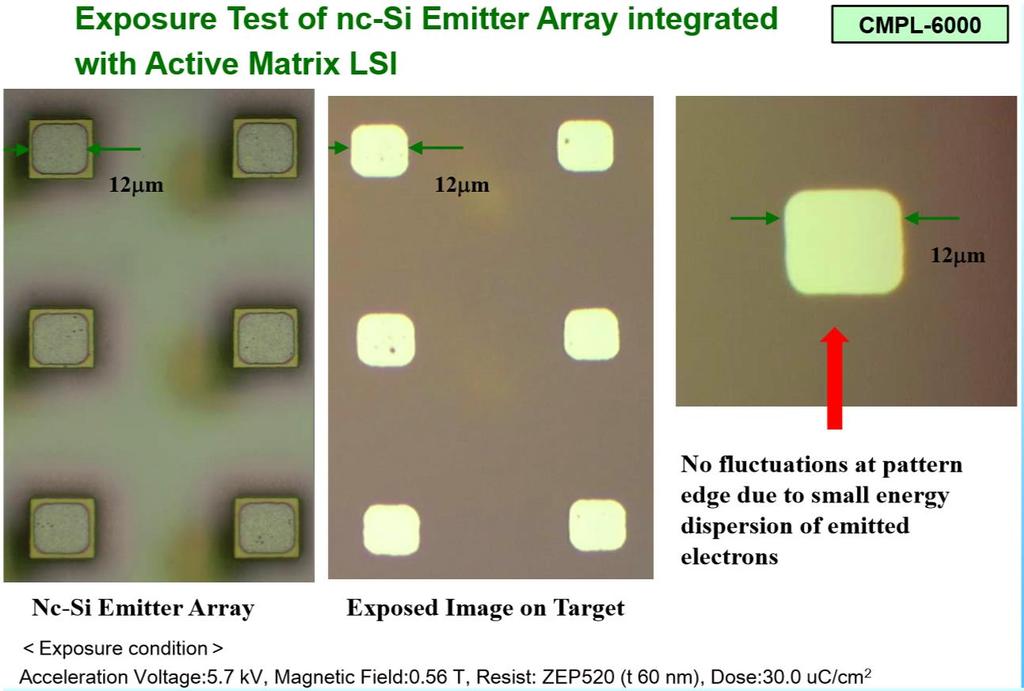
46 New developments 2 New concept: Massively Parallel EBL System based on nc-si emitter array Crestec, Tohoku Univ. and TUAT are jointly developing supported by the Cabinet Office in Japan Massively parallel emitter 47
47 New developments 2 48
 function The grating pitch can be controlled by changing the deflection amplifier gain through the 2nd DA")
48 New developments 3 In optical devices such as DFB laser, pitch grating uniformity and pitch control along the device are critical for optical output and single frequency operation. Pitch control is controlled since several years using the field size modulation ( FSM ) function The grating pitch can be controlled by changing the deflection amplifier gain through the 2nd DA converter. Positioning accuracy is 0.01 nm. Nowadays, the challenging reside in grating uniformity in 1.2 mm cavity lenght DFB lasers, to ensure optical output and single frequency operation, no stitching errors are needed, so the use of 1.2 mm field size is compulsory. Stig&distortion and focus should be corrected. High resolution an accuracy writing for field size wider than 1 mm is been developed for general purpose fabrication 49
49 Thank you for your attention 50
Corporate Introduction of CRESTEC CORPORATION Expert in E-Beam Nanofabrication
 Corporate Introduction of CRESTEC CORPORATION Expert in E-Beam Nanofabrication David López-Romero Moraleda. Technical Support Manager, Crestec Corporation Spain Branch. Financiación-Internacionalización-Cooperación.
Ion Beam Lithography: faster writing strategies for features between 150nm and 1um
 Ion Beam Lithography: faster writing strategies for features between 150nm and 1um Brent P. Gila, Andes Trucco, David Hays Located in sunny Gainesville, FL (100 miles north of Disney World) https://nrf.aux.eng.ufl.edu/
Micro- and Nano-Technology... for Optics
 Micro- and Nano-Technology...... for Optics 3.2 Lithography U.D. Zeitner Fraunhofer Institut für Angewandte Optik und Feinmechanik Jena Printing on Stones Map of Munich Stone Print Contact Printing light
Electron Beam Lithography. Adam Ramm
 Electron Beam Lithography Adam Ramm Why use electrons? Negligible diffraction limitations: R = k λ NA With current optical technology, this equates to about 45nm resolution. For an electron, wavelength
Multi-beam mask writer MBM-1000 for advanced mask making
 Multi-beam mask writer MBM-1000 for advanced mask making H. Matsumoto NuFlare Technology, Inc. Slide 1 Multi-beam Shaping aperture array (SAA) Blanking aperture array (BAA) Sub deflectors Main deflectors
Section 2: Lithography. Jaeger Chapter 2 Litho Reader. The lithographic process
 Section 2: Lithography Jaeger Chapter 2 Litho Reader The lithographic process Photolithographic Process (a) (b) (c) (d) (e) (f) (g) Substrate covered with silicon dioxide barrier layer Positive photoresist
Introduction of New Products
 Field Emission Electron Microscope JEM-3100F For evaluation of materials in the fields of nanoscience and nanomaterials science, TEM is required to provide resolution and analytical capabilities that can
Section 2: Lithography. Jaeger Chapter 2 Litho Reader. EE143 Ali Javey Slide 5-1
 Section 2: Lithography Jaeger Chapter 2 Litho Reader EE143 Ali Javey Slide 5-1 The lithographic process EE143 Ali Javey Slide 5-2 Photolithographic Process (a) (b) (c) (d) (e) (f) (g) Substrate covered
Waveguiding in PMMA photonic crystals
 ROMANIAN JOURNAL OF INFORMATION SCIENCE AND TECHNOLOGY Volume 12, Number 3, 2009, 308 316 Waveguiding in PMMA photonic crystals Daniela DRAGOMAN 1, Adrian DINESCU 2, Raluca MÜLLER2, Cristian KUSKO 2, Alex.
Introduction of ADVANTEST EB Lithography System
 Introduction of ADVANTEST EB Lithography System Nanotechnology Business Division ADVANTEST Corporation 1 2 Node [nm] EB Lithography Products < ADVANTEST s Superiority > High Resolution :EB optical technology
Section 2: Lithography. Jaeger Chapter 2. EE143 Ali Javey Slide 5-1
 Section 2: Lithography Jaeger Chapter 2 EE143 Ali Javey Slide 5-1 The lithographic process EE143 Ali Javey Slide 5-2 Photolithographic Process (a) (b) (c) (d) (e) (f) (g) Substrate covered with silicon
Synthesis of projection lithography for low k1 via interferometry
 Synthesis of projection lithography for low k1 via interferometry Frank Cropanese *, Anatoly Bourov, Yongfa Fan, Andrew Estroff, Lena Zavyalova, Bruce W. Smith Center for Nanolithography Research, Rochester
Fabrication Techniques of Optical ICs
 Fabrication Techniques of Optical ICs Processing Techniques Lift off Process Etching Process Patterning Techniques Photo Lithography Electron Beam Lithography Photo Resist ( Microposit MP1300) Electron
EE143 Fall 2016 Microfabrication Technologies. Lecture 3: Lithography Reading: Jaeger, Chap. 2
 EE143 Fall 2016 Microfabrication Technologies Lecture 3: Lithography Reading: Jaeger, Chap. 2 Prof. Ming C. Wu wu@eecs.berkeley.edu 511 Sutardja Dai Hall (SDH) 1-1 The lithographic process 1-2 1 Photolithographic
Lithographic Performance and Mix-and-Match Lithography using 100 kv Electron Beam System JBX-9300FS
 Lithographic Performance and Mix-and-Match Lithography using 100 kv Electron Beam System JBX-9300FS Yukinori Ochiai, Takashi Ogura, Mitsuru Narihiro, and Kohichi Arai Silicon Systems Research Laboratories,
EG2605 Undergraduate Research Opportunities Program. Large Scale Nano Fabrication via Proton Lithography Using Metallic Stencils
 EG2605 Undergraduate Research Opportunities Program Large Scale Nano Fabrication via Proton Lithography Using Metallic Stencils Tan Chuan Fu 1, Jeroen Anton van Kan 2, Pattabiraman Santhana Raman 2, Yao
Ion Beam Lithography next generation nanofabrication
 Ion Beam Lithography next generation nanofabrication EFUG Bordeaux 2011 ion beams develop Lloyd Peto IBL sales manager Copyright 2011 by Raith GmbH ionline new capabilities You can now Apply an ion beam
Fabrication of Probes for High Resolution Optical Microscopy
 Fabrication of Probes for High Resolution Optical Microscopy Physics 564 Applied Optics Professor Andrès La Rosa David Logan May 27, 2010 Abstract Near Field Scanning Optical Microscopy (NSOM) is a technique
Sub-50 nm period patterns with EUV interference lithography
 Microelectronic Engineering 67 68 (2003) 56 62 www.elsevier.com/ locate/ mee Sub-50 nm period patterns with EUV interference lithography * a, a a b b b H.H. Solak, C. David, J. Gobrecht, V. Golovkina,
A process for, and optical performance of, a low cost Wire Grid Polarizer
 1.0 Introduction A process for, and optical performance of, a low cost Wire Grid Polarizer M.P.C.Watts, M. Little, E. Egan, A. Hochbaum, Chad Jones, S. Stephansen Agoura Technology Low angle shadowed deposition
Major Fabrication Steps in MOS Process Flow
 Major Fabrication Steps in MOS Process Flow UV light Mask oxygen Silicon dioxide photoresist exposed photoresist oxide Silicon substrate Oxidation (Field oxide) Photoresist Coating Mask-Wafer Alignment
Project Staff: Timothy A. Savas, Michael E. Walsh, Thomas B. O'Reilly, Dr. Mark L. Schattenburg, and Professor Henry I. Smith
 9. Interference Lithography Sponsors: National Science Foundation, DMR-0210321; Dupont Agreement 12/10/99 Project Staff: Timothy A. Savas, Michael E. Walsh, Thomas B. O'Reilly, Dr. Mark L. Schattenburg,
Process Optimization
 Process Optimization Process Flow for non-critical layer optimization START Find the swing curve for the desired resist thickness. Determine the resist thickness (spin speed) from the swing curve and find
Supporting Information 1. Experimental
 Supporting Information 1. Experimental The position markers were fabricated by electron-beam lithography. To improve the nanoparticle distribution when depositing aqueous Ag nanoparticles onto the window,
SHAPED E-BEAM NANOPATTERNING WITH PROXIMITY EFFECT CORRECTION
 SHAPED E-BEAM NANOPATTERNING WITH PROXIMITY EFFECT CORRECTION Michal URBANEK a, Vladimir KOLARIK a, Milan MATEJKA a, Frantisek MATEJKA a, Jan BOK a, Petr MIKSIK b, Jan VASINA b a) ISI ASCR,v.v.i., Kralovopolska
Project Staff: Feng Zhang, Prof. Jianfeng Dai (Lanzhou Univ. of Tech.), Prof. Todd Hasting (Univ. Kentucky), Prof. Henry I. Smith
, Prof. Todd Hasting (Univ. Kentucky), Prof. Henry I. Smith") 3. Spatial-Phase-Locked Electron-Beam Lithography Sponsors: No external sponsor Project Staff: Feng Zhang, Prof. Jianfeng Dai (Lanzhou Univ. of Tech.), Prof. Todd Hasting (Univ. Kentucky), Prof. Henry
3. Spatial-Phase-Locked Electron-Beam Lithography Sponsors: No external sponsor Project Staff: Feng Zhang, Prof. Jianfeng Dai (Lanzhou Univ. of Tech.), Prof. Todd Hasting (Univ. Kentucky), Prof. Henry
Results of Proof-of-Concept 50keV electron multi-beam Mask Exposure Tool (emet POC)
") Results of Proof-of-Concept 50keV electron multi-beam Mask Exposure Tool (emet POC) Elmar Platzgummer *, Christof Klein, and Hans Loeschner IMS Nanofabrication AG Schreygasse 3, A-1020 Vienna, Austria
Results of Proof-of-Concept 50keV electron multi-beam Mask Exposure Tool (emet POC) Elmar Platzgummer *, Christof Klein, and Hans Loeschner IMS Nanofabrication AG Schreygasse 3, A-1020 Vienna, Austria
Micro- and Nano-Technology... for Optics
 Micro- and Nano-Technology...... for Optics 3.2 Lithography U.D. Zeitner Fraunhofer Institut für Angewandte Optik und Feinmechanik Jena Printing on Stones Map of Munich Stone Print Shadow Printing Photomask
Functions of the SEM subsystems
 Functions of the SEM subsystems Electronic column It consists of an electron gun and two or more electron lenses, which influence the path of electrons traveling down an evacuated tube. The base of the
Monolithically integrated InGaAs nanowires on 3D. structured silicon-on-insulator as a new platform for. full optical links
 Monolithically integrated InGaAs nanowires on 3D structured silicon-on-insulator as a new platform for full optical links Hyunseok Kim 1, Alan C. Farrell 1, Pradeep Senanayake 1, Wook-Jae Lee 1,* & Diana.
Supplementary Figure 1: Optical Properties of V-shaped Gold Nanoantennas a) Illustration of the possible plasmonic modes.
 Illustration of the possible plasmonic modes.") Supplementary Figure 1: Optical Properties of V-shaped Gold Nanoantennas a) Illustration of the possible plasmonic modes. S- symmetric, AS antisymmetric. b) Calculated linear scattering spectra of individual
Supplementary Figure 1: Optical Properties of V-shaped Gold Nanoantennas a) Illustration of the possible plasmonic modes. S- symmetric, AS antisymmetric. b) Calculated linear scattering spectra of individual
Development of Nanoimprint Mold Using JBX-9300FS
 Development of Nanoimprint Mold Using JBX-9300FS Morihisa Hoga, Mikio Ishikawa, Naoko Kuwahara Tadahiko Takikawa and Shiho Sasaki Dai Nippon Printing Co., Ltd Research & Development Center Electronic Device
plasmonic nanoblock pair
 Nanostructured potential of optical trapping using a plasmonic nanoblock pair Yoshito Tanaka, Shogo Kaneda and Keiji Sasaki* Research Institute for Electronic Science, Hokkaido University, Sapporo 1-2,
EUV Interference Lithography in NewSUBARU
 EUV Interference Lithography in NewSUBARU Takeo Watanabe 1, Tae Geun Kim 2, Yasuyuki Fukushima 1, Noki Sakagami 1, Teruhiko Kimura 1, Yoshito Kamaji 1, Takafumi Iguchi 1, Yuuya Yamaguchi 1, Masaki Tada
(Refer Slide Time: 00:10)
") Fundamentals of optical and scanning electron microscopy Dr. S. Sankaran Department of Metallurgical and Materials Engineering Indian Institute of Technology, Madras Module 03 Unit-6 Instrumental details
Fundamentals of optical and scanning electron microscopy Dr. S. Sankaran Department of Metallurgical and Materials Engineering Indian Institute of Technology, Madras Module 03 Unit-6 Instrumental details
COMPARISON OF ULTIMATE RESOLUTION ACHIEVED BY E-BEAM WRITERS WITH SHAPED BEAM AND WITH GAUSSIAN BEAM
 COMPARISON OF ULTIMATE RESOLUTION ACHIEVED BY E-BEAM WRITERS WITH SHAPED BEAM AND WITH GAUSSIAN BEAM Stanislav KRÁTKÝ a, Vladimír KOLAŘÍK a, Milan MATĚJKA a, Michal URBÁNEK a, Miroslav HORÁČEK a, Jana
GaSb based high power single spatial mode and distributed feedback lasers at 2.0 μm
 GaSb based high power single spatial mode and distributed feedback lasers at 2.0 μm Clifford Frez 1, Kale J. Franz 1, Alexander Ksendzov, 1 Jianfeng Chen 2, Leon Sterengas 2, Gregory L. Belenky 2, Siamak
5. Lithography. 1. photolithography intro: overall, clean room 2. principle 3. tools 4. pattern transfer 5. resolution 6. next-gen
 5. Lithography 1. photolithography intro: overall, clean room 2. principle 3. tools 4. pattern transfer 5. resolution 6. next-gen References: Semiconductor Devices: Physics and Technology. 2 nd Ed. SM
Copyright 2000 by the Society of Photo-Optical Instrumentation Engineers.
 Copyright 2000 by the Society of Photo-Optical Instrumentation Engineers. This paper was published in the proceedings of the 20 th Annual BACUS Symposium on Photomask Technology SPIE Vol. 4186, pp. 503-507.
Lecture 7. Lithography and Pattern Transfer. Reading: Chapter 7
 Lecture 7 Lithography and Pattern Transfer Reading: Chapter 7 Used for Pattern transfer into oxides, metals, semiconductors. 3 types of Photoresists (PR): Lithography and Photoresists 1.) Positive: PR
Lithography. 3 rd. lecture: introduction. Prof. Yosi Shacham-Diamand. Fall 2004
 Lithography 3 rd lecture: introduction Prof. Yosi Shacham-Diamand Fall 2004 1 List of content Fundamental principles Characteristics parameters Exposure systems 2 Fundamental principles Aerial Image Exposure
Design of a high brightness multi-electron-beam source
 vailable online at www.sciencedirect.com Physics Procedia00 1 (2008) 000 000 553 563 www.elsevier.com/locate/procedia www.elsevier.com/locate/xxx Proceedings of the Seventh International Conference on
Machine-Aligned Fabrication of Submicron SIS Tunnel Junctions Using a Focused Ion Beam
 Machine-Aligned Fabrication of Submicron SIS Tunnel Junctions Using a Focused Ion Beam Robert. B. Bass, Jian. Z. Zhang and Aurthur. W. Lichtenberger Department of Electrical Engineering, University of
Zone-plate-array lithography using synchrotron radiation
 Zone-plate-array lithography using synchrotron radiation A. Pépin, a) D. Decanini, and Y. Chen Laboratoire de Microstructures et de Microélectronique (L2M), CNRS, 196 avenue Henri-Ravéra, 92225 Bagneux,
Laser-Produced Sn-plasma for Highvolume Manufacturing EUV Lithography
 Panel discussion Laser-Produced Sn-plasma for Highvolume Manufacturing EUV Lithography Akira Endo * Extreme Ultraviolet Lithography System Development Association Gigaphoton Inc * 2008 EUVL Workshop 11
A Portable Scanning Electron Microscope Column Design Based on the Use of Permanent Magnets
 SCANNING VOL. 20, 87 91 (1998) Received October 8, 1997 FAMS, Inc. Accepted with revision November 9, 1997 A Portable Scanning Electron Microscope Column Design Based on the Use of Permanent Magnets A.
Integrated into Nanowire Waveguides
 Supporting Information Widely Tunable Distributed Bragg Reflectors Integrated into Nanowire Waveguides Anthony Fu, 1,3 Hanwei Gao, 1,3,4 Petar Petrov, 1, Peidong Yang 1,2,3* 1 Department of Chemistry,
Scanning Electron Microscopy SEM. Warren Straszheim, PhD MARL, 23 Town Engineering
 Scanning Electron Microscopy SEM Warren Straszheim, PhD MARL, 23 Town Engineering wesaia@iastate.edu 515-294-8187 How it works Create a focused electron beam Accelerate it Scan it across the sample Map
Optimization of PMMA 950KA4 resist patterns using Electron Beam Lithography
 CeNSE restricted NNFC-TN 2017/001 Technical Note CENSE-NNFC-2017/001 Issued: 03/2017 Optimization of PMMA 950KA4 resist patterns using Electron Beam Lithography Sreedhar Babu, Anita CeNSE, NNFC, Indian
Scanning Electron Microscopy Basics and Applications
 Scanning Electron Microscopy Basics and Applications Dr. Julia Deuschle Stuttgart Center for Electron Microscopy MPI for Solid State Research Room: 1E15, phone: 0711/ 689-1193 email: j.deuschle@fkf.mpg.de
Demo Pattern and Performance Test
 Raith GmbH Hauert 18 Technologiepark D-44227 Dortmund Phone: +49(0)231/97 50 00-0 Fax: +49(0)231/97 50 00-5 Email: postmaster@raith.de Internet: www.raith.com Demo Pattern and Performance Test For Raith
Figure 7 Dynamic range expansion of Shack- Hartmann sensor using a spatial-light modulator
 Figure 4 Advantage of having smaller focal spot on CCD with super-fine pixels: Larger focal point compromises the sensitivity, spatial resolution, and accuracy. Figure 1 Typical microlens array for Shack-Hartmann
OPTI510R: Photonics. Khanh Kieu College of Optical Sciences, University of Arizona Meinel building R.626
 OPTI510R: Photonics Khanh Kieu College of Optical Sciences, University of Arizona kkieu@optics.arizona.edu Meinel building R.626 Announcements Homework #3 is due today No class Monday, Feb 26 Pre-record
Quantized patterning using nanoimprinted blanks
 IOP PUBLISHING Nanotechnology 20 (2009) 155303 (7pp) Quantized patterning using nanoimprinted blanks NANOTECHNOLOGY doi:10.1088/0957-4484/20/15/155303 Stephen Y Chou 1, Wen-Di Li and Xiaogan Liang NanoStructure
Optical Bus for Intra and Inter-chip Optical Interconnects
 Optical Bus for Intra and Inter-chip Optical Interconnects Xiaolong Wang Omega Optics Inc., Austin, TX Ray T. Chen University of Texas at Austin, Austin, TX Outline Perspective of Optical Backplane Bus
Design Rules for Silicon Photonics Prototyping
 Design Rules for licon Photonics Prototyping Version 1 (released February 2008) Introduction IME s Photonics Prototyping Service offers 248nm lithography based fabrication technology for passive licon-on-insulator
Development of a LFLE Double Pattern Process for TE Mode Photonic Devices. Mycahya Eggleston Advisor: Dr. Stephen Preble
 Development of a LFLE Double Pattern Process for TE Mode Photonic Devices Mycahya Eggleston Advisor: Dr. Stephen Preble 2 Introduction and Motivation Silicon Photonics Geometry, TE vs TM, Double Pattern
MICROSTRUCTURING OF METALLIC LAYERS FOR SENSOR APPLICATIONS
 MICROSTRUCTURING OF METALLIC LAYERS FOR SENSOR APPLICATIONS Vladimír KOLAŘÍK, Stanislav KRÁTKÝ, Michal URBÁNEK, Milan MATĚJKA, Jana CHLUMSKÁ, Miroslav HORÁČEK, Institute of Scientific Instruments of the
Part 5-1: Lithography
 Part 5-1: Lithography Yao-Joe Yang 1 Pattern Transfer (Patterning) Types of lithography systems: Optical X-ray electron beam writer (non-traditional, no masks) Two-dimensional pattern transfer: limited
Triple Beam FIB-SEM-Ar(Xe) Combined System NX2000
 Combined System NX2000") SCIENTIFIC INSTRUMENT NEWS 2017 Vol. 8 M A R C H Technical magazine of Electron Microscope and Analytical Instruments. Technical Explanation Triple Beam FIB-SEM-Ar(Xe) Combined System NX2000 Masahiro Kiyohara
SCIENTIFIC INSTRUMENT NEWS 2017 Vol. 8 M A R C H Technical magazine of Electron Microscope and Analytical Instruments. Technical Explanation Triple Beam FIB-SEM-Ar(Xe) Combined System NX2000 Masahiro Kiyohara
Scope and Limit of Lithography to the End of Moore s Law
 Scope and Limit of Lithography to the End of Moore s Law Burn J. Lin tsmc, Inc. 1 What dictate the end of Moore s Law Economy Device limits Lithography limits 2 Litho Requirement of Critical Layers Logic
Fabrication of micro structures on curve surface by X-ray lithography
 Fabrication of micro structures on curve surface by X-ray lithography Yigui Li 1, Susumu Sugiyama 2 Abstract We demonstrate experimentally the x-ray lithography techniques to fabricate micro structures
Microlens formation using heavily dyed photoresist in a single step
 Microlens formation using heavily dyed photoresist in a single step Chris Cox, Curtis Planje, Nick Brakensiek, Zhimin Zhu, Jonathan Mayo Brewer Science, Inc., 2401 Brewer Drive, Rolla, MO 65401, USA ABSTRACT
PICO MASTER 200. UV direct laser writer for maskless lithography
 PICO MASTER 200 UV direct laser writer for maskless lithography 4PICO B.V. Jan Tinbergenstraat 4b 5491 DC Sint-Oedenrode The Netherlands Tel: +31 413 490708 WWW.4PICO.NL 1. Introduction The PicoMaster
Generating integrated-circuit patterns via cutting and stitching of gratings
 Purdue University Purdue e-pubs Birck and NCN Publications Birck Nanotechnology Center 11-2009 Generating integrated-circuit patterns via cutting and stitching of gratings Lin Zhao Purdue University -
5. The Scanning Electron Microscope
 Physical Principles of Electron Microscopy 5. The Scanning Electron Microscope Ray Egerton University of Alberta and National Institute of Nanotechnology Edmonton, Canada www.tem-eels.ca regerton@ualberta.ca
Scanning Electron Microscopy
 Scanning Electron Microscopy For the semiconductor industry A tutorial Titel Vorname Nachname Titel Jobtitle, Bereich/Abteilung Overview Scanning Electron microscopy Scanning Electron Microscopy (SEM)
Comprehensive Simulation of E-beam Lithography Processes Using PROLITH/3D and TEMPTATION Software Tools
 Comprehensive Simulation of E-beam Lithography Processes Using PROLITH/3D and TEMPTATION Software Tools I. Yu. Kuzmin, C. A. Mack* Soft Services, Djalila 5-2-507,Moscow 115580, Russia *FNLE Division ofkla-tencor,
PML2 Projection. Lithography. The mask-less electron multi-beam solution for the 22nm node and beyond. IMS Nanofabrication AG
 SEMATECH Workshop on Maskless Lithography San Francisco, CA Dec 14 2008 PML2 Projection Mask-Less Lithography The mask-less electron multi-beam solution for the 22nm node and beyond AG Projection Mask-Less
Printing Beyond srgb Color Gamut by. Mimicking Silicon Nanostructures in Free-Space
 Supporting Information for: Printing Beyond srgb Color Gamut by Mimicking Silicon Nanostructures in Free-Space Zhaogang Dong 1, Jinfa Ho 1, Ye Feng Yu 2, Yuan Hsing Fu 2, Ramón Paniagua-Dominguez 2, Sihao
NanoSpective, Inc Progress Drive Suite 137 Orlando, Florida
 TEM Techniques Summary The TEM is an analytical instrument in which a thin membrane (typically < 100nm) is placed in the path of an energetic and highly coherent beam of electrons. Typical operating voltages
EE-527: MicroFabrication
 EE-57: MicroFabrication Exposure and Imaging Photons white light Hg arc lamp filtered Hg arc lamp excimer laser x-rays from synchrotron Electrons Ions Exposure Sources focused electron beam direct write
Advanced Device Fabrication Techniques. ChiiDong Chen
 Advanced Device Fabrication Techniques TIGP lecture, NTU 070501 ChiiDong Chen Institute of Physics, Academia Sinica e-mail: chiidong@phys.sinica.edu.tw url: www.phys.sinica.edu.tw/~quela Outline: 1 State-of-the-art
Update on 193nm immersion exposure tool
 Update on 193nm immersion exposure tool S. Owa, H. Nagasaka, Y. Ishii Nikon Corporation O. Hirakawa and T. Yamamoto Tokyo Electron Kyushu Ltd. January 28, 2004 Litho Forum 1 What is immersion lithography?
Lecture 20: Optical Tools for MEMS Imaging
 MECH 466 Microelectromechanical Systems University of Victoria Dept. of Mechanical Engineering Lecture 20: Optical Tools for MEMS Imaging 1 Overview Optical Microscopes Video Microscopes Scanning Electron
Bringing Answers to the Surface
 3D Bringing Answers to the Surface 1 Expanding the Boundaries of Laser Microscopy Measurements and images you can count on. Every time. LEXT OLS4100 Widely used in quality control, research, and development
Helicon mode formation and rf power deposition in a helicon source
 Helicon mode formation and rf power deposition in a helicon source Michael Krämer & Kari Niemi Institut für Experimentalphysik II, Ruhr-Universität D-4478 Bochum, Germany Helicon Mini-Conference APS-DPP,
Optical Proximity Effects
 T h e L i t h o g r a p h y E x p e r t (Spring 1996) Optical Proximity Effects Chris A. Mack, FINLE Technologies, Austin, Texas Proximity effects are the variations in the linewidth of a feature (or the
SCANNING ELECTRON MICROSCOPY AND X-RAY MICROANALYSIS
 SCANNING ELECTRON MICROSCOPY AND X-RAY MICROANALYSIS Robert Edward Lee Electron Microscopy Center Department of Anatomy and Neurobiology Colorado State University P T R Prentice Hall, Englewood Cliffs,
X-ray generation by femtosecond laser pulses and its application to soft X-ray imaging microscope
 X-ray generation by femtosecond laser pulses and its application to soft X-ray imaging microscope Kenichi Ikeda 1, Hideyuki Kotaki 1 ' 2 and Kazuhisa Nakajima 1 ' 2 ' 3 1 Graduate University for Advanced
Lecture 13 Basic Photolithography
 Lecture 13 Basic Photolithography Chapter 12 Wolf and Tauber 1/64 Announcements Homework: Homework 3 is due today, please hand them in at the front. Will be returned one week from Thursday (16 th Nov).
2. Pulsed Acoustic Microscopy and Picosecond Ultrasonics
 1st International Symposium on Laser Ultrasonics: Science, Technology and Applications July 16-18 2008, Montreal, Canada Picosecond Ultrasonic Microscopy of Semiconductor Nanostructures Thomas J GRIMSLEY
Narrow line diode laser stacks for DPAL pumping
 Narrow line diode laser stacks for DPAL pumping Tobias Koenning David Irwin, Dean Stapleton, Rajiv Pandey, Tina Guiney, Steve Patterson DILAS Diode Laser Inc. Joerg Neukum Outline Company overview Standard
Georgia Tech IEN EBL Facility NNIN Highlights 2014 External User Projects
 Georgia Tech IEN EBL Facility NNIN Highlights 2014 External User Projects Silicon based Photonic Crystal Devices Silicon based photonic crystal devices are ultra-small photonic devices that can confine
450mm patterning out of darkness Backend Process Exposure Tool SOKUDO Lithography Breakfast Forum July 10, 2013 Doug Shelton Canon USA Inc.
 450mm patterning out of darkness Backend Process Exposure Tool SOKUDO Lithography Breakfast Forum 2013 July 10, 2013 Doug Shelton Canon USA Inc. Introduction Half Pitch [nm] 2013 2014 2015 2016 2017 2018
Feature-level Compensation & Control
 Feature-level Compensation & Control 2 Sensors and Control Nathan Cheung, Kameshwar Poolla, Costas Spanos Workshop 11/19/2003 3 Metrology, Control, and Integration Nathan Cheung, UCB SOI Wafers Multi wavelength
CHAPTER 2 POLARIZATION SPLITTER- ROTATOR BASED ON A DOUBLE- ETCHED DIRECTIONAL COUPLER
 CHAPTER 2 POLARIZATION SPLITTER- ROTATOR BASED ON A DOUBLE- ETCHED DIRECTIONAL COUPLER As we discussed in chapter 1, silicon photonics has received much attention in the last decade. The main reason is
A Parallel Radial Mirror Energy Analyzer Attachment for the Scanning Electron Microscope
 142 doi:10.1017/s1431927615013288 Microscopy Society of America 2015 A Parallel Radial Mirror Energy Analyzer Attachment for the Scanning Electron Microscope Kang Hao Cheong, Weiding Han, Anjam Khursheed
MEMS for RF, Micro Optics and Scanning Probe Nanotechnology Applications
 MEMS for RF, Micro Optics and Scanning Probe Nanotechnology Applications Part I: RF Applications Introductions and Motivations What are RF MEMS? Example Devices RFIC RFIC consists of Active components
Micro-Optic Solar Concentration and Next-Generation Prototypes
 Micro-Optic Solar Concentration and Next-Generation Prototypes Jason H. Karp, Eric J. Tremblay and Joseph E. Ford Photonics Systems Integration Lab University of California San Diego Jacobs School of Engineering
Measurement of Microscopic Three-dimensional Profiles with High Accuracy and Simple Operation
 238 Hitachi Review Vol. 65 (2016), No. 7 Featured Articles Measurement of Microscopic Three-dimensional Profiles with High Accuracy and Simple Operation AFM5500M Scanning Probe Microscope Satoshi Hasumura
Optical Lithography. Here Is Why. Burn J. Lin SPIE PRESS. Bellingham, Washington USA
 Optical Lithography Here Is Why Burn J. Lin SPIE PRESS Bellingham, Washington USA Contents Preface xiii Chapter 1 Introducing Optical Lithography /1 1.1 The Role of Lithography in Integrated Circuit Fabrication
Lithography. Development of High-Quality Attenuated Phase-Shift Masks
 Lithography S P E C I A L Development of High-Quality Attenuated Phase-Shift Masks by Toshihiro Ii and Masao Otaki, Toppan Printing Co., Ltd. Along with the year-by-year acceleration of semiconductor device
Scanning electron microscope
 Scanning electron microscope 6 th CEMM workshop Maja Koblar, Sc. Eng. Physics Outline The basic principle? What is an electron? Parts of the SEM Electron gun Electromagnetic lenses Apertures Chamber and
DOE Project: Resist Characterization
 DOE Project: Resist Characterization GOAL To achieve high resolution and adequate throughput, a photoresist must possess relatively high contrast and sensitivity to exposing radiation. The objective of
Supporting Information. Filter-free image sensor pixels comprising silicon. nanowires with selective color absorption
 Supporting Information Filter-free image sensor pixels comprising silicon nanowires with selective color absorption Hyunsung Park, Yaping Dan,, Kwanyong Seo,, Young J. Yu, Peter K. Duane, Munib Wober,
Scanning electron microscope
 Scanning electron microscope 5 th CEMM workshop Maja Koblar, Sc. Eng. Physics Outline The basic principle? What is an electron? Parts of the SEM Electron gun Electromagnetic lenses Apertures Detectors
Chapter 3 Fabrication
 Chapter 3 Fabrication The total structure of MO pick-up contains four parts: 1. A sub-micro aperture underneath the SIL The sub-micro aperture is used to limit the final spot size from 300nm to 600nm for
Photolithography Technology and Application
 Photolithography Technology and Application Jeff Tsai Director, Graduate Institute of Electro-Optical Engineering Tatung University Art or Science? Lind width = 100 to 5 micron meter!! Resolution = ~ 3
Quasi-Phase-Matched Faraday Rotation in Semiconductor Waveguides with a Magneto-Optic Cladding for Monolithically Integrated Optical Isolators
 Quasi-Phase-Matched Faraday Rotation in Semiconductor Waveguides with a Magneto-Optic Cladding for Monolithically Integrated Optical Isolators Prof. David C. Hutchings, Barry M. Holmes and Cui Zhang, Acknowledgements