Micro- and Nano- Fabrication and Replication Techniques
|
|
|
- Sheena Golden
- 5 years ago
- Views:
Transcription
1 Micro- and Nano- Fabrication and Replication Techniques
2 Why do we have to write thing small and replicate fast?

3 Plenty of Room at the Bottom Richard P. Feynman, December 1959 How do we write it? We have no standard technique to do this now. But let me argue that it is not as difficult as it first appears to be. We can reverse the lenses of the electron microscope in order to demagnify as well as magnify. A source of ions, sent through the microscope lenses in reverse, could be focused to a very small spot. We could write with that spot like we write in a TV cathode ray oscilloscope, by going across in lines, and having an adjustment which determines the amount of material which is going to be deposited as we scan in lines. This method might be very slow because of space charge limitations. There will be more rapid methods. We could first make, perhaps by some photo process, a screen which has holes in it in the form of the letters. Then we would strike an arc behind the holes and draw metallic ions through the holes; then we could again use our system of lenses and make a small image in the form of ions, which would deposit the metal on the pin.
4 Plenty of Room at the Bottom Richard P. Feynman, December 1959 A simpler way might be this (though I am not sure it would work): We take light and, through an optical microscope running backwards, we focus it onto a very small photoelectric screen. Then electrons come away from the screen where the light is shining. These electrons are focused down in size by the electron microscope lenses to impinge directly upon the surface of the metal. Will such a beam etch away the metal if it is run long enough? I don't know. If it doesn't work for a metal surface, it must be possible to find some surface with which to coat the original pin so that, where the electrons bombard, a change is made which we could recognize later.
5 Plenty of Room at the Bottom Richard P. Feynman, December 1959 There is no intensity problem in these devices---not what you are used to in magnification, where you have to take a few electrons and spread them over a bigger and bigger screen; it is just the opposite. The light which we get from a page is concentrated onto a very small area so it is very intense. The few electrons which come from the photoelectric screen are demagnified down to a very tiny area so that, again, they are very intense. I don't know why this hasn't been done yet!


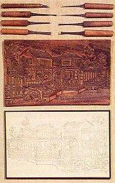
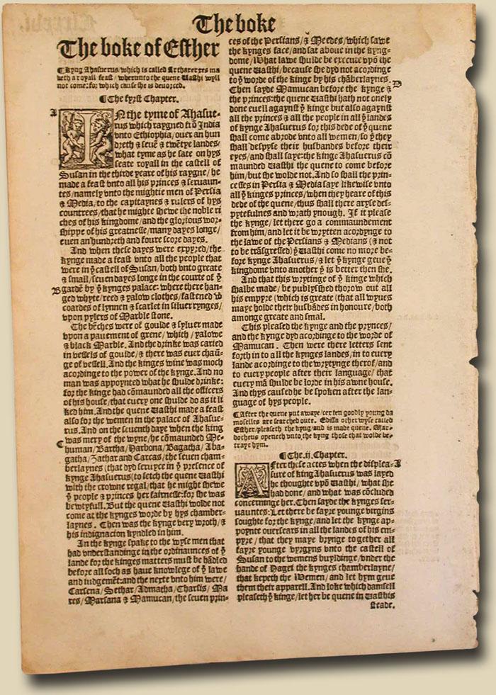
6 Ancient Patterning "This is the Elks' land". A greeting at the mouth of Dalbergsaa, Southern Dal. It seems that the carvings of Northern Scandinavia's including Kola Peninsula are the oldest. Large figures of ritual animals characterise the Mesolithic period mostly before c.4200 BC


7 Writing by Inks Writing Brush ~2000 Ys Quill Pen ~1000 Ys
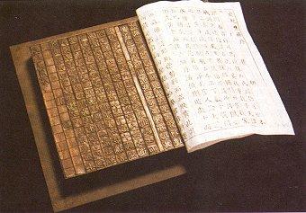
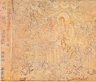
8 Chinese Replication and 1048
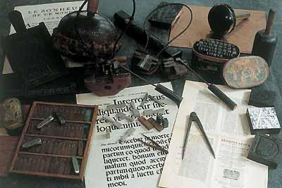
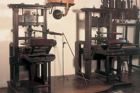
9 Western Replication

10 Building a computer


11 First Integrated Circuit "What we didn't realize then was that the integrated circuit would reduce the cost of electronic functions by a factor of a million to one, nothing had ever done that for anything before" - Jack Kilby 2000 Nobel Prize 1958 Texas Instruments


12 metal-oxide-semiconductor fieldeffect transistor (MOSET)
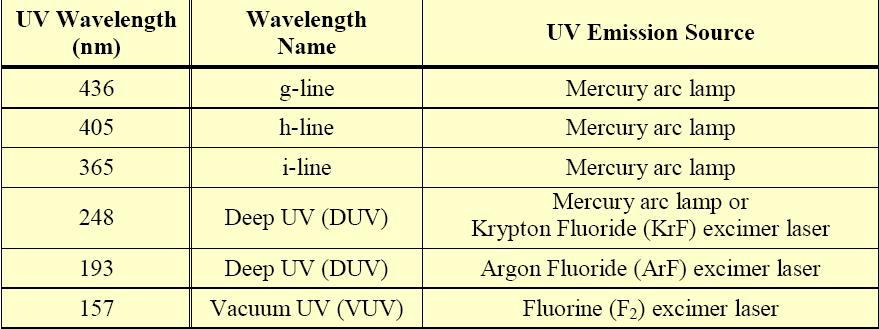
13 Fabrication Techniques Laser writing E-beam writing Focus ion beam writing Nonlinear optical writing Interference lithography Dip-pen lithography SPM lithography
14 Replication Techniques Photolithography X-ray or e-beam projection Microcontact printing (soft-lithography) Nanoimprint

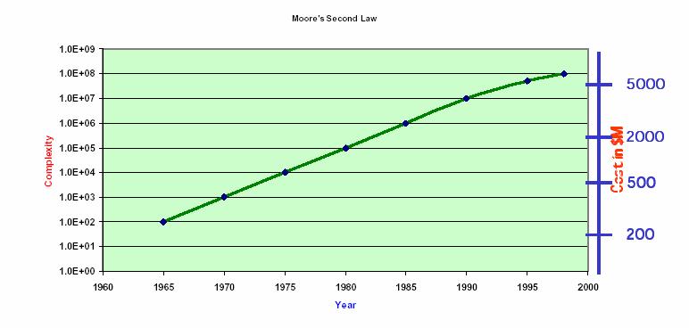
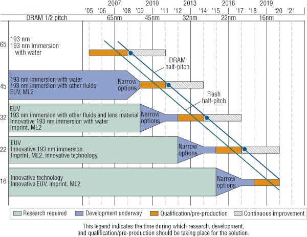
15 Moore s Law
16 Tool Cost
17
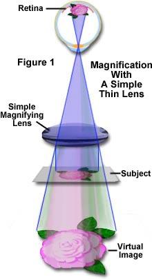
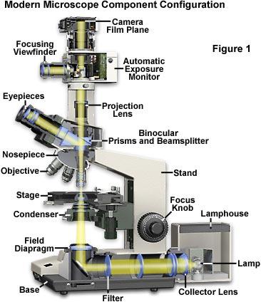
18 Optical Microscope
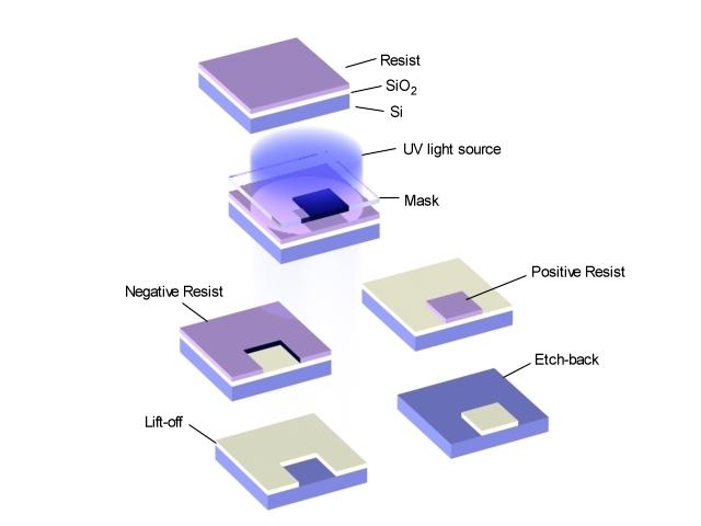
19 Methods of Photolithography


20 Limit of Photolithography r = 1.22 x λ/(2 x N.A.) N.A. = n x sin(θ)
 Depth of Focus = λ/(n.a.) 2 K = 0.")
21 Diffraction Limit Resolution = K x λ/(n.a.) Depth of Focus = λ/(n.a.) 2 K = 0.61
22 Photolithography

23
24 Water Immersion Lithography Resolution (R) = K x λ/(n.a.) K = 0.25, NA ~1.4, λ = 193 R = 35 nm Air n= Water n = 1.437
25
26 Photolithography Process
27 RCA Cleaning (By Radio Corporation of America in 1965) Chemicals Volume ratio Procedure Time (min) Operation Temperature Function Trichlorothane 5 Room T Dissolve Organic Acetone 5 Room T Dissolve Organic DI Water 5 Room T Washing H 2 SO 4 (98%)-H 2 O 2 (30%) (Piranha Solution) 3: ~90 Oxide and Dissolve Organic and Metals DI Water 5 Room T Washing HF(49 wt %)-H 2 O ~2: Room T Dissolve surface Si0 2 NH 4 OH(29%)-H 2 O 2 (30%)- H 2 O 1:1: ~90 Oxide and Dissolve Metals DI Water 5 Room T Washing HCl(37%)- H 2 O 2 (30%)- H 2 O 1:1: ~90 Oxide and Dissolve Metals DI Water 5 Room T Washing Spin Dry (In lad N 2 blow )
28 Positive tone Negative tone


29 1 Spin Coating Photoresist on Wafer c.c PR on the Wafer Choose the Spin Speed to control the thickness 2 Photo resist:shipley 1813 Spin: 2000 rpm 5 s 4500 rpm 15 s Soft Bake: s Exposure:7 s Wait for 5 to 15 second Developed:MF319 for 15 s

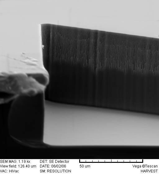
30 Standard Mask Size: 5 5


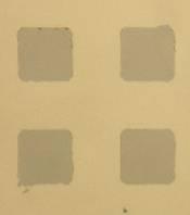
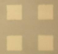
31 Align the pattern and Exposure UV light Off Align the pattern UV light On


 SU-8")

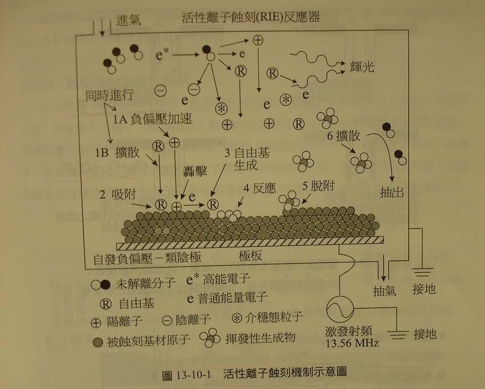
32 Some Photoresist Need PEB (post exposure Bake) SU , 60 s 95, 60 s SPR 510A 90, 90 s


33 Develop the Photoresist Photo resist:shipley 1813 Spin: 2000 rpm 5 s 4500 rpm 15 s Soft Bake: s Exposure:7 s Developed:MF319 for 15 s


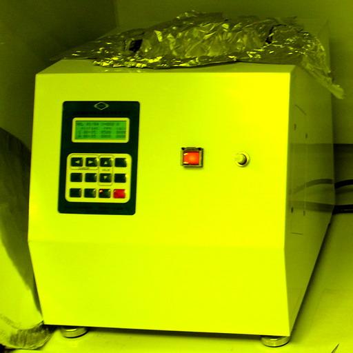
34 黃光室的黃光是很重要的
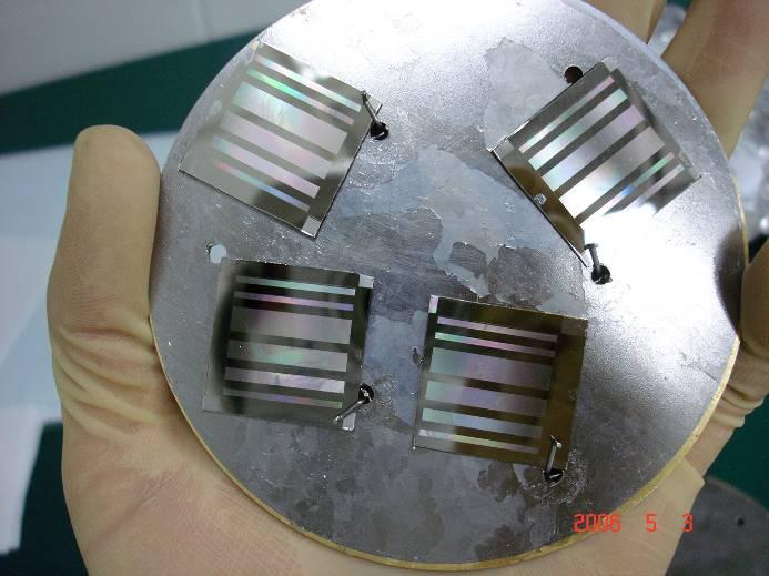
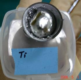
35 TI 50 nm

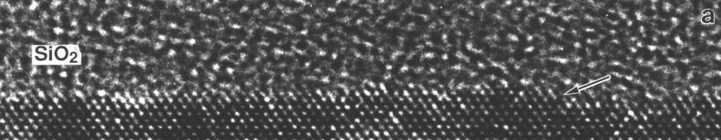
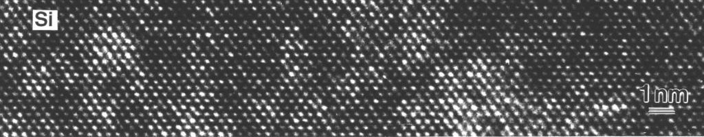
36 SEM image of Ti 50 nm on Si wafer

37 Lift OFF PROCESS BY ACETONE

38 Ti 50 nm LIFT OFF


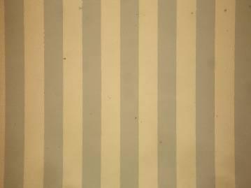
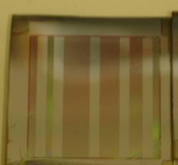
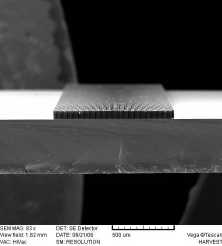
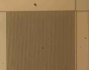
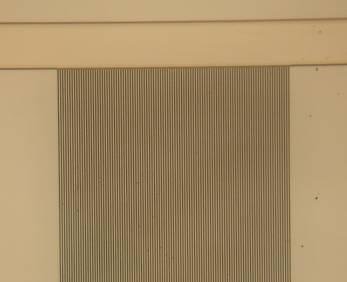
39 Ti 50 nm on Si 20 um Ti S1813 Si Si S1813 Si Ti Si


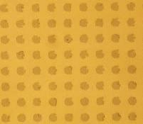
40 Ti 50 nm on Si 5 um S1813 Si Ti Si
41 ICP- BOSCH Recipe Etching & Sidewall Passivation Cycle RF SF 6 plasma (a) Etch Step PR or Metal Si substrate RF CF X plasma (b) Passivate Step PR or Metal Si substrate RF SF 6 plasma PR or Metal (a ) Etch Step Si substrate
42 RF SF 6 plasma The gases in RCAS C 4 F 8, CF 4, CHF 3, Ar, O 2 RF CF X plasma SAMCO ICP (RECIPE) Si etching CF 4 / O 2 = 30 / 10 SiO 2 ( on Si )CHF 3 / Ar = 15 / 30 The gases in NEMSRC RF SF 6 plasma SF 6, C 4 F 8, CF 4, O 2 RECIPE TIME Etch: 11.5 s SF 6 (130sccm) O 2 (13sccm) Passivate: 7s C 4 F 8 (85sccm)

43 RCAS E-Beam Evaporator 一儀器名稱中文名稱 : 電子束蒸鍍系統英文名稱 :E-Beam 二. 儀器廠牌 型號及儀器購置年限廠牌 : 聚昌科技 AST 儀器購置年限 : 民國 92 年 7 月三. 重要規格蒸鍍金屬 : Ni Ti Au Al Pt Cr
44 TI 50 nm
45


46
47

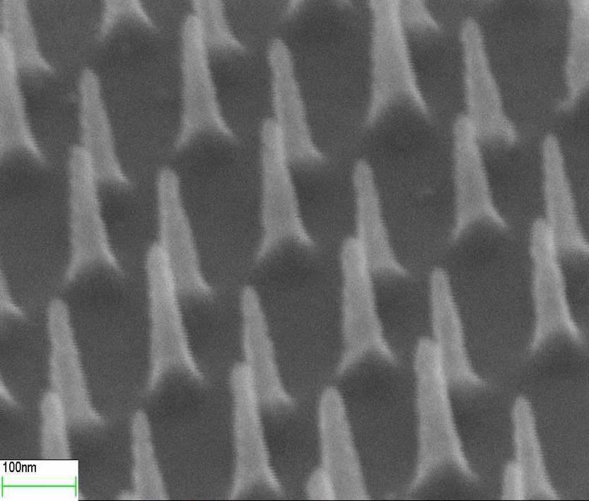
48 NEMSRC ICP 51.2 um
49 Si ---S ICP

 O 2 (13sccm)")
50 NEMSRC ICP :S1813 on Si The gases in NEMSRC SF 6, C 4 F 8, CF 4, O 2 RECIPE TIME Etch: 11.5 s SF 6 (130sccm) O 2 (13sccm) Passivate: 7s C 4 F 8 (85sccm) 51.2 um

 O 2 (13sccm)")
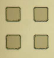
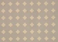
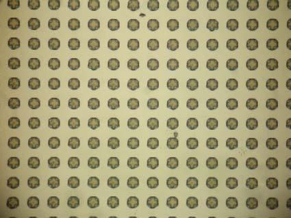
51 NEMSRC ICP :S1813 on Si --20μm array The gases in NEMSRC SF 6, C 4 F 8, CF 4, O 2 RECIPE TIME Etch: 11.5 s SF 6 (130sccm) O 2 (13sccm) Passivate: 7s C 4 F 8 (85sccm)

 O 2 (13sccm)")
52 NEMSRC ICP :S1813 on Si --20μm array The gases in NEMSRC SF 6, C 4 F 8, CF 4, O 2 RECIPE TIME Etch: 11.5 s SF 6 (130sccm) O 2 (13sccm) Passivate: 7s C 4 F 8 (85sccm)

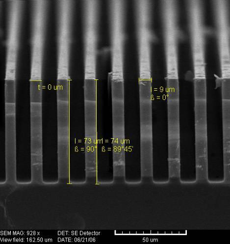
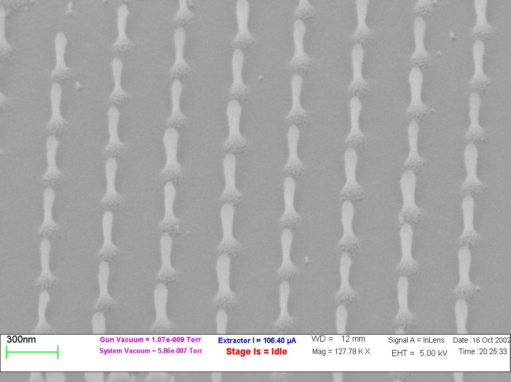
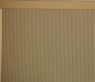
53 NEMSRC ICP Si 10 um Line

 O 2 (13sccm)")
54 The gases in NEMSRC SF 6, C 4 F 8, CF 4, O 2 NEMSRC ICP :S1813 on Si 10 um pillar RECIPE TIME Etch: 11.5 s SF 6 (130sccm) O 2 (13sccm) Passivate: 7s C 4 F 8 (85sccm)

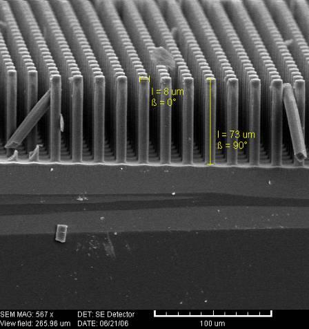
55 NEMSRC ICP Si 10 um pillar

56 Si 5um Line

 O 2 (13sccm)")
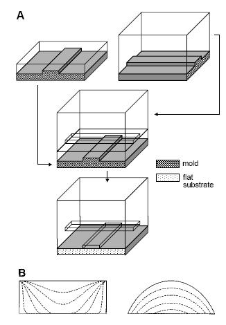
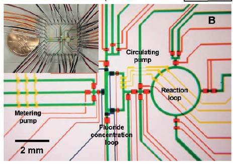
57 The gases in NEMSRC SF 6, C 4 F 8, CF 4, O 2 NEMSRC ICP :S1813 on Si 5 um pillar RECIPE TIME Etch: 11.5 s SF 6 (130sccm) O 2 (13sccm) Passivate: 7s C 4 F 8 (85sccm)

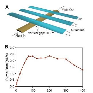
 O 2 (13sccm)")
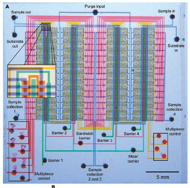
58 The gases in NEMSRC SF 6, C 4 F 8, CF 4, O 2 NEMSRC ICP :S1813 on Si 5 um pillar RECIPE TIME Etch: 11.5 s SF 6 (130sccm) O 2 (13sccm) Passivate: 7s C 4 F 8 (85sccm)

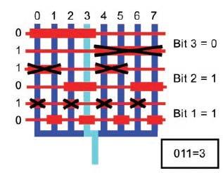
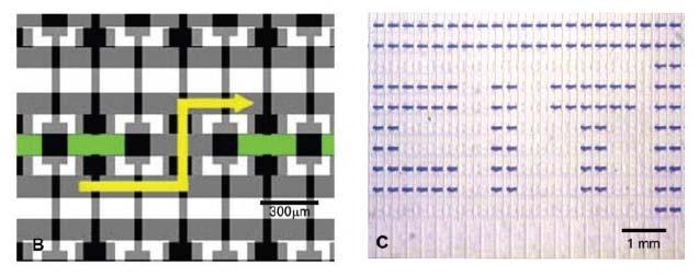
 O 2 (13sccm)")
59 The gases in NEMSRC SF 6, C 4 F 8, CF 4, O 2 NEMSRC ICP :S1813 on Si 5 um pillar RECIPE TIME Etch: 11.5 s SF 6 (130sccm) O 2 (13sccm) Passivate: 7s C 4 F 8 (85sccm)
60
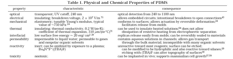
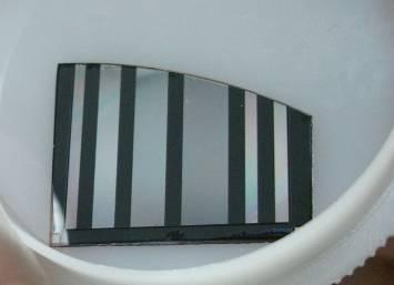
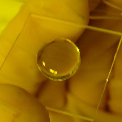
61 PDMS
62
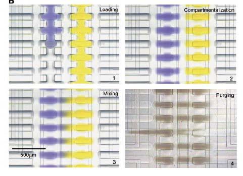
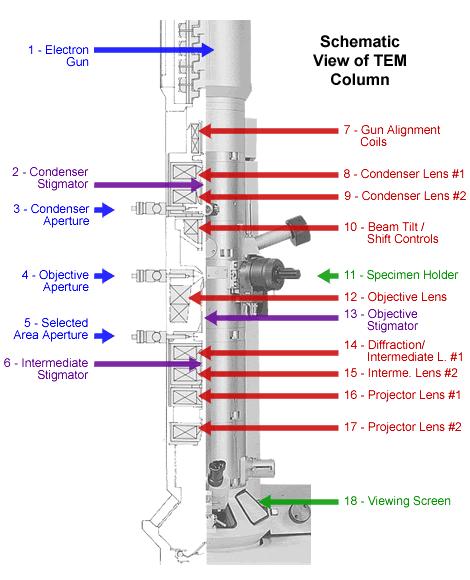
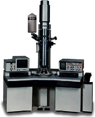
63 Microfluidics by Soft Lithography


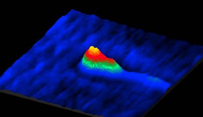
64 Microfluidics by Soft Lithography
65 Microfluidics by Soft Lithography

66 Microfluidics by Soft Lithography

67
68
69


70

71 Microfabricated Fluidic System by Soft Lithography

72 Peristaltic Pump by Soft Lithography

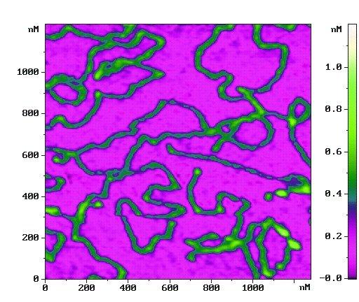
73 Fluidic Control by Microfabricated Valves
74 Addressable Microfluidic System
 2500 2000 1500 1000 500 0 1E-3 7.5E-4 5E-4 2.5E-4 1.25E-4 6.25E-5 300 400 500 600 700 800 Wavelength (nm) Intensity (a.u.) 5000 4000 3000 2000 1000 0 5 10 15 20 25 30 Conc.")
75 Integrated Detection System in Microchannel Abs Wavelength (nm) fluidic channel + microlens + fiber 0 Intensity (a.u.) E-3 7.5E-4 5E-4 2.5E E E Wavelength (nm) Intensity (a.u.) Conc.
76 Reference

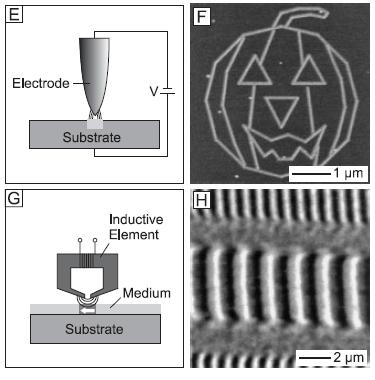
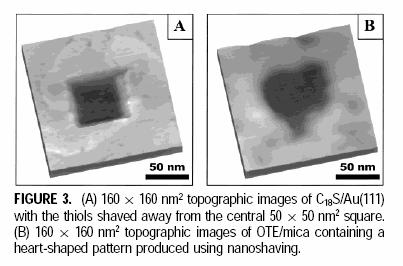
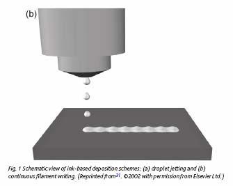
77 Direct Writing

78
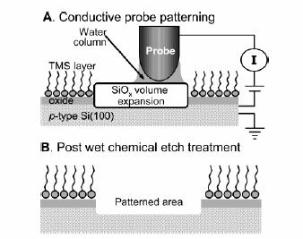
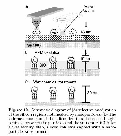
79 Electron Microscope
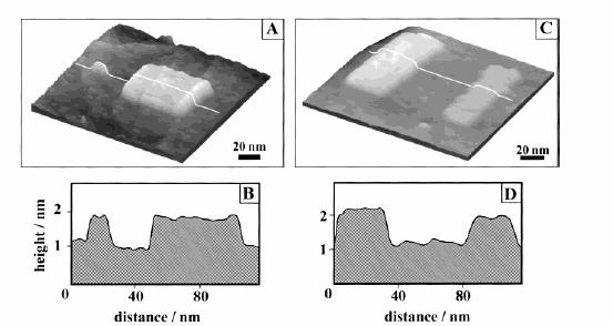
80 TEM Image

81 E-Beam Lithography


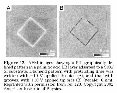
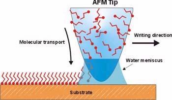
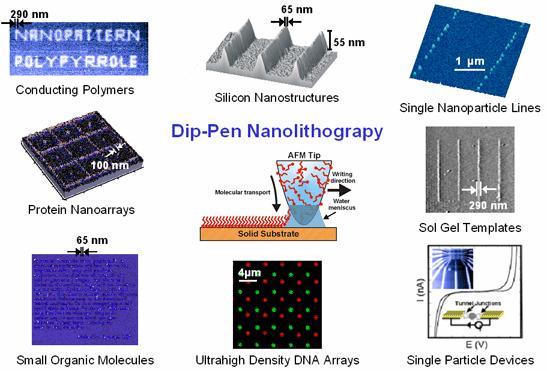
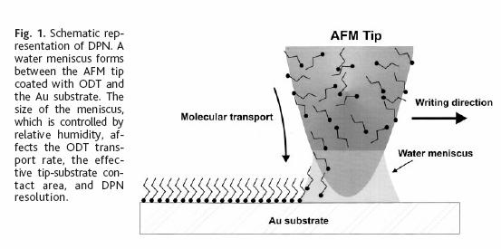
82 E-beam Writer Better than 10 nm lines over 4 inch wafer
83 EUV System

84 Two Photon Writing

85 Two Photon Writing

86 Two Photon Writing

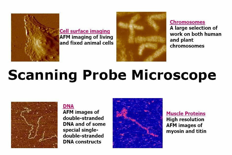
87 Introduction To Scanning Probe Microscopy

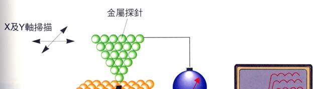
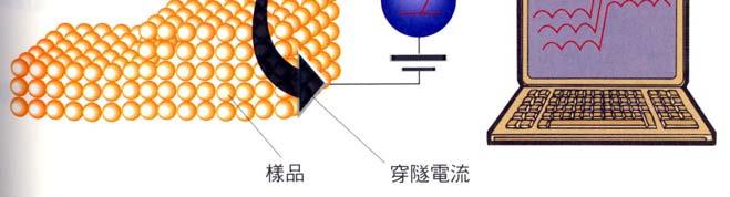
88 Scanning Tunneling Microscopy


89 STM Images Polymer Gold atom

90 Atomic Force Microscopy
91


92 AFM Images E Coli Protein Nanotubes DNA

93 Scanning Probe Family

94 STM Lithography Resist: Thiol
95 STM Lithography

96 Oxidation Lithography
97 AFM Lithography

98 Substitution Lithography
99 Dip-Pen Lithography

100
101 Dip-Pen Lithography
102 Dip-Pen Lithography
103 Dip-pen Lithography
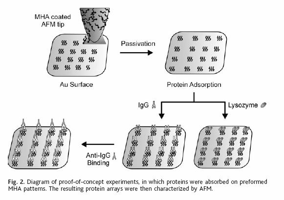
104

105
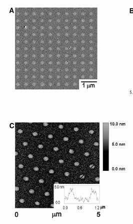
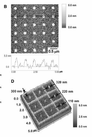
106
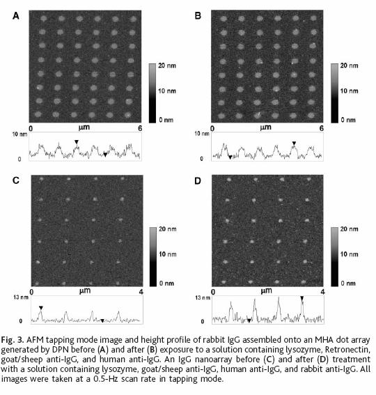
107
108

109 Dip-Pen Array
110 Ultimate STM Lithography

111 Single Atomic Manipulation
112 Single Molecular Vibrational Spectra by STM

113 Building Molecule Step by Step

114 Atomic Manipulation

115 Near-Field Microscope
116 Near-Field Images DNA Nanosphere Sperm

117 Near-Field Lithography

118 Add on Writing

119 Direct Writing 3D

120 Direct Writing
121

122 Direct Writing

123 Inkjet Printer

124 Inkjet Printing


125 Inkjet Printing

126 Inkjet Printing

127 Inkjet Printing

128 Replication
129 Align the pattern and Exposure UV light Off Align the pattern UV light On
130 Stepper
131 E-beam Projection

132

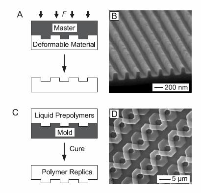
133 Nanoimprint Lithography Mold PMMA Substrate Imprint Remove Mold RIE Evaporation Lift-off
134

135 Step and Flash Imprint Lithography

136 NX-2000, Nanoimprintor, Nanonex Nanoimprintors

137 Imprinting Result
138 Challenges Mask Fabrication (1:1) Lift-off process Resist Mask Design
Micro- and Nano- Fabrication and Replication Techniques
 Micro- and Nano- Fabrication and Replication Techniques Why do we have to write thing small and replicate fast? Plenty of Room at the Bottom Richard P. Feynman, December 1959 How do we write it? We have
Part 5-1: Lithography
 Part 5-1: Lithography Yao-Joe Yang 1 Pattern Transfer (Patterning) Types of lithography systems: Optical X-ray electron beam writer (non-traditional, no masks) Two-dimensional pattern transfer: limited
Section 2: Lithography. Jaeger Chapter 2 Litho Reader. The lithographic process
 Section 2: Lithography Jaeger Chapter 2 Litho Reader The lithographic process Photolithographic Process (a) (b) (c) (d) (e) (f) (g) Substrate covered with silicon dioxide barrier layer Positive photoresist
Section 2: Lithography. Jaeger Chapter 2 Litho Reader. EE143 Ali Javey Slide 5-1
 Section 2: Lithography Jaeger Chapter 2 Litho Reader EE143 Ali Javey Slide 5-1 The lithographic process EE143 Ali Javey Slide 5-2 Photolithographic Process (a) (b) (c) (d) (e) (f) (g) Substrate covered
Major Fabrication Steps in MOS Process Flow
 Major Fabrication Steps in MOS Process Flow UV light Mask oxygen Silicon dioxide photoresist exposed photoresist oxide Silicon substrate Oxidation (Field oxide) Photoresist Coating Mask-Wafer Alignment
Chapter 3 Fabrication
 Chapter 3 Fabrication The total structure of MO pick-up contains four parts: 1. A sub-micro aperture underneath the SIL The sub-micro aperture is used to limit the final spot size from 300nm to 600nm for
EE143 Fall 2016 Microfabrication Technologies. Lecture 3: Lithography Reading: Jaeger, Chap. 2
 EE143 Fall 2016 Microfabrication Technologies Lecture 3: Lithography Reading: Jaeger, Chap. 2 Prof. Ming C. Wu wu@eecs.berkeley.edu 511 Sutardja Dai Hall (SDH) 1-1 The lithographic process 1-2 1 Photolithographic
5. Lithography. 1. photolithography intro: overall, clean room 2. principle 3. tools 4. pattern transfer 5. resolution 6. next-gen
 5. Lithography 1. photolithography intro: overall, clean room 2. principle 3. tools 4. pattern transfer 5. resolution 6. next-gen References: Semiconductor Devices: Physics and Technology. 2 nd Ed. SM
Lecture 7. Lithography and Pattern Transfer. Reading: Chapter 7
 Lecture 7 Lithography and Pattern Transfer Reading: Chapter 7 Used for Pattern transfer into oxides, metals, semiconductors. 3 types of Photoresists (PR): Lithography and Photoresists 1.) Positive: PR
Clean Room Technology Optical Lithography. Lithography I. takenfrombdhuey
 Clean Room Technology Optical Lithography Lithography I If the automobile had followed the same development cycle as the computer, a Rolls Royce would today cost $100, get a million miles per gallon, and
Nanoscale Lithography. NA & Immersion. Trends in λ, NA, k 1. Pushing The Limits of Photolithography Introduction to Nanotechnology
 15-398 Introduction to Nanotechnology Nanoscale Lithography Seth Copen Goldstein Seth@cs.cmu.Edu CMU Pushing The Limits of Photolithography Reduce wavelength (λ) Use Reducing Lens Increase Numerical Aperture
NanoFabrication Kingston. Seminar and Webinar January 31, 2017 Rob Knobel Associate Professor, Dept. of Physics Queen s University
 NanoFabrication Kingston Seminar and Webinar January 31, 2017 Rob Knobel Associate Professor, Dept. of Physics Queen s University What is NFK? It s a place, an team of experts and a service. The goal of
Photolithography Technology and Application
 Photolithography Technology and Application Jeff Tsai Director, Graduate Institute of Electro-Optical Engineering Tatung University Art or Science? Lind width = 100 to 5 micron meter!! Resolution = ~ 3
Module - 2 Lecture - 13 Lithography I
 Nano Structured Materials-Synthesis, Properties, Self Assembly and Applications Prof. Ashok. K.Ganguli Department of Chemistry Indian Institute of Technology, Delhi Module - 2 Lecture - 13 Lithography
Semiconductor Manufacturing Technology. Semiconductor Manufacturing Technology. Photolithography: Resist Development and Advanced Lithography
 Semiconductor Manufacturing Technology Michael Quirk & Julian Serda October 2001 by Prentice Hall Chapter 15 Photolithography: Resist Development and Advanced Lithography Eight Basic Steps of Photolithography
Section 2: Lithography. Jaeger Chapter 2. EE143 Ali Javey Slide 5-1
 Section 2: Lithography Jaeger Chapter 2 EE143 Ali Javey Slide 5-1 The lithographic process EE143 Ali Javey Slide 5-2 Photolithographic Process (a) (b) (c) (d) (e) (f) (g) Substrate covered with silicon
Institute of Solid State Physics. Technische Universität Graz. Lithography. Peter Hadley
 Technische Universität Graz Institute of Solid State Physics Lithography Peter Hadley http://www.cleanroom.byu.edu/virtual_cleanroom.parts/lithography.html http://www.cleanroom.byu.edu/su8.phtml Spin coater
Photolithography I ( Part 1 )
") 1 Photolithography I ( Part 1 ) Chapter 13 : Semiconductor Manufacturing Technology by M. Quirk & J. Serda Bjørn-Ove Fimland, Department of Electronics and Telecommunication, Norwegian University of Science
1 Photolithography I ( Part 1 ) Chapter 13 : Semiconductor Manufacturing Technology by M. Quirk & J. Serda Bjørn-Ove Fimland, Department of Electronics and Telecommunication, Norwegian University of Science
Supplementary Materials for
 www.sciencemag.org/cgi/content/full/science.1234855/dc1 Supplementary Materials for Taxel-Addressable Matrix of Vertical-Nanowire Piezotronic Transistors for Active/Adaptive Tactile Imaging Wenzhuo Wu,
write-nanocircuits Direct-write Jaebum Joo and Joseph M. Jacobson Molecular Machines, Media Lab Massachusetts Institute of Technology, Cambridge, MA
 Fab-in in-a-box: Direct-write write-nanocircuits Jaebum Joo and Joseph M. Jacobson Massachusetts Institute of Technology, Cambridge, MA April 17, 2008 Avogadro Scale Computing / 1 Avogadro number s? Intel
Dr. Dirk Meyners Prof. Wagner. Wagner / Meyners Micro / Nanosystems Technology
 Micro/Nanosystems Technology Dr. Dirk Meyners Prof. Wagner 1 Outline - Lithography Overview - UV-Lithography - Resolution Enhancement Techniques - Electron Beam Lithography - Patterning with Focused Ion
PHGN/CHEN/MLGN 435/535: Interdisciplinary Silicon Processing Laboratory. Simple Si solar Cell!
 Where were we? Simple Si solar Cell! Two Levels of Masks - photoresist, alignment Etch and oxidation to isolate thermal oxide, deposited oxide, wet etching, dry etching, isolation schemes Doping - diffusion/ion
MICRO AND NANOPROCESSING TECHNOLOGIES
 MICRO AND NANOPROCESSING TECHNOLOGIES LECTURE 4 Optical lithography Concepts and processes Lithography systems Fundamental limitations and other issues Photoresists Photolithography process Process parameter
EG2605 Undergraduate Research Opportunities Program. Large Scale Nano Fabrication via Proton Lithography Using Metallic Stencils
 EG2605 Undergraduate Research Opportunities Program Large Scale Nano Fabrication via Proton Lithography Using Metallic Stencils Tan Chuan Fu 1, Jeroen Anton van Kan 2, Pattabiraman Santhana Raman 2, Yao
Device Fabrication: Photolithography
 Device Fabrication: Photolithography 1 Objectives List the four components of the photoresist Describe the difference between +PR and PR Describe a photolithography process sequence List four alignment
Machine-Aligned Fabrication of Submicron SIS Tunnel Junctions Using a Focused Ion Beam
 Machine-Aligned Fabrication of Submicron SIS Tunnel Junctions Using a Focused Ion Beam Robert. B. Bass, Jian. Z. Zhang and Aurthur. W. Lichtenberger Department of Electrical Engineering, University of
Quantized patterning using nanoimprinted blanks
 IOP PUBLISHING Nanotechnology 20 (2009) 155303 (7pp) Quantized patterning using nanoimprinted blanks NANOTECHNOLOGY doi:10.1088/0957-4484/20/15/155303 Stephen Y Chou 1, Wen-Di Li and Xiaogan Liang NanoStructure
Module 11: Photolithography. Lecture 14: Photolithography 4 (Continued)
") Module 11: Photolithography Lecture 14: Photolithography 4 (Continued) 1 In the previous lecture, we have discussed the utility of the three printing modes, and their relative advantages and disadvantages.
Module 11: Photolithography Lecture 14: Photolithography 4 (Continued) 1 In the previous lecture, we have discussed the utility of the three printing modes, and their relative advantages and disadvantages.
Lecture 8. Microlithography
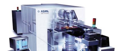
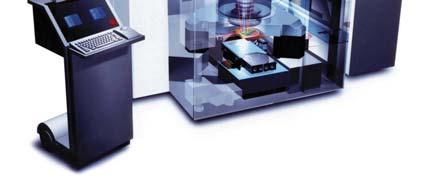
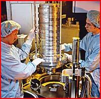
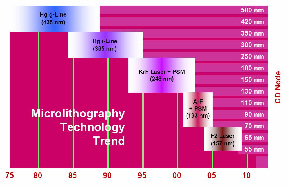
 Lecture 8 Microlithography Lithography Introduction Process Flow Wafer Exposure Systems Masks Resists State of the Art Lithography Next Generation Lithography (NGL) Recommended videos: http://www.youtube.com/user/asmlcompany#p/search/1/jh6urfqt_d4
CHAPTER 2 Principle and Design
 CHAPTER 2 Principle and Design The binary and gray-scale microlens will be designed and fabricated. Silicon nitride and photoresist will be taken as the material of the microlens in this thesis. The design
Micro- and Nano-Technology... for Optics
 Micro- and Nano-Technology...... for Optics 3.2 Lithography U.D. Zeitner Fraunhofer Institut für Angewandte Optik und Feinmechanik Jena Printing on Stones Map of Munich Stone Print Contact Printing light
Lecture 13 Basic Photolithography
 Lecture 13 Basic Photolithography Chapter 12 Wolf and Tauber 1/64 Announcements Homework: Homework 3 is due today, please hand them in at the front. Will be returned one week from Thursday (16 th Nov).
Supplementary information for Stretchable photonic crystal cavity with
 Supplementary information for Stretchable photonic crystal cavity with wide frequency tunability Chun L. Yu, 1,, Hyunwoo Kim, 1, Nathalie de Leon, 1,2 Ian W. Frank, 3 Jacob T. Robinson, 1,! Murray McCutcheon,
Supporting Information 1. Experimental
 Supporting Information 1. Experimental The position markers were fabricated by electron-beam lithography. To improve the nanoparticle distribution when depositing aqueous Ag nanoparticles onto the window,
Low-power carbon nanotube-based integrated circuits that can be transferred to biological surfaces
 SUPPLEMENTARY INFORMATION Articles https://doi.org/10.1038/s41928-018-0056-6 In the format provided by the authors and unedited. Low-power carbon nanotube-based integrated circuits that can be transferred
2.1 BASIC THEORY: INTERFERENCE OF TWO BEAMS
 2 LASER INTERFERENCE LITHOGRAPHY (LIL) 9 2 LASER INTERFERENCE LITHOGRAPHY (LIL) Laser interference lithography [3~22] (LIL) is a method to produce periodic structures using two interfering highly-coherent
Nanostencil Lithography and Nanoelectronic Applications
 Microsystems Laboratory Nanostencil Lithography and Nanoelectronic Applications Oscar Vazquez, Marc van den Boogaart, Dr. Lianne Doeswijk, Prof. Juergen Brugger, LMIS1 Dr. Chan Woo Park, Visiting Professor
Strategies for low cost imprint molds
 Strategies for low cost imprint molds M.P.C. Watts, Impattern Solutions, 9404 Bell Mountain Drive Austin TX 78730 www.impattern.com ABSTRACT The Cost of ownership (COO) due to the mold can be minimized
MICROSTRUCTURING OF METALLIC LAYERS FOR SENSOR APPLICATIONS
 MICROSTRUCTURING OF METALLIC LAYERS FOR SENSOR APPLICATIONS Vladimír KOLAŘÍK, Stanislav KRÁTKÝ, Michal URBÁNEK, Milan MATĚJKA, Jana CHLUMSKÁ, Miroslav HORÁČEK, Institute of Scientific Instruments of the
Lithography Is the Designer s Brush. Lithography is indispensible for defining locations and configurations of circuit elements/functions.
 Lithography 1 Lithography Is the Designer s Brush Lithography is indispensible for defining locations and configurations of circuit elements/functions. 2 ITRS 2007 The major challenge in litho: CD, CD
POLYMER MICROSTRUCTURE WITH TILTED MICROPILLAR ARRAY AND METHOD OF FABRICATING THE SAME
 POLYMER MICROSTRUCTURE WITH TILTED MICROPILLAR ARRAY AND METHOD OF FABRICATING THE SAME Field of the Invention The present invention relates to a polymer microstructure. In particular, the present invention
Soft Electronics Enabled Ergonomic Human-Computer Interaction for Swallowing Training
 Supplementary Information Soft Electronics Enabled Ergonomic Human-Computer Interaction for Swallowing Training Yongkuk Lee 1,+, Benjamin Nicholls 2,+, Dong Sup Lee 1, Yanfei Chen 3, Youngjae Chun 3,4,
Supplementary Information
 Supplementary Information Wireless thin film transistor based on micro magnetic induction coupling antenna Byoung Ok Jun 1, Gwang Jun Lee 1, Jong Gu Kang 1,2, Seung Uk Kim 1, Ji Woong Choi 1, Seung Nam
KMPR 1010 Process for Glass Wafers
 KMPR 1010 Process for Glass Wafers KMPR 1010 Steps Protocol Step System Condition Note Plasma Cleaning PVA Tepla Ion 10 5 mins Run OmniCoat Receipt Dehydration Any Heat Plate 150 C, 5 mins HMDS Coating
SUPPLEMENTARY INFORMATION
 SUPPLEMENTARY INFORMATION doi:10.1038/nature11293 1. Formation of (111)B polar surface on Si(111) for selective-area growth of InGaAs nanowires on Si. Conventional III-V nanowires (NWs) tend to grow in
Developments, Applications and Challenges for the Industrial Implementation of Nanoimprint Lithography
 Developments, Applications and Challenges for the Industrial Implementation of Nanoimprint Lithography Martin Eibelhuber, Business Development Manager m.eibelhuber@evgroup.com Outline Introduction Imprint
DTU DANCHIP an open access micro/nanofabrication facility bridging academic research and small scale production
 DTU DANCHIP an open access micro/nanofabrication facility bridging academic research and small scale production DTU Danchip National Center for Micro- and Nanofabrication DTU Danchip DTU Danchip is Denmark
A BASIC EXPERIMENTAL STUDY OF CAST FILM EXTRUSION PROCESS FOR FABRICATION OF PLASTIC MICROLENS ARRAY DEVICE
 A BASIC EXPERIMENTAL STUDY OF CAST FILM EXTRUSION PROCESS FOR FABRICATION OF PLASTIC MICROLENS ARRAY DEVICE Chih-Yuan Chang and Yi-Min Hsieh and Xuan-Hao Hsu Department of Mold and Die Engineering, National
FINDINGS. REU Student: Philip Garcia Graduate Student Mentor: Anabil Chaudhuri Faculty Mentor: Steven R. J. Brueck. Figure 1
 FINDINGS REU Student: Philip Garcia Graduate Student Mentor: Anabil Chaudhuri Faculty Mentor: Steven R. J. Brueck A. Results At the Center for High Tech Materials at the University of New Mexico, my work
Micro-Nanofabrication
 Zheng Cui Micro-Nanofabrication TECHNOLOGIES AND APPLICATIONS ^f**"?* ö Springer Higher Education Press -T O Table of Content Preface About the Author Chapter 1 Introduction 1 1.1 Micro-nanotechnologies
State-of-the-art device fabrication techniques
 State-of-the-art device fabrication techniques! Standard Photo-lithography and e-beam lithography! Advanced lithography techniques used in semiconductor industry Deposition: Thermal evaporation, e-gun
Nanofluidic Diodes based on Nanotube Heterojunctions
 Supporting Information Nanofluidic Diodes based on Nanotube Heterojunctions Ruoxue Yan, Wenjie Liang, Rong Fan, Peidong Yang 1 Department of Chemistry, University of California, Berkeley, CA 94720, USA
FABRICATION OF CMOS INTEGRATED CIRCUITS. Dr. Mohammed M. Farag
 FABRICATION OF CMOS INTEGRATED CIRCUITS Dr. Mohammed M. Farag Outline Overview of CMOS Fabrication Processes The CMOS Fabrication Process Flow Design Rules Reference: Uyemura, John P. "Introduction to
Fabrication Techniques of Optical ICs
 Fabrication Techniques of Optical ICs Processing Techniques Lift off Process Etching Process Patterning Techniques Photo Lithography Electron Beam Lithography Photo Resist ( Microposit MP1300) Electron
Ion Beam Lithography next generation nanofabrication
 Ion Beam Lithography next generation nanofabrication EFUG Bordeaux 2011 ion beams develop Lloyd Peto IBL sales manager Copyright 2011 by Raith GmbH ionline new capabilities You can now Apply an ion beam
Chapter 6. Photolithography
 Chapter 6 Photolithography 2006/4/10 1 Objectives List the four components of the photoresist Describe the difference between +PR and PR Describe a photolithography process sequence List four alignment
Rapid and inexpensive fabrication of polymeric microfluidic devices via toner transfer masking
 Easley et al. Toner Transfer Masking Page -1- B816575K_supplementary_revd.doc December 3, 2008 Supplementary Information for Rapid and inexpensive fabrication of polymeric microfluidic devices via toner
Module 11: Photolithography. Lecture11: Photolithography - I
 Module 11: Photolithography Lecture11: Photolithography - I 1 11.0 Photolithography Fundamentals We will all agree that incredible progress is happening in the filed of electronics and computers. For example,
i- Line Photoresist Development: Replacement Evaluation of OiR
 i- Line Photoresist Development: Replacement Evaluation of OiR 906-12 Nishtha Bhatia High School Intern 31 July 2014 The Marvell Nanofabrication Laboratory s current i-line photoresist, OiR 897-10i, has
Microlens formation using heavily dyed photoresist in a single step
 Microlens formation using heavily dyed photoresist in a single step Chris Cox, Curtis Planje, Nick Brakensiek, Zhimin Zhu, Jonathan Mayo Brewer Science, Inc., 2401 Brewer Drive, Rolla, MO 65401, USA ABSTRACT
ECSE 6300 IC Fabrication Laboratory Lecture 3 Photolithography. Lecture Outline
 ECSE 6300 IC Fabrication Laboratory Lecture 3 Photolithography Prof. James J. Q. Lu Bldg. CII, Rooms 6229 Rensselaer Polytechnic Institute Troy, NY 12180 Tel. (518)276 2909 e mails: luj@rpi.edu http://www.ecse.rpi.edu/courses/s18/ecse
3.Photolithography and resist systems
 3.Photolithography and resist systems Exposure Mercury arc lamp Shadow printing projection printing Photomask Substrates Resist systems DNQ-Novolak-based Epoxy-based Polyimide based 1 Exposure Mercury
Photolithography II ( Part 2 )
") 1 Photolithography II ( Part 2 ) Chapter 14 : Semiconductor Manufacturing Technology by M. Quirk & J. Serda Saroj Kumar Patra, Department of Electronics and Telecommunication, Norwegian University of Science
1 Photolithography II ( Part 2 ) Chapter 14 : Semiconductor Manufacturing Technology by M. Quirk & J. Serda Saroj Kumar Patra, Department of Electronics and Telecommunication, Norwegian University of Science
32nm High-K/Metal Gate Version Including 2nd Generation Intel Core processor family
 From Sand to Silicon Making of a Chip Illustrations 32nm High-K/Metal Gate Version Including 2nd Generation Intel Core processor family April 2011 1 The illustrations on the following foils are low resolution
Development of a LFLE Double Pattern Process for TE Mode Photonic Devices. Mycahya Eggleston Advisor: Dr. Stephen Preble
 Development of a LFLE Double Pattern Process for TE Mode Photonic Devices Mycahya Eggleston Advisor: Dr. Stephen Preble 2 Introduction and Motivation Silicon Photonics Geometry, TE vs TM, Double Pattern
EE 143 Microfabrication Technology Fall 2014
 EE 143 Microfabrication Technology Fall 2014 Prof. Clark T.-C. Nguyen Dept. of Electrical Engineering & Computer Sciences University of California at Berkeley Berkeley, CA 94720 EE 143: Microfabrication
Atlas 46 novel negative tone photoresist which combines the good properties of the established SU-8 and CAR 44
 EIPBN, 30 th Mai 2018 Atlas 46 novel negative tone photoresist which combines the good properties of the established SU-8 and CAR 44 Dr. Christian Kaiser, Matthias Schirmer Allresist GmbH, Germany Outline
University of Minnesota Nano Fabrication Center Standard Operating Procedure Equipment Name:
 Equipment Name: Coral Name: Nanoimprinter Revision Number: 1.1 Model: NX-B200 Revisionist: M. Fisher Location: Bay 4 Date: 2/12/2010 1 Description Nanonex NX-B200 nanoimprinter is another method of transfer
MEMS for RF, Micro Optics and Scanning Probe Nanotechnology Applications
 MEMS for RF, Micro Optics and Scanning Probe Nanotechnology Applications Part I: RF Applications Introductions and Motivations What are RF MEMS? Example Devices RFIC RFIC consists of Active components
Micro- and Nano-Technology... for Optics
 Micro- and Nano-Technology...... for Optics 3.2 Lithography U.D. Zeitner Fraunhofer Institut für Angewandte Optik und Feinmechanik Jena Printing on Stones Map of Munich Stone Print Shadow Printing Photomask
Optical Bus for Intra and Inter-chip Optical Interconnects
 Optical Bus for Intra and Inter-chip Optical Interconnects Xiaolong Wang Omega Optics Inc., Austin, TX Ray T. Chen University of Texas at Austin, Austin, TX Outline Perspective of Optical Backplane Bus
SYNTHESIS AND CHARACTERIZATION OF II-IV GROUP AND SILICON RELATED NANOMATERIALS
 SYNTHESIS AND CHARACTERIZATION OF II-IV GROUP AND SILICON RELATED NANOMATERIALS ISMATHULLAKHAN SHAFIQ MASTER OF PHILOSOPHY CITY UNIVERSITY OF HONG KONG FEBRUARY 2008 CITY UNIVERSITY OF HONG KONG 香港城市大學
Photolithography 光刻 Part I: Optics
 微纳光电子材料与器件工艺原理 Photolithography 光刻 Part I: Optics Xing Sheng 盛兴 Department of Electronic Engineering Tsinghua University xingsheng@tsinghua.edu.cn 1 Integrate Circuits Moore's law transistor number transistor
Polymer optical waveguide based bi-directional optical bus architecture for high speed optical backplane
 Polymer optical waveguide based bi-directional optical bus architecture for high speed optical backplane Xiaohui Lin a, Xinyuan Dou a, Alan X. Wang b and Ray T. Chen 1,*, Fellow, IEEE a Department of Electrical
High Spectral Resolution Plasmonic Color Filters with Subwavelength Dimensions Supplemental Information
 High Spectral Resolution Plasmonic Color Filters with Subwavelength Dimensions Supplemental Information Dagny Fleischman 1, Katherine T. Fountaine 2, Colton R. Bukowsky 1, Giulia Tagliabue 1, Luke A. Sweatlock
Fabrication of suspended micro-structures using diffsuser lithography on negative photoresist
 Journal of Mechanical Science and Technology 22 (2008) 1765~1771 Journal of Mechanical Science and Technology www.springerlink.com/content/1738-494x DOI 10.1007/s12206-008-0601-8 Fabrication of suspended
Monolithically integrated InGaAs nanowires on 3D. structured silicon-on-insulator as a new platform for. full optical links
 Monolithically integrated InGaAs nanowires on 3D structured silicon-on-insulator as a new platform for full optical links Hyunseok Kim 1, Alan C. Farrell 1, Pradeep Senanayake 1, Wook-Jae Lee 1,* & Diana.
Nanotechnology I+II 2006 / 07
 Nanotechnology for engineers Winter semester 2006-2007 Nanotechnology I+II 2006 / 07 Juergen Brugger & Patrik Hoffmann & Teams Course agenda (winter semester) Nanotechnology I winter semester (23.10.06-9.2.06)
PROFILE CONTROL OF A BOROSILICATE-GLASS GROOVE FORMED BY DEEP REACTIVE ION ETCHING. Teruhisa Akashi and Yasuhiro Yoshimura
 Stresa, Italy, 25-27 April 2007 PROFILE CONTROL OF A BOROSILICATE-GLASS GROOVE FORMED BY DEEP REACTIVE ION ETCHING Teruhisa Akashi and Yasuhiro Yoshimura Mechanical Engineering Research Laboratory (MERL),
Outline. 1 Introduction. 2 Basic IC fabrication processes. 3 Fabrication techniques for MEMS. 4 Applications. 5 Mechanics issues on MEMS MDL NTHU
 Outline 1 Introduction 2 Basic IC fabrication processes 3 Fabrication techniques for MEMS 4 Applications 5 Mechanics issues on MEMS 2.2 Lithography Reading: Runyan Chap. 5, or 莊達人 Chap. 7, or Wolf and
Design Rules for Silicon Photonics Prototyping
 Design Rules for licon Photonics Prototyping Version 1 (released February 2008) Introduction IME s Photonics Prototyping Service offers 248nm lithography based fabrication technology for passive licon-on-insulator
A process for, and optical performance of, a low cost Wire Grid Polarizer
 1.0 Introduction A process for, and optical performance of, a low cost Wire Grid Polarizer M.P.C.Watts, M. Little, E. Egan, A. Hochbaum, Chad Jones, S. Stephansen Agoura Technology Low angle shadowed deposition
Process Optimization
 Process Optimization Process Flow for non-critical layer optimization START Find the swing curve for the desired resist thickness. Determine the resist thickness (spin speed) from the swing curve and find
MICROCHIP MANUFACTURING by S. Wolf
 MICROCHIP MANUFACTURING by S. Wolf Chapter 19 LITHOGRAPHY II: IMAGE-FORMATION and OPTICAL HARDWARE 2004 by LATTICE PRESS CHAPTER 19 - CONTENTS Preliminaries: Wave- Motion & The Behavior of Light Resolution
photolithographic techniques (1). Molybdenum electrodes (50 nm thick) are deposited by
. Molybdenum electrodes (50 nm thick) are deposited by") Supporting online material Materials and Methods Single-walled carbon nanotube (SWNT) devices are fabricated using standard photolithographic techniques (1). Molybdenum electrodes (50 nm thick) are deposited
Supporting online material Materials and Methods Single-walled carbon nanotube (SWNT) devices are fabricated using standard photolithographic techniques (1). Molybdenum electrodes (50 nm thick) are deposited
Welcome to. A facility within the Nanometer Structure Consortium (nmc) at Lund University. nanolab. lund
 at Lund University. nanolab. lund") lund nanolab Welcome to A facility within the Nanometer Structure Consortium (nmc) at Lund University »It s a dream come true. This is the lab I always dreamt of. I didn t know it would ever exist.«ivan
lund nanolab Welcome to A facility within the Nanometer Structure Consortium (nmc) at Lund University »It s a dream come true. This is the lab I always dreamt of. I didn t know it would ever exist.«ivan
EE4800 CMOS Digital IC Design & Analysis. Lecture 1 Introduction Zhuo Feng
 EE4800 CMOS Digital IC Design & Analysis Lecture 1 Introduction Zhuo Feng 1.1 Prof. Zhuo Feng Office: EERC 730 Phone: 487-3116 Email: zhuofeng@mtu.edu Class Website http://www.ece.mtu.edu/~zhuofeng/ee4800fall2010.html
Lecture 20: Optical Tools for MEMS Imaging
 MECH 466 Microelectromechanical Systems University of Victoria Dept. of Mechanical Engineering Lecture 20: Optical Tools for MEMS Imaging 1 Overview Optical Microscopes Video Microscopes Scanning Electron
College of Engineering Department of Electrical Engineering and Computer Sciences University of California, Berkeley
 College of Engineering Department of Electrical Engineering and Below are your weekly quizzes. You should print out a copy of the quiz and complete it before your lab section. Bring in the completed quiz
Optical Issues in Photolithography
 OpenStax-CNX module: m25448 1 Optical Issues in Photolithography Andrew R. Barron This work is produced by OpenStax-CNX and licensed under the Creative Commons Attribution License 3.0 note: This module
Nano-structured superconducting single-photon detector
 Nano-structured superconducting single-photon detector G. Gol'tsman *a, A. Korneev a,v. Izbenko a, K. Smirnov a, P. Kouminov a, B. Voronov a, A. Verevkin b, J. Zhang b, A. Pearlman b, W. Slysz b, and R.
Pattern Transfer CD-AFM. Resist Features on Poly. Poly Features on Oxide. Quate Group, Stanford University
 Resist Features on Poly Pattern Transfer Poly Features on Oxide CD-AFM The Critical Dimension AFM Boot -Shaped Tip Tip shape is optimized to sense topography on vertical surfaces Two-dimensional feedback
Lithography. 3 rd. lecture: introduction. Prof. Yosi Shacham-Diamand. Fall 2004
 Lithography 3 rd lecture: introduction Prof. Yosi Shacham-Diamand Fall 2004 1 List of content Fundamental principles Characteristics parameters Exposure systems 2 Fundamental principles Aerial Image Exposure
Figure 7 Dynamic range expansion of Shack- Hartmann sensor using a spatial-light modulator
 Figure 4 Advantage of having smaller focal spot on CCD with super-fine pixels: Larger focal point compromises the sensitivity, spatial resolution, and accuracy. Figure 1 Typical microlens array for Shack-Hartmann
FABRICATION AND CHARACTERIZATION FOR InAs QUANTUM DOTS IN GaAs SOLAR CELLS.
 FABRICATION AND CHARACTERIZATION FOR InAs QUANTUM DOTS IN GaAs SOLAR CELLS. REU program, University at New Mexico Center for High Technology Materials August, 2011 Student: Thao Nguyen Mentor: Prof. Luke
AC : EXPERIMENTAL MODULES INTRODUCING MICRO- FABRICATION UTILIZING A MULTIDISCIPLINARY APPROACH
 AC 2011-1595: EXPERIMENTAL MODULES INTRODUCING MICRO- FABRICATION UTILIZING A MULTIDISCIPLINARY APPROACH Shawn Wagoner, Binghamton University Director, Nanofabrication Labatory at Binghamton University,
Coating of Si Nanowire Array by Flexible Polymer
 , pp.422-426 http://dx.doi.org/10.14257/astl.2016.139.84 Coating of Si Nanowire Array by Flexible Polymer Hee- Jo An 1, Seung-jin Lee 2, Taek-soo Ji 3* 1,2.3 Department of Electronics and Computer Engineering,
January, 2004 Jeju Island. Acknowledgements OTFL
 High-Speed Fabrication of Nanostructures using Atomic Force Microscope Lithography Haiwon Lee Department of Chemistry US-Korea NanoForum 02/17, 2005 January, 2004 Jeju Island Acknowledgements Contents
Nanotechnology, the infrastructure, and IBM s research projects
 Nanotechnology, the infrastructure, and IBM s research projects Dr. Paul Seidler Coordinator Nanotechnology Center, IBM Research - Zurich Nanotechnology is the understanding and control of matter at dimensions
EE-527: MicroFabrication
 EE-57: MicroFabrication Exposure and Imaging Photons white light Hg arc lamp filtered Hg arc lamp excimer laser x-rays from synchrotron Electrons Ions Exposure Sources focused electron beam direct write