Critical Factors in Thru Hole Defects By Ernie Grice Vice President of Sales Kurtz Ersa North America
|
|
|
- Deirdre Bruce
- 5 years ago
- Views:
Transcription

1 Critical Factors in Thru Hole Defects By Ernie Grice Vice President of Sales Kurtz Ersa North America Production needs us

2 Soldering Zone Production needs us

3 Thru Hole Soldering Challenges Seite 3


4 Selective solder masks High potential for defects! 7 mm! Small but deep Cut-outs are requiring a higher wave. Effect: More turbulent wave with more dross creation. Difficult to control the contact time => higher failure rate can be expected Solution from Ersa: Programmable wave height in the solder program. Seite 4

5 Selectiv Solder Masks lead free wave process! Seite 5
6 Typical Thru Hole Defects: Bridging Component Orientation, Lead Length, Pitch, Design Topside Hole Fill Layer Count, Thermal Demand, Lead to Hole Ratio, Design Solder Balls Flux and solder mask Insufficient Solder Flux, Contamination All of These factors can be resolved and more easily managed with Selective Soldering. Seite 6
7 Content Thermal Demand Fundamentals and the Physics of Solder Joints Thick Copper Technologies PCB Layout - Theory and Practice of Heat Traps Soldering defects Preheating Process Soldering Trials Parameters and Results Conclusion Seite 7

8 What is a Good Quality Joint? Goal: 100% Through hole filling Seite 8
9 Target conditions of the IPC A 610 Target Class 1, 2, 3 There is 100% fill This is easy to inspect, there is no cause for any speculation Seite 9


10 Acceptable conditions of the IPC A 610 Acceptable Class 1, 2, 3 Minimum 75% fill Question: How to inspect 75%?? Seite 10


11 Error Pattern insufficient solder and possible consequences Seite 11

12 core conditions at a solder joint to achieve good quality Heat capacity Seite 12
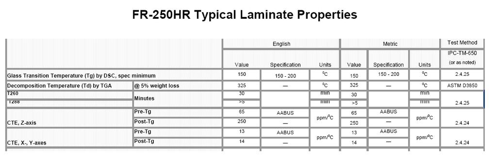
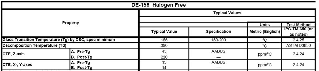
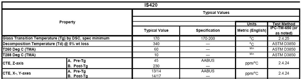
13 Glasübergangstemperatur T G /734 F /644 F /617 F Seite 13
* T 300 * Depending on the specification")
14 Specification temperature of FR4 laminates versus process window Resistance to Soldering Heat Soldering: SAFE UNSAFE DESTRUCTIVE T 288 T D (320 C 390 C)* T 300 * Depending on the specification Seite 14


15 Starting damage of PCB-laminate due to high solder temperature Delamination Copper dissolution Delamination Resin recession Seite 15

.")
16 Copper leaching If a solder joint requires additional heat, the solder temperature should be increased incrementally and very careful. At high solder temperatures, copper leaches very fast, in the worst case the complete pad leaches into the solder (see above). Increase wetting time before increasing solder temperature Seite 16


17 Influence of the layout on the heat management of a solder joint T Top > T M-Sol Capillary gap size Copper connected to the plated through-hole Seite 17
18 Influences of the PCB-Layout on soldering results Seite 18
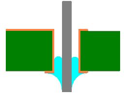
19 Selective Soldering by miniaturized solder waves Heat transfer by flowing solder within a limited area Seite 19


20 Energy transfer into a solder joint with 100% connection to a copper layer ERSA FhG ISIT Massive heat flow into Cu-layer Seite 20


21 Energy transfer into a solder joint with heat trap present ERSA FhG ISIT Reduced heat flow into Cu-layer Seite 21


22 Heat Traps and their Mode of Action on Printed Circuit Boards Heat traps reduce the heat carrying cross section to those copper layers attached to the joining location Retaining the heat energy in the joining location is improved The joining location heats up more quickly Desired Effect Seite 22


23 Heat Traps - Layout recommendations Seite 23
")

24 Insufficient usage of top side heaters When the top side heaters can t transfer sufficient energy to heat up the boards top side, all the energy to heat up the solder joint (PCB + pin) must be transfered from the bottom side of the assembly. To ensure a rapid heat up of the solder joint, thermal support vias transfer a large amount of heat additionally to the PCB top side. Seite 24


25 Heat Traps for Busbars- Layout Recommendations X X Dimension: d 4 X d 2 d 3 X d 1 d 1 d 2 + d 3 + d 4 Please Note: The cross sectional area of the bus bar is reduced by the drillings! Seite 25


26 Layout recommendations Heat traps to reduce the heat flow into a massive copper layer. This layout is recommended for all layers of a PCB. Thermal support vias to improve the transfer of heat up to the PCB top side. Reducing the heat capacity of a busbar. Reducing the diameter lowers the heat flow from the pin into the busbar. Note that for all above layout recommendations, the current density has always to be taken into consideration! Seite 26


27 Layout Capillary Action with Wave- and Selective Soldering Ratio of diameter pin through-hole capillary gap To increase the transfer of heat into the plated through-hole, it is recommended to work on the upper limit of the capillary gap. In power electronics the gap is 0,25 0,30 mm Seite 27
28 Calculating the hole diameter for square pins G A = pin dimension D = A x 2 D G = required for insertion d H = D + (2 x G) A G d H Seite 28
29 Possible Sources of Defects in the Selective Soldering Process Soldering System related Same Error Pattern! Component related Typical Error Pattern in Practice Non-Wetting Insufficient Capillary Rise Bridging Copper Leaching Pad- and/or Fillet Lifting SMDs Desoldered Layout Layout Layout Seite 29
30 Conclusion Selective soldering of thick copper PCBs with mini wave systems is possible. The layout of the PCB plays of crucial role - especially the connection of inner layers to THTs and the ratio of pin to hole diameter. The specification of the PCB laminate has to be adapted to the higher solder temperatures. The delamination temperature T D is especially critical! The more copper layers are in the board, the smaller will be the process window for soldering. Seite 30
31 Conclusion The board layout has a large influence on the capillary rise and the formation of bridges The cause variables in the layout are Pad size / Contact spacing Pin length Plating of PTH joined to copper layers Size of capillary gap Distance between THT and SMD Seite 31
")
")
32 The Process: Flux (F) Preheat (PH) Soldering (S) Seite 32


33 FLUXING METHODS: Drop Jet Fluxer Airless system. Precise Deposition. 2mm Dot Size. Programmable Flux Amounts per joint. No Clean, Water Soluble and Rosin Up to 15% solids. Ultrasonic Fluxer Precise Deposition. Good for Spraying Rows. Good for High Solids Rosin Fluxes. Spray Fluxer Good for use of Chip Wave Style nozzle in selective. Seite 33

34 Preheating: Top and Bottom Seite 34
35 Preheating Multilayer Boards Telecommunication (24 Layers) T T +++ If, for multi-layer assemblies, thermal energy is supplied only from one side (lower side), then the heat has to travel, layer by layer, from the bottom up through the board. Since each layer absorbs energy, a temperature gradient exists from bottom to top of the board. Therefore, to achieve a uniform and homogeneous heating of the board, a correspondingly long time has to be accepted. T Seite 35
!")
36 Preheating: Multi-layer Boards with IR from bottom LP Bottom Side Surface Temperature ΔT 30K LP Top Side Temperature Critical! 160 C Long Preheat Time 140s IR Preheater only from bottom side, with maximum power (100%)! Seite 36
!")
37 Preheating: Multi-layer Boards with IR from bottom LP Bottom Side Surface Temperature LP Top Side Temperature ΔT 20K High! 150 C Very Long Preheat Time 190s IR Preheater only from bottom side, with reduced power (66%)! Seite 37
38 Preheating Multilayer Boards - Telecommunication (24 Layers) T +++ T T +++ If multi-layer boards are supplied with thermal energy from both sides, the heat penetrates the board simultaneously from top and from bottom. As a result, the temperature gradient is very small, and the board warms up uniformly and homogeneously at a much faster rate. At the same time, the stress experienced by the lower side is reduced, and the danger that the flux is damaged during the preheat process is minimized. Seite 38
! LP Top Side Temperature Short Preheat Time 110s Seite 39")
39 Preheating: Multi-layer Board with IR from bottom + convection from top LP Bottom Side Surface Temperature ΔT 10K Not Critical! 140 C Preheating from bottom and from top, with reduced power (65%)! LP Top Side Temperature Short Preheat Time 110s Seite 39
40 Forced Convection Top side pre-heating The use of Multijet Forced Convection Optional Top side pre-heating guarantees a constant PCB temperature during the entire selective soldering process. This guarantees that each solder joint is made under the same thermal conditions. Highly recommended for heavy, multilayer PCBs which require a long process. Seite 40
41 Hole Fill Voiding Cu Dissolution Copper Dissolution and The Need For Preheat Interaction Plot for Voiding Interaction Plot for Cu Dissolution 10 Board Thickness/Surface Finish Board Thickness/Surface Finish =.093" 106AX-HT OSP 2 =.093" ImAg 5 1 =.093" 106AX-HT OSP 2 =.093" ImAg Pot Temperature Pot Temperature = Low Voiding (0% - 5%) 5 = Medium Voiding (5% - 10%) 10 = High Voiding ( >10%) 0 = No Dissolution 5 = Slight Dissolution 10 = Total Dissolution Interaction Plot for Hole Fill = 0% - 25% Hole Fill 5 = 25% - 75% Hole Fill 10 = 75% - 100% Hole Fill Pot Temperature 290 Board Thickness/Surface Finish =.093" 106AX-HT OSP 2 =.093" ImAg The more thermal energy you have in your board, the lower your pot temperature And dwell time can be in order to achieve a Good solder joint. No preheat or not enough Preheat warrants higher pot temps and Higher dwell times in order to topside fill On thermally challenging boards. Seite 41
42 The Soldering Module: Things to Consider. Single Point or Multi-dip Moving Pot or Moving the Board Positional Accuracy of the Gantry Pumping Mechanism for Wave Height Dual Alloy Capable Fidicual Recognition Board Warpage Detection Nozzle Types and Sizes Nozzle Cleaning Keep out Areas Seite 42

43 Multi-dip Single Point XYZ Seite 43


44 Multi-Dip Tooling Pros: Fast Cycle Times Cons: Dedicated Tooling Change Over time Tooling Cost Universal Dwell time for all joints Requires Larger Keep out Area More N2 Consumption with Hood Seite 44
45 Reflowlöten Configuration - Single Solder Nozzle - Constant solder flow over the complete nozzle surface no preferred direction for solder to drain - Continuous heat transfer into the solder joint during the solder process - No orientation of the component to the solder nozzle required - No layout constraints for the orientation of the components - Suitable for a wide variety of solder alloys - Individual Wave Height and Dwell Time per Joint Seite 45

46 Moving the Board or the Pot Seite 46


47 Gripper Systems moves the entire PCB with a gripper system, one PCB at a time. Only Localized top side preheat possible. - moving only the solder pot is 50% faster. - no risk of vibration during cooling. - moving solder pot does not require component fixing. - top side preheating keeps PCB temp. constant during soldering. - a machine with segmented process steps can handle up to 6 PCBs at the same time! Seite 47

48 B A C D A D V A N T A G ES: For soldering the square socket just program a line and move the solder nozzle from A to B B to C C to D D to A and peel off It is not required to either turn the board or the solder nozzle, or to change any angles. A recommended orientation of the components is unnecessary Seite 48
49 Repeatability is Critical Seite 49


 - No adjustment after servicing the solder")
50 Reflowlöten Design of Solder Bath - Maintenance-free design with electro-magnetic solder pump - No mechanical movable part in the solder bath - Precise wave height due to continuous circulation of solder - Outstanding repeatability of solder process (no impeller) - No adjustment after servicing the solder bath Seite 50


51 Reflowlöten Monitoring - Solder Bath - Solder wave height is measured - Solder level in bath is monitored / Solder wire feeder option - Solder temperature is exactly controlled - N2 atmosphere assures stabile process conditions play video click button Seite 51

52 Solder Module Reflowlöten Seite 52


53 Reflowlöten Configuration Solder Module Z - variable Different nozzle geometries Variety of Alloys - Both solder bath can be raised, separately and individually, on the axis up to the required working height (z- direction) - Depiction of mode of operation with two identical nozzles but different alloys. - Depiction of mode of operation with two nozzles of different geometries and identical solder. Seite 53


54 Reflowlöten Configuration Solder Module Y- variable - The distance of solder bath 1 to solder bath 2 can be adjusted on the axis system in the y-direction. - Set-up for simultaneous soldering of two assemblies of a multi-up panel. Seite 54


55 Reflowlöten Solder Snap-Off with Wettable Nozzle Surfaces F1= Wetting Force F2= Capillary Force F3= Gravity F4= Adhesive Forces - Solder snap-off, the point in the process when the solder breaks off from the solder joint, is positively assisted by the adhesive force F4, which is generated by the wettable surface of the nozzle. - This adhesive force, in conjunction with gravity F3, enables the solder to properly drain off from the solder joint after having formed it, and to eliminate bridging and shorts. Seite 55


56 Reflowlöten Solder Snap-Off with Wettable Nozzle Surfaces Standard Snap-Off - forms convex solder joints Controlled Snap-Off - forms concave solder joints Seite 56


57 Reflowlöten Automatic Nozzle Activation: Automatic, preventive activation of the nozzle surface to prevent the surface from dewetting. The uniform wetting of the outer surface of the solder nozzles is essential for a stable process and constant soldering results. By a charging screw adipic powder will be applied on the solder nozzle in a specified interval. Seite 57


58 Fiducial and Board Warpage The need for fiducial Recognition and Board Warp Detection is highly Dependent on the Assembly. Seite 58

59 Min. distance of a single solder point from the adjacent SMD pad or from the conveyor* BE Pad Bohrung Pin Scrap edge 3 mm 3 mm 6 mm Seite 59

60 Off-centre positioning possibility of the solder wave Seite 60


61 Minimum Distance of a multi-row connector to the adjacent SMD Pads* Component Pad Through Hole 1 mm Seite 61
* Blue = Required keep out area A = distance between pads B = distance between pads 1 mm 2 mm This recommendation should be used for")
62 Keep out area around dual and multi row solder joints (pitch 2.54 mm)* Blue = Required keep out area A = distance between pads B = distance between pads 1 mm 2 mm This recommendation should be used for all double and multi row layouts, starting with a pitch of > 2,54 mm. Seite 62


63 keep out areas around selective solder joints No keep out areas or solder thieves required! X Seite 63
64 Programming Methods Joystick Teach : Pro Easy to use Con- VERY Time consuming and Machine is not producing while teaching, Requires live product Offline Programming: Pro Machine runs production while programs created offline, Easy to Use, Auto routing and cycle time calculations, CAD DXF or JPG, Very Accurate! Con- Need Computer Knowledge Data Entry Pro- Can be done while machine is running Con- Requires hand measurements, VERY Time consuming. Seite 64


65 Scale Image Result: Scaled and rotated image Seite 65

66 3D-View of Blocking Zones Visual Monitoring due to 3D-View Seite 66
67 Optimized Line Optimized Cycel Times Seite 67


68 Multi Panel Profils can be easy duplicated Time optimized programming for multi panels Seite 68

69 Parameter-Set Up Selection can be done in the graphic or in the Set-Data-List Seite 69

70 Thank you for your attention!!! We hope we can work with you for your soldering needs. Seite 70
Position Accuracy Machines for Selective Soldering Fine Pitch Components Gerjan Diepstraten Vitronics Soltec B.V. Oosterhout, Netherlands
 As originally published in the IPC APEX EXPO Conference Proceedings. Position Accuracy Machines for Selective Soldering Fine Pitch Components Gerjan Diepstraten Vitronics Soltec B.V. Oosterhout, Netherlands
Effects of an Appropriate PCB Layout and Soldering Nozzle Design on Quality and Cost Structure in Selective Soldering Processes
 Effects of an Appropriate PCB Layout and Soldering Nozzle Design on Quality and Cost Structure in Selective Soldering Processes Reiner Zoch, Product Manager Christian Ott, Sales and Project Manager SEHO
Application Note 5026
 Surface Laminar Circuit (SLC) Ball Grid Array (BGA) Eutectic Surface Mount Assembly Application Note 5026 Introduction This document outlines the design and assembly guidelines for surface laminar circuitry
Assembly Instructions for SCA6x0 and SCA10x0 series
 Technical Note 71 Assembly Instructions for SCA6x0 and SCA10x0 series TABLE OF CONTENTS Table of Contents...1 1 Objective...2 2 VTI'S DIL-8 and DIL-12 packages...2 3 Package Outline and Dimensions...2
"Wave Soldering is in no way a dying art!" Technical article published by "Markt & Technik", issue 6, 02_2012
 Karin Zühlke, Markt & Technik Jürgen Friedrich, Commonly held preconceptions about wave soldering are mostly the result of its highly complex process controls Wave Soldering is in no way a dying art! Ersa,
Assembly Instructions for SCC1XX0 series
 Technical Note 82 Assembly Instructions for SCC1XX0 series TABLE OF CONTENTS Table of Contents...1 1 Objective...2 2 VTI's 32-lead Dual In-line Package (DIL-32)...2 3 DIL-32 Package Outline and Dimensions...2
Application Note 5334
 Soldering and Handling of High Brightness, Through Hole LED Lamps Application Note 5334 Introduction LEDs are well known for their long useful life compared to conventional incandescent bulb. If an LED
Bob Willis Process Guides
 What is a Printed Circuit Board Pad? What is a printed circuit board pad, it may sound like a dumb question but do you stop to think what it really does and how its size is defined and why? A printed circuit
Soldering Methods and Procedures for Vicor Power Modules
 APPLICATION NOTE AN:208 Soldering Methods and Procedures for Vicor Power Modules Lead-Free Pins (RoHS); TIN / LEAD PINS (see page 7) Contents Page Overview 1 Analysis of a Good Solder Joint 1 Soldering
'*+,+$&#' ' '") !"#$%&'()'*"+,+$&#' *";
!"#$%&'()'*"+,+$&#' *"; TOLERANCE FORGOTTEN: IMPACTS OF TODAY S COMPONENT PACKAGING AND COPPER ROUTING ON ELECTRONIC
 TOLERANCE FORGOTTEN: IMPACTS OF TODAY S COMPONENT PACKAGING AND COPPER ROUTING ON ELECTRONIC Presented By: Dale Lee E-mail: Dale.Lee@Plexus.Com April 2013 High Layer Counts Wide Range Of Component Package
Copper Dissolution: Just Say No!
 Korea s New Electronics Waste Law, p. 18 AUGUST 2007 circuitsassembly.com Copper Dissolution: Just Say No! Connector after conventional SAC 305 rework showing copper dissolution (left), and minimal copper
SMT Troubleshooting. Typical SMT Problems For additional process solutions, please refer to the AIM website troubleshooting guide
 SMT Troubleshooting Typical SMT Problems For additional process solutions, please refer to the AIM website troubleshooting guide Solder Balling Solder Beading Bridging Opens Voiding Tombstoning Unmelted
14.8 Designing Boards For BGAs
 exposure. Maintaining proper control of moisture uptake in components is critical to the prevention of "popcorning" of the package body or encapsulation material. BGA components, before shipping, are baked
Prepared by Qian Ouyang. March 2, 2013
 AN075 Rework Process for TQFN Packages Rework Process for TQFN Packages Prepared by Qian Ouyang March 2, 2013 AN075 Rev. 1.1 www.monolithicpower.com 1 ABSTRACT MPS proprietary Thin Quad Flat package No
Chapter 11 Testing, Assembly, and Packaging
 Chapter 11 Testing, Assembly, and Packaging Professor Paul K. Chu Testing The finished wafer is put on a holder and aligned for testing under a microscope Each chip on the wafer is inspected by a multiple-point
Technical Note 1 Recommended Soldering Techniques
 1 Recommended Soldering Techniques Introduction The soldering process is the means by which electronic components are mechanically and electrically connected into the circuit assembly. Adhering to good
Module No. # 07 Lecture No. # 35 Vapour phase soldering BGA soldering and De-soldering Repair SMT failures
 An Introduction to Electronics Systems Packaging Prof. G. V. Mahesh Department of Electronic Systems Engineering Indian Institute of Science, Bangalore Module No. # 07 Lecture No. # 35 Vapour phase soldering
Process Troubleshooting Guide. Selective Soldering Process Manual and Manufacturability Guideline
 Process Troubleshooting Guide Selective Soldering Process Manual and Manufacturability Guideline NOTICE This is a Nordson SELECT publication that is protected by copyright. Original copyright date 2017.
BGA (Ball Grid Array)
") BGA (Ball Grid Array) National Semiconductor Application Note 1126 November 2002 Table of Contents Introduction... 2 Package Overview... 3 PBGA (PLASTIC BGA) CONSTRUCTION... 3 TE-PBGA (THERMALLY ENHANCED
BGA (Ball Grid Array) National Semiconductor Application Note 1126 November 2002 Table of Contents Introduction... 2 Package Overview... 3 PBGA (PLASTIC BGA) CONSTRUCTION... 3 TE-PBGA (THERMALLY ENHANCED
Surface Mount Technology Integration of device connection technology in the SMT process Let s connect. White Paper
 Surface Mount Technology Integration of device connection technology in the SMT process Let s connect White Paper Surface Mount Technology Integration of device connectivity in the SMT process Today's
Initial release of document
 This specification covers the requirements for application of SMT Poke In Connectors for use on printed circuit (pc) board based LED strip lighting typically used for sign lighting. The connector accommodates
!"#$%&'()'*"+,+$&#' ' '
'*+,+$&#' ' '") !"#$%&'()'*"+,+$&#' *"89"+&+6'B22&83%45'8/6&10/%2'A"1'/22&83%4'/+#'C"0+0+D'8&67"#2'0+'&%&
!"#$%&'()'*"+,+$&#' *"89"+&+6'B22&83%45'8/6&10/%2'A"1'/22&83%4'/+#'C"0+0+D'8&67"#2'0+'&%&
Handling and Processing Details for Ceramic LEDs Application Note
 Handling and Processing Details for Ceramic LEDs Application Note Abstract This application note provides information about the recommended handling and processing of ceramic LEDs from OSRAM Opto Semiconductors.
What Can No Longer Be Ignored In Today s Electronic Designs. Presented By: Dale Lee
 What Can No Longer Be Ignored In Today s Electronic Designs Presented By: Dale Lee E-mail: Dale.Lee@Plexus.Com 24 January 2008 Introduction Component packaging technology continues to decrease in size
A review of the challenges and development of. the electronics industry
 SMTA LA/OC Expo, Long Beach, CA, USA A review of the challenges and development of SMT Wave and Rework assembly processes in SMT, the electronics industry Jasbir Bath, Consulting Engineer Christopher Associates
Selective Soldering How it has evolved to become an Integral. Method in Todays Manufacturing Processes
 2187 Selective Soldering How it has evolved to become an Integral Method in Todays Manufacturing Processes Patrick McWiggin, SolderStar s Technical Director Since regulations were bought in from the European
BREAKING THROUGH FLUX RESIDUES TO PROVIDE RELIABLE PROBING ON PCBAS- CONSISTENT CONNECTIONS ACROSS DIFFERENT NO-CLEAN SOLDERS, FLUXES AND LAND DESIGNS
 BREAKING THROUGH FLUX RESIDUES TO PROVIDE RELIABLE PROBING ON PCBAS- CONSISTENT CONNECTIONS ACROSS DIFFERENT NO-CLEAN SOLDERS, FLUXES AND LAND DESIGNS Paul Groome, Ehab Guirguis Digitaltest, Inc. Concord,
Overcoming the Challenges of HDI Design
 ALTIUMLIVE 2018: Overcoming the Challenges of HDI Design Susy Webb Design Science Sr PCB Designer San Diego Oct, 2018 1 Challenges HDI Challenges Building the uvia structures The cost of HDI (types) boards
mcube WLCSP Application Note
 AN-002 Rev.02 mcube WLCSP Application Note AN-002 Rev.02 mcube, Inc. 1 / 20 AN-002 Rev.02 Guidelines for Printed Circuit Board (PCB) Design and Assembly with mcube Wafer Level Chip Scale Package (WLCSP)
BGA inspection and rework with HR 600/2 Failure analysis and assembly repair
 Even today some assemblies including BGA components still show soldering failures that require as a consequence to rework the BGA. The following example can be seen as a typical case for today s inspection
Improve SMT Assembly Yields Using Root Cause Analysis in Stencil Design
 Improve SMT Assembly Yields Using Root Cause Analysis in Stencil Design Greg Smith FCT Assembly, Inc. gsmith@fctassembly.com This paper and presentation was first presented at the 2017 IPC Apex Expo Technical
Application Note. Soldering Guidelines for Surface Mount Filters. 1. Introduction. 2. General
 Soldering Guidelines for Surface Mount Filters 1. Introduction This Application Guideline is intended to provide general recommendations for handling, mounting and soldering of Surface Mount Filters. These
CHAPTER 11: Testing, Assembly, and Packaging
 Chapter 11 1 CHAPTER 11: Testing, Assembly, and Packaging The previous chapters focus on the fabrication of devices in silicon or the frontend technology. Hundreds of chips can be built on a single wafer,
M series. Product information. Koki no-clean LEAD FREE solder paste. Contents. Lead free SOLUTIONS you can TRUST.
 www.ko-ki.co.jp Ver. 42017e.2 Prepared on Oct. 26, 2007 Koki no-clean LEAD FREE solder paste Anti-Pillow Defect Product information This Product Information contains product performance assessed strictly
FPC connectors (0.3mm pitch) Front lock with FPC tabs
 Front lock with FPC tabs") AYF31 For FPC FPC connectors (0.3mm pitch) Front lock with FPC tabs Y3FT Series FEATURES 1. Low-profile, space-saving design (pitch: 0.3mm) The 0.9mm height, 3.0mm depth contributes to the miniaturization
AYF31 For FPC FPC connectors (0.3mm pitch) Front lock with FPC tabs Y3FT Series FEATURES 1. Low-profile, space-saving design (pitch: 0.3mm) The 0.9mm height, 3.0mm depth contributes to the miniaturization
Study on Solder Joint Reliability of Fine Pitch CSP
 As originally published in the IPC APEX EXPO Conference Proceedings. Study on Solder Joint Reliability of Fine Pitch CSP Yong (Hill) Liang, Hank Mao, YongGang Yan, Jindong (King) Lee. AEG, Flextronics
Application Note AN-1011
 AN-1011 Board Mounting Application Note for 0.800mm Pitch Devices For part numbers IRF6100, IRF6100PBF, IR130CSP, IR130CSPPBF, IR140CSP, IR140CSPPBF, IR1H40CSP, IR1H40CSPPBF By Hazel Schofield and Philip
For FPC. FPC connectors (0.2mm pitch) Back lock
 Back lock") 0.9 For FPC FPC connectors (0.2mm pitch) Back lock Y2B Series AYF21 New FEATURES 1. Slim and low profile design (Pitch: 0.2 mm) 0.2 mm pitch back lock design and the slim body with a 3.15 mm depth (with
0.9 For FPC FPC connectors (0.2mm pitch) Back lock Y2B Series AYF21 New FEATURES 1. Slim and low profile design (Pitch: 0.2 mm) 0.2 mm pitch back lock design and the slim body with a 3.15 mm depth (with
AN5046 Application note
 Application note Printed circuit board assembly recommendations for STMicroelectronics PowerFLAT packages Introduction The PowerFLAT package (5x6) was created to allow a larger die to fit in a standard
For board-to-fpc. Narrow pitch connectors (0.4mm pitch)
") Automation Controls Catalog For board-to-fpc Narrow pitch connectors (0.4mm pitch) F4 Series 5.0mm 4.1mm RoHS compliant FEATURES 1. 0.9 mm mated height low profile two-piece type connectors 2. Strong resistance
Automation Controls Catalog For board-to-fpc Narrow pitch connectors (0.4mm pitch) F4 Series 5.0mm 4.1mm RoHS compliant FEATURES 1. 0.9 mm mated height low profile two-piece type connectors 2. Strong resistance
Is Now Part of To learn more about ON Semiconductor, please visit our website at
 Is Now Part of To learn more about ON Semiconductor, please visit our website at www.onsemi.com ON Semiconductor and the ON Semiconductor logo are trademarks of Semiconductor Components Industries, LLC
AN-5067 PCB Land Pattern Design and Surface Mount Guidelines for MLP Packages
 Introduction AN-5067 Fairchild Semiconductor Application Note September 2005 Revised September 2005 PCB Land Pattern Design and Surface Mount Guidelines for MLP Packages The current miniaturization trend
Our Top 10 Commonly Asked Soldering Questions This Year
 Our Top 10 Commonly Asked Soldering Questions This Year 1 Chip Component Shifting Can be related to components floating on the molten solder plus the equipment may have vibrations, which may not be felt
For FPC. FPC connectors (0.3mm pitch) Back lock
 Back lock") 0.9 For FPC FPC connectors (0.3mm pitch) Back lock AYF33 Y3B/Y3BW Series New Y3B Y3BW is added. FEATURES 1. Slim and low profile design (Pitch: 0.3 mm) Back lock type and the slim body with a 3.15 mm depth
0.9 For FPC FPC connectors (0.3mm pitch) Back lock AYF33 Y3B/Y3BW Series New Y3B Y3BW is added. FEATURES 1. Slim and low profile design (Pitch: 0.3 mm) Back lock type and the slim body with a 3.15 mm depth
mcube LGA Package Application Note
 AN-001 Rev.02 mcube LGA Package Application Note AN-001 Rev.02 mcube, Inc. 1 / 21 AN-001 Rev.02 Guidelines for Printed Circuit Board (PCB) Design and Assembly with mcube Land Grid Array (LGA) Package Sensors
ELS 3.3 Inline selective soldering system
 L Ö T T E C H N I K ELS 3.3 Inline selective soldering system Multi-axis soldering systems for flexible production with a high level of product mix The Inertec ELS 3.3 Inline is the best solution for flexible
Inspection Method Sheet
 Inspection Method Sheet Part Number: Generic Part Name: PCB Filters Drawing Number: Generic Operation: In Process / Final Page 1 of 10 Written By: Myra Cope Doc. #: TT-PC-0378 Rev. 14 Date: 10-15-08 Applicable
Fill the Void IV: Elimination of Inter-Via Voiding
 Fill the Void IV: Elimination of Inter-Via Voiding Tony Lentz FCT Assembly Greeley, CO, USA Greg Smith BlueRing Stencils Lumberton, NJ, USA ABSTRACT Voids are a plague to our electronics and must be eliminated!
Application Specification Releasable Poke-in Connector 08JUL 2015 REV:A
 Application Specification 114-137055 Releasable Poke-in Connector 08JUL 2015 REV:A 1. INTRODUCTION This specification covers the requirements for application of Releasable Poke-in connector for use on
Lead Forming. Automatic Selective Soldering Systems. Since more than 25 years the cutting and forming of THT components is the core business of EBSO.
 Lead Forming Since more than 25 years the cutting and forming of THT components is the core business of EBSO. With over 20 standard preforming machines we can provide solutions to any kind of lead forming
An Introduction to Electronics Systems Packaging. Prof. G. V. Mahesh. Department of Electronic Systems Engineering
 An Introduction to Electronics Systems Packaging Prof. G. V. Mahesh Department of Electronic Systems Engineering Indian Institute of Science, Bangalore Module No. # 07 Lecture No. # 33 Reflow and Wave
APPLICATION SPECIFICATION LEAD FREE REFLOW PROFILE FOR SMD S AND WAVE SOLDERED (MODULAR TELEPHONE JACK S)
") APPLIATION SPEIFIATION LEAD FREE REFLOW PROFILE FOR SMD S AND WAVE SOLDERED (MODULAR TELEPHONE JAK S) 1.0 SOPE The purpose of this document is to outline the application of the surface mounted and true
APPLIATION SPEIFIATION LEAD FREE REFLOW PROFILE FOR SMD S AND WAVE SOLDERED (MODULAR TELEPHONE JAK S) 1.0 SOPE The purpose of this document is to outline the application of the surface mounted and true
Reflow soldering guidelines for surface mounted power modules
 Design Note 017 Reflow soldering guidelines for surface mounted power modules Introduction Ericsson surface mounted power modules are adapted to the ever-increasing demands of high manufacturability and
LED Mounting Techniques
 LED Mounting Techniques Contents 1. Introduction 2. Solder Paste Printing 3. LED Placement 4. Reflow Soldering 5. Verification of LED Mounting Performance 6. Others 7. Request 1/13 LED Mounting Techniques
How to solder SMD component on Awesome PCB or any other kind of PCB.
 How to solder SMD component on Awesome PCB or any other kind of PCB. Step by step tutorial, with no steps to skip. Step 1 - What do we need? Step 2 - Fixing PCB Step 3 - Preparing for soldering Step 4
Application Note. Soldering Guidelines for Module PCB Mounting Rev 13
 Application Note Soldering Guidelines for Module PCB Mounting Rev 13 OBJECTIVE The objective of this application note is to provide ANADIGICS customers general guidelines for PCB second level interconnect
DVD-PTH-C Through-Hole Solder Joint Workmanship Standards
 DVD-PTH-C Through-Hole Solder Joint Workmanship Standards Below is a copy of the narration for the DVD-PTH-C video presentation. The contents for this script were developed by a review group of industry
Is Now Part of To learn more about ON Semiconductor, please visit our website at
 Is Now Part of To learn more about ON Semiconductor, please visit our website at www.onsemi.com ON Semiconductor and the ON Semiconductor logo are trademarks of Semiconductor Components Industries, LLC
Application Note. Soldering Guidelines for SMPS Multilayer Ceramic Capacitor Assemblies
 Application Note AN37-0012 Soldering Guidelines for SMPS Multilayer Ceramic Capacitor Assemblies 1. Introduction With a very low ESR and ESL and the ability to withstand very high levels of di/dt and dv/dt,
To See is to Survive!
 INSPECTION SYSTEMS for the 21 s t Century To See is to Survive! In todayõs highly competitive manufacturing environment, the ability to see and react to hidden production deficiencies, in order to guarantee
Surface Mount Connectors
 Surface Mount Connectors 3 As the industry s first surfacemountable connectors to be supplied on a continuous reel, our surface mount connectors are designed to be used as part of Zierick s Surf-Shooter
Solder Fillets of Surface Mounted Connectors
 Workmanship Specification 101-21 25May07 Rev B 1. SCOPE Solder Fillets of Surface Mounted Connectors This specification covers the acceptable requirements and the not acceptable conditions for the solder
FPC CONNECTORS Y3FT (0.3 mm pitch) with FPC tabs
 with FPC tabs") AYF31 FPC CONNECTORS FOR FPC CONNECTION FPC CONNECTORS Y3FT (0.3 mm pitch) with FPC tabs (Former Name: YF31) FEATURES 1. Low-profile, space-saving design (pitch: 0.3mm) The 0.9mm height, 3.0mm depth contributes
AYF31 FPC CONNECTORS FOR FPC CONNECTION FPC CONNECTORS Y3FT (0.3 mm pitch) with FPC tabs (Former Name: YF31) FEATURES 1. Low-profile, space-saving design (pitch: 0.3mm) The 0.9mm height, 3.0mm depth contributes
TECHNICAL INFORMATION
 TECHNICAL INFORMATION Super Low Void Solder Paste SE/SS/SSA48-M956-2 [ Contents ] 1. FEATURES...2 2. SPECIFICATIONS...2 3. VISCOSITY VARIATION IN CONTINUAL PRINTING...3 4. PRINTABILITY..............4 5.
CF Series AXC5/AXC6. FEATURES 1. Vertical mating type with a 0.8 mm mated height low profile design
 For board-to-micro coaxial wire Micro coaxial connectors (Low profile) AC5/AC6 CF Series 2. with strong resistance to various environments provides high contact reliability and facilitates connection work
Bumping of Silicon Wafers using Enclosed Printhead
 Bumping of Silicon Wafers using Enclosed Printhead By James H. Adriance Universal Instruments Corp. SMT Laboratory By Mark A. Whitmore DEK Screen Printers Advanced Technologies Introduction The technology
Improve SMT Assembly Yields Using Root Cause Analysis in Stencil Design
 Improve SMT Assembly Yields Using Root Cause Analysis in Stencil Design Greg Smith FCT Assembly, Inc. Greeley, CO Abstract Reduction of first pass defects in the SMT assembly process minimizes cost, assembly
S3X58-M High Reliability Lead Free Solder Paste. Technical Information. Koki no-clean LEAD FREE solder paste.
 www.ko-ki.co.jp #52007 Revised on Nov.27, 2014 Koki no-clean LEAD FREE solder paste High Reliability Lead Free Solder Paste S3X58-M500-4 Technical Information O₂ Reflowed 0.5mmP QFP 0603R This product
DEPARTMENT OF DEFENSE TEST METHOD STANDARD METHOD 210, RESISTANCE TO SOLDERING HEAT
 INCH-POUND MIL-STD-202-210 18 April 2015 SUPERSEDING MIL-STD-202G w/change 2 (IN PART) 28 June 2013 (see 6.1) DEPARTMENT OF DEFENSE TEST METHOD STANDARD METHOD 210, RESISTANCE TO SOLDERING HEAT AMSC N/A
Surface Mount Header Assembly Employs Capillary Action
 New Product Technology Surface Mount Header Assembly Employs Capillary Action Zierick s unique header assembly features capillary action to improve solder joint strength. As a result, pin retention force
For board-to-fpc. Narrow pitch connectors (0.4mm pitch)
") Automation Controls Catalog For board-to-fpc Narrow pitch connectors (0.4mm pitch) A4F Series 3.0mm 2.4mm RoHS compliant FEATURES 1. 0.6 mm mated height low profile two-piece type connector 2. Space-saving
Automation Controls Catalog For board-to-fpc Narrow pitch connectors (0.4mm pitch) A4F Series 3.0mm 2.4mm RoHS compliant FEATURES 1. 0.6 mm mated height low profile two-piece type connector 2. Space-saving
Handling and Processing Details for Ceramic LEDs Application Note
 Handling and Processing Details for Ceramic LEDs Application Note Abstract This application note provides information about the recommended handling and processing of ceramic LEDs from OSRAM Opto Semiconductors.
Plated Through Hole Fill:
 Welcome to the EPTAC Webinar Series: Plated Through Hole Fill: Understanding the Process and Assembly Requirements You are connected to our live presentation delivered via the internet. The webinar will
AltiumLive 2017: Creating Documentation for Successful PCB Manufacturing
 AltiumLive 2017: Creating Documentation for Successful PCB Manufacturing Julie Ellis TTM Field Applications Engineer Thomas Schneider Field Applications Engineer 1 Agenda 1 Complexity & Cost 2 3 4 5 6
BOARD DESIGN, SURFACE MOUNT ASSEMBLY AND BOARD LEVEL RELIABILITY ASPECTS OF FUSIONQUAD TM PACKAGES
 BOARD DESIGN, SURFACE MOUNT ASSEMBLY AND BOARD LEVEL RELIABILITY ASPECTS OF FUSIONQUAD TM PACKAGES Ahmer Syed 1, Sundar Sethuraman 2, WonJoon Kang 1, Gary Hamming 1, YeonHo Choi 1 1 Amkor Technology, Inc.
HOTBAR REFLOW SOLDERING
 HOTBAR REFLOW SOLDERING Content 1. Hotbar Reflow Soldering Introduction 2. Application Types 3. Process Descriptions > Flex to PCB > Wire to PCB 4. Design Guidelines 5. Equipment 6. Troubleshooting Guide
Transition to Lead Free Electronics Assembly Case Study Part II Product Reliability and Forced Rework
 Transition to Lead Free Electronics Assembly Case Study Part II Product Reliability and Forced Rework Robert Farrell, Scott Mazur, and Paul Bodmer Benchmark Electronics, Hudson NH Richard Russo, Mercury
The Pin-in-Paste (or AART) Process for Odd Form and Through Hole Printed Circuit Boards
 Process for Odd Form and Through Hole Printed Circuit Boards") The Pin-in-Paste (or AART) Process for Odd Form and Through Hole Printed Circuit Boards Jay B. Hinerman 1, K. Srihari 2, Ph.D. & George R. Westby 3 1 DEK Inc 8 Bartles Corner Road, Flemington, New Jersey
The Pin-in-Paste (or AART) Process for Odd Form and Through Hole Printed Circuit Boards Jay B. Hinerman 1, K. Srihari 2, Ph.D. & George R. Westby 3 1 DEK Inc 8 Bartles Corner Road, Flemington, New Jersey
SNT Package User's Guide
 (Small outline Non-leaded Thin package) [Target Packages] SNT-4A SNT-6A SNT-6A (H) SNT-8A SNT Package User s Guide Introduction This manual describes the features, dimensions, mountability, reliability,
Assembly Guidelines Sterling Silver & MacStan Immersion Tin Coated PCB s
 Assembly Guidelines Sterling Silver & MacStan Immersion Tin Coated PCB s By: MacDermind Final Finish Team MacDermid Inc. Flat solderable surface finishes are required for the increasingly dense PCB designs.
Interposer MATED HEIGHT
 Product Specification: FEATURES High Performance PCBeam Connector Technology Product options at 1.27mm, 1.0mm, and 0.8mm pitch Maximized pin count per form factor 3 form factor sizes available Standard
PAGE 1/6 ISSUE Jul SERIES Micro-SPDT PART NUMBER R516 XXX 10X R 516 _ 1 0 _
 PAGE 1/6 ISSUE Jul-24-2017 SERIES Micro-SPDT PART NUMBER R516 XXX 10X R516 series: the RAMSES concept merges with the SLIM LINE technology, breaking up the frequency limits of SMT switches : - FULL SMT
HSNT Package User's Guide
 CMOS IC Application Note HSNT Package User's Guide ABLIC Inc., 2011-2014 This manual describes the features, package dimensions, recommended land, handling methods as well as marking specifications and
A range of techniques has been devised to quantify the amount of misregistration present in a laminated panel:
 Controlling Multilayer Registration Jim Dermody Operations Technology, Inc. T H E P R 0 B L E M How does one optimize the multilayer fabrication process for best registration of layers and drill patterns?
Data Sheet. HLMP-Yxxx. T-1 (3 mm) GaP/GaAsP LED Lamps. Description. Features. Applications. Package Dimension
 GaP/GaAsP LED Lamps. Description. Features. Applications. Package Dimension") HLMP-Yxxx T-1 (3 mm) GaP/GaAsP LED Lamps Data Sheet Description This family of T-1 lamps is widely used in general purpose indicator and back lighting applications. The optical design is balanced to yield
HLMP-Yxxx T-1 (3 mm) GaP/GaAsP LED Lamps Data Sheet Description This family of T-1 lamps is widely used in general purpose indicator and back lighting applications. The optical design is balanced to yield
CeraDiodes. Soldering directions. Date: July 2014
 CeraDiodes Soldering directions Date: July 2014 EPCOS AG 2014. Reproduction, publication and dissemination of this publication, enclosures hereto and the information contained therein without EPCOS' prior
For FPC. FPC connectors (0.3mm pitch) Back lock
 Back lock") Automation Controls Catalog For FPC FPC connectors (0.3mm pitch) Back lock Y3BL Series New FEATURES 1. Slim and low profile design (Pitch: 0.3 mm) The Y3BL is a 0.6 mm low-profile connector with a back-lock
Automation Controls Catalog For FPC FPC connectors (0.3mm pitch) Back lock Y3BL Series New FEATURES 1. Slim and low profile design (Pitch: 0.3 mm) The Y3BL is a 0.6 mm low-profile connector with a back-lock
Selective Soldering for Interconnection Technology Used in Enterprise Communication Apparatuses
 Selective Soldering for Interconnection Technology Used in Enterprise Communication Apparatuses Mark Woolley, Wesley Brown, and Dr. Jae Choi Avaya Inc. 1300 W 120 th Avenue Westminster, CO 80234 Abstract:
What the Designer needs to know
 White Paper on soldering QFN packages to electronic assemblies. Brian J. Leach VP of Sales and Marketing AccuSpec Electronics, LLC Defect free QFN Assembly What the Designer needs to know QFN Description:
Product Specification - LPS Connector Series
 LPS Product Specification - LPS OVERVIEW The LPS products are solderable versions of those in the Neoconix LPM product series. Also developed for mobile devices and other space-constrained applications,
Product Specification - LPM Connector Family
 LPM Product Specification - LPM OVERVIEW Developed for mobile devices and other space-constrained applications, the Neoconix LPM line of connectors feature exceptional X-Y-Z density with a simple, highly
Application Specification Slim WtoB Poke-in Connector
 Application Specification 114-137049 Slim WtoB Poke-in Connector 18APR 2016 REV:B 1. INTRODUCTION This specification covers the requirements for application of Slim WtoB Poke in connector for use on lighting
RAY S REWORK SECRETS TRAINING CERTIFICATION TEST (DVD-13C) v.3
 v.3") This test consists of twenty multiple-choice questions. All questions are from the video: Ray s Rework Secrets (DVD-13C). Each question has only one most correct answer. Circle the letter corresponding
This test consists of twenty multiple-choice questions. All questions are from the video: Ray s Rework Secrets (DVD-13C). Each question has only one most correct answer. Circle the letter corresponding
Application Specification Ultraminiature Bare Poke-in Contact 26FEB2019 REV:A2
 Application Specification 114-137190 Ultraminiature Bare Poke-in Contact 26FEB2019 REV:A2 1. INTRODUCTION This specification covers the requirements for application of ultraminiature bare poke-in contacts
PAGE 1/6 ISSUE SERIES Micro-SPDT PART NUMBER R516 XXX 10X. (All dimensions are in mm [inches]) R 516 _ 1 0 _
![PAGE 1/6 ISSUE SERIES Micro-SPDT PART NUMBER R516 XXX 10X. (All dimensions are in mm [inches]) R 516 _ 1 0 _](/thumbs/96/127769340.jpg "PAGE 1/6 ISSUE SERIES Micro-SPDT PART NUMBER R516 XXX 10X. (All dimensions are in mm [inches]) R 516 _ 1 0 _") PAGE 1/6 ISSUE 15-10-18 SERIES Micro-SPDT PART NUMBER R516 XXX 10X R516 series: the RAMSES concept merges with the SLIM LINE technology, breaking up the frequency limits of SMT switches : - FULL SMT TECHNOLOGY
PAGE 1/6 ISSUE 15-10-18 SERIES Micro-SPDT PART NUMBER R516 XXX 10X R516 series: the RAMSES concept merges with the SLIM LINE technology, breaking up the frequency limits of SMT switches : - FULL SMT TECHNOLOGY
An Investigation into Lead-Free Low Silver Cored Solder Wire for Electronics Manufacturing Applications
 An Investigation into Lead-Free Low Silver Cored Solder Wire for Electronics Manufacturing Applications Shantanu Joshi 1, Jasbir Bath 1, Kimiaki Mori 2, Kazuhiro Yukikata 2, Roberto Garcia 1, Takeshi Shirai
attocube systems Probe Stations for Extreme Environments CRYOGENIC PROBE STATION fundamentals principles of cryogenic probe stations
 PAGE 88 & 2008 2007 PRODUCT CATALOG CRYOGENIC PROBE STATION fundamentals...................... 90 principles of cryogenic probe stations attocps I.......................... 92 ultra stable cryogenic probe
An introduction to surface mounting
 Data Pack H Issued March 1997 232-5569 An introduction to surface mounting What is surface mounting? In conventional board assembly technology the component leads are inserted into holes through the and
Contact Material Division Business Unit Assembly Materials
 Contact Material Division Business Unit Assembly Materials MICROBOND SOP 91121 P SAC305-89 M3 C Seite 1 Print Performance Soldering Performance General Information MICROBOND SOP 91121 P SAC305-89 M3 Technical