IDeAL program : DSA activity at LETI. S. Tedesco R. Tiron L. Pain
|
|
|
- Jesse Bryan
- 5 years ago
- Views:
Transcription
1 IDeAL program : DSA activity at LETI S. Tedesco R. Tiron L. Pain
2 Outline Why DSA for microelectronics The IDeAL progam Graphoepitaxy of BCP Contact hole application 300 mm pilot line in LETI Conclusion 2
3 Why DSA for Microelectronics? Block copolymers self assembly capabilities Very high resolution Low intrinsic Line Edge Roughness Easy process Low cost C MOS Lithography constraints Control the domain orientations (1D 2D) Alignment control with respect to a preview level Integration capabilities Low defectivity Respect of design rules 3


4 Why DSA for Microelectronics? Advanced lithography SPIE conferences universities industry and large labs of papers on DSA nb DSA a complementary lithography techniques that could get inserted as early as the 14nm node 4
5 Outline Why DSA for microelectronics The IDeAL progam Graphoepitaxy of BCP Contact hole application 300 mm pilot line in LETI Conclusion 5


6 LETI DSA open program Insertion of Directed self Assembly Lithography 6
7 Directed Self Assembly : the lithography? Objectives A new open program to develop a full DSA solution Joint work in LETI environment on material, processes, demonstration & integration A cluster open to materials and equipments suppliers, IDM, EDA Partnership status July 2012 DSA material development Copolymer material worldwide leader : Collaboration with academic laboratories resist partners : under progress Equipment suppliers 2 industrial i partners End users Bilateral work with 7


 Annual Capex : 293 M 80")

8 Arkema in a few points Worldwide player in specialties chemistry Ranging from 1st to 3rd position in product lines insuring 80% of the company revenue revenue : 5,9 Md R&D : > 120M / 8 R&D center WW (US, Japan, France) Annual Capex : 293 M 80 industrial sites employees ARKEMA strength : Worldwide polymer manufacturer Strong know how on block copolymer Ability to quickly ramp up from R&D to industrial scale 8


9 missions? Push material platforms to maturity From lab scale to industry Evaluate advanced copolymer platform Develop 300mm patterning solutions Certify material compatibility with clean room standard Screen DSA material performances Verify transfer capabilities Scale up DSA processes to production level Compatibility with design rules Respect of ITRS standard : defectivity, throughput 9
10 How to go from R&D to industrial? A production oriented consortium DSA Materials Integration Scale e-up mater rial qualific cation Industrial scalability Pre-industrial reactor Lab. scale 300 mm INTEGRATION Defectivity Design compatibility Process development First 300 mm demonstration Process development Etch, Strip, Samples: Process capability Material compatibility Throughput Material properties Patterning capability Maturity III Maturit ty II Maturity I Industr rialization 10


11 ARKEMA LETI partnership : materials path Efficient neutralization layer Several materials under screening PS PMMA platform High platform CD 15nm CD 15nm CD = 7nm CD = 7nm 200 nm 200 nm PS-b-PMMA BCP 100 nm 200 nm High BCP 11
12 Outline Why DSA for microelectronics The IDeAL progam Graphoepitaxy of BCP Contact hole application 300 mm pilot line in LETI Conclusion 12

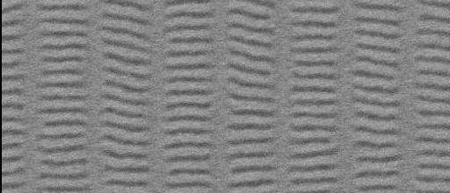
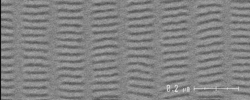

13 Why grapho epitaxy preference? A versatile process LETI demonstration Graphoepitaxy 193nm PCAR HSQ e-beam resist Leti approach 193nm PCAR 193nm NTD Contact shrink 13


14 How to find optimum guiding litho process? => Influence of Litho1 design rules & BCP material A B 200 nm C a 0 Design rule compatibility Optimization of block copolymer selfassembly through graphoepitaxy: A defectivity study R.Tiron et al., JVST B29 06F206 (2011) 200 nm 14


15 Zero Defect Configuration Before litho1 optimization 500 nm After litho1 optimization 500 nm Defectivity measurement enables lithography and process optimization 15


")

 2 /O 2")


16 Silicon Etching with Copolymer Lithography Initial mask (PS) 30 to 100 nm thick SiO 2 Mask (10 nm) Si Si Brush opening (Ar/O 2 plasma) PS plasma treatment Si Si Silicon etching Mask etching (HBr/Cl (CF 4 based plasma) 2 /O 2 plasma) etching on graphoepitaxy Copolymer etching process fully compatible with CMOS requirements Self-assembly patterning using block copolymer for advanced CMOS technology: optimisation of plasma etching process Thierry Chevolleau, CNRS (France)- Paper , SPIE
17 Silicon Etching with Copolymer Lithography Transfer of BCP into Si by using Transfer of BCP into 193 nm SiO2 hard mask trilayer 50 nm Copolymer etching process fully compatible with CMOS requirements 17
18 Outline Why DSA for microelectronics The IDeAL progam Graphoepitaxy of BCP Contact hole application 300 mm pilot line in LETI Conclusion 18
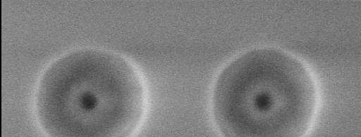
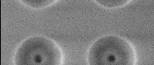
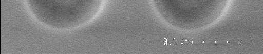
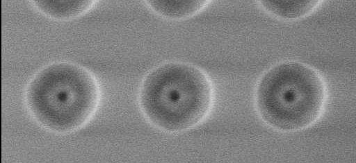
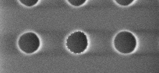
19 Contact shrink and multiplication using DSA of BCP After 193nm litho. After BCP DSA After BCP etching thi Contact Shrink 100 nm Contact Multiplication 100 nm Integration (litho+etch) demonstrated for contact shrink and multiplication 19


20 How to define design rules: Example of code Design Calculated CH placement BF BD SZ0 BF BD+2% SZ+0.5 BF BD-2% SZ-0.5 Simulation contour Contour variation w.r.t. dose, focus and mask CD error variations Experimental validation 53nm + Extracted Contour + Calculated CH position CH position on wafer 20
21 Outline Why DSA for microelectronics The IDeAL progam Graphoepitaxy of BCP Contact hole application 300 mm pilot line in LETI Conclusion 21


 -")
22 DSA 300 mm infrastructure on SOKUDO RF 3 track Process steps Guided litho PS r PMMA spin coat. Grafting Rinse Copolymer coating Self assembly Etching CMOS requirements h freezing neutralization Self assembly Resist hardness to bake and solvent metal/ ionic contamination solvent compatibility Bake time and temp. solvent compatibility metal/ ionic contamination solvent compatibility Throughput Defectivity Transfer capabilities Front end production 300mm track & scanner Pattern density multiplication by direct self-assembly of block copolymers: toward 300mm CMOS requirements Raluca Tiron et al, CEA-Leti (France) - Paper , SPIE


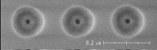
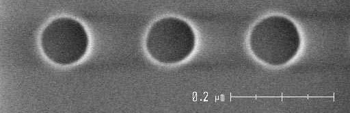
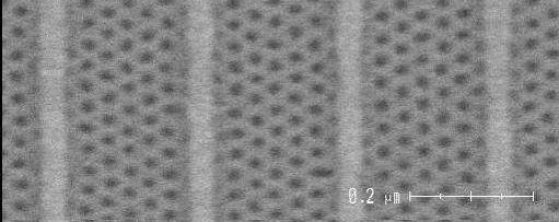
23 Shrink of contact holes 300mm process graphoepitaxy with standard lithography 193nm SiARC SOC SiARC SOC BCP Si CD ~ 100nm 0.2µm CD ~ 15nm 0.2µm 23


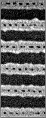
24 Shrink of contact holes 300mm process north west center east south 0.5µm 24
25 Outline Why DSA for microelectronics The IDeAL progam Graphoepitaxy of BCP Contact hole application 300 mm pilot line in LETI Conclusion 25
26 To conclude DSA a complementary lithography technique that could get inserted as early as the 14nm node In a firs step by using PS b PMMA like materials Inasecondstepbyusinghigh materials A realistic application: contact hole shrink and doubling Defectivity is key Thanks for SOKUDO involvement and support 26


27 All this is possible thanks to: A.Gharbi, P.Pimenta-Baross, J. Dubray, S.Barnola, J.Belledent, S.Moulis, R.Tiron LETI X.Chevalier, M.Argoud, C.Navarro Arkema G.Cunge, M.Delalande, T.Chevolleau LTM GFl G.Fleury, G.Hadziioannou, GH LCPO But also LP L.Pain, IC I.Cayrefourcq and dleti peoples involved in the project 27
Status and Challenges for Multibeam DW lithography. L. PAIN CEA - LETI Silicon Technology Department
 Status and Challenges for Multibeam DW lithography L. PAIN CEA - LETI Silicon Technology Department Outline Introduction Challenges Current program status KLA-TENCOR MAPPER Demonstration capability IMAGINE
IMAGINE: an open consortium to boost maskless lithography take off First assessment results on MAPPER technology
 IMAGINE: an open consortium to boost maskless lithography take off First assessment results on MAPPER technology L. Pain (1), B. Icard (1), M. Martin (1), C. Constancias (1), S. Tedesco (1), P. Wiedeman
DSA and 193 immersion lithography
 NIKON RESEARCH CORP. OF AMERICA DSA and 193 immersion lithography Steve Renwick Senior Research Scientist, Imaging Sol ns Technology Development Where the industry wants to go 2 Where we are now 193i e-beam
MAPPER: High throughput Maskless Lithography
 MAPPER: High throughput Maskless Lithography Marco Wieland CEA- Leti Alterative Lithography workshop 1 Today s agenda Introduction Applications Qualification of on-tool metrology by in-resist metrology
Role of mask on the contact etching for 14nm nodes
 Role of mask on the contact etching for 14nm nodes MEBARKI Mokrane 1,2,3 Maxime Darnon 2, Cecile Jenny 1, Nicolas Posseme 3, Delia Ristoiu 1,Germain Servanton 1, Olivier Joubert 2 1 ST Microelectronics
Shooting for the 22nm Lithography Goal with the. Coat/Develop Track. SOKUDO Lithography Breakfast Forum 2010 July 14 (L1)
") Shooting for the 22nm Lithography Goal with the Coat/Develop Track SOKUDO Lithography Breakfast Forum 2010 July 14 (L1) Three (3) different exposure options for 22nm: Public External (L1) MAPPER Lithography
Shooting for the 22nm Lithography Goal with the Coat/Develop Track SOKUDO Lithography Breakfast Forum 2010 July 14 (L1) Three (3) different exposure options for 22nm: Public External (L1) MAPPER Lithography
450mm patterning out of darkness Backend Process Exposure Tool SOKUDO Lithography Breakfast Forum July 10, 2013 Doug Shelton Canon USA Inc.
 450mm patterning out of darkness Backend Process Exposure Tool SOKUDO Lithography Breakfast Forum 2013 July 10, 2013 Doug Shelton Canon USA Inc. Introduction Half Pitch [nm] 2013 2014 2015 2016 2017 2018
Lithography Roadmap. without immersion lithography. Node Half pitch. 248nm. 193nm. 157nm EUVL. 3-year cycle: 2-year cycle: imec 2005
 Lithography Roadmap without immersion lithography Node Half pitch 180 nm 130 nm 90 nm 65 nm 45 nm 32 nm 22 nm 250 nm 180 nm 130 nm 90 nm 65 nm 45 nm 32 nm 248nm 193nm 157nm EUVL 3-year cycle: 2-year cycle:
EUVL Challenges for Next Generation Devices
 EUVL Challenges for Next Generation Devices Center for Semiconductor Research & Development Advanced Lithography Process Technology Dept. Tatsuhiko Higashiki Contents Device Roadmap and Lithography Extendibility
Imec pushes the limits of EUV lithography single exposure for future logic and memory
 Edition March 2018 Semiconductor technology & processing Imec pushes the limits of EUV lithography single exposure for future logic and memory Imec has made considerable progress towards enabling extreme
450mm and Moore s Law Advanced Packaging Challenges and the Impact of 3D
 450mm and Moore s Law Advanced Packaging Challenges and the Impact of 3D Doug Anberg VP, Technical Marketing Ultratech SOKUDO Lithography Breakfast Forum July 10, 2013 Agenda Next Generation Technology
(Complementary E-Beam Lithography)
") Extending Optical Lithography with C E B L (Complementary E-Beam Lithography) July 13, 2011 4008 Burton Drive, Santa Clara, CA 95054 Outline Complementary Lithography E-Beam Complements Optical Multibeam
Extending Optical Lithography with C E B L (Complementary E-Beam Lithography) July 13, 2011 4008 Burton Drive, Santa Clara, CA 95054 Outline Complementary Lithography E-Beam Complements Optical Multibeam
Development of Nanoimprint Mold Using JBX-9300FS
 Development of Nanoimprint Mold Using JBX-9300FS Morihisa Hoga, Mikio Ishikawa, Naoko Kuwahara Tadahiko Takikawa and Shiho Sasaki Dai Nippon Printing Co., Ltd Research & Development Center Electronic Device
Results of Proof-of-Concept 50keV electron multi-beam Mask Exposure Tool (emet POC)
") Results of Proof-of-Concept 50keV electron multi-beam Mask Exposure Tool (emet POC) Elmar Platzgummer *, Christof Klein, and Hans Loeschner IMS Nanofabrication AG Schreygasse 3, A-1020 Vienna, Austria
Results of Proof-of-Concept 50keV electron multi-beam Mask Exposure Tool (emet POC) Elmar Platzgummer *, Christof Klein, and Hans Loeschner IMS Nanofabrication AG Schreygasse 3, A-1020 Vienna, Austria
Process Optimization
 Process Optimization Process Flow for non-critical layer optimization START Find the swing curve for the desired resist thickness. Determine the resist thickness (spin speed) from the swing curve and find
UV Nanoimprint Stepper Technology: Status and Roadmap. S.V. Sreenivasan Sematech Litho Forum May 14 th, 2008
 UV Nanoimprint Stepper Technology: Status and Roadmap S.V. Sreenivasan Sematech Litho Forum May 14 th, 2008 Overview Introduction Stepper technology status: Patterning and CD Control Through Etch Alignment
Lecture 7. Lithography and Pattern Transfer. Reading: Chapter 7
 Lecture 7 Lithography and Pattern Transfer Reading: Chapter 7 Used for Pattern transfer into oxides, metals, semiconductors. 3 types of Photoresists (PR): Lithography and Photoresists 1.) Positive: PR
Si and InP Integration in the HELIOS project
 Si and InP Integration in the HELIOS project J.M. Fedeli CEA-LETI, Grenoble ( France) ECOC 2009 1 Basic information about HELIOS HELIOS photonics ELectronics functional Integration on CMOS www.helios-project.eu
Institute of Solid State Physics. Technische Universität Graz. Lithography. Peter Hadley
 Technische Universität Graz Institute of Solid State Physics Lithography Peter Hadley http://www.cleanroom.byu.edu/virtual_cleanroom.parts/lithography.html http://www.cleanroom.byu.edu/su8.phtml Spin coater
Lecture: Integration of silicon photonics with electronics. Prepared by Jean-Marc FEDELI CEA-LETI
 Lecture: Integration of silicon photonics with electronics Prepared by Jean-Marc FEDELI CEA-LETI Context The goal is to give optical functionalities to electronics integrated circuit (EIC) The objectives
Design Rules for Silicon Photonics Prototyping
 Design Rules for licon Photonics Prototyping Version 1 (released February 2008) Introduction IME s Photonics Prototyping Service offers 248nm lithography based fabrication technology for passive licon-on-insulator
16nm with 193nm Immersion Lithography and Double Exposure
 16nm with 193nm Immersion Lithography and Double Exposure Valery Axelrad, Sequoia Design Systems, Inc. (United States) Michael C. Smayling, Tela Innovations, Inc. (United States) ABSTRACT Gridded Design
5 th Annual ebeam Initiative Luncheon SPIE February 26, Aki Fujimura CEO D2S, Inc. Managing Company Sponsor ebeam Initiative
 5 th Annual ebeam Initiative Luncheon SPIE February 26, 2013 Aki Fujimura CEO D2S, Inc. Managing Company Sponsor ebeam Initiative ebeam Writes All Chips The ebeam Initiative: Is an educational platform
Section 2: Lithography. Jaeger Chapter 2 Litho Reader. The lithographic process
 Section 2: Lithography Jaeger Chapter 2 Litho Reader The lithographic process Photolithographic Process (a) (b) (c) (d) (e) (f) (g) Substrate covered with silicon dioxide barrier layer Positive photoresist
Section 2: Lithography. Jaeger Chapter 2 Litho Reader. EE143 Ali Javey Slide 5-1
 Section 2: Lithography Jaeger Chapter 2 Litho Reader EE143 Ali Javey Slide 5-1 The lithographic process EE143 Ali Javey Slide 5-2 Photolithographic Process (a) (b) (c) (d) (e) (f) (g) Substrate covered
450mm silicon wafers specification challenges. Mike Goldstein Intel Corp.
 450mm silicon wafers specification challenges Mike Goldstein Intel Corp. Outline Background 450mm transition program 450mm silicon evolution Mechanical grade wafers (spec case study) Developmental (test)
Dr. Dirk Meyners Prof. Wagner. Wagner / Meyners Micro / Nanosystems Technology
 Micro/Nanosystems Technology Dr. Dirk Meyners Prof. Wagner 1 Outline - Lithography Overview - UV-Lithography - Resolution Enhancement Techniques - Electron Beam Lithography - Patterning with Focused Ion
Development of a LFLE Double Pattern Process for TE Mode Photonic Devices. Mycahya Eggleston Advisor: Dr. Stephen Preble
 Development of a LFLE Double Pattern Process for TE Mode Photonic Devices Mycahya Eggleston Advisor: Dr. Stephen Preble 2 Introduction and Motivation Silicon Photonics Geometry, TE vs TM, Double Pattern
Micro-PackS, Technology Platform. Security Characterization Lab Opening
 September, 30 th 2008 Micro-PackS, Technology Platform Security Characterization Lab Opening Members : Micro-PackS in SCS cluster From Silicium to innovative & commucating device R&D structure, gathering
Technology for the MEMS processing and testing environment. SUSS MicroTec AG Dr. Hans-Georg Kapitza
 Technology for the MEMS processing and testing environment SUSS MicroTec AG Dr. Hans-Georg Kapitza 1 SUSS MicroTec Industrial Group Founded 1949 as Karl Süss KG GmbH&Co. in Garching/ Munich San Jose Waterbury
Introduction of ADVANTEST EB Lithography System
 Introduction of ADVANTEST EB Lithography System Nanotechnology Business Division ADVANTEST Corporation 1 2 Node [nm] EB Lithography Products < ADVANTEST s Superiority > High Resolution :EB optical technology
PUSHING LITHOGRAPHY TO ENABLE ULTIMATE NANO-ELECTRONICS. LUC VAN DEN HOVE President & CEO imec
 PUSHING LITHOGRAPHY TO ENABLE ULTIMATE NANO-ELECTRONICS LUC VAN DEN HOVE President & CEO imec OUTLINE! Industry drivers! Roadmap extension! Lithography options! Innovation through global collaboration
Photoresists & Ancillaries. Materials for Semiconductor Manufacturing A TECHCET Critical Materials Report
 2018-19 Photoresists & Ancillaries Materials for Semiconductor Manufacturing A TECHCET Critical Materials Report Prepared by Ed Korczynski Reviewed and Edited by Lita Shon-Roy TECHCET CA LLC PO Box 3814
Optical Microlithography XXVIII
 PROCEEDINGS OF SPIE Optical Microlithography XXVIII Kafai Lai Andreas Erdmann Editors 24-26 February 2015 San Jose, California, United States Sponsored by SPIE Cosponsored by Cymer, an ASML company (United
Micro Photonics, Berlin
 Imprint Nanopatterning Solution Platform for IndustRial assessment NANO IMPRINT LITHOGRAPHY (NIL) FOR PHOTONICS APPLICATIONS Hubert TEYSSEDRE Stefan LANDIS Sandra BOS Laurent PAIN Yannick LE TIEC LETI,
Outline. Introduction on IMEC & IMEC cooperation model. Program Challenges in CMOS scaling
 imec 2009 1 The Role of European Research Institutes in the 450mm Wafer Transition Process IMEC nanoelectronics platform A Collaborative approach towards 450mm R&D IMEC March 2009 Outline Introduction
Feature-level Compensation & Control
 Feature-level Compensation & Control 2 Sensors and Control Nathan Cheung, Kameshwar Poolla, Costas Spanos Workshop 11/19/2003 3 Metrology, Control, and Integration Nathan Cheung, UCB SOI Wafers Multi wavelength
Nanometer Technologies: Where Design and Manufacturing Converge. Walden C. Rhines CHAIRMAN & CEO
 Nanometer Technologies: Where Design and Manufacturing Converge Walden C. Rhines CHAIRMAN & CEO Nanometer Technologies: Where Design and Manufacturing Converge Nanometer technologies make designers aware
Major Fabrication Steps in MOS Process Flow
 Major Fabrication Steps in MOS Process Flow UV light Mask oxygen Silicon dioxide photoresist exposed photoresist oxide Silicon substrate Oxidation (Field oxide) Photoresist Coating Mask-Wafer Alignment
DOE Project: Resist Characterization
 DOE Project: Resist Characterization GOAL To achieve high resolution and adequate throughput, a photoresist must possess relatively high contrast and sensitivity to exposing radiation. The objective of
Section 2: Lithography. Jaeger Chapter 2. EE143 Ali Javey Slide 5-1
 Section 2: Lithography Jaeger Chapter 2 EE143 Ali Javey Slide 5-1 The lithographic process EE143 Ali Javey Slide 5-2 Photolithographic Process (a) (b) (c) (d) (e) (f) (g) Substrate covered with silicon
Lithography Industry Collaborations
 Accelerating the next technology revolution Lithography Industry Collaborations SOKUDO Breakfast July 13, 2011 Stefan Wurm SEMATECH Copyright 2009 SEMATECH, Inc. SEMATECH, and the SEMATECH logo are registered
Progresses in NIL Template Fabrication Naoya Hayashi
 Progresses in NIL Template Fabrication Naoya Hayashi Electronic Device Operations Dai Nippon Printing Co., Ltd. Contents 1. Introduction Motivation NIL mask fabrication process 2. NIL mask resolution improvement
Electron Multi-Beam Technology for Mask and Wafer Direct Write. Elmar Platzgummer IMS Nanofabrication AG
 Electron Multi-Beam Technology for Mask and Wafer Direct Write Elmar Platzgummer IMS Nanofabrication AG Contents 2 Motivation for Multi-Beam Mask Writer (MBMW) MBMW Tool Principles and Architecture MBMW
Lecture 0: Introduction
 Lecture 0: Introduction Introduction Integrated circuits: many transistors on one chip. Very Large Scale Integration (VLSI): bucketloads! Complementary Metal Oxide Semiconductor Fast, cheap, low power
Sub-20nm Hybrid Lithography using Optical + Pitch-Division and e- Beam
 Sub-20nm Hybrid Lithography using Optical + Pitch-Division and e- Beam J. Belledent 1, M. Smayling 2, J. Pradelles 1, P. Pimenta-Barros 1, S. Barnola 1, L. Mage 1, B. Icard 1, C. Lapeyre 1, S. Soulan 1,
Application-Based Opportunities for Reused Fab Lines
 Application-Based Opportunities for Reused Fab Lines Semicon China, March 17 th 2010 Keith Best Simax Lithography S I M A X A L L I A N C E P A R T N E R S Outline Market: Exciting More than Moore applications
Double Patterning Combined with Shrink Technique to Extend ArF Lithography for Contact Holes to 22nm Node and Beyond
 Double Patterning Combined with Shrink Technique to Extend ArF Lithography for Contact Holes to 22nm Node and Beyond Juliet Xiangqun Miao, Lior Huli b, Hao Chen, Xumou Xu, Hyungje Woo, Chris Bencher, Jen
Optimization of PMMA 950KA4 resist patterns using Electron Beam Lithography
 CeNSE restricted NNFC-TN 2017/001 Technical Note CENSE-NNFC-2017/001 Issued: 03/2017 Optimization of PMMA 950KA4 resist patterns using Electron Beam Lithography Sreedhar Babu, Anita CeNSE, NNFC, Indian
HOW TO CONTINUE COST SCALING. Hans Lebon
 HOW TO CONTINUE COST SCALING Hans Lebon OUTLINE Scaling & Scaling Challenges Imec Technology Roadmap Wafer size scaling : 450 mm 2 COST SCALING IMPROVED PERFORMANCE 3 GLOBAL TRAFFIC FORECAST Cloud Traffic
5. Lithography. 1. photolithography intro: overall, clean room 2. principle 3. tools 4. pattern transfer 5. resolution 6. next-gen
 5. Lithography 1. photolithography intro: overall, clean room 2. principle 3. tools 4. pattern transfer 5. resolution 6. next-gen References: Semiconductor Devices: Physics and Technology. 2 nd Ed. SM
Mask Technology Development in Extreme-Ultraviolet Lithography
 Mask Technology Development in Extreme-Ultraviolet Lithography Anthony Yen September 6, 2013 Projected End of Optical Lithography 2013 TSMC, Ltd 1976 1979 1982 1985 1988 1991 1994 1997 2000 2003 2007 2012
Case Study: the HTA Alliance
 Case Study: the HTA Alliance Dr. CEO 4-Labs S.A Jean Frederic Clerc VP Carnot Institutes VP CEA-DRT 8-Oct-09 Page 0 Context Europe has a leading position in embedded systems, & embedded systems are more
Toward 5nm node ; Untoward Scaling with Multi-patterning
 1 st International Symposium on DSA Toward 5nm node ; Untoward Scaling with Multi-patterning 27 th OCT 2015 H. Yaegashi Chief Engineer Tokyo Electron Limited Down-caling trend towards N5 N20 N14 N10 N7
Part 5-1: Lithography
 Part 5-1: Lithography Yao-Joe Yang 1 Pattern Transfer (Patterning) Types of lithography systems: Optical X-ray electron beam writer (non-traditional, no masks) Two-dimensional pattern transfer: limited
A Perspective on Semiconductor Equipment. R. B. Herring March 4, 2004
 A Perspective on Semiconductor Equipment R. B. Herring March 4, 2004 Outline Semiconductor Industry Overview of circuit fabrication Semiconductor Equipment Industry Some equipment business strategies Product
420 Intro to VLSI Design
 Dept of Electrical and Computer Engineering 420 Intro to VLSI Design Lecture 0: Course Introduction and Overview Valencia M. Joyner Spring 2005 Getting Started Syllabus About the Instructor Labs, Problem
Sub-12nm Optical Lithography with 4x Pitch Division and SMO-Lite
 Sub-12nm Optical Lithography with 4x Pitch Division and SMO-Lite Michael C. Smayling* a, Koichiro Tsujita b, Hidetami Yaegashi c, Valery Axelrad d Tadashi Arai b, Kenichi Oyama c, Arisa Hara c a Tela Innovations,
Beyond Immersion Patterning Enablers for the Next Decade
 Beyond Immersion Patterning Enablers for the Next Decade Colin Brodsky Manager and Senior Technical Staff Member Patterning Process Development IBM Semiconductor Research & Development Center Hopewell
Holistic View of Lithography for Double Patterning. Skip Miller ASML
 Holistic View of Lithography for Double Patterning Skip Miller ASML Outline Lithography Requirements ASML Holistic Lithography Solutions Conclusions Slide 2 Shrink Continues Lithography keeps adding value
DTU DANCHIP an open access micro/nanofabrication facility bridging academic research and small scale production
 DTU DANCHIP an open access micro/nanofabrication facility bridging academic research and small scale production DTU Danchip National Center for Micro- and Nanofabrication DTU Danchip DTU Danchip is Denmark
State-of-The-Art Dielectric Etch Technology
 State-of-The-Art Dielectric Etch Technology Koichi Yatsuda Product Marketing Manager Etch System Business Unit November 5 th, 2010 TM Outline Dielectric Etch Challenges for State-of-The-Art Devices Control
Nanostencil Lithography and Nanoelectronic Applications
 Microsystems Laboratory Nanostencil Lithography and Nanoelectronic Applications Oscar Vazquez, Marc van den Boogaart, Dr. Lianne Doeswijk, Prof. Juergen Brugger, LMIS1 Dr. Chan Woo Park, Visiting Professor
Extending The Life Of 200mm Fabs And The Re-use of Second Hand Tools
 Extending The Life Of 200mm Fabs And The Re-use of Second Hand Tools Gareth Bignell, FE Equipment Procurement Director SEMICON Europa 2012 Presentation Summary 2 An introduction to STMicroelectronics The
EE143 Fall 2016 Microfabrication Technologies. Lecture 3: Lithography Reading: Jaeger, Chap. 2
 EE143 Fall 2016 Microfabrication Technologies Lecture 3: Lithography Reading: Jaeger, Chap. 2 Prof. Ming C. Wu wu@eecs.berkeley.edu 511 Sutardja Dai Hall (SDH) 1-1 The lithographic process 1-2 1 Photolithographic
Litho Metrology. Program
 Litho Metrology Program John Allgair, Ph.D. Litho Metrology Manager (Motorola assignee) john.allgair@sematech.org Phone: 512-356-7439 January, 2004 National Nanotechnology Initiative Workshop on Instrumentation
Nanofluidic Diodes based on Nanotube Heterojunctions
 Supporting Information Nanofluidic Diodes based on Nanotube Heterojunctions Ruoxue Yan, Wenjie Liang, Rong Fan, Peidong Yang 1 Department of Chemistry, University of California, Berkeley, CA 94720, USA
Double Patterning Combined with Shrink Technique to Extend ArF Lithography for Contact Holes to 22nm Node and Beyond
 Double Patterning Combined with Shrink Technique to Extend ArF Lithography for Contact Holes to 22nm Node and Beyond Xiangqun Miao* a, Lior Huli b, Hao Chen a, Xumou Xu a, Hyungje Woo a, Chris Bencher
Semiconductor Manufacturing Technology. Semiconductor Manufacturing Technology. Photolithography: Resist Development and Advanced Lithography
 Semiconductor Manufacturing Technology Michael Quirk & Julian Serda October 2001 by Prentice Hall Chapter 15 Photolithography: Resist Development and Advanced Lithography Eight Basic Steps of Photolithography
Des MEMS aux NEMS : évolution des technologies et des concepts aux travers des développements menés au LETI
 Des MEMS aux NEMS : évolution des technologies et des concepts aux travers des développements menés au LETI Ph. Robert 1 Content LETI at a glance From MEMS to NEMS: 30 years of technological evolution
Towards a fully integrated optical gyroscope using whispering gallery modes resonators
 Towards a fully integrated optical gyroscope using whispering gallery modes resonators T. Amrane 1, J.-B. Jager 2, T. Jager 1, V. Calvo 2, J.-M. Leger 1 1 CEA, LETI, Grenoble, France. 2 CEA, INAC-SP2M
Real time plasma etch control by means of physical plasma parameters with HERCULES
 Real time plasma etch control by means of physical plasma parameters with HERCULES A. Steinbach 1) S. Bernhard 1) M. Sussiek 4) S. Wurm 2) Ch. Koelbl 3) D. Knobloch 1) Siemens, Dresden Siemens at International
Computational Lithography Requirements & Challenges for Mask Making. Naoya Hayashi, Dai Nippon Printing Co., Ltd
 Computational Lithography Requirements & Challenges for Mask Making Naoya Hayashi, Dai Nippon Printing Co., Ltd Contents Introduction Lithography Trends Computational lithography options More Complex OPC
Progress in full field EUV lithography program at IMEC
 Progress in full field EUV lithography program at IMEC A.M. Goethals*, G.F. Lorusso*, R. Jonckheere*, B. Baudemprez*, J. Hermans*, F. Iwamoto 1, B.S. Kim 2, I.S. Kim 2, A. Myers 3, A. Niroomand 4, N. Stepanenko
Monolithically integrated InGaAs nanowires on 3D. structured silicon-on-insulator as a new platform for. full optical links
 Monolithically integrated InGaAs nanowires on 3D structured silicon-on-insulator as a new platform for full optical links Hyunseok Kim 1, Alan C. Farrell 1, Pradeep Senanayake 1, Wook-Jae Lee 1,* & Diana.
Noel Technologies. Provider of Advanced Lithography and Semiconductor Thin Film Services
 Noel Technologies Provider of Advanced Lithography and Semiconductor Thin Film Services Noel Technologies Keith Best Biography Over the last 27 years, Keith Best has held a variety of semiconductor processing
Zone-plate-array lithography using synchrotron radiation
 Zone-plate-array lithography using synchrotron radiation A. Pépin, a) D. Decanini, and Y. Chen Laboratoire de Microstructures et de Microélectronique (L2M), CNRS, 196 avenue Henri-Ravéra, 92225 Bagneux,
Advanced Patterning Techniques for 22nm HP and beyond
 Advanced Patterning Techniques for 22nm HP and beyond An Overview IEEE LEOS (Bay Area) Yashesh A. Shroff Intel Corporation Aug 4 th, 2009 Outline The Challenge Advanced (optical) lithography overview Flavors
Wireless Metrology in Semiconductor Manufacturing
 1 Wireless Metrology in Semiconductor Manufacturing Costas J. Spanos Seminar 2 Outline Historical perspective Hardware and software applications Breakthroughs that have yet to be realized Distributed control
Lithographic Performance and Mix-and-Match Lithography using 100 kv Electron Beam System JBX-9300FS
 Lithographic Performance and Mix-and-Match Lithography using 100 kv Electron Beam System JBX-9300FS Yukinori Ochiai, Takashi Ogura, Mitsuru Narihiro, and Kohichi Arai Silicon Systems Research Laboratories,
EUV Supporting Moore s Law
 EUV Supporting Moore s Law Marcel Kemp Director Investor Relations - Europe DB 2014 TMT Conference London September 4, 2014 Forward looking statements This document contains statements relating to certain
G450C. Global 450mm Consortium at CNSE. Michael Liehr, General Manager G450C, Vice President for Research
 Global 450mm Consortium at CNSE Michael Liehr, General Manager G450C, Vice President for Research - CNSE Overview - G450C Vision - G450C Mission - Org Structure - Scope - Timeline The Road Ahead for Nano-Fabrication
From ArF Immersion to EUV Lithography
 From ArF Immersion to EUV Lithography Luc Van den hove Vice President IMEC Outline Introduction 193nm immersion lithography EUV lithography Global collaboration Conclusions Lithography is enabling 1000
From Possible to Practical The Evolution of Nanoimprint for Patterned Media
 From Possible to Practical The Evolution of Nanoimprint for Patterned Media Paul Hofemann March 13, 2009 HDD Areal Density Industry Roadmap 10,000 Media Technology Roadmap Today Areal Density (Gbit/in
Holistic Lithography. Christophe Fouquet. Executive Vice President, Applications. 24 November 2014
 Holistic Lithography Christophe Fouquet Executive Vice President, Applications 24 Holistic Lithography Introduction Customer Problem: Beyond 20nm node scanner and non scanner contributions must be addressed
Hard Disk Drive Industry Driving Areal Density and Lithography
 Hard Disk Drive Industry Driving Areal Density and Lithography September 18, 2008 Paul Hofemann Molecular Imprints Global Demand for Digital Storage Worldwide population penetration Internet at 20% PC
Advancing MEMS R&D in materials, processes and devices to face major needs arising from the booming MEMS market
 Advancing MEMS R&D in materials, processes and devices to face major needs arising from the booming MEMS market Dr Julien Arcamone MEMS Business development Manager, CEA-LETI julien.arcamone@cea.fr MEMS
CHAPTER 2 POLARIZATION SPLITTER- ROTATOR BASED ON A DOUBLE- ETCHED DIRECTIONAL COUPLER
 CHAPTER 2 POLARIZATION SPLITTER- ROTATOR BASED ON A DOUBLE- ETCHED DIRECTIONAL COUPLER As we discussed in chapter 1, silicon photonics has received much attention in the last decade. The main reason is
Outline. 1 Introduction. 2 Basic IC fabrication processes. 3 Fabrication techniques for MEMS. 4 Applications. 5 Mechanics issues on MEMS MDL NTHU
 Outline 1 Introduction 2 Basic IC fabrication processes 3 Fabrication techniques for MEMS 4 Applications 5 Mechanics issues on MEMS 2.2 Lithography Reading: Runyan Chap. 5, or 莊達人 Chap. 7, or Wolf and
Quantized patterning using nanoimprinted blanks
 IOP PUBLISHING Nanotechnology 20 (2009) 155303 (7pp) Quantized patterning using nanoimprinted blanks NANOTECHNOLOGY doi:10.1088/0957-4484/20/15/155303 Stephen Y Chou 1, Wen-Di Li and Xiaogan Liang NanoStructure
Introduction to VLSI ASIC Design and Technology
 Introduction to VLSI ASIC Design and Technology Paulo Moreira CERN - Geneva, Switzerland Paulo Moreira Introduction 1 Outline Introduction Is there a limit? Transistors CMOS building blocks Parasitics
Generating integrated-circuit patterns via cutting and stitching of gratings
 Purdue University Purdue e-pubs Birck and NCN Publications Birck Nanotechnology Center 11-2009 Generating integrated-circuit patterns via cutting and stitching of gratings Lin Zhao Purdue University -
IEEE JOURNAL OF SELECTED TOPICS IN QUANTUM ELECTRONICS 2010 Silicon Photonic Circuits: On-CMOS Integration, Fiber Optical Coupling, and Packaging
 IEEE JOURNAL OF SELECTED TOPICS IN QUANTUM ELECTRONICS 2010 Silicon Photonic Circuits: On-CMOS Integration, Fiber Optical Coupling, and Packaging Christophe Kopp, St ephane Bernab e, Badhise Ben Bakir,
Opto-Mechanical Equipment of KBTEM: Present Day and the Future
 KBTEM JSC, Minsk, Belarus Opto-Mechanical Equipment of KBTEM: Present Day and the Future Quality Management System Certificate ISO-9001 since 2001 SPIE Member since 2003 www.kb-omo.by Dr. S.Avakaw SEMI
Negative tone development process for double patterning
 Negative tone development process for double patterning FUJIFILM Corporation Electronic Materials Research Laboratories P-1 Outline 1. Advantages of negative tone imaging for DP 2. Resist material progress
MICROSTRUCTURING OF METALLIC LAYERS FOR SENSOR APPLICATIONS
 MICROSTRUCTURING OF METALLIC LAYERS FOR SENSOR APPLICATIONS Vladimír KOLAŘÍK, Stanislav KRÁTKÝ, Michal URBÁNEK, Milan MATĚJKA, Jana CHLUMSKÁ, Miroslav HORÁČEK, Institute of Scientific Instruments of the
Facing Moore s Law with Model-Driven R&D
 Facing Moore s Law with Model-Driven R&D Markus Matthes Executive Vice President Development and Engineering, ASML Eindhoven, June 11 th, 2015 Slide 2 Contents Introducing ASML Lithography, the driving
Hermetic Packaging Solutions using Borosilicate Glass Thin Films. Lithoglas Hermetic Packaging Solutions using Borosilicate Glass Thin Films
 Hermetic Packaging Solutions using Borosilicate Glass Thin Films 1 Company Profile Company founded in 2006 ISO 9001:2008 qualified since 2011 Headquarters and Production in Dresden, Germany Production
Photolithography Technology and Application
 Photolithography Technology and Application Jeff Tsai Director, Graduate Institute of Electro-Optical Engineering Tatung University Art or Science? Lind width = 100 to 5 micron meter!! Resolution = ~ 3
IC Knowledge LLC, PO Box 20, Georgetown, MA Ph: (978) , Fx: (978)
 , Fx: (978)") IC Knowledge LLC, PO Box 20, Georgetown, MA 01833 www.icknowledge.com Ph: (978) 352 7610, Fx: (978) 352 3870 Linx Consulting, PO Box 384, Mendon, MA 01756 0384 www.linxconsulting.com Ph: (617) 273 8837
IC Knowledge LLC, PO Box 20, Georgetown, MA 01833 www.icknowledge.com Ph: (978) 352 7610, Fx: (978) 352 3870 Linx Consulting, PO Box 384, Mendon, MA 01756 0384 www.linxconsulting.com Ph: (617) 273 8837