Glass: Enabling Next-Generation, Higher Performance Solutions. Peter L. Bocko, Ph.D CTO Glass Technologies 5 September 2012
|
|
|
- Thomas Riley
- 5 years ago
- Views:
Transcription


1 Glass: Enabling Next-Generation, Higher Performance Solutions Peter L. Bocko, Ph.D CTO Glass Technologies 5 September 2012
2 Forward Looking And Cautionary Statements Certain statements in this presentation constitute forward looking statements within the meaning of the U.S. Private Securities Litigation Reform Act of Such forward looking statements are based on current expectations and involve certain risks and uncertainties. Actual results might differ from those projected in the forward looking statements. Additional information concerning factors that could cause actual results to materially differ from those in the forward looking statements is contained in the Securities and Exchange Commission filings of the Company and at the end of this presentation. 2
3 Outline Glass has a history of outstanding cost and capability in high performance applications in display Next-generation packaging needs new material solutions Glass as a contributor to 3D-IC technology can enable higher performance in mobile devices. Glass can enhance next-generation devices in fundamental ways: Process Efficiency Capability for interposers (through-glass-vias) Ultra-slim glass is an emerging capability with potential for 3D-IC. 3

4 Glass Can Be A Transformational Material in Semiconductor Packaging Specialty glass delivers enabling attributes for semiconductor applications Thin Superior Optical Qualities Uniform & Isotropic Green Superior Mechanical Attributes Precision Surface 4


5 Fusion-Formed Glass Provides Solution to Both Quality Needed & Process Expected Optical Melting + Precision Fusion Technology Innovative Glass Composition Superior Glass Substrate Products Scalable No thinning No polishing As-formed surface (no CMP) Customizable physical, thermal & electrical properties Intrinsic strength Scalable System Solution 5

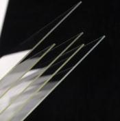
6 Thinner Glass Has Been Increasingly Employed In Evolving Applications of Display Substrates & Cover Glass Gen Size Glass Thickness (mm) Thin m 1 0.5m 1.0m m 6 2.0m 7 2.5m 8 3m 10 Flexible display & electronics e-paper, continuous roll-to-roll component manufacture Mobile LCD panels & touch sensor plates Mobile LCD panels, cover glass, touch sensor plates for notebooks, net-books & mobile internet devices Slates, notebooks, monitors & TVs, small & medium size touch sensors & cover glass Commercial availability Scheduled Development Proposed TV & desktop monitors. Large size cover glass & touch sensor plates 6


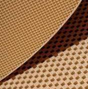
7 Highly Engineered Glass Can Be Both Durable and Clear Superior Mechanical Attributes 7


8 Glass Can Contribute to 3D-IC Technology Enabling Higher Performance Devices Glass as a Carrier Glass an Interposer or PCB IC Glass Interposer IC Glass PCB Glass can be extraordinarily uniform and isotropic Fusion glass can be extraordinarily flat Composition can be tailored for the specific material properties Can be manufactured to final thickness without polishing Flexible in size and format Robust display glass ecosystem can be adapted to semiconductor packaging 8

 Tailorable Thermal Dissipation With Cu TPV")
9 Glass Enables Cost-Effective Solutions For High Volume Manufacturing Ideal Properties Options for High Volume Manufacturing Ultra-High Resistivity, Low Dielectric Constant, Ultra-Low Electrical Loss Tailorable CTE for SMT-to-Board Thin, Ultra-Thin, Ultra-Flat Emerging Approaches To Vias Large Area (Wafer Panel Roll) Tailorable Thermal Dissipation With Cu TPV Source: GaTech 9


10 Possible Path for Higher Production of Interposers Large Area (Wafer Panel Roll) Roll-to Roll Panel Wafer 10


 Average")
11 Continued Progress to Ultra-Flat Thin, Ultra-Thin, Ultra-Flat Champion Wafer Specs (a) Average TTV = 0.8 µm (b) Average Flatness = 17 µm 11


12 Thermal Reliability Ultra-High Resistivity, Low Dielectric Constant, Ultra-Low Electrical Loss Glass flexibility with respect to CTE allows for better management of stack warp. Si Interposer Glass Interposer 3 ppm/ C ~3 ppm/ C 3ppm/ C ~8-10 ppm/ C 15 ppm/ C 15 ppm/ C Silicon 2.5D Interposer Glass 2.5D Interposer 12
 Best Case")

13 Higher Bandwidth Ultra-High Resistivity, Low Dielectric Constant, Ultra-Low Electrical Loss Signal Path Delays in 3D-IC Total Signal Path Delay (ps) Best Case Worse Case 10-30µm 0.1-1µm oxide liner Traditional Silicon Interposer 5-10µm 3D ICs with TSV 0.1-1µm oxide liner 10-30µm NO liner needed GT 3D Glass Interposer Source: GaTech PRC 13
14 Glass Electrical Properties Significantly Reduce Signal Loss Signal Loss Measured at Georgia Tech Ultra-High Resistivity, Low Dielectric Constant, Ultra-Low Electrical Loss 6.2mm CPW in Glass Interposer 1.0mm CPW in Wafer Si Interposer Insertion Loss/mm at 10 GHz: Glass interposer: 0.06 db Wafer-Si interposer: 1.16 db CPW = Coplanar Waveguide 10x lower signal loss in glass for a 6x longer interconnect than silicon (~60x lower leakage improves power efficiency) Source: GaTech PRC 14
 32 Transistors per I/O Driver Glass interposer enables high")
15 Glass Interposer Reduces Power Consumption of High Bandwidth Interconnects Interposer Technology Ultra-High Resistivity, Low Dielectric Constant, Ultra-Low Electrical Loss Glass 128 Larger Driver Size = Higher Power Consumption Wafer Si Transistors per I/O Driver Glass 180 Wafer Si Cannot Transmit Data Signal Delay (ps) 32 Transistors per I/O Driver Glass interposer enables high bandwidth with smaller I/O drivers leading to low power consumption at system level Higher parasitics of Wafer Si signal lines necessitates larger I/O drivers requiring higher power Significant reduction in signal delay in glass also enables higher data rates Source: GaTech PRC 15


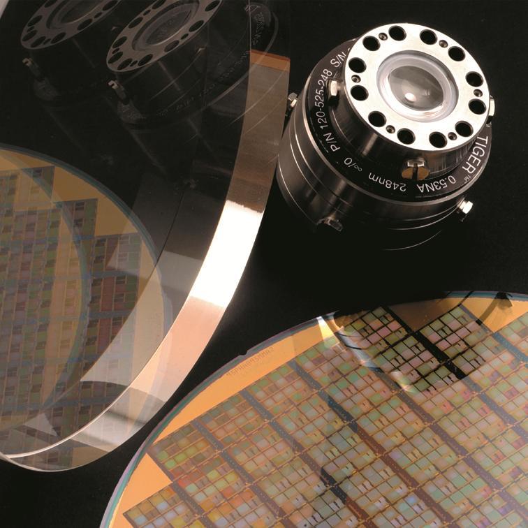
16 Demonstration Vias in High Quality Glass Substrates Emerging Approaches to Vias Ultra-slim glass has significant opportunities to simplify TGV manufacturing processes. Capabilities up to 300mm wafers and panels up to 0.5M 11,716 holes 2,500 holes 30 µm Diameter Blind Holes X-SEM Cu Filling Performance With TGV Substrate Based On Corning Fusion Glass Fully Patterned Wafers With 100,000s of holes Blind Via Diameter ~ 27 µm 16


17 Flexible Glass Applications Roadmap Lab-scale Device Demos Initial Commercial Products Next-Generation Technologies HP Oxide TFTs OLED or LCD Color Filter Flexible display E-Paper WMU / CAMM Organic PV ITRI-DTC Ch-LC display ProCap Touch Sensor OLED lighting Organic PV University of Stuttgart TFT-LCD Flexible CIGS PV panels Roll-to-roll displays Glass with Vias
18 The Final Word For more than 160 years, our scientists and engineers have taken advantage of the technical and aesthetic properties of glass to drive new innovations We re amazed by its strength, stability, versatility, and complex engineering No other material provides such a perfect marriage of form and function. Wendell P. Weeks, Chairman & CEO, Corning Incorporated 18
19 Forward Looking And Cautionary Statements This presentation contains forward looking statements that involve a variety of business risks and other uncertainties that could cause actual results to differ materially. These risks and uncertainties include the possibility of changes or fluctuations in global economic conditions; currency exchange rates; product demand and industry capacity; competitive products and pricing; availability and costs of critical components and materials; new product development and commercialization; order activity and demand from major customers; capital spending by larger customers in the telecommunications industry and other business segments; the mix of sales between premium and non-premium products; possible disruption in commercial activities due to terrorist activity and armed conflict; ability to obtain financing and capital on commercially reasonable terms; acquisition and divestiture activities; the level of excess or obsolete inventory; the ability to enforce patents; product and components performance issues; and litigation. These and other risk factors are identified in Corning s filings with the Securities and Exchange Commission. Forward looking statements speak only as of the day that they are made, and Corning undertakes no obligation to update them in light of new information or future events. 19


20 20
LSI ON GLASS SUBSTRATES
 LSI ON GLASS SUBSTRATES OUTLINE Introduction: Why System on Glass? MOSFET Technology Low-Temperature Poly-Si TFT Technology System-on-Glass Technology Issues Conclusion System on Glass CPU SRAM DRAM EEPROM
Signal Integrity Modeling and Measurement of TSV in 3D IC
 Signal Integrity Modeling and Measurement of TSV in 3D IC Joungho Kim KAIST joungho@ee.kaist.ac.kr 1 Contents 1) Introduction 2) 2.5D/3D Architectures with TSV and Interposer 3) Signal integrity, Channel
Through Glass Via (TGV) Technology for RF Applications
 Technology for RF Applications") Through Glass Via (TGV) Technology for RF Applications C. H. Yun 1, S. Kuramochi 2, and A. B. Shorey 3 1 Qualcomm Technologies, Inc. 5775 Morehouse Dr., San Diego, California 92121, USA Ph: +1-858-651-5449,
Through Glass Via (TGV) Technology for RF Applications C. H. Yun 1, S. Kuramochi 2, and A. B. Shorey 3 1 Qualcomm Technologies, Inc. 5775 Morehouse Dr., San Diego, California 92121, USA Ph: +1-858-651-5449,
450mm and Moore s Law Advanced Packaging Challenges and the Impact of 3D
 450mm and Moore s Law Advanced Packaging Challenges and the Impact of 3D Doug Anberg VP, Technical Marketing Ultratech SOKUDO Lithography Breakfast Forum July 10, 2013 Agenda Next Generation Technology
Substrate-Integrated Waveguides in Glass Interposers with Through-Package-Vias
 Substrate-Integrated Waveguides in Glass Interposers with Through-Package-Vias Jialing Tong, Venky Sundaram, Aric Shorey +, and Rao Tummala 3D Systems Packaging Research Center Georgia Institute of Technology,
Plan Optik AG. Plan Optik AG PRODUCT CATALOGUE
 Plan Optik AG Plan Optik AG PRODUCT CATALOGUE 2 In order to service the high demand of wafers more quickly, Plan Optik provides off the shelf products in sizes from 2 up to 300mm diameter. Therefore Plan
Intel Demonstrates High-k + Metal Gate Transistor Breakthrough on 45 nm Microprocessors
 Intel Demonstrates High-k + Metal Gate Transistor Breakthrough on 45 nm Microprocessors Mark Bohr Intel Senior Fellow Logic Technology Development Kaizad Mistry 45 nm Program Manager Logic Technology Development
A Miniaturized Multi-Channel TR Module Design Based on Silicon Substrate
 Progress In Electromagnetics Research Letters, Vol. 74, 117 123, 2018 A Miniaturized Multi-Channel TR Module Design Based on Silicon Substrate Jun Zhou 1, 2, *, Jiapeng Yang 1, Donglei Zhao 1, and Dongsheng
Electrical Characteristics Analysis and Comparison between Through Silicon Via(TSV) and Through Glass Via(TGV)
 and Through Glass Via(TGV)") Electrical Characteristics Analysis and Comparison between Through Silicon Via(TSV) and Through Glass Via(TGV) Jihye Kim, Insu Hwang, Youngwoo Kim, Heegon Kim and Joungho Kim Department of Electrical Engineering
Electrical Characteristics Analysis and Comparison between Through Silicon Via(TSV) and Through Glass Via(TGV) Jihye Kim, Insu Hwang, Youngwoo Kim, Heegon Kim and Joungho Kim Department of Electrical Engineering
3D IC-Package-Board Co-analysis using 3D EM Simulation for Mobile Applications
 3D IC-Package-Board Co-analysis using 3D EM Simulation for Mobile Applications Darryl Kostka, CST of America Taigon Song and Sung Kyu Lim, Georgia Institute of Technology Outline Introduction TSV Array
Modeling, Design, and Demonstration of 2.5D Glass Interposers for 16-Channel 28 Gbps Signaling Applications
 Modeling, Design, and Demonstration of 2.5D Glass Interposers for 16-Channel 28 Gbps Signaling Applications Brett Sawyer, Bruce C. Chou, Saumya Gandhi, Jack Mateosky, Venky Sundaram, and Rao Tummala 3D
Signal Integrity Design of TSV-Based 3D IC
 Signal Integrity Design of TSV-Based 3D IC October 24, 21 Joungho Kim at KAIST joungho@ee.kaist.ac.kr http://tera.kaist.ac.kr 1 Contents 1) Driving Forces of TSV based 3D IC 2) Signal Integrity Issues
Fabricating 2.5D, 3D, 5.5D Devices
 Fabricating 2.5D, 3D, 5.5D Devices Bob Patti, CTO rpatti@tezzaron.com Tezzar on Semiconduct or 04/15/2013 1 Gen4 Dis-Integrated 3D Memory DRAM layers 42nm node 2 million vertical connections per lay per
Gain Slope issues in Microwave modules?
 Gain Slope issues in Microwave modules? Physical constraints for broadband operation If you are a microwave hardware engineer you most likely have had a few sobering experiences when you test your new
Flexible glass substrates for roll-to-roll manufacturing
 Science & Technology Flexible glass substrates for roll-to-roll manufacturing Corning - S. Garner, G. Merz, J. Tosch, C. Chang, D. Marshall, X. Li, J. Matusick, J. Lin, C. Kuo, S. Lewis, C. Kang ITRI -
Silicon Interposers enable high performance capacitors
 Interposers between ICs and package substrates that contain thin film capacitors have been used previously in order to improve circuit performance. However, with the interconnect inductance due to wire
PERSPECTIVES FOR DISRUPTIVE 200MM/8-INCH GAN POWER DEVICE AND GAN-IC TECHNOLOGY DR. DENIS MARCON SR. BUSINESS DEVELOPMENT MANAGER
 PERSPECTIVES FOR DISRUPTIVE 200MM/8-INCH GAN POWER DEVICE AND GAN-IC TECHNOLOGY DR. DENIS MARCON SR. BUSINESS DEVELOPMENT MANAGER What I will show you today 200mm/8-inch GaN-on-Si e-mode/normally-off technology
3D TSV Micro Cu Column Chip-to-Substrate/Chip Assmbly/Packaging Technology
 3D TSV Micro Cu Column Chip-to-Substrate/Chip Assmbly/Packaging Technology by Seung Wook Yoon, *K. T. Kang, W. K. Choi, * H. T. Lee, Andy C. B. Yong and Pandi C. Marimuthu STATS ChipPAC LTD, 5 Yishun Street
Glass Packaging for RF MEMS
 Glass Packaging for RF MEMS Rajiv Parmar and Jay Zhang Corning Incorporated One Riverfront Plaza Corning, NY 14831 USA Email: parmarr@corning.com Chris Keimel Menlo Microsystems 257 Fuller Road, Suite
DuPont Reflections on Photovoltaics
 DuPont Reflections on Photovoltaics Steven C. Freilich Technology Director E. I. du Pont de Nemours and Co. CTO Electronics and Communication April 23, 2009 The Vision of DuPont 2 To be the world s most
EMERGING SUBSTRATE TECHNOLOGIES FOR PACKAGING
 EMERGING SUBSTRATE TECHNOLOGIES FOR PACKAGING Henry H. Utsunomiya Interconnection Technologies, Inc. Suwa City, Nagano Prefecture, Japan henryutsunomiya@mac.com ABSTRACT This presentation will outline
MemsTech MSM3C-S4045 Integrated Silicon Microphone with Supplementary TEM Analysis
 MemsTech MSM3C-S4045 Integrated Silicon Microphone with Supplementary TEM Analysis MEMS Process Review For comments, questions, or more information about this report, or for any additional technical needs
Advanced Packaging Solutions
 Advanced Packaging Solutions by USHIO INC. USHIO s UX Series Providing Advanced Packaging Solutions Page 2 USHIO s UX Series Models Featured @ SEMICON West 2013 Page 2 Large-Size Interposer Stepper UX7-3Di
Electrical Comparison between TSV in Silicon and TPV in Glass for Interposer and Package Applications
 Electrical Comparison between TSV in Silicon and TPV in Glass for Interposer and Package Applications Jialing Tong, Kadppan Panayappan, Venky Sundaram, and Rao Tummala, Fellow, IEEE 3D Systems Packaging
The 3D Silicon Leader
 The 3D Silicon Leader 3D Silicon IPD for smaller and more reliable Implantable Medical Devices ATW on Advanced Packaging for Wireless Medical Devices Mohamed Mehdi Jatlaoui, Sébastien Leruez, Olivier Gaborieau,
No soft touch only automated systems can boost productivity and quality when lapping/polishing fragile GaAs wafers
 No soft touch only automated systems can boost productivity and quality when lapping/polishing fragile GaAs wafers Author: Mark Kennedy www.logitech.uk.com Overview The processing of GaAs (gallium arsenide)
450mm patterning out of darkness Backend Process Exposure Tool SOKUDO Lithography Breakfast Forum July 10, 2013 Doug Shelton Canon USA Inc.
 450mm patterning out of darkness Backend Process Exposure Tool SOKUDO Lithography Breakfast Forum 2013 July 10, 2013 Doug Shelton Canon USA Inc. Introduction Half Pitch [nm] 2013 2014 2015 2016 2017 2018
Chapter 2. Literature Review
 Chapter 2 Literature Review 2.1 Development of Electronic Packaging Electronic Packaging is to assemble an integrated circuit device with specific function and to connect with other electronic devices.
Lecture: Integration of silicon photonics with electronics. Prepared by Jean-Marc FEDELI CEA-LETI
 Lecture: Integration of silicon photonics with electronics Prepared by Jean-Marc FEDELI CEA-LETI Context The goal is to give optical functionalities to electronics integrated circuit (EIC) The objectives
Toshiba HEK3 0.3 Mp VGA CMOS Image Sensor 0.13 µm Toshiba Process
 Toshiba HEK3 0.3 Mp VGA CMOS Image Sensor 0.13 µm Toshiba Process Through Silicon Via Process Review For comments, questions, or more information about this report, or for any additional technical needs
Application of EOlite Flexible Pulse Technology. Matt Rekow Yun Zhou Nicolas Falletto
 Application of EOlite Flexible Pulse Technology Matt Rekow Yun Zhou Nicolas Falletto 1 Topics Company Background What is a Flexible Pulse Laser? Why Tailored or Flexible Pulse? Application of Flexible
Integrated Photonics using the POET Optical InterposerTM Platform
 Integrated Photonics using the POET Optical InterposerTM Platform Dr. Suresh Venkatesan CIOE Conference Shenzhen, China Sept. 5, 2018 POET Technologies Inc. TSXV: PUBLIC POET PTK.V Technologies Inc. PUBLIC
Inductors In Silicon Based on SU-8 Enhanced Silicon Molding Technique for Portable Electronics
 Biophotonics & Microsystems Lab Inductors In Silicon Based on SU-8 Enhanced Silicon Molding Technique for Portable Electronics Mingliang Wang 1*, Khai D. T. Ngo 2, Huikai Xie 1 1 BML, University of Florida
ELECTRICAL MODELING, DESIGN, AND HIGH-FREQUENCY CHARACTERISATION OF FINE-PITCH THROUGH-PACKAGE-VIAS IN ULTRA-THIN 3D GLASS INTERPOSER PACKAGES
 ELECTRICAL MODELING, DESIGN, AND HIGH-FREQUENCY CHARACTERISATION OF FINE-PITCH THROUGH-PACKAGE-VIAS IN ULTRA-THIN 3D GLASS INTERPOSER PACKAGES A Dissertation Presented to The Academic Faculty by SUKHADHA
High Frequency Single & Multi-chip Modules based on LCP Substrates
 High Frequency Single & Multi-chip Modules based on Substrates Overview Labtech Microwave has produced modules for MMIC s (microwave monolithic integrated circuits) based on (liquid crystal polymer) substrates
Fan-Out Solutions: Today, Tomorrow the Future Ron Huemoeller
 Fan-Out Solutions: Today, Tomorrow the Future Ron Huemoeller Corporate Vice President, WW RnD & Technology Strategy 1 In the Beginning ewlb 2 Fan Out Packaging Emerges Introduction of Fan Out (ewlb) Marketed
Silicon Photonics Technology Platform To Advance The Development Of Optical Interconnects
 Silicon Photonics Technology Platform To Advance The Development Of Optical Interconnects By Mieke Van Bavel, science editor, imec, Belgium; Joris Van Campenhout, imec, Belgium; Wim Bogaerts, imec s associated
Addressing the Design Challenges of RF/ Millimeter Wave Semiconductor Packaging
 MICROELECTRONIC PACKAGES HEADERS & TERMINALS CERAMIC SOLUTIONS Addressing the Design Challenges of RF/ Millimeter Wave Semiconductor Packaging Craig Vieira RF Designer IMAPS New England - May 3, 2016 1
Display Materials and Components Report - Glass Slimming 2013
 Display Materials and Components Report - Glass Slimming 2013 May 2013 Doo.Kim@ihs.com www.displaybank.com 1/130 No material contained in this report may be reproduced in whole or in part without the express
/14/$ IEEE 470
 Analysis of Power Distribution Network in Glass, Silicon Interposer and PCB Youngwoo Kim, Kiyeong Kim Jonghyun Cho, and Joungho Kim Department of Electrical Engineering, KAIST Daejeon, South Korea youngwoo@kaist.ac.kr
California Eastern Laboratories
 California Eastern Laboratories 750MHz Power Doubler and Push-Pull CATV Hybrid Modules Using Gallium Arsenide D. McNamara*, Y. Fukasawa**, Y. Wakabayashi**, Y. Shirakawa**, Y. Kakuta** *California Eastern
Electronic Material Systems
 Electronic Material Systems Barry Russell Operating Vice President 1 Safe Harbor Statement Today s presentations may contain forward-looking statements within the meaning of the Private Securities Litigation
Electromagnetic Bandgap Design for Power Distribution Network Noise Isolation in the Glass Interposer
 2016 IEEE 66th Electronic Components and Technology Conference Electromagnetic Bandgap Design for Power Distribution Network Noise Isolation in the Glass Interposer Youngwoo Kim, Jinwook Song, Subin Kim
High-Frequency Characterization of Through Package Vias Formed by Focused Electrical-Discharge in Thin Glass Interposers
 High-Frequency Characterization of Through Package Vias Formed by Focused Electrical-Discharge in Thin Glass Interposers Jialing Tong *, Yoichiro Sato +, Shintaro Takahashi +, Nobuhiko Imajyo +, Andrew
Manufacture and Performance of a Z-interconnect HDI Circuit Card Abstract Introduction
 Manufacture and Performance of a Z-interconnect HDI Circuit Card Michael Rowlands, Rabindra Das, John Lauffer, Voya Markovich EI (Endicott Interconnect Technologies) 1093 Clark Street, Endicott, NY 13760
Put your best ideas forward.
 Improve the way people view your brand. High-performance optical polymers and films for the electronics market Put your best ideas forward. The world is increasingly connected by technology that uses electronic
Fraunhofer IZM - ASSID
 FRAUNHOFER-INSTITUT FÜR Zuverlässigkeit und Mikrointegration IZM Fraunhofer IZM - ASSID All Silicon System Integration Dresden Heterogeneous 3D Wafer Level System Integration 3D system integration is one
POSSUM TM Die Design as a Low Cost 3D Packaging Alternative
 POSSUM TM Die Design as a Low Cost 3D Packaging Alternative The trend toward 3D system integration in a small form factor has accelerated even more with the introduction of smartphones and tablets. Integration
Design and Simulation of Compact, High Capacitance Ratio RF MEMS Switches using High-K Dielectric Material
 Advance in Electronic and Electric Engineering. ISSN 2231-1297, Volume 3, Number 5 (2013), pp. 579-584 Research India Publications http://www.ripublication.com/aeee.htm Design and Simulation of Compact,
Foundry WLSI Technology for Power Management System Integration
 1 Foundry WLSI Technology for Power Management System Integration Chuei-Tang Wang, Chih-Lin Chen, Jeng-Shien Hsieh, Victor C.Y. Chang, Douglas Yu R&D,TSMC Oct. 2016 2 Motivation Outline PMIC system integration
Pierre Brondeau Vice President, Business Group Executive Electronic Materials Regional Director - Europe Lehman Brothers Conference Call November
 Pierre Brondeau Vice President, Business Group Executive Electronic Materials Regional Director - Europe Lehman Brothers Conference Call November 2006 Forward Looking Statement The presentation today may
FORESIGHT AUTONOMOUS HOLDINGS NASDAQ/TASE: FRSX. Investor Conference. December 2018
 FORESIGHT AUTONOMOUS HOLDINGS NASDAQ/TASE: FRSX Investor Conference December 2018 Forward-Looking Statement This presentation of Foresight Autonomous Holdings Ltd. (the Company ) contains forward-looking
21 st Annual Needham Growth Conference
 21 st Annual Needham Growth Conference Investor Presentation January 15, 2019 Safe Harbor Statement The information contained in and discussed during this presentation may include forward-looking statements
CMP for More Than Moore
 2009 Levitronix Conference on CMP Gerfried Zwicker Fraunhofer Institute for Silicon Technology ISIT Itzehoe, Germany gerfried.zwicker@isit.fraunhofer.de Contents Moore s Law and More Than Moore Comparison:
Ultra-thin, highly flexible RF cables and interconnections
 Ultra-thin, highly flexible RF cables and interconnections Hans Burkard, Hightec MC AG, Lenzburg, Switzerland Urs Brunner, Hightec MC AG, Lenzburg, Switzerland Karl Kurz, Hightec MC AG, Lenzburg, Switzerland
Basic Functional Analysis. Sample Report Richmond Road, Suite 500, Ottawa, ON K2H 5B7 Canada Tel:
 Basic Functional Analysis Sample Report 3685 Richmond Road, Suite 500, Ottawa, ON K2H 5B7 Canada Tel: 613-829-0414 www.chipworks.com Basic Functional Analysis Sample Report Some of the information in this
Advances in CO 2 -Laser Drilling of Glass Substrates
 Available online at www.sciencedirect.com Physics Procedia 39 (2012 ) 548 555 LANE 2012 Advances in CO 2 -Laser Drilling of Glass Substrates Lars Brusberg,a, Marco Queisser b, Clemens Gentsch b, Henning
MEMS in ECE at CMU. Gary K. Fedder
 MEMS in ECE at CMU Gary K. Fedder Department of Electrical and Computer Engineering and The Robotics Institute Carnegie Mellon University Pittsburgh, PA 15213-3890 fedder@ece.cmu.edu http://www.ece.cmu.edu/~mems
Thermal Management in the 3D-SiP World of the Future
 Thermal Management in the 3D-SiP World of the Future Presented by W. R. Bottoms March 181 th, 2013 Smaller, More Powerful Portable Devices Are Driving Up Power Density Power (both power delivery and power
Crystals Oscillators Filters Precision Timing Magnetics Engineered Solutions
 Magnetics Engineered Solutions WWW.ABRACON.COM Introduction Purpose: Objectives: Content: Learning Time: Introduce the ASG series, Fixed Frequency XO & VCXO - Explain the benefits of the ASG series of
Optical Characterization and Defect Inspection for 3D Stacked IC Technology
 Minapad 2014, May 21 22th, Grenoble; France Optical Characterization and Defect Inspection for 3D Stacked IC Technology J.Ph.Piel, G.Fresquet, S.Perrot, Y.Randle, D.Lebellego, S.Petitgrand, G.Ribette FOGALE
OB-FPC: FLEXIBLE PRINTED CIRCUITS FOR THE ALICE TRACKER
 OB-FPC: FLEXIBLE PRINTED CIRCUITS FOR THE ALICE TRACKER Main Requirements. The OB FPC must meet demanding requirements: Material: Low material budget Electrical: impedance of differential lines @ 100W,
New Wave SiP solution for Power
 New Wave SiP solution for Power Vincent Lin Corporate R&D ASE Group APEC March 7 th, 2018 in San Antonio, Texas. 0 Outline Challenges Facing Human Society Energy, Environment and Traffic Autonomous Driving
Through-Glass Vias with Laser Precision LPKF Vitrion 5000
 Through-Glass Vias with Laser Precision LPKF Vitrion 5000 Glass Interposers with High-Speed Laser Processing In the interconnection of highly integrated chips with conventional circuit boards, interposers
shaping global nanofuture ULTRA-PRECISE PRINTING OF NANOMATERIALS
 shaping global nanofuture ULTRA-PRECISE PRINTING OF NANOMATERIALS WHO ARE WE? XTPL S.A. is a company operating in the nanotechnology segment. The interdisciplinary team of XTPL develops on a global scale
AGC Glass Technology Solution to Highly Functional Display Needs
 AGC Glass Technology Solution to Highly Functional Display Needs Takahiro IKEZAKI Vice President Electronics Glass General Division, AGC Electronics, Asahi Glass Co., Ltd. June 5, 2012 -Contents- AGC Strengths
Application Note 5012
 MGA-61563 High Performance GaAs MMIC Amplifier Application Note 5012 Application Information The MGA-61563 is a high performance GaAs MMIC amplifier fabricated with Avago Technologies E-pHEMT process and
End-of-line Standard Substrates For the Characterization of organic
 FRAUNHOFER INSTITUTe FoR Photonic Microsystems IPMS End-of-line Standard Substrates For the Characterization of organic semiconductor Materials Over the last few years, organic electronics have become
Design and Modeling of Through-Silicon Vias for 3D Integration
 Design and Modeling of Through-Silicon Vias for 3D Integration Ivan Ndip, Brian Curran, Gerhard Fotheringham, Jurgen Wolf, Stephan Guttowski, Herbert Reichl Fraunhofer IZM & BeCAP @ TU Berlin IEEE Workshop
Flexible Glass Applications & Process Scaling
 Flexible Glass Applications & Process Scaling Sean Garner, Sue Lewis, Gary Merz, Alex Cuno, Ilia Nikulin October 16, 2017 Outline Flexible Glass Applications Process Scaling Summary 2 Flexible Glass Enables
CMOS Digital Integrated Circuits Lec 2 Fabrication of MOSFETs
 CMOS Digital Integrated Circuits Lec 2 Fabrication of MOSFETs 1 CMOS Digital Integrated Circuits 3 rd Edition Categories of Materials Materials can be categorized into three main groups regarding their
SiP packaging technology of intelligent sensor module. Tony li
 SiP packaging technology of intelligent sensor module Tony li 2016.9 Contents What we can do with sensors Sensor market trend Challenges of sensor packaging SiP technology to overcome challenges Overview
Flip-Chip for MM-Wave and Broadband Packaging
 1 Flip-Chip for MM-Wave and Broadband Packaging Wolfgang Heinrich Ferdinand-Braun-Institut für Höchstfrequenztechnik (FBH) Berlin / Germany with contributions by F. J. Schmückle Motivation Growing markets
Micromachining of Glass by Laser Induced Deep Etching (LIDE) LPKF Vitrion 5000
 LPKF Vitrion 5000") Micromachining of Glass by Laser Induced Deep Etching (LIDE) LPKF Vitrion 5000 In microsystems technology, glass is very suitable as a substrate material for a variety of applications. The basis for the
Micromachining of Glass by Laser Induced Deep Etching (LIDE) LPKF Vitrion 5000 In microsystems technology, glass is very suitable as a substrate material for a variety of applications. The basis for the
Corning s R&D / Innovation Approach
 Corning s R&D / Innovation Approach October 17, 2011 American Institute of Chemical Engineers Joseph A. Miller, Ph.D. Executive Vice President Chief Technology Officer Corporate Snapshot Corning Incorporated
Nikon Medium Term Management Plan
 NIKON CORPORATION Mar.30,2006 Nikon Medium Term Management Plan March 30, 2006 NIKON CORPORATION This presentation contains forward-looking statements with respect to future results, performance and achievements
Semiconductor Back-Grinding
 Semiconductor Back-Grinding The silicon wafer on which the active elements are created is a thin circular disc, typically 150mm or 200mm in diameter. During diffusion and similar processes, the wafer may
CMP for Advanced Packaging
 CMP for Advanced Packaging Robert L. Rhoades, Ph.D. NCCAVS TFUG-CMPUG Joint Meeting June 9, 2016 Semiconductor Equipment Spare Parts and Service CMP Foundry Foundry Click to edit Master Outline title style
IMPACT OF 450MM ON CMP
 IMPACT OF 450MM ON CMP MICHAEL CORBETT MANAGING PARTNER LINX CONSULTING, LLC MCORBETT@LINX-CONSULTING.COM PREPARED FOR CMPUG JULY 2011 LINX CONSULTING Outline 1. Overview of Linx Consulting 2. CMP Outlook/Drivers
Silicon Photonics Transceivers for Hyper Scale Datacenters: Deployment and Roadmap
 Silicon Photonics Transceivers for Hyper Scale Datacenters: Deployment and Roadmap Peter De Dobbelaere Luxtera Inc. 09/19/2016 Luxtera Proprietary www.luxtera.com Luxtera Company Introduction $100B+ Shift
Ultra-Thin, Highly Flexible Cables and Interconnections for Low and High Frequencies
 Ultra-Thin, Highly Flexible Cables and Interconnections for Low and High Frequencies Hans Burkard a, Tobias Lamprecht b, Thomas Morf b, Bert Jan Offrein b, Josef Link a a Hightec MC AG, Fabrikstrasse,
IEEE JOURNAL OF SELECTED TOPICS IN QUANTUM ELECTRONICS 2010 Silicon Photonic Circuits: On-CMOS Integration, Fiber Optical Coupling, and Packaging
 IEEE JOURNAL OF SELECTED TOPICS IN QUANTUM ELECTRONICS 2010 Silicon Photonic Circuits: On-CMOS Integration, Fiber Optical Coupling, and Packaging Christophe Kopp, St ephane Bernab e, Badhise Ben Bakir,
Radio Frequency Electronics
 Radio Frequency Electronics Preliminaries IV Born 22 February 1857, died 1 January 1894 Physicist Proved conclusively EM waves (theorized by Maxwell ), exist. Hz names in his honor. Created the field of
InvenSense IDG-300 Dual-Axis Angular Rate Gyroscope Sensor
 InvenSense IDG-300 Dual-Axis Angular Rate Gyroscope Sensor MEMS Process Review For comments, questions, or more information about this report, or for any additional technical needs concerning semiconductor
Surface Mount Package SOT-363/SC70. Pin Connections and Package Marking. AHx
 Agilent ABA-5153 3.5 GHz Broadband Silicon RFIC Amplifier Data Sheet Description Agilent s ABA-5153 is an economical, easy-to-use, internally 5-ohm matched silicon monolithic broadband amplifier that offers
First Demonstration of Panel Glass Fan-out (GFO) Packages for High I/O Density and High Frequency Multi-Chip Integration
 Packages for High I/O Density and High Frequency Multi-Chip Integration") First Demonstration of Panel Glass Fan-out (GFO) Packages for High I/O Density and High Frequency Multi-Chip Integration Tailong Shi, Chintan Buch,Vanessa Smet, Yoichiro Sato, Lutz Parthier, Frank Wei
First Demonstration of Panel Glass Fan-out (GFO) Packages for High I/O Density and High Frequency Multi-Chip Integration Tailong Shi, Chintan Buch,Vanessa Smet, Yoichiro Sato, Lutz Parthier, Frank Wei
200mm and 300mm Test Patterned Wafers for Bonding Process Applications SKW ASSOCIATES, INC.
 C M P C h a r a c t e r I z a t I o n S o l u t I o n s 200mm and 300mm Test Patterned Wafers for Bonding Process Applications SKW ASSOCIATES, INC. 2920 Scott Blvd., Santa Clara, CA 95054 Tel: 408-919-0094,
How material engineering contributes to delivering innovation in the hyper connected world
 How material engineering contributes to delivering innovation in the hyper connected world Paul BOUDRE, Soitec CEO Leti Innovation Days - July 2018 Grenoble, France We live in a world of data In perpetual
True Three-Dimensional Interconnections
 True Three-Dimensional Interconnections Satoshi Yamamoto, 1 Hiroyuki Wakioka, 1 Osamu Nukaga, 1 Takanao Suzuki, 2 and Tatsuo Suemasu 1 As one of the next-generation through-hole interconnection (THI) technologies,
3. Details on microwave PCB-materials like {ε r } etc. can be found in the Internet with Google for example: microwave laminates comparison.
 1. Introduction 1. As widely known for microwave PCB-design it is essential to obey the electromagnetic laws. RF-impedance matching therefore is a must. For the following steps one of the following tools
Flexible Hybrid Electronics Fabricated with High-Performance COTS ICs using RTI CircuitFilm TM Technology
 Flexible Hybrid Electronics Fabricated with High-Performance COTS ICs using RTI CircuitFilm TM Technology Scott Goodwin 1, Erik Vick 2 and Dorota Temple 2 1 Micross Advanced Interconnect Technology Micross
Chapter 7 Introduction to 3D Integration Technology using TSV
 Chapter 7 Introduction to 3D Integration Technology using TSV Jin-Fu Li Department of Electrical Engineering National Central University Jungli, Taiwan Outline Why 3D Integration An Exemplary TSV Process
Application Note 5011
 MGA-62563 High Performance GaAs MMIC Amplifier Application Note 511 Application Information The MGA-62563 is a high performance GaAs MMIC amplifier fabricated with Avago Technologies E-pHEMT process and
Signal and Power Integrity Analysis in 2.5D Integrated Circuits (ICs) with Glass, Silicon and Organic Interposer
 with Glass, Silicon and Organic Interposer") Signal and Power Integrity Analysis in 2.5D Integrated Circuits (ICs) with Glass, Silicon and Organic Interposer Youngwoo Kim 1, Jonghyun Cho 1, Kiyeong Kim 1, Venky Sundaram 2, Rao Tummala 2 and Joungho
Signal and Power Integrity Analysis in 2.5D Integrated Circuits (ICs) with Glass, Silicon and Organic Interposer Youngwoo Kim 1, Jonghyun Cho 1, Kiyeong Kim 1, Venky Sundaram 2, Rao Tummala 2 and Joungho
3D ICs: Recent Advances in the Industry
 3D ICs: Recent Advances in the Industry Suresh Ramalingam Senior Director, Advanced Packaging Outline 3D IC Background 3D IC Technology Development Summary Acknowledgements Stacked Silicon Interconnect
Lithography. Development of High-Quality Attenuated Phase-Shift Masks
 Lithography S P E C I A L Development of High-Quality Attenuated Phase-Shift Masks by Toshihiro Ii and Masao Otaki, Toppan Printing Co., Ltd. Along with the year-by-year acceleration of semiconductor device
Okamoto Machine Tool Works, LTD. June 22, th SEMATECH Symposium Japan 1
 Okamoto Machine Tool Works, LTD 1 Contents Solutions for TSV Wafer Thinning Process (Front Side Via) TSV Wafer Thinning Challenges Process Improvement (4-years Development) TSV Wafer Thinning Tool (TSV300)
Innovations Push Package-on-Package Into New Markets. Flynn Carson. STATS ChipPAC Inc Kato Rd Fremont, CA 94538
 Innovations Push Package-on-Package Into New Markets by Flynn Carson STATS ChipPAC Inc. 47400 Kato Rd Fremont, CA 94538 Copyright 2010. Reprinted from Semiconductor International, April 2010. By choosing
DUV. Matthew McLaren Vice President Program Management, DUV. 24 November 2014
 DUV Matthew McLaren Vice President Program Management, DUV 24 Forward looking statements This document contains statements relating to certain projections and business trends that are forward-looking,
The Future of Packaging ~ Advanced System Integration
 The Future of Packaging ~ Advanced System Integration Enabling a Microelectronic World R. Huemoeller SVP, Adv. Product / Platform Develop June 2013 Product Segments End Market % Share Summary 2 New Product